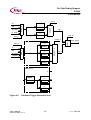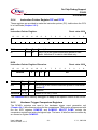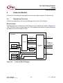
1
Us er’s Ma nual, V 1 .1 , A ugust 2001
C166S
On Chip Debug Support
M i c r o c o n t ro l le r s
N e v e r
s t o p
t h i n k i n g .
Edition 2001-08
Published by Infineon Technologies AG,
St.-Martin-Strasse 53,
D-81541 München, Germany
© Infineon Technologies AG 2001.
All Rights Reserved.
Attention please!
The information herein is given to describe certain components and shall not be considered as warranted
characteristics.
Terms of delivery and rights to technical change reserved.
We hereby disclaim any and all warranties, including but not limited to warranties of non-infringement, regarding
circuits, descriptions and charts stated herein.
Infineon Technologies is an approved CECC manufacturer.
Information
For further information on technology, delivery terms and conditions and prices please contact your nearest
Infineon Technologies Office in Germany or our Infineon Technologies Representatives worldwide (see address
list).
Warnings
Due to technical requirements components may contain dangerous substances. For information on the types in
question please contact your nearest Infineon Technologies Office.
Infineon Technologies Components may only be used in life-support devices or systems with the express written
approval of Infineon Technologies, if a failure of such components can reasonably be expected to cause the failure
of that life-support device or system, or to affect the safety or effectiveness of that device or system. Life support
devices or systems are intended to be implanted in the human body, or to support and/or maintain and sustain
and/or protect human life. If they fail, it is reasonable to assume that the health of the user or other persons may
be endangered.
Us er’ s Ma nual, V 1 .1 , A ugust 2001
C166S
On Chip Debug Support
M i c r o c o n t ro l le r s
N e v e r
s t o p
t h i n k i n g .
C166S
Revision History:
2001-08
Previous Version:
V 1.0
Page
Subjects (major changes since last revision)
23
Common Considerations on Accessing OCDS Registers
24
General Workaround to Avoid Software Problems with OCDS
V 1.1
Language corrections
We Listen to Your Comments
Any information within this document that you feel is wrong, unclear or missing at all?
Your feedback will help us to continuously improve the quality of this document.
Please send your proposal (including a reference to this document) to:
[email protected]
On Chip Debug Support
C166S
1
Overview, Features and Applications . . . . . . . . . . . . . . . . . . . . . . . . . . . 3
2
2.1
2.2
2.3
2.4
2.4.1
2.4.2
2.4.3
2.4.4
2.5
2.5.1
2.5.2
2.5.3
2.5.4
2.5.5
2.6
2.6.1
2.6.2
2.6.3
2.6.4
2.6.5
2.6.6
2.6.7
2.7
OCDS Module . . . . . . . . . . . . . . . . . . . . . . . . . . . . . . . . . . . . . . . . . . . . . . . 5
Introduction . . . . . . . . . . . . . . . . . . . . . . . . . . . . . . . . . . . . . . . . . . . . . . . . . 5
Enabling and Disabling the OCDS . . . . . . . . . . . . . . . . . . . . . . . . . . . . . . . . 7
Reset to Halt Mode . . . . . . . . . . . . . . . . . . . . . . . . . . . . . . . . . . . . . . . . . . . 8
Debug Event Sources . . . . . . . . . . . . . . . . . . . . . . . . . . . . . . . . . . . . . . . . . 9
Hardware Trigger Combinations . . . . . . . . . . . . . . . . . . . . . . . . . . . . . . . 9
Execution of a DEBUG Instruction . . . . . . . . . . . . . . . . . . . . . . . . . . . . . 11
Break Pin Input . . . . . . . . . . . . . . . . . . . . . . . . . . . . . . . . . . . . . . . . . . . 11
Event Prioritizing . . . . . . . . . . . . . . . . . . . . . . . . . . . . . . . . . . . . . . . . . . 11
Debug Event Actions . . . . . . . . . . . . . . . . . . . . . . . . . . . . . . . . . . . . . . . . . 12
Trigger Data Transfer (DPEC) . . . . . . . . . . . . . . . . . . . . . . . . . . . . . . . . 12
Call a Monitor . . . . . . . . . . . . . . . . . . . . . . . . . . . . . . . . . . . . . . . . . . . . . 12
Halt Mode . . . . . . . . . . . . . . . . . . . . . . . . . . . . . . . . . . . . . . . . . . . . . . . 13
Activate External Pin . . . . . . . . . . . . . . . . . . . . . . . . . . . . . . . . . . . . . . . 14
Single Stepping . . . . . . . . . . . . . . . . . . . . . . . . . . . . . . . . . . . . . . . . . . . 14
Registers . . . . . . . . . . . . . . . . . . . . . . . . . . . . . . . . . . . . . . . . . . . . . . . . . . 15
Debug Event Control Registers (DEXEVT, DSWEVT, DTREVT) . . . . . 16
Debug Status Register DBGSR . . . . . . . . . . . . . . . . . . . . . . . . . . . . . . . 19
Task ID Register DTIDR . . . . . . . . . . . . . . . . . . . . . . . . . . . . . . . . . . . . 20
Instruction Pointer Register DIP and DIPX . . . . . . . . . . . . . . . . . . . . . . 21
Hardware Trigger Comparison Registers . . . . . . . . . . . . . . . . . . . . . . . 21
Common Considerations on Accessing OCDS Registers . . . . . . . . . . . 23
General Workaround to Avoid Software Problems with OCDS . . . . . . . 24
Reset Behavior . . . . . . . . . . . . . . . . . . . . . . . . . . . . . . . . . . . . . . . . . . . . . 25
3
3.1
3.2
3.3
3.3.1
3.3.2
3.3.3
3.3.4
3.4
JTAG Module . . . . . . . . . . . . . . . . . . . . . . . . . . . . . . . . . . . . . . . . . . . . . .
JTAG Controller State Machine . . . . . . . . . . . . . . . . . . . . . . . . . . . . . . . . .
JTAG Instructions . . . . . . . . . . . . . . . . . . . . . . . . . . . . . . . . . . . . . . . . . . .
Registers . . . . . . . . . . . . . . . . . . . . . . . . . . . . . . . . . . . . . . . . . . . . . . . . . .
BYPASS Register . . . . . . . . . . . . . . . . . . . . . . . . . . . . . . . . . . . . . . . . .
ID Register . . . . . . . . . . . . . . . . . . . . . . . . . . . . . . . . . . . . . . . . . . . . . . .
IOPATH Register . . . . . . . . . . . . . . . . . . . . . . . . . . . . . . . . . . . . . . . . . .
CCONF Register . . . . . . . . . . . . . . . . . . . . . . . . . . . . . . . . . . . . . . . . . .
Steps to Initialize the JTAG Module . . . . . . . . . . . . . . . . . . . . . . . . . . . . . .
27
29
30
31
31
31
32
33
34
4
4.1
4.1.1
4.1.2
4.1.3
4.1.4
4.1.5
Cerberus Module . . . . . . . . . . . . . . . . . . . . . . . . . . . . . . . . . . . . . . . . . . .
Operational Overview . . . . . . . . . . . . . . . . . . . . . . . . . . . . . . . . . . . . . . . .
Definitions . . . . . . . . . . . . . . . . . . . . . . . . . . . . . . . . . . . . . . . . . . . . . . .
Serial Bit Stream Syntax (TDI, TDO) . . . . . . . . . . . . . . . . . . . . . . . . . . .
I/O Instructions . . . . . . . . . . . . . . . . . . . . . . . . . . . . . . . . . . . . . . . . . . . .
Shift Register Behavior . . . . . . . . . . . . . . . . . . . . . . . . . . . . . . . . . . . . .
Data Transfer Examples . . . . . . . . . . . . . . . . . . . . . . . . . . . . . . . . . . . .
35
35
36
36
37
39
39
User’s Manual
OCDS C166S, V 1.0
I-1
V 1.1, 2001-08
On Chip Debug Support
C166S
4.2
4.2.1
4.2.2
4.2.3
4.2.4
4.2.5
4.2.6
4.2.7
4.3
4.3.1
4.3.2
4.3.3
4.3.4
4.3.5
4.4
4.5
4.6
4.7
Registers . . . . . . . . . . . . . . . . . . . . . . . . . . . . . . . . . . . . . . . . . . . . . . . . . .
CLIENT_ID Register . . . . . . . . . . . . . . . . . . . . . . . . . . . . . . . . . . . . . . .
IOADDR Register . . . . . . . . . . . . . . . . . . . . . . . . . . . . . . . . . . . . . . . . .
IOCONF Register . . . . . . . . . . . . . . . . . . . . . . . . . . . . . . . . . . . . . . . . .
IOINFO Register . . . . . . . . . . . . . . . . . . . . . . . . . . . . . . . . . . . . . . . . . .
TRADDR Register . . . . . . . . . . . . . . . . . . . . . . . . . . . . . . . . . . . . . . . . .
COMDATA and RWDATA Registers . . . . . . . . . . . . . . . . . . . . . . . . . . .
IOSR Register . . . . . . . . . . . . . . . . . . . . . . . . . . . . . . . . . . . . . . . . . . . .
Operation Modes . . . . . . . . . . . . . . . . . . . . . . . . . . . . . . . . . . . . . . . . . . . .
RW Mode . . . . . . . . . . . . . . . . . . . . . . . . . . . . . . . . . . . . . . . . . . . . . . . .
Communication Mode . . . . . . . . . . . . . . . . . . . . . . . . . . . . . . . . . . . . . .
Triggered Transfers (DPEC) . . . . . . . . . . . . . . . . . . . . . . . . . . . . . . . . .
Tracing with External Bus Address . . . . . . . . . . . . . . . . . . . . . . . . . . . .
Monitor Controlled Tracing . . . . . . . . . . . . . . . . . . . . . . . . . . . . . . . . . .
Error Handling . . . . . . . . . . . . . . . . . . . . . . . . . . . . . . . . . . . . . . . . . . . . . .
System Security . . . . . . . . . . . . . . . . . . . . . . . . . . . . . . . . . . . . . . . . . . . . .
Power Saving . . . . . . . . . . . . . . . . . . . . . . . . . . . . . . . . . . . . . . . . . . . . . . .
Reset Behavior . . . . . . . . . . . . . . . . . . . . . . . . . . . . . . . . . . . . . . . . . . . . .
5
JTAG API . . . . . . . . . . . . . . . . . . . . . . . . . . . . . . . . . . . . . . . . . . . . . . . . . 57
User’s Manual
OCDS C166S, V 1.0
I-2
42
42
43
43
44
44
44
45
47
47
47
49
50
51
53
54
55
56
V 1.1, 2001-08
On Chip Debug Support
C166S
Overview, Features and Applications
1
Overview, Features and Applications
On Chip Debug Support (OCDS) provides key hardware emulation features to a broad
range of customers at minimal cost. It allows breakpoints to be set and memory locations
to be observed during run time.
break_in
OCDS Module
break_out
Emulator,
Debugger
C166S CPU Core
Cerberus Debug Port
Figure 1-1
JTAG
Module
JTAG
(5 Signals)
OCDS System Overview
The overall OCDS system consists of three blocks:
• Break generation unit (OCDS Module)
• Cerberus debug port
• JTAG Module.
Application programmers and system integrators obtain the benefits of OCDS through
the debugger and emulation tools of Infineon’s tool partners.
Note: To ensure the correct function of the debugger tools, direct usage of the OCDS
features of the C166S CPU by the application programmer is not intended: Their
use is reserved for professional debugger and emulation tools.
OCDS Module Features
•
•
•
•
•
•
•
Hardware, software and external pin breakpoints
Up to four instruction pointer breakpoints
Masked comparisons for hardware breakpoints
The OCDS can also be configured by a monitor
Single stepping with monitor or CPU halt
PC is visible in Halt Mode
Compliant to Nexus Class 1 and higher
User’s Manual
OCDS C166S, V 1.0
-3-
V 1.1, 2001-08
On Chip Debug Support
C166S
Overview, Features and Applications
OCDS Module Applications
The purpose of OCDS is to debug the user software running on the CPU in the
customer’s system. This is done with an external debugger that controls the OCDS via
the independent debug port.
Cerberus Features
•
•
•
•
•
•
•
•
•
•
•
•
•
Generic serial link to access the whole 24 bit user address space
Efficient, high performance protocol
External host controls all transactions
JTAG Interface is used as control and data channel
Generic memory read/write functionality (RW Mode)
Full support for communication between monitor and external debugger
Optional error protection
Security mechanism to allow authorized access only
Low end tracing through reads (writes) triggered by the OCDS
Fast tracing through transfer to external bus
Analysis register for internal bus locking situations
Several Cerberusses can be operated across a single JTAG Interface
An API is provided to allow easy multi-core debugging
Cerberus Applications
• Control and data transfer mechanism for OCDS
• Data transfer channel for programming on- and off-chip (non volatile) memory
• Very robust access port for on- and off-chip (across external bus controller) system
analysis and configuration
• Data channel that is independent from user resources; independent for applications
such as manufacturing line flash memory programming or for system calibration
purposes
The target application of the Cerberus is use of the JTAG Interface as an independent
port for OCDS. The external debug hardware can access the OCDS registers and
arbitrary memory locations.
The system architecture is also very well suited for multi-core debugging across a single
JTAG Interface. Up to four Cerberusses can be connected to the JTAG Module and
operated from standard debuggers in one debug session. The JTAG API provides a
straightforward and proven interface for standard debuggers and arbitrates the access
of the JTAG Interface in a transparent way.
User’s Manual
OCDS C166S, V 1.0
-4-
V 1.1, 2001-08
On Chip Debug Support
C166S
OCDS Module
2
OCDS Module
2.1
Introduction
Basic Concept
The debug concept addresses both the generation of debug events and the definition of
event actions taken when a debug event is generated.
Debug Events
Hardware
triggers
Programmable
trigger
combination
Event Actions
Halt
Debug event
processing
Execution of a
DEBUG instruction
Monitor
DPEC
Activate pin
Break pin input
Figure 2-1
OCDS Module Block Diagram
Debug events
• Hardware trigger combination
• Execution of a DEBUG instruction
• Break pin input
Debug event actions
•
•
•
•
Halt the CPU
Call a monitor
Trigger a data transfer (DPEC) executed by Cerberus
Activate external pin
User’s Manual
OCDS C166S, V 1.0
-5-
V 1.1, 2001-08
On Chip Debug Support
C166S
OCDS Module
Register Overview
Table 2-1
OCDS Register Overview
Register
Description
DBGSR
Debug status register
DEXEVT
Specifies action if external break pin asserted
DSWEVT
Specifies action if a DEBUG instruction is executed
DTREVT
Combination criteria for hardware triggers and resulting action
DCMPDP
Data programming register for the compare registers DCMPx
DCMPSP
Select and programming register for the compare registers DCMPx
1)
DCMP0
Hardware event equal comparison register 0
DCMP11)
Hardware event equal comparison register 1
DCMP21)
Hardware event equal comparison register 2
DCMPG1)
Hardware event range comparison register (greater)
DCMPL1)
Hardware event range comparison register (less)
DIP
Instruction pointer register
DIPX
Instruction pointer register extension
DTIDR
Task ID register
1)
Accessed with DCMPSP and DCMPDP.
User’s Manual
OCDS C166S, V 1.0
-6-
V 1.1, 2001-08
On Chip Debug Support
C166S
OCDS Module
2.2
Enabling and Disabling the OCDS
By default, the OCDS is disabled in order to protect the system during normal execution.
Events can be generated only when the OCDS is enabled. The OCDS Module has an
enable signal that is normally connected to the chip internal JTAG reset. This means that
the OCDS is enabled when the JTAG Module is not in reset state. This is always the case
when the external debugger uses Cerberus.
Note: Depending on the system architecture, the enable signal may be controlled by
another source.
The OCDS Module can also be optionally enabled by software. To avoid an unintentional
enabling by an incorrect user program, the following conditions must be true:
1. OCDS is disabled.
2. DTREVT.MUX_E = 10B.
3. DTREVT.SELECT_E!= 00B (enables the equal comparators).
4. DCMP0 comparison matches (independent of SELECT_E).
5. Currently written DBGSR.DEBUG_ENABLED = 1B.
Thus, a monitor must do the following:
1. Write F0FCH to DCMP0 (address of DBGSR).
2. Write 2200H to DTREVT.
3. Write 0001H to DBGSR.
If the OCDS was enabled by software, it can be disabled by a reset only.
Note: This feature (OCDS enabling by software) might be disabled depending on the
system architecture.
User’s Manual
OCDS C166S, V 1.0
-7-
V 1.1, 2001-08
On Chip Debug Support
C166S
OCDS Module
2.3
Reset to Halt Mode
The CPU can be forced directly to Halt Mode (Chapter 2.5.3) after reset. This is
controlled by the CCONF.RST_HLT bit in the JTAG Module. The reset to Halt Mode
requires three steps:
1. Set CCONF.RST_HLT before the CPU reset goes inactive.
2. Set DBGSR.DEBUG_STATE to Halt Mode after the reset is released.
3. Clear CCONF.RST_HLT.
To remove the CPU from Halt Mode, DBGSR.DEBUG_STATE must be set to User
Mode.
Note: This feature (Reset to Halt Mode) might be disabled or controlled by another
mechanism depending on the system architecture, since the JTAG Module is not
a part of the CPU macro and can be modified.
User’s Manual
OCDS C166S, V 1.0
-8-
V 1.1, 2001-08
On Chip Debug Support
C166S
OCDS Module
2.4
Debug Event Sources
2.4.1
Hardware Trigger Combinations
Table 2-2 lists the possible hardware trigger sources:
Table 2-2
Hardware Triggers
Trigger source
Size
Description
TASKID
16 bits
TASKID in DTIDR register.
IP
24 bits
Instruction Pointer.
R_ADR
24 bits
Data address of reads.
W_ADR
24 bits
Data address of writes.
DA
16 bits
Data value (reads or writes)
TASKID is the contents of the DTIDR register. It is used by advanced real time operating
systems to store the Task ID of the active task.
The trigger sources are compared and combined in the hardware trigger generation unit
(Figure 2-2). The hardware trigger generation unit is programmable with the DTREVT
debug event control register. It consists of two paths. The upper path is for one range
comparisons and the lower path for three equal comparisons. The equal path can be
optionally configured for two masked equal comparisons. The configuration options are
described in detail in Chapter 2.6.1.
User’s Manual
OCDS C166S, V 1.0
-9-
V 1.1, 2001-08
On Chip Debug Support
C166S
OCDS Module
com_r
IP
>
trg_r
com_re
DCMPL
mux_r
select_e
mask_e = 0
mux_e
=
DCMP0
W_ADR
TASKID
SELECT_E
DA
MUX_E
IP
=
DCMP1
COM_RE
R_ADR
DCMPG
COM_R
W_ADR
MUX_R
<
DA
ocds_trgevt
trg_e
=
DCMP2
mask_e = 1
0
MASK
=
DCMP0
DCMP1
=
DCMP2
Figure 2-2
Hardware Trigger Generation Unit
User’s Manual
OCDS C166S, V 1.0
-10-
V 1.1, 2001-08
On Chip Debug Support
C166S
OCDS Module
2.4.2
Execution of a DEBUG Instruction
There is a mechanism through which software can explicitly generate a debug event.
This can be used, for instance, by a debugger to patch code held in RAM in order to
implement breakpoints. A special DEBUG (opcode D140H) instruction is defined that is
a User Mode instruction and its operation is dependent on whether OCDS is enabled.
If OCDS is enabled, the DEBUG instruction causes a debug event to be raised and the
action specified in the DSWEVT debug control register is taken. If OCDS is not enabled,
the DEBUG instruction is treated as a NOP.
2.4.3
Break Pin Input
An external debug break pin is provided to allow the debugger to asynchronously
interrupt the processor. The action taken when this signal is asserted is specified in the
DEXEVT debug control registers. This input is sensitive on a negative clock edge
followed by at least two CPU clock cycles where it is 0.
2.4.4
Event Prioritizing
It is possible that more than one event may be raised in a single cycle. In this case, the
priority of events to be handled is based on the sequence in which the events appear in
the event sources list; those listed first are handled before those listed later.
Table 2-3
Debug Event Priority
Event
Debug Event Control Register
Priority
Break pin input
DEXEVT
1 (highest)
Execution of a DEBUG instruction
DSWEVT
2
Hardware trigger combination
DTREVT
3
User’s Manual
OCDS C166S, V 1.0
-11-
V 1.1, 2001-08
On Chip Debug Support
C166S
OCDS Module
2.5
Debug Event Actions
When the OCDS is enabled and a debug event is generated, one of the actions listed in
Table 2-4 is taken. These actions are explained in detail in the following sections.
Table 2-4
Debug Event Actions
Debug Event Action
User Resources
Interruptible? Break before
make?
Activate external pin
-
-
Trigger data transfer (DPEC) Cycle stealing for DPEC Call a monitor
Stack
User address space
(Interrupt address)
Yes
(after entry).
Halt
-
No
2.5.1
Only for
program
address
triggers.
Trigger Data Transfer (DPEC)
Triggering Cerberus to execute a pending transfer (Chapter 4.3.3) is one of the actions
that can be specified to occur when a debug event is raised. This can be used in critical
routines where the system cannot be interrupted to transfer a memory location to the
RWDATA register and read it (trace) through the Cerberus debug port.
2.5.2
Call a Monitor
Calling a monitor with a special debug hardware trap (trap number 8, vector location 20H)
is one of the possible actions to be taken when a debug event is raised. This trap has
the highest priority, but the monitor routine can reduce its own priority level by resetting
the debug flag bit DEBTRAP in the trap flag register TFR and writing the priority to the
ILVL field in the PSW register.
This short entry to an interruptible monitor allows a flexible debug environment to be
defined that is capable of satisfying many of the requirements for efficient debugging of
a real time system. For example, safety critical code can be served while the debugger
is active. The monitor is ended with a regular RETI instruction. The debug flag bit
DEBTRAP has to be cleared on exiting the TRAP routine, otherwise it will be called
again.
User’s Manual
OCDS C166S, V 1.0
-12-
V 1.1, 2001-08
On Chip Debug Support
C166S
OCDS Module
Debug
Highest
Priority
Interrupt A
Debug
Interrupt A
Interrupt B
Interrupt B
Lowest
Priority
Monitor has highest
priority in the system so debug
process cannot be interrupted
Figure 2-3
Interrupt A has higher priority
than monitor and hence will
be served
Simple and Advanced Debug Model
Structure of a non-interruptible Monitor Routine:
1. Do processing (non interruptible).
2. Set DBGSR = 0000H.
3. Clear the DEBTRAP bit in TFR.
4. Return to user program with RETI instruction.
Structure of an interruptible Monitor Routine:
1. Set DBGSR.DEBUG_STATE == 00B (User Mode).
2. Clear the DEBTRAP bit in TFR.
3. Reduce the interrupt level ILVL in W.
4. Do Processing.
5. Set DBGSR = 0000H.
6. Return to user program with RETI instruction.
Note: The reduction of the interrupt priority of the monitor can cause stack overflows. If
the task that causes the debug event has a higher priority than the monitor, the
monitor will be pushed onto the stack again and again.
Note: Care must be taken that the monitor does not cause an event itself. Otherwise it,
will be started again and again and cause stack overflows.
2.5.3
Halt Mode
The system suspends execution by halting the instruction flow and will not respond to
any interrupts. It then relies on the external debug system to interrogate the target
entirely by reading and updating through the Cerberus debug port. The CPU resumes
User’s Manual
OCDS C166S, V 1.0
-13-
V 1.1, 2001-08
On Chip Debug Support
C166S
OCDS Module
in User Mode when the external debug hardware resets the DEBUG_STATE in DBGSR
to User Mode. It also should reset the OCDS_P_SUSPEND and EVENT_SOURCE bits
in DBGSR.
2.5.4
Activate External Pin
An external pin assertion can be specified as a debug event action. This is to be used in
critical routines where the system cannot be interrupted to signal to the external world
that a particular event has happened. This feature could also be useful to synchronize
the internal and external debug hardware or to do profiling. In most cases the break out
pin is active 0 for as long as the trigger condition is met.
2.5.5
Single Stepping
Single stepping can be done in Halt Mode or with a debug monitor.
Single Stepping in Halt Mode
For this behavior, the trigger condition is set to be always true (example: trigger on IP
range with DCMPL = 000000H, DCMPG = 000001H, COM_R = 11B and COM_RE = 0B)
and the BREAK_AFTER_MAKE bit is set in DTREVT. After every restart, the CPU will
be halted again when the next instruction has been executed.
Single Stepping with a Debug Monitor
The advantage of this type of single stepping is that the system can serve high priority
interrupt requests (Chapter 2.5.2). The basic approach is similar to the single stepping
in Halt Mode with two differences:
• The event action is set to Call a monitor
• The code of the interrupt service routines and of the debug monitor may not be part of
the IP address trigger range.
It is recommended to adjust the IP address trigger range to the current (C-) function of
the user code. This results in a step-over behavior if sub-functions are called within this
function. If a step-in behavior is required, an additional single IP address trigger can be
set to the entry of the sub-function and when it is entered, the IP address trigger range
is changed to cover the sub-function.
User’s Manual
OCDS C166S, V 1.0
-14-
V 1.1, 2001-08
On Chip Debug Support
C166S
OCDS Module
2.6
Registers
Table 2-5
OCDS Register Summary
Name
ESFR
Type Description
DBGSR
F0FCH
h
Debug status register
DIPX
F0FAH
h
Instruction pointer register extension
DIP
F0F8H
h
Instruction pointer register
DSWEVT
F0F4H
Specifies action if DEBUG instruction is executed
DEXEVT
F0F2H
Specifies action if external break pin is asserted
DTREVT
F0F0H
Specifies hardware triggers and action
DCMPDP
F0EEH
Data programming register for DCMPx
DCMPSP
F0ECH
Select and programming register for DCMPx
DTIDR
F0D8H
a
Task ID register
-
1)
Hardware event equal comparison register 0
DCMP1
-
1)
Hardware event equal comparison register 1
DCMP2
-1)
Hardware event equal comparison register 2
DCMPG
-1)
Hardware event range comparison register (greater)
DCMPL
-1)
Hardware event range comparison register (less)
DCMP0
1)
Accessed with DCMPSP and DCMPDP.
The register ESFR addresses of OCDS are not product specific. This is possible
because there will be always only one OCDS in the address space. The fixed addresses
also eliminate the need for the external debugger to have product specific information to
operate the OCDS.
User’s Manual
OCDS C166S, V 1.0
-15-
V 1.1, 2001-08
On Chip Debug Support
C166S
OCDS Module
2.6.1
Debug Event Control Registers (DEXEVT, DSWEVT, DTREVT)
Each possible source of a debug event has an associated register that defines which
action should be taken when that debug event is raised. The debug event control
registers have the same structure for all currently defined sources.
DEXEVT
DSWEVT
Break Pin and Software Debug Event Control Registers
Reset value 0000H
15
14
13
12
11
10
9
8
7
6
5
4
0
0
0
0
0
0
0
0
0
0
ACT.
PIN
0
rw
3
2
1
PER. EVENT_ACTION
STP.
rw
rw
Field
Bits
Type Description
EVENT_ACTION
[2:0]
rw
Defines action taken on debug event:
000 None
001 Software Debug Mode
010 Halt Debug Mode
011 Reserved
100 Reserved
101 Execute DPEC
110 Reserved
111 Set event source bit in DBGSR only
rw
0
PERIPHERALS_STOP [3]
0
Peripherals are not affected by this
event
Sensitive peripherals suspend
operation if event occurs.
1
-
[4]
0
Reserved
ACTIVATE_PIN
[5]
rw
0
1
-
[15:6] 0
External pin always inactive
External pin is active during debug
event
Reserved
EVENT_ACTION specifies what happens when the associated debug event is raised.
The event specifier can have one of the indicated values. For Software and Halt Mode,
the lower two bits of the EVENT_ACTION set the DEBUG_STATE field in DBGSR.
The PERIPHERALS_STOP bit controls the operation mode of the peripherals when the
associated debug event is raised. If this bit is set, the OCDS_P_SUSPEND bit in
DBGSR will be set; this causes sensitive peripherals to suspend.
User’s Manual
OCDS C166S, V 1.0
-16-
V 1.1, 2001-08
On Chip Debug Support
C166S
OCDS Module
Note: Presently, OCDS_P_SUSPEND is set only when the associated
EVENT_ACTION is either Halt Mode or Software Debug Mode. This may change
in future versions of OCDS.
DTREVT
Hardware Trigger Combination Debug Event Control
15
14
13
12
11
COM SELECT
RE
E
M.
E.
COM_R
MUX_E
MUX_R
rw
rw
rw
rw
rw
rw
10
9
8
7
6
Reset value 0000H
5
4
3
2
1
0
ACT. B.
A. PER.
PIN M.
STP. EVENT_ACTION
rw
rw
rw
rw
Field
Bits
Type Description
EVENT_ACTION
[2:0]
rw
Identical to EVENT_ACTION in DEXEVT
PERIPHERALS_STOP
[3]
rw
Identical to PERIPHERALS_STOP in
DEXEVT
BREAK_AFTER_MAKE [4]
rw
0
1
ACTIVATE_PIN
[5]
rw
Identical to ACTIVATE_PIN in DEXEVT
MUX_R
[7:6]
rw
Range comparison input mux (Figure 2-2):
00
Instruction pointer (IP)
01
Data value (DA)
10
Write address (W_ADR)
11
Read address (R_ADR)
MUX_E
[9:8]
rw
Equal comp. input mux (Figure 2-2) control:
00
Instruction pointer (IP)
01
Data value (DA)
10
Write address (W_ADR)
11
Task ID (TASKID)
COM_R
[11:10] rw
Select range comparison (Table 2-6)
MASK_E
[12]
0
rw
1
Break before make (IP only)
Break after make (IP only)
Unmasked equal comparison
(Figure 2-2)
Masked equal comparison
SELECT_E
[14:13] rw
Select equal comparison (Table 2-7)
COM_RE
[15]
Equal and range comparison combination
01) ocds_trgevt signal is trg_r OR trg_e
1
ocds_trgevt signal is trg_r AND trg_e
User’s Manual
OCDS C166S, V 1.0
rw
-17-
V 1.1, 2001-08
On Chip Debug Support
C166S
OCDS Module
1)
The first option (OR) is intended to be used for the case mux_r == mux_e only and in particular to have four
IP triggers. In case of different comparison sources this option results in a complex behavior, because the
triggers of for instance IP and W_ADR are created in different pipeline stages of the CPU.
The COM_R field enables the range comparison to be included in the ocds_trgevt
generation (Figure 2-2). For in-range comparisons, DCMPG is used as the upper
boundary and DCMPL is the lower boundary. For out-of-range comparisons, it is the
other way round. Table 2-6 lists the options:.
Table 2-6
COM_R Field of DTREVT
Value trg_r signal
00
0 (not enabled)
01
In range: 1 if DCMPG > input > DCMPL, otherwise 0
10
Reserved
11
Out of range: 1 if (DCMPG > input) or (input > DCMPL), otherwise 0
The MASK_E bit distinguishes between masked or unmasked input for the equal
comparison (Figure 2-2). In the masked case, DCMP0 controls the relevant bits for the
comparison. All bits of the input signal where the associated DCMP0 bit is 0 are also set
to 0 prior to the comparison. Note that the comparison values in DCMP1 and DCMP2
must also be 0 where the DCMP0 mask is 0. Otherwise, the comparison will not match.
The SELECT_E field enables the equal comparisons to be included in the ocds_trgevt
generation and selects which is used (Figure 2-2). Note that for masked comparisons,
the SELECT_E field must be set to 10B or 11B. Table 2-7 lists the options:.
Table 2-7
SELECT_E Field
Value mask_e trg_e signal
00
0
0 (not enabled)
01
1 if DCMP0 matches, otherwise 0
10
1 if DCMP0 or DCMP1 match, otherwise 0
11
1 if DCMP0 or DCMP1 or DCMP2 match, otherwise 0
00
1
0 (not enabled)
01
0 (always)
10
1 if DCMP1 matches, otherwise 0
11
1 if DCMP1 or DCMP2 match, otherwise 0
User’s Manual
OCDS C166S, V 1.0
-18-
V 1.1, 2001-08
On Chip Debug Support
C166S
OCDS Module
2.6.2
Debug Status Register DBGSR
Debug status register DBGSR contains several types of information about the current
status of the OCDS, including:
• A bit to indicate whether the debug support is enabled
• The source of the last debug event
• The system debug state
DBGSR
Debug Status Register
15
14
13
12
11
0
0
EVENT
SOURCE
rwh
Reset value 0000H
10
9
8
7
T.
E.
C.2
rwh
T.
E.
C.1
rwh
T.
E.
C.0
rwh
T.
R.
C.
rwh
6
5
4
3
2
1
0
0
0
O.
P.
S.
DEBUG
STATE
0
DBG
EN.
rwh
rwh
Field
Bits
Type Description
DEBUG_ENABLED
[0]
rwh
0
1
-
[1]
0
Reserved
DEBUG_STATE
[3:2]
rwh
Current debug state
00
User Mode
01
Software Debug Mode
10
Halt Debug Mode
11
Reserved
OCDS_P_SUSPEND [4]
rwh
0
1
-
[6:5]
0
Reserved
TRGEVT_R_CMP
[7]
rwh
0
1
Range comparison did not match
Comparison matched for the current
event
TRGEVT_E_CMP0
[8]
rwh
0
1
Equal comparison 0 did not match
Comparison matched for the current
event
TRGEVT_E_CMP1
[9]
rwh
0
1
Equal comparison 1 did not match
Comparison matched for the current
event
User’s Manual
OCDS C166S, V 1.0
OCDS is disabled
OCDS is enabled
No effect
Sensitive peripherals suspend their
operation
-19-
V 1.1, 2001-08
On Chip Debug Support
C166S
OCDS Module
Field
Bits
Type Description
TRGEVT_E_CMP2
[10]
rwh
-
[12:11] 0
Reserved
EVENT_SOURCE
[15:13] rwh
Reports source of the last debug event:
xx1 External break pin (DEXEVT)
x1x DEBUG instruction executed (DSWEVT)
1xx Hardware trigger combination (DTREVT)
0
1
Equal comparison 2 did not match
Comparison matched for the current
event
The OCDS_P_SUSPEND bit controls the peripheral suspend signal. If set to 1, all
sensitive peripherals will suspend. This bit is set by a debug event according to the
associated PERIPHERALS_STOP bit in the active debug event control register. This bit
must be reset by the debugger.
Note: If a debug monitor is interrupted by a user task with higher priority, the
DEBUG_STATE and OCDS_P_SUSPEND bits and the peripheral suspend
signal are not changed.
The EVENT_SOURCE bits are set independently from the EVENT_ACTION field in the
associated debug event control register, with the exception 000 (None). These bits must
be reset by the debugger.
Note: For the equal comparisons, the TRGEVT_E_CMPx bits are set only when the
associated comparison was enabled (SELECT_E field in DTREVT). These bits
must be reset by the debugger.
2.6.3
Task ID Register DTIDR
DTIDR
Task ID Register.
15
14
13
12
Reset value 0000H
11
10
9
8
7
6
5
4
3
2
1
0
TASKID
rw
Field
Bits
TASKID
[15:0] rw
User’s Manual
OCDS C166S, V 1.0
Type
Description
Input to the hardware trigger event generation
unit (Chapter 2.4.1). Intended to be used by
advanced real time operating systems to store
the task ID of the active task.
-20-
V 1.1, 2001-08
On Chip Debug Support
C166S
OCDS Module
2.6.4
Instruction Pointer Register DIP and DIPX
These registers are provided to make the instruction pointer (PC) visible when the CPU
is in Halt Mode (Chapter 2.5.3).
DIP
Instruction Pointer Register.
15
14
13
12
11
10
Reset value 0000H
9
8
7
6
5
4
3
2
1
0
IP
rh
Field
Bits
Type Description
IP
[15:0] rh
Bits [15:0] of the current instruction pointer in Halt
Mode. Note that IP is valid in Halt Mode only.
DIPX
Instruction Pointer Register Extension.
15
14
13
12
VERSION
11
10
9
8
0
0
0
0
Reset value 3000H
7
6
5
4
3
2
1
0
IPX
r
rh
Field
Bits
Type
Description
IPX
[7:0]
rh
Bits [23:16] of the current instruction pointer in Halt Mode
Extends IP
-
[11:8]
0
Reserved
VERSION [15:12] r
Version of OCDS_C166S
The VERSION field is used by debuggers to adapt to the specific version of the OCDS.
2.6.5
Hardware Trigger Comparison Registers
The DCMPn registers are used in the hardware trigger event generation unit
(Chapter 2.4.1) as reference values for the comparisons. They can be programmed with
the two SFR registers DCMPSP and DCMPDP. SELECT_DCMP, selects the
comparison register and writes its highest byte. The lower 16 bits can then be written by
an access to register DCMPDP.
User’s Manual
OCDS C166S, V 1.0
-21-
V 1.1, 2001-08
On Chip Debug Support
C166S
OCDS Module
DCMP0
DCMP1
DCMP2
DCMPG
DCMPL
Hardware Trigger Comparison Registers
Reset value 0000H
23 22 21 20 19 18 17 16 15 14 13 12 11 10 9
8
7
6
5
4
3
2
1
0
CMP_VALUE
Field
Bits
Type
CMP_VALUE
[23:0] rw
Description
Comparison value for the hardware trigger event
generation unit (Chapter 2.4.1). Can be written
only indirectly with DCMPSP and DCMPDP.
DCMPSP
Select and Programming Register for DCMPx.
15
14
13
12
0
0
0
0
11
10
9
8
7
Reset value 0000H
6
5
4
3
SELECT_DCMP
DCMP_DATA_X
w
w
2
1
0
Field
Bits
Type Description
DCMP_DATA_X
[7:0]
w
Sets bits [23:16] of selected (SELECT_DCMP)
DCMP register.
SELECT_DCMP
[11:8]
w
Select the Comparison Register
0000 Select DCMP0
0001 Select DCMP1
0010 Select DCMP2
0011 Reserved
0100 Select DCMPL
0101 Select DCMPG
...
Reserved
-
[15:12] 0
User’s Manual
OCDS C166S, V 1.0
Reserved
-22-
V 1.1, 2001-08
On Chip Debug Support
C166S
OCDS Module
DCMPDP
Data Programming Register for DCMPx.
15
14
13
12
11
10
9
Reset value 0000H
8
7
6
5
4
3
2
1
0
DCMP_DATA
w
Field
Bits
DCMP_DATA
[15:0] w
2.6.6
Type
Description
Sets bits [15:0] of selected (SELECT_DCMP)
DCMP register
Common Considerations on Accessing OCDS Registers
The functions of OCDS are generally controlled by writing to the Debug Status Register
(DBGSR). To be executed correctly, any debug step needs the respective bitfields to be
properly and at a time set. As DBGSR is accessed over the PD+ bus, time needed to
have new values effective depends on the speed of that bus. This becomes as more
important, as the bus-speed becomes lower compared to the core speed, i.e. to the
speed of executing instructions. Other important thing is the instance of C166S as a
pipelined machine, with the different operations (read/write) executed at different
pipeline-stages.
The basic potential problem to be kept in mind is: the new DBGSR value (the same is
true for any SFR) can not be as a rule effective for the instruction immediately following
its modification. The delay - in terms of core instructions executed still under the old
DBGSR value - has a fixed part (in most cases- one instruction) and a predominant
variable part (depending on the PD+ bus speed).
The most critical points for possible conflicts are:
• setting-up and enabling OCDS
For proper operation, DBGSR must be set after the DTREVT register already holds the
new value programmed.
• exiting the monitor
All updates to DBGSR must be effective before returning to the user program. Otherwise
a possibility exists, that a breakpoint in code will be reached before DBGSR holds the
proper settings. This can cause a variety of problems, like calling the monitor after
executing the breakpoint or immediate stepping over the breakpoint, instead of breaking
before.
User’s Manual
OCDS C166S, V 1.0
-23-
V 1.1, 2001-08
On Chip Debug Support
C166S
OCDS Module
2.6.7
General Workaround to Avoid Software Problems with OCDS
The principal solution to avoid problems on accessing OCDS registers is to assure that
after an instruction writing to a register, the instruction which uses the new value will be
executed only when new settings are really effective.
• use non-critical instructions
After writing to an OCDS control register (i.e. DBGSR), instructions which execution
does not depend on the new settings can follow:
In
In+1
:....
In+d
:Writing to DBGSR
:Non-critical instruction(s) ;DBGSR still holds the old value
:Any instruction
;new DBGSR is already effective !
The simplest way to assure some time-to-set is to insert enough no-operations before
the next critical instruction:
extr
#1
;EFSR area
mov
DTREVT,#02200h
;select_e=01, mux_e=10
@repeat(10)
nop
@endr
extr
#1
mov
DBGSR,#00001h
;dummy-loop of 10 NOPs
;new DTREVT is already effective:
;
enable OCDS !
The difficulty here is to estimate what is the enough time to have write completed and
effective, more at different PD+ bus-speeds programmed. The above example is true for
f(PD)/f(CPU)=1/8, for lower ratio even more NOPs will be needed.
• read-after-write operation
Immediately after writing to the OCDS register, an (dummy) read operation from the
same address can follow:
extr
#2
;EFSR area
mov
DBGSR,#00803h
;enable trigger, SW debug mode,
mov
reti
R7,DBGSR
; execute 1 instruction after RETI
;new DBGSR is already effective !
;exit monitor
Such way it is assured that new DBGSR value is already effective before to continue with
the next instruction. More, this is independent of the PD+ bus-speed, because the CPU
takes care write operation to be completed, before to continue with the following read
from the same location. So, in fact this is the easiest and most reliable decision to assure
proper OCDS operation.
User’s Manual
OCDS C166S, V 1.0
-24-
V 1.1, 2001-08
On Chip Debug Support
C166S
OCDS Module
2.7
Reset Behavior
If OCDS is disabled (usually-when JTAG Module is in reset state), OCDS Module and
all its registers are reset with every CPU reset; otherwise, it is never reset. This behavior
allows a defined reset in the cases when no debugger is connected or the debugger
controls the OCDS indirectly with a monitor. In the other case, when the debugger
controls the OCDS directly, the OCDS registers are not affected by user program or
system environment resets. This permits very unfriendly systems to be debugged as
well.
User’s Manual
OCDS C166S, V 1.0
-25-
V 1.1, 2001-08
On Chip Debug Support
C166S
OCDS Module
User’s Manual
OCDS C166S, V 1.0
-26-
V 1.1, 2001-08
On Chip Debug Support
C166S
JTAG Module
3
JTAG Module
The JTAG Module is the link between the JTAG pins and Cerberus.
Note: The JTAG Module is not part of the C166S CPU macro; therefore, the actual
behavior might differ slightly from the description in this chapter, depending on the
system architecture.
This chapter refers to:
• IEEE JTAG Standard (IEEE Standard 1149, October 21, 1993)
• JEDEC Standard Manufacturer’s Identification Code JEP-106-G
The JTAG port is a dedicated interface standardized for boundary scan. Additionally, it
can be used for chip internal tests. Because neither of these applications is used during
normal operation of a device in a system, the JTAG port is well suited to be an interface
for special user modes.
Note: This chapter describes only the Cerberus related parts of the JTAG Module. It
does not contain all JTAG specific details as specified in the IEEE JTAG Standard.
Features
• Implementation is based on the IEEE 1149 JTAG Standard
• 8-bit wide JTAG instruction register
.
JTAG Port
io_tdo
TDO
TRSTN
Cerberus
tck, tdi
jm_reset_n
jm_shift_dr
jm_update_dr
jm_sel_io2
JTAG Module
TMS
TCK
TDI
Figure 3-1
JTAG Port, JTAG Module, and Cerberus Connections
User’s Manual
OCDS C166S, V 1.0
-27-
V 1.1, 2001-08
On Chip Debug Support
C166S
JTAG Module
Block Diagram
tdo inputs
jm_reset_n
jm_shift_dr
jm_update_dr
jm_cconf_...
jm_sel_io3
...
jm_sel_io0
other
selects
jm_instr [4:0]
Figure 3-2 shows a block diagram with all Cerberus related signals of the JTAG Module.
I/O
PATH
CCONF
Register
Instruction
Decoder
IEEE 1149
JTAG
Controller
MUX
Figure 3-2
tdo
tms
TMS
TDO
tck
TCK
enable
trstn
TRSTN
TDI
JTAG Module
JTAG Module Block Diagram
User’s Manual
OCDS C166S, V 1.0
-28-
V 1.1, 2001-08
On Chip Debug Support
C166S
JTAG Module
3.1
JTAG Controller State Machine
The JTAG Controller State Machine is the heart of the JTAG Module. It is also referred
to as the Test Access Port (TAP) Controller. All state transitions occur on a positive TCK
clock edge and are controlled by the TMS pin (Figure 3-3). After reset (TRSTN), the
state machine is in reset testlogic state. With TMS low and a positive edge on TCK, it is
brought to run test/idle state. All further state transitions are done in a similar manner.
The JTAG state machine has two parallel control paths. One is for the JTAG instruction
register located in the JTAG Module (Figure 3-2); the other is for the (selected) data
scan register. The instruction register selects the scan chain for the next data scan.
The JTAG scanning scheme allows scan registers of arbitrary length to be captured and
updated.
1
reset testlogic
0
0
1
1
1
run test/idle
select IR scan
select DR scan
0
1
0
1
CaptureIR
CaptureDR
0
0
ShiftDR
ShiftIR
0
1
1
1
0
0
pause DR
pause IR
0
1
exit2 IR
1
1
UpdateIR
UpdateDR
Figure 3-3
0
1
0
exit2 DR
1
1
exit1 IR
exit1 DR
0
0
0
1
0
JTAG Controller State Machine
User’s Manual
OCDS C166S, V 1.0
-29-
V 1.1, 2001-08
On Chip Debug Support
C166S
JTAG Module
3.2
JTAG Instructions
The instructions listed in Table 3-1 are transferred to the JTAG instruction register of the
JTAG Module during a JTAG IR-scan.
Table 3-1
Opcode
JTAG Instructions
Range
0000 0000 00H - 07H
0000 0001 8 instr.
Type
Instruction
IEEE1149
EXTEST
Select signal
INTEST
0000 0010
SAMPLE/PRELOAD
0000 0011
RUNBIST
0000 0100
IDCODE
0000 0101
USERCODE
0000 0110
CLAMP
0000 0111
HIGHZ
0000 1000 08H - 0FH
8 instr.
...
Reserved
0001 0000 10H
Chip config.
CCONF_SET
0001 0010 11H - BFH Reserved
...
174 instr.
1100 0000 C0H - CFH JTAG IO mode JTAG_IO_SELECT_PATH
1100 0001 16 instr.
JTAG_IO_INSTRUCTION1 jm_sel_ioX1)
...
...
JTAG_IO_INSTRUCTION15
1101 0000 D0H - FEH Reserved
...
47 instr.
1111 1111 FFH
1)
IEEE1149
BYPASS
Defined by the contents of the IOPATH register
User’s Manual
OCDS C166S, V 1.0
-30-
V 1.1, 2001-08
On Chip Debug Support
C166S
JTAG Module
3.3
Registers
The JTAG Module contains the standard JTAG INSTRUCTION (8 bits) and BYPASS
registers and the two specific CCONF and IOPATH registers.
Table 3-2
JTAG Module Register Overview
Register
Width Reset Description
TRSTN
BYPASS
1 bit
X
JTAG standard Bypass Register.
If selected (BYPASS instruction), the TDO output is
equal to TDI, delayed by one TCK cycle.
CCONF
16 bit
0000H
Chip Configuration Register.
ID
32 bit
-
Optional JTAG standard Chip ID register.
The ID is shifted out when INSTRUCTION contains
the IDCODE instruction.
INSTRUCTION 8 bit
04H
JTAG standard Instruction Register.
Unlike all other registers, it is set with an IR scan.The
reset value is the IDCODE instruction.
IOPATH
00B
Selects the Cerberus.
2 bit
Note: All JTAG registers are shifted in and out with the LSB first.
3.3.1
BYPASS Register
This is a mandatory JTAG register. If selected, the TDO output is the TDI input delayed
by one TCK cycle.
3.3.2
ID Register
The ID register is not part of the JTAG Module, its implementation is a product specific
decision. This allows maintenance of one central version and part number register that
can be accessed either from the CPU as an SFR or across JTAG with the IDCODE
instruction. According to the JTAG Standard, the IDCODE instruction must have the
following structure:
ID
JTAG ID Register
31
Reset value: UUUU UUUUH
28 27
12 11
VERSION
PART_NUMBER
r
r
User’s Manual
OCDS C166S, V 1.0
1 0
MANUFACTURER_ID
r
-31-
r
V 1.1, 2001-08
On Chip Debug Support
C166S
JTAG Module
Field
Bits
Type
VERSION
[31:28] r
Version of the chip.
PART_NUMBER
[27:12] r
Part number of the chip.
MANUFACTURER_ID [11:0]
3.3.3
r
Description
Manufacturer ID according to the JEDEC
Standard Manufacturer’s Identification
Code JEP-106-G.
Infineon devices: 0C1H.
IOPATH Register
The IOPATH register is a modified JTAG scan register to provide error protection. For
IOPATH, the TDO signal represents the input of the IOPATH register (Figure 3-4), not
the output. This allows detection of transmission bit errors.
The TDI/TDO behavior is the same as for a JTAG BYPASS instruction except that the
first bit output (state Capture-DR) is 1; not 0. This difference is important in the case that
there was a bit error when the JTAG instruction was shifted in. In the most probable case,
that this faulty JTAG instruction is not implemented, the JTAG Module would set the
BYPASS mode, which could not otherwise be distinguished from the
JTAG_IO_SELECT_PATH instruction.
Figure 3-4
IOPATH
TDO
TDI
Single Cycle
Delay Flip-flop
IOPATH Register
The IOPATH register is used to select Cerberus. If the JTAG instruction is in the I/O
address range and not C0H (Table 3-1), the associated select signal is active. IOPATH
register is 2-bits wide and is set like a regular JTAG scan chain register with the
JTAG_IO_SELECT_PATH instruction. To select Cerberus, it must be set with 10B (this
is the recommended hardware default implementation).
User’s Manual
OCDS C166S, V 1.0
-32-
V 1.1, 2001-08
On Chip Debug Support
C166S
JTAG Module
3.3.4
CCONF Register
The CCONF register is provided to configure special chip states. It can be considered as
an alternative mechanism to reset configurations. All configuration bits have associated
protection bits. This allows different tools sharing the JTAG interface to have very
straightforward access to their dedicated bits. The CCONF register is set with the
CCONF_SET JTAG instruction (Table 3-1) with the same behavior as IOPATH
(Figure 3-4). The bit (RST_HLT) has a dedicated meaning, all others are reserved.
CCONF
Chip Configuration Register
Reset value: 0000H
15
14
13
12
11
10
9
8
7
6
5
4
3
2
0
0
0
0
0
0
0
0
0
0
0
0
0
0
Field
Bits
Type Description
RST_HLT
0
w
Halt after reset.
0 No effect.
1 Halt mode after reset.
RST_HLT_P
1
w
0 Bit protection: RST_HLT unchanged.
1 RST_HLT will be changed.
-
[15:2]
0
Reserved
User’s Manual
OCDS C166S, V 1.0
-33-
1
0
RST RST
HLT HLT
P
w
w
V 1.1, 2001-08
On Chip Debug Support
C166S
JTAG Module
3.4
Steps to Initialize the JTAG Module
1. JTAG Reset
TRSTN pin is set active (low) and then inactive again.
2. Set CCONF Register
IR Scan: Shift in CCONF_SET (10H) instruction.
DR Scan: Shift 0003H in CCONF register for halt after reset, otherwise 0000H.
Note: Due to the delay flip-flop (for CCONF also as in Figure 3-4), 17 bits need to be
shifted in effectively in the DR scan (LSB first).
3. Set IO_PATH Register
IR Scan: Shift in JTAG_IO_SELECT_PATH (C0H) instruction.
DR Scan: Shift 10B in CCONF register.
Note: Due to the delay flip-flop (Figure 3-4), 3 bits need to be shifted in effectively in the
DR scan (LSB first).
4. Set Cerberus Data Scan.
IR-Scan: Shift in JTAG_IO_INSTRUCTION1 (C1H) instruction.
Now, Cerberus is selected and ready to operate.
User’s Manual
OCDS C166S, V 1.0
-34-
V 1.1, 2001-08
On Chip Debug Support
C166S
Cerberus Module
4
Cerberus Module
Cerberus is a versatile and high performance access port using the JTAG pins only.
4.1
Operational Overview
Cerberus is operated by the external debugger across the JTAG Module.
Block Diagram
The Cerberus Core contains the JTAG Shift Core as a sub-block, shown in Figure 4-1.
The JTAG Shift Core is controlled by the JTAG signals and therefore is asynchronous to
the other parts of the Cerberus Core.
Cerberus
io_tdo_o
dirty_bit
busy
wr_request
PD Bus Interface
Control
rd_request
IOSR
COMDATA
io_instr[]
JTAG Shift
Core
tck_i
jm_reset_n_i
jm_shift_dr_i
jm_update_dr_i
jm_sel_io_i
IOCONF
DPEC Interface
tdi_i
RWDATA
IOADDR
TRADDR
Figure 4-1
Cerberus Block Diagram
User’s Manual
OCDS C166S, V 1.0
-35-
V 1.1, 2001-08
On Chip Debug Support
C166S
Cerberus Module
4.1.1
Definitions
RW Mode and Communication Mode
Cerberus can be used for two different purposes. The first is to read and write memory
locations (I/O Mode) and the second is to exchange data with a program (monitor)
running on the CPU (Communication Mode).
Error Protection
The JTAG Standard does not include any error protection for serial transmission (TDI
and TDO pins) and control (TMS pin). However, there are some ways to include error
protection without extending too much beyond the JTAG framework.
Error protection for input data (TDI) is achieved by making it directly observable on the
output pin (TDO) with one clock cycle delay. Output data can be shifted out twice
(multiple) and then compared for maximum error protection.
Busy
Cerberus is considered busy when the requested read or write operation has not yet
been finalized.
LSB First
All data and addresses are shifted in and out with LSB first.
External Host is Master
The external host is master of all transactions, initiating the transfers for both directions.
4.1.2
Serial Bit Stream Syntax (TDI, TDO)
When Cerberus is selected, it is controlled with the TDI bit stream with the JTAG
sequence Capture_DR, multiple Shift_DRs and Update_DR (Figure 3-3). The first 4 bits
shifted in are the I/O instruction (Figure 4-2). The next bits (busy bits) are ignored, until
a start bit occurs on TDO. Busy bits can occur for all I/O instructions except IO_CONFIG,
when the previous operation has not yet finished.
If the instruction is a write type instruction (Table 4-1), the TDI bit, in parallel to the start
bit, is used as the first data bit, followed by the rest of the data and ending with a “don’t
care” bit. If more data bits are shifted in than required, the first (superfluous) data bits are
ignored and the last are used for the update.
If the instruction is a read type instruction (Table 4-1), all TDI bits after the instruction are
ignored. After the start bit on TDO, the read data is shifted out.
If the instruction is undefined or not implemented, the client responds with an indefinite
number of busy bits.
User’s Manual
OCDS C166S, V 1.0
-36-
V 1.1, 2001-08
On Chip Debug Support
C166S
Cerberus Module
IO Instructions
of Write Type
IO_CONFIG
IO_SET_ADDRESS
IO_WRITE_BLOCK
IO_WRITE_WORD
IO_WRITE_BYTE
IO_SET_TRADDR
IO Instruction
TDI
IO instr.
dc
don’t care
write data
Delayed TDI
TDO
0
dc
Delayed TDI
(IO instr.)
1
0
(write data)
busy bits start
(optional) bit
IO Instructions
of Read Type
IO_READ_BLOCK
IO_READ_WORD
IO_CLIENT_ID
IO_SUPERVISOR
TDI
as above
TDO
as above
don’t care (dc)
0
read data
start
bit
Figure 4-2
4.1.3
Serial Bit Stream Syntax for TDI and TDO in Shift_DR State
I/O Instructions
Table 4-1 lists the I/O instructions. Unlike the JTAG instructions of the JTAG Module
(Chapter 3.2), they are not transferred to the JTAG instruction register with an IR Scan,
but are the first four bits of a DR Scan to the shift register of Cerberus.
Table 4-1
Cerberus I/O Instructions
Instructions
Code
Type Description
IO_CONFIG
0H
W
Set the configuration register IOCONF.
IO_SET_ADDRESS 1H
W
Set the address register IOADDR.
IO_WRITE_BLOCK 2H
W
Write data block starting with the address in
IOADDR.
IO_READ_BLOCK
3H
R
Read data block starting with the address in
IOADDR.
IO_WRITE_WORD
4H
W
RW mode: Write word.
Com. mode: Send word.
IO_READ_WORD
5H
R
RW mode: Read word.
Com. mode: Request word.
Reserved
7H-6H
User’s Manual
OCDS C166S, V 1.0
-37-
V 1.1, 2001-08
On Chip Debug Support
C166S
Cerberus Module
Table 4-1
Cerberus I/O Instructions (cont’d)
Instructions
Code
Type Description
IO_WRITE_BYTE
8H
W
RW mode: Write byte.
Com. mode: Reserved.
Reserved
9H
IO_SET_TRADDR
AH
W
Set the TRADDR register.
IO_SUPERVISOR
BH
R
Acknowledge resets and analyze bus locking
situations.
Reserved
EH-CH
IO_CLIENT_ID
FH
R
Read the Client ID.
IO_CONFIG is used to abort RW Mode write operations and to configure Cerberus with
the IOCONF register. The IO_CONFIG instruction never produces any busy bits. Note
that when the IO_CONFIG instruction becomes active, the last RW mode write operation
is aborted (soft reset).
IO_SET_ADDRESS sets the address IOADDR for the next RW Mode access.
IO_READ_WORD is used to read data in RW Mode or to receive data in Communication
Mode. IO_READ_BLOCK is for RW Mode only. The only difference from
IO_READ_WORD is that the address for IO_READ_BLOCK is post-incremented by a
word address. Read instructions can be aborted when the external host sets the
Update_DR state. For IO_READ_WORD in Communication Mode, at least 4 shift cycles
must occur after the output of the start bit to acknowledge the read. This prevents the
loss of read data words.
IO_WRITE_WORD is used to write data in RW Mode or to send data in Communication
Mode. IO_WRITE_BLOCK is used in RW Mode only. The only difference from
IO_WRITE_WORD is that the address for IO_WRITE_BLOCK is post-incremented by a
word address. For all write instructions (also for IO_WRITE_BYTE), at least 4 shift cycles
must occur after the output of the start bit for the write that is actually requested in the
Update_DR state. This allows the success of the last write (start bit) to be checked
without initiating a new write.
The IO_WRITE_BYTE instruction is a special case of IO_WRITE_WORD for writing
bytes. For IO_WRITE_BYTE, it is required that a complete 16 bit word must be shifted
in from which the lower byte is always written (for even and uneven addresses).
The IO_SET_TRADDR instruction sets the TRADDR register which is used for tracing
with external bus address (Chapter 4.3.4).
The IO_SUPERVISOR instruction is used to release RW Mode and Communication
Mode from the Error state (Chapter 4.4). This instruction also outputs the IOINFO
register after a start bit.
IO_CLIENT_ID returns a client-specific ID code from register CLIENT_ID.
User’s Manual
OCDS C166S, V 1.0
-38-
V 1.1, 2001-08
On Chip Debug Support
C166S
Cerberus Module
4.1.4
Shift Register Behavior
Figure 4-3 shows the relationships among TDI, TDO, and the Shift Register content of
Cerberus after the client instruction has been shifted in. MUX1 is controlled by the active
instruction, MUX2 is controlled by the status of the client (busy or operation finished).
In the case of I/O write type instructions, after the TDO start bit occurs, the delayed data
is shifted into the shift register and in parallel is output on TDO. In the case of I/O read
type instructions, the captured data is shifted out via MUX1 and MUX2. The shift register
forms a circular buffer that can be used for double shift out for error protection.
IO_READ_BLOCK
IO_READ_WORD
Single Cycle IO_CONFIG
Delay Flipflop IO_SET_ADDRESS
IO_WRITE_BLOCK
IO_WRITE_WORD
IO_WRITE_BYTE
start bit 0
MUX2
MUX1
Shift Register
tdi
tdo
busy bit 1
Figure 4-3
4.1.5
Shift Register Behavior in the Shift_DR State
Data Transfer Examples
Figure 4-4 shows the behavior of the JTAG I/O Interface for the IO_CONFIG instruction.
In this figure, the TDI/TDO output is shown only for the Shift_DR state.
IO_CONFIG
IOCONF 01h RWDATA 0000h
tdi: 00000100000000
tdo: 00000010000000
Figure 4-4
IOADDR 000000h
Example: IO_CONFIG
User’s Manual
OCDS C166S, V 1.0
-39-
V 1.1, 2001-08
On Chip Debug Support
C166S
Cerberus Module
Figure 4-5 shows the behavior of the JTAG I/O Interface for the IO_SET_ADDRESS
instruction for two cases. In the first case, there are no busy bits and the first address bit
is shifted in parallel with the start bit. In the second case, there are four busy bits and the
external host starts to shift in the address one cycle after the start bit. The result of both
cases is exactly the same
1
IO_SET_ADDRESS
IOCONF 01h RWDATA 0000h IOADDR 000033h
tdi: 100011100110000000000000000000
tdo: 010000110011000000000000000000
2
IO_SET_ADDRESS
IOCONF 01h RWDATA 0000h IOADDR 000033h
tdi: 10001111111100110000000000000000000
tdo: 01000111101110011000000000000000000
Figure 4-5
Example: IO_SET_ADDRESS
Figure 4-6 shows the behavior of the JTAG I/O Interface for the IO_WRITE_WORD
instruction. There is 1 busy bit and the first data bit is shifted in parallel with the start bit.
Note that in this case, the TDI/TDO behavior is the same as for a JTAG BYPASS
instruction. To avoid this under all circumstances, the external host has to shift in 1 bit
after the I/O instruction until it the start bit occurs on TDO (Example 2 in Figure 4-5).
IO_WRITE_WORD
IOCONF 01h RWDATA 1234h IOADDR 000033h
tdi: 00101000101100010010000
tdo: 00010100010110001001000
Figure 4-6
Example: IO_WRITE_WORD
User’s Manual
OCDS C166S, V 1.0
-40-
V 1.1, 2001-08
On Chip Debug Support
C166S
Cerberus Module
Figure 4-7 shows the behavior of the JTAG I/O Interface for the IO_READ_WORD
instruction. There are 3 busy bits followed by the start bit. The following bits on TDO are
the data value. In the second case, the read data is shifted out twice for error protection,
including upper unused byte.
1
2
IO_READ_WORD
IOCONF 01h RWDATA 1234h IOADDR 000033h
tdi: 1010111111111111111111111
tdo: 0101011100010110001001000
IO_READ_WORD
IOCONF 01h RWDATA 1234h IOADDR 000033h
tdi: 101011111111111111111111111111111111111111111111111111111
tdo: 0101011100010110001001000xxxxxxxx0010110001001000xxxxxxxx
Figure 4-7
Example: IO_READ_WORD
User’s Manual
OCDS C166S, V 1.0
-41-
V 1.1, 2001-08
On Chip Debug Support
C166S
Cerberus Module
4.2
Registers
Table 4-2
Register
Cerberus Register Summary
Width Address Description
CLIENT_ID 16
-1)
Client ID
IOADDR
-1)
Address for next RW mode accesses
IOCONF
24
8
-
1)
Configuration register
1)
Chip state analysis register
IOINFO
16
-
TRADDR
4
-1)
External bus trace mode address
COMDATA 16
F068H
Communication Mode data register
RWDATA
16
F06AH
RW mode data register
IOSR
16
F06CH
Status register
1)
Only accessible from the JTAG port.
4.2.1
CLIENT_ID Register
The CLIENT_ID register allows that the external debugger checks the hardware in an
auto-configuration mode.
CLIENT_ID
Client Type Identification Register
15
14
13
12
11
10
9
Reset value 01UUH
8
7
TYPE (01H)
Field
Bits
4
3
2
1
0
REVISION
Type Description
r
Silicon revision
VERSION [7:4]
r
Cerberus Version
[15:8] r
User’s Manual
OCDS C166S, V 1.0
5
VERSION
REVISION [3:0]
TYPE
6
Client type
00H Reserved
01H Cerberus_C166S
02H CERBERUS_FPI
03H CERBERUS_FPI16B
... Reserved.
-42-
V 1.1, 2001-08
On Chip Debug Support
C166S
Cerberus Module
4.2.2
IOADDR Register
The IOADDR register holds the 24 bit address for the next Cerberus access. IOADDR is
updated in the Update_DR state with the shift register contents when the
IO_SET_ADDRESS instruction is active or incremented by two (16 bit word) if an
IO_READ_BLOCK or IO_WRITE_BLOCK instruction has been executed.
4.2.3
IOCONF Register
The IOCONF register is used to configure Cerberus. The IOCONF register is write only
for the host and is not accessible from the CPU side.
IOCONF
Configuration Register
Reset value: 00H
7
6
5
4
3
2
1
0
0
0
EX_BUS
TRACE
TRIGGER
ENABLE
COM
SYNC
w
w
w
COM
MODE
RST
w
0
MODE
w
Field
Bits Type
Description
MODE
0
w
If 0, Communication Mode; otherwise, RW Mode
COM_MODE_RST
1
w
If 1 CRSYNC and CWSYNC are reset in
CLIENT_ID
COM_SYNC
2
w
Sets the COM_SYNC bit in CLIENT_ID
TRIGGER_ENABLE 3
w
If 1, the next transfers must be triggered by the
DPEC event action (Chapter 2.5.1) provided by
the OCDS Module (RW Mode only).
EX_BUS_TRACE
4
w
Enable trace with external bus address
-
[7:5] 0
Reserved
The MODE bit determines whether Cerberus is in RW (Chapter 4.3.1) or in
Communication Mode (Chapter 4.3.2). The COM_MODE_RST bit is provided to reset
the CRSYNC and CWSYNC bits in CLIENT_ID to abort requests in Communication
Mode. This reset is not static; it is only done once, when the IOCONF register is updated.
The COM_SYNC bit sets the associated bit in CLIENT_ID. The TRIGGER_ENABLE bit
enables triggered transfers in RW Mode (Chapter 4.3.3). The EX_BUS_TRACE bit
enables triggered transfers to an external bus address (Chapter 4.3.4).
User’s Manual
OCDS C166S, V 1.0
-43-
V 1.1, 2001-08
On Chip Debug Support
C166S
Cerberus Module
4.2.4
IOINFO Register
The IOINFO register is provided to analyze bus locking situations or certain other chip
internal error states. It is not a physical register, but represents certain chip state
information. After an IO_SUPERVISOR instruction, this information is shifted out. Note
that the captured signals are usually static only during these locking and error situations.
This means that IOINFO should not be used during normal operation, and if used in error
situations (no start bit for RW mode operation), it should be read out several times to
ensure that the sampled values are static.
IOINFO
State Information for Error Analysis
Reset value: 0000H
15
14
13
12
11
10
9
8
7
6
5
0
0
0
0
0
0
0
0
0
0
0
4
2
1
0
P
LM EXT PWR
BUS BUS BUS DWN
IDLE
HLD HLD HLD
r
r
r
r
r
Field
Bits
Type
Description
IDLE
0
r
Chip is in idle state
POWER_DOWN
1
r
Chip is in power down state
EXTBUS_HOLD
2
r
Ext./X-bus is busy.
LMBUS_HOLD
3
r
Local Memory Bus is busy.
PBUS_HOLD
4
r
Peripheral Bus is busy.
-
[7:5]
0
Reserved
-
[15:8]
0
Reserved (Product specific)
4.2.5
3
TRADDR Register
The 4 bit wide TRADDR register is used for tracing with external bus address
(Chapter 4.3.4). It defines the uppermost 4 bits of the external bus address. It is set with
the IO_SET_TRADDR instruction by the external host.
4.2.6
COMDATA and RWDATA Registers
The RWDATA register is used as the data register for both read and write transfers in
RW Mode. COMDATA is the equivalent for Communication Mode.
User’s Manual
OCDS C166S, V 1.0
-44-
V 1.1, 2001-08
On Chip Debug Support
C166S
Cerberus Module
4.2.7
IOSR Register
The IOSR register is used in Communication Mode (Chapter 4.3.2), to disable Cerberus
from the CPU side for security reasons (Chapter 4.5) and to do monitor controlled
tracing (Chapter 4.3.5). The IOSR register is only accessible from the CPU side.
IOSR
Status and Control Register
15
14
13
12
11
10
0
0
0
0
MTR MTR
CTL CTL
P
w
rw
Reset value: 0000 00UU 0000 0U00B
9
8
7
6
5
CLT DBG COM
CW CW
SY ACK
SY
ON ON NC
NC
rh
rh
rh
w
rh
Field
Bits
Type Description
RW_DISABLE
0
r(w1)) RW mode protection:
0 RW mode is enabled.
1 RW mode is disabled.
RW_DIS_P
1
w
4
CR
SY
NC
rh
3
2
1
0
RW RW RW RW
EN ENA DIS DISA
P BLD P BLE
w rw(h) w r(w)
0 Bit protection: RW_DISABLE unchanged.
1 RW_DISABLE will be changed.
RW_ENABLED 2
rw(h) Used by user program for security. Reset by a JTAG
reset (h) only and not by a CPU reset.
RW_EN_P
3
w
0 Bit protection: RW_ENABLED unchanged.
1 RW_ENABLED will be changed.
CRSYNC
4
rh
Read sync bit for Communication Mode.
0 No receive request pending.
1 External debugger requests value (COMDATA).
CWSYNC
5
rh
Write sync bit for Communication Mode.
0 No send request pending.
1 External debugger offers value (COMDATA).
CW_ACK
6
w
Write request acknowledge in Communication Mode.
0 No action.
1 Acknowledge that send value was read from
COMDATA by the monitor.
COM_SYNC
7
rh
High level sync bit for Communication Mode.
0 COM_SYNC in IOCONF is 0.
1 COM_SYNC is 1.
DBG_ON
8
rh
0 No external debugger present.
1 External debugger present.
User’s Manual
OCDS C166S, V 1.0
-45-
V 1.1, 2001-08
On Chip Debug Support
C166S
Cerberus Module
Field
Bits
Type Description
CLNT_ON
9
rh
-
[11:13] 0
Reserved.
MTR_CTRL
14
rw
0 Monitor controlled tracing disabled.
1 Enabled.
MTR_CTRL_P
15
w
0 Bit protection: MTR_CTRL unchanged.
1 MTR_CTRL will be changed.
1)
0 Client not selected.
1 Client selected.
Can be written in Communication Mode only.
The RW_DISABLE bit is used to prevent Cerberus from entering RW Mode. It can only
be set by the CPU in Communication Mode. If Cerberus has already entered RW Mode,
all attempts by the CPU to set this bit are ignored. The application of RW_DISABLE is
described in Chapter 4.5.
The RW_ENABLED bit has no effect on Cerberus behavior. It is provided to the user
program to store whether RW Mode is enabled already or not, because it is not affected
by a chip reset. The application of RW_ENABLED is described in Chapter 4.5.
CRSYNC, CWSYNC, CW_ACK and COM_SYNC bits are used in Communication Mode
(Chapter 4.3.2).
The DBG_ON bit indicates whether an external debugger is present. It is directly
controlled by the internal JTAG reset signal. The application of DBG_ON is described in
Chapter 4.5.
The CLNT_ON bit indicates whether this Cerberus is currently selected by the external
debugger. It is directly controlled by the Cerberus select signal that is set with the
IOPATH register in the JTAG Module. The application of CLNT_ON is described in
Chapter 4.3.5.
The MTR_CTRL field can be used by a monitor to control the tracing of memory
locations (Chapter 4.3.5). Note that this feature may be used only if no external
debugger controls Cerberus across the JTAG Interface.
User’s Manual
OCDS C166S, V 1.0
-46-
V 1.1, 2001-08
On Chip Debug Support
C166S
Cerberus Module
4.3
Operation Modes
4.3.1
RW Mode
RW Mode is used by the external host to read or write memory locations. In RW Mode,
the
instructions
IO_READ_WORD,
IO_WRITE_WORD,
IO_READ_BLOCK,
IO_WRITE_BLOCK and IO_WRITE_BYTE are used in their generic meaning. The data
address is in IOADDR and is set with IO_SET_ADDRESS. RW Mode needs the DPEC
Interface to actively request data reads or writes.
Entering RW Mode
RW Mode is entered when the RW_ENABLED bit in IOSR is 0 and the external host
writes a 1 to the MODE bit in the IOCONF register.
Data Type Support
The default data type is a 16 bit word and it is used for single word transfers and block
transfers. If the external host wants to read a single byte, it must read the associated
word (IO_READ_WORD) and extract the needed byte by itself.
Writes to bytes are supported with the IO_WRITE_BYTE instruction. Also, for this
instruction, the external host must shift in the full 16 bit word, but only the selected byte
is actually written. Its position is defined by the lowest address bit in IOADDR.
DPEC Interface
The DPEC Interface does the actual read or write of memory locations. It is configured
with the IOCONF register and the transactions are requested by the JTAG Shift Core
(Figure 4-1). The data is transferred to/from the RWDATA register. DPECs always have
the highest CPU priority, but they can not interrupt ATOMIC/EXTx sequences.
4.3.2
Communication Mode
Communication Mode is a mode of Cerberus for communication between an external
host (debugger) and a program (monitor) running on the CPU. Also, in this mode, the
external host is master of all transactions. The external host requests the monitor to write
or read a value to/from COMDATA. The difference from RW mode is that in
Communication Mode, the read or write request is not actively executed by Cerberus,
but it sets request bits in a CPU accessible register to signal the monitor that the host
wants to send (IO_WRITE_WORD) or receive (IO_READ_WORD) a value. The monitor
must poll this I/O status register (IOSR). The IOADDR register is not used.
Host and monitor exchange data directly with the COMDATA register. For the
synchronization of host and monitor accesses, there are four associated control bits
CRSYNC, CWSYNC, CW_ACK, and COM_SYNC in Cerberus status register IOSR.
User’s Manual
OCDS C166S, V 1.0
-47-
V 1.1, 2001-08
On Chip Debug Support
C166S
Cerberus Module
CRSYNC, CWSYNC, and COM_SYNC are set and cleared by hardware, but can be
read by the monitor (CPU). On the JTAG side, they affect the start bit on TDO. CW_ACK
is set by the monitor and acknowledges that the sent value was read from COMDATA.
Communication Mode assures that all send and receive transactions are served under
all conditions in the correct sequence, even if Cerberus changes to RW Mode in the
meantime.
For bidirectional communication, the host simply
IO_READ_WORD and IO_WRITE_WORD instructions.
switches
between
the
Entering Communication Mode
Communication Mode is the default mode after reset. If Cerberus is in RW Mode,
Communication Mode is entered when the external host writes a 0 to the MODE bit in
the IOCONF register.
Communication Mode Instructions
Communication Mode uses only the IO_WRITE_WORD and IO_READ_WORD
instructions. An IO_SET_ADDRESS instruction sets IOADDR just as in RW Mode (no
effect for Communication Mode).
Monitor to Host Data Transfer (Receive)
The CRSYNC bit signals the monitor (CPU) that the external host wants to receive a new
COMDATA value. It is set in Communication Mode with the active rd_request signal for
the IO_READ_WORD instruction. The CRSYNC bit is automatically cleared when the
monitor (CPU) writes to COMDATA independent of the mode (Communication Mode or
RW Mode). The host can request data (CRSYNC is not reset during Update_DR), do
something in RW Mode, and then fetch the requested data with the next receive cycle.
Table 4-3
CRSYNC bit
CRSYNC Description
1
Host requests monitor to write a value to COMDATA.
0
No read requests pending.
Host to Monitor Data Transfer (Send)
The CWSYNC bit signals the monitor (CPU) that the external host has written a new
value to the COMDATA register. It is set in Communication Mode with the
IO_WRITE_WORD instruction. The CWSYNC bit is cleared when the monitor (CPU)
sets the CW_ACK acknowledge bit in IOSR independent of the mode (Communication
Mode or RW Mode). This allows sending data in Communication Mode, switching to RW
Mode, and, then, doing some other operations without having to wait until the monitor
User’s Manual
OCDS C166S, V 1.0
-48-
V 1.1, 2001-08
On Chip Debug Support
C166S
Cerberus Module
has read COMDATA. The next time that Communication Mode is entered, busy bits are
output when COMDATA was not already read by the monitor.
Note that in the case of a send (IO_WRITE_WORD) followed by receive
(IO_READ_WORD), both bits CWSYNC and CRSYNC are set and must be served by
the monitor in this sequence.
Note that a previous receive request blocks the send. This means that a requested value
must be fetched by the host before it issues a new send command.
Table 4-4
CWSYNC bit
CWSYNC Description
1
Host requests monitor to read a value from COMDATA.
0
COMDATA not valid or
COMDATA read by the monitor (CPU)
Aborting Requests
If the monitor (CPU) does not serve the request (read or write COMDATA), the
CWSYNC and CRSYNC bits can be reset with the COM_MODE_RST bit in the IOCONF
register.
High Level Synchronization
To improve the robustness of the communication channel, it is very helpful to distinguish
between commands from the debugger and regular data exchange. For example, if the
debugger aborts its request just when the monitor responds, the high level
synchronization between host and monitor would be lost.
To prevent this, a COM_SYNC bit is provided to synchronize the communication channel
between debugger and monitor on a higher level. It is set in the IOCONF register and
can be read in IOSR by the debugger. The debugger/monitor can simply use this bit to
reset the communication channel or for a more advanced use, can use this bit to tag data
from the debugger to the monitor as instructions.
4.3.3
Triggered Transfers (DPEC)
Triggered transfers are an OCDS specific feature of Cerberus. They can be used to read
or write a certain memory location when an OCDS trigger becomes active.
Triggered transfers are executed when Cerberus is in RW Mode, the
TRIGGER_ENABLE bit in IOCONF is 1, the JTAG Shift Core has requested a
transaction, and an OCDS DPEC event action (Chapter 2.5.1) occurs.
Triggered transfers behave like normal transfers, except that there must also be a
transfer trigger after the JTAG Shift Core requests the transfer.
User’s Manual
OCDS C166S, V 1.0
-49-
V 1.1, 2001-08
On Chip Debug Support
C166S
Cerberus Module
Tracing of Memory Locations
The main application for triggered transfers is to trace a certain memory location. This
can be done when the OCDS core activates the DPEC event action if this memory
location is written by the user program. Cerberus is configured to read the location on
this trigger. The maximum transfer rate that can be reached is defined by:
30
N inst = -------------------------------T instr ⋅ f JTAG
[4-1]
Ninstr is the number of instruction cycles that need to be between two CPU accesses to
the memory location. Tinstr is the instruction cycle time of the CPU and fJTAG is the clock
rate of the JTAG Interface (TCK). For instance, if Tinstr = 100 ns and fJTAG = 10 MHz
accesses in every 30th instruction cycle can be fully traced. In many cases, this will be
sufficient to trace something, for instance, the task ID register. The factor 30 is the sum
of 16 bits for the data, 10 bits for the JTAG state machine, I/O instruction and start bit,
and 4 bits for the synchronization between the transfer trigger and the shift out.
If the trigger rate is higher, some accesses are lost. To notify the external debugger
about these missed events, the dirty_bit read tag is set. This bit is appended to the read
data when it is shifted out.
Table 4-5
dirty_bit Read Tag
Value
Description
1
At least one missed transfer trigger event between the last triggered read and
the current.
0
Not the case above
4.3.4
Tracing with External Bus Address
This is a special operating mode of the DPEC Interface for faster tracing. In this mode,
the data is not written to RWDATA and shifted out via the JTAG port, but is directly
written to an external bus address. The data is then captured from the external bus by
the debugger (“trace box”). This kind of tracing can be enabled in Communication Mode
only and can be used in parallel to it.
The condition for transfers is that MODE = 0, TRIGGER_ENABLE = 1,
EX_BUS_TRACE = 1 (all in IOCONF) and a transfer trigger exists. The external bus
address is defined by:
23
TRADDR
0
0H
F0H
6AH
The TRADDR register sets the most significant bits, the rest is hardwired to 0F06AH.
User’s Manual
OCDS C166S, V 1.0
-50-
V 1.1, 2001-08
On Chip Debug Support
C166S
Cerberus Module
4.3.5
Monitor Controlled Tracing
Monitor controlled tracing is provided for tracing in the end product when it is
(mechanically) inconvenient to make the JTAG Interface accessible.
Note: It is very important that the monitor uses this feature only when no external
debugger is connected to Cerberus across JTAG. Otherwise, errors will occur
because this feature shares resources (COMDATA, RWDATA) with the normal
modes used by the external debugger.
Monitor controlled tracing is not a security risk. Even if it is unintentionally enabled by a
user program, a transfer occurs only when the OCDS triggers it. The enabling of the
OCDS is very well protected (Chapter 2.2).
COMDATA
COMDATA Usage in Monitor Controlled Tracing Mode
15
14
13
12
11
10
9
8
7
Reset value: 0000H
6
5
4
3
2
1
0
rw
rw
rw
rw
rw
rw
rw
MTR_ADDR
rw
rw
rw
rw
rw
rw
rw
rw
rw
Field
Bits
Type Description
MTR_ADDR
[15:0]
w
Sets bits [15:0] of selected
(MTR_SELECT_ADDR) address register.
RWDATA
RWDATA Usage in Monitor Controlled Tracing Mode
15
14
13
12
11
10
9
8
7
MTR
SELECT
ADDR
w
6
Reset value: 0000H
5
4
3
2
1
MTR_ADDR_X
w
Field
Bits
Type Description
MTR_ADDR_X
[7:0]
w
Sets bits [23:16] of selected
(MTR_SELECT_ADDR) address register.
MTR_SELECT_A
DDR
[9:8]
w
00
01
10
11
-
[15:10] 0
User’s Manual
OCDS C166S, V 1.0
0
No selection.
Select MTR source address.
Select MTR target address.
Reserved.
Reserved.
-51-
V 1.1, 2001-08
On Chip Debug Support
C166S
Cerberus Module
Monitor controlled tracing is equivalent to triggered transfers (Chapter 4.3.3) but is
controlled by a monitor running on the CPU. It can be used to move an arbitrary memory
location on an OCDS core DPEC event action (Chapter 2.5.1). The transfer is executed
when Cerberus is not selected (CLNT_ON == 0), MTR_CTRL is set, and there is a
transfer trigger.
Source and target addresses are programmed with MTR_SELECT_ADDR,
MTR_ADDR_X and MTR_ADDR in the registers RWDATA and COMDATA. With a
write to RWDATA, the address (source or target) is selected (MTR_SELECT_ADDR)
and the highest byte of the address is written. The lower 16 bits can then be programmed
with COMDATA.
The following C-source code example shows how a monitor enables the trace:
// Trace source address: 0x543210
unsigned trace_source_ptr_ext = 0x54;
unsigned trace_source_ptr = 0x3210;
// Trace target address: 0xABCDEF
unsigned trace_target_ptr_ext = 0xAB;
unsigned trace_target_ptr = 0xCDEF;
// Setting the trace source address
RWDATA = 0x0100 | trace_source_ptr_ext;
COMDATA = trace_source_ptr;
// Setting the trace target address
RWDATA = 0x0200 | trace_target_ptr_ext;
COMDATA = trace_target_ptr;
// Starting the monitor controlled trace with MTR_CTRL
IOSR = 0xC000
// Programming the OCDS to create DPEC triggers:
...
User’s Manual
OCDS C166S, V 1.0
-52-
V 1.1, 2001-08
On Chip Debug Support
C166S
Cerberus Module
4.4
Error Handling
Cerberus enters the error state on all chip internal resets (except JTAG reset). It can be
left with the IO_SUPERVISOR instruction. While in error state, every instruction except
IO_SUPERVISOR responds with an indefinite number of busy bits.
Another error state is when the chip internal bus is blocked for DPEC transfers. If this
condition occurs, the IO_SUPERVISOR instruction can be used to read the IOINFO
register which provides analysis information.
User’s Manual
OCDS C166S, V 1.0
-53-
V 1.1, 2001-08
On Chip Debug Support
C166S
Cerberus Module
4.5
System Security
After reset, Cerberus is in Communication Mode and needs at least 30 TCK clock cycles
to be brought into RW Mode (10 cycles to acknowledge the reset with IO_SUPERVISOR
and 20 cycles to set IOCONF). If the user program running on the CPU sets the
RST_HLT immediately after reset, there is no way to from the outside to get Cerberus
into RW Mode via the JTAG Interface.
To have a protected system in the field that can be accessed by authorized users, the
following solution can be used (all bits are in the IOSR register):
• First Instruction of the user program after reset disables RW Mode with RST_HLT 1,
if RW_ENABLED is 0.
• The user program checks DBG_ON to determine if an external debugger is present.
If not, it just continues with the regular code.
• External debugger sends key numbers (n x 16 bits) in Communication Mode.
• User program starts to accept and compare these number some time td after reset.
This time must be long enough (about 100 ms) to allow even a slow (5 kHz) JTAG
driver to shift in the send request. Additionally, it is recommended to poll CRSYNC in
reasonable distances to allow a hot attach of the external debugger.
• If all numbers are correct, the user program resets RST_HLT and sets
RW_ENABLED.
• Now, the user program knows (RW_ENABLED) that Cerberus has been enabled
once and thus does not prevent the enabling after the next resets.
Note: Average time to crack the system for: n = 2 and td:= 1 s: 232 * 1s / 2 = 1634 years.
User’s Manual
OCDS C166S, V 1.0
-54-
V 1.1, 2001-08
On Chip Debug Support
C166S
Cerberus Module
4.6
Power Saving
Cerberus is in Power Saving Mode when it is not selected from the JTAG side. The only
register that is always accessible and working is IOSR.
If the monitor controlled tracing mode (Chapter 4.3.5) is enabled, the required resources
are functional.
User’s Manual
OCDS C166S, V 1.0
-55-
V 1.1, 2001-08
On Chip Debug Support
C166S
Cerberus Module
4.7
Reset Behavior
Reset from the JTAG Side
If the internal JTAG reset becomes active, all RW Mode and Communication Mode
requests are aborted and also the CRSYNC and CWSYNC bits are reset. The behavior
of the registers is specified in Table 4-6.
Reset from the Chip/CPU Side
In this case, all I/O instructions except IO_CONFIG are responded to with an indefinite
number of busy bits (Error state). The external host must acknowledge this state with the
IO_SUPERVISOR instruction as described in Chapter 4.4. This is done to notify the
external host that something possibly unexpected has happened and that it must check
such things as the communication channel to the monitor.
Table 4-6
Register Reset Behavior
Register
JTAG Reset
Chip/CPU Reset
CLIENT_ID Hardwired
Hardwired
COMDATA Unchanged
0000H
IOADDR
000000H
Unchanged
IOCONF
00H
Unchanged
IOINFO
Chip specific
Chip specific
IOSR
UUUU UUUU UUUU U0UUB
0000 0000 0000 0U00B
1)
SW : UUUU UU00 UUUU U0UUB SW1): 0000 00UU 0000 0U00B
RWDATA
Unchanged
0000H
TRADDR
0H
Unchanged
1)
From the software point of view, bits [9:8] have this behavior because their origin is in the JTAG reset controlled
domain. Only their synchronization in flip-flops is connected to the chip/CPU reset.
Note: A JTAG reset always requires a following CPU reset to ensure that the JTAG Shift
Core and the control part of Cerberus are in a defined state under all conditions.
User’s Manual
OCDS C166S, V 1.0
-56-
V 1.1, 2001-08
On Chip Debug Support
C166S
JTAG API
5
JTAG API
For convenient usage of the Cerberus features, Infineon has designed an API and can
also provide a reference implementation of it on request.
User’s Manual
OCDS C166S, V 1.0
-57-
V 1.1, 2001-08
On Chip Debug Support
C166S
JTAG API
User’s Manual
OCDS C166S, V 1.0
-58-
V 1.1, 2001-08
Infineon goes for Business Excellence
“Business excellence means intelligent approaches and clearly
defined processes, which are both constantly under review and
ultimately lead to good operating results.
Better operating results and business excellence mean less
idleness and wastefulness for all of us, more professional
success, more accurate information, a better overview and,
thereby, less frustration and more satisfaction.”
Dr. Ulrich Schumacher
http://www.infineon.com
Published by Infineon Technologies AG