1
SIMATIC NET
LSPM2 Siemens PROFIBUS Multiplexer
User Description
Date Oct. 31st, 02
SIM ATIC NET
LSPM 2
User Description
(Siem ens PRO FIBUS M ultiplexer
according to IEC 61158)
Version: V2.0
Date: Oct 31st, 2002
ComDeC
LSPM2
Liability Exclusion
We have tested the contents of this document regarding agreement with
the hardware and software described. Nevertheless, deviatations can’t be
excluded, and we are not guaranteeing complete agreement. The data in
this document is checked periodically, however. Necessary corrections will
be contained in subsequent versions. We gratefully accept suggestions for
improvement.
Copyright
Copyright Siemens AG 1996. All rights reserved.
Unless permission has been expressly granted, passing on this document
or copying it, or using and sharing its content, is not allowed. Offenders will
be held liable. All rights reserved, in the event a patent is granted or a
utility model or design is registered.
Subject to technical changes.
Page 2
10/2002
Release V2.0
User Description
Copyright (C) Siemens AG 2002. All rights reserved.
LSPM2
ComDeC
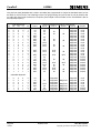
Versions
Release
V 1.7
V 1.8
V 1.9
V 2.0
Date
Dec 13th, 1999
April 10th 2002
Sept. 19th 2002
Oct 31st 2002
Changes
Chapter 3.1
Chapter 3.1, Block Diagram
Housing dimensions
Chap 6: “Technical Data” because manufacturer has
changed from NI to NEC
User Description
Copyright (C) Siemens AG 2002. All rights reserved.
Release V2.0
Page 3
10/2002
ComDeC
LSPM2
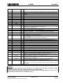
Table of Contents
1
INTRODUCTION
6
2
OVERVIEW OF FUNCTIONS
7
3
PIN DESCRIPTION
8
4
5
3.1
XTAL1, XTAL2 crystal oscillator connection
10
3.2
FQ48
10
3.3
RWCONS
11
3.4
ACA (AddressChangeAllowed)
11
3.5
XSREE
11
3.6
DIAERROR
12
3.7
NORMOPER
12
3.8
XTRI
12
3.9
XTEMO-Pin
12
FUNCTION DESCRIPTION OF THE INDIVIDUAL BLOCKS
13
4.1
Watchdog timer
13
4.2
Automatic baud rate detection
13
4.3
EEPROM interface (serial)
4.3.1
EEPROM parameters
4.3.2
EEPROM interface
4.3.3
EEPROM control
14
14
15
16
4.4
Shift register interface
4.4.1
Shift register parameters
4.4.2
Shift register interface
4.4.3
Control of the external shift register
17
17
18
18
4.5
I/O interface
4.5.1
Structure of the diagnostic ports
19
21
4.6
PROFIBUS DP interface
22
TELEGRAM STRUCTURE
24
5.1
Parameter telegram (SET_PARAM)
24
5.2
Diagnostic telegram (SLAVE_DIAG)
26
5.3
Configuration telegram (GET_CONFIG)
28
Page 4
10/2002
Release V2.0
User Description
Copyright (C) Siemens AG 2002. All rights reserved.
LSPM2
ComDeC
5.4
Optional services
28
5.5
Other services
28
TECHNICAL DATA
29
6
Maximum limit values
Permitted operating ratings
DC specification of the I/O driver
7
29
29
29
TIMINGS
34
7.1
EEPROM
34
7.2
Shift register
36
7.3
RESET
36
7.4
Consistency signal RWCONS
37
8
ADDRESS DIRECTORY
38
9
CIRCUIT EXAMPLES
39
9.1
Shift register
39
9.2
Wiring example - EEPROM , ext. oscillator , error indicator and RESET
40
9.3
Wiring Example - PROFIBUS Interface
41
10
BUS CONNECTION
User Description
Copyright (C) Siemens AG 2002. All rights reserved.
42
Release V2.0
Page 5
10/2002
ComDeC
LSPM2
1 Introduction
Siemens offers its users some ASICs which support resp. fully handle data communication between the
individual automation stations for simple and fast digital data exchange between programmable logic
controllers.
The SPC 3 is a PROFIBUS DP slave. It supports passive users on the bus system and filters off all external
telegrams and errored wanted telegrams.
However, there are also simple devices, such as switches and thermocouples, in the field of automation
which do not require a microprocessor for detection of their states.
A further ASIC with the designation LSPM2 (Lean Siemens Profibus Multiplexer) is available for low-cost
adaptation of these devices. The LSPM2 operates as a Slave in the bus system. A Master addresses the
LSPM2 via Layer 2 of the 7-Layer Model. After the LSPM2 has received an error-free telegram, it
automatically generates the requested response telegrams (in accordance with IEC 61158).
Page 6
10/2002
Release V2.0
User Description
Copyright (C) Siemens AG 2002. All rights reserved.
LSPM2
ComDeC
2 Overview of functions
The LSPM2 has input/output ports which can be adapted directly to the periphery for data exchange with the
periphery. The function blocks which the LSPM2 contains include the following:
The UART converts the parallel data of the I/O ports to a serial data stream for the DP bus and vice versa.
The BAUD RATE GENERATOR generates baud rates of 9.6 kBd to 12 MBd. The clock for the baud rate
generator can be supplied either by an external, connected crystal oscillator or by an external clock pulse
generator.
Two operating modes are possible:
-48 MHz clock and baud rates of 9.6 kBd to 12 MBd
-24 MHz clock and baud rates of 9.6 kBd to 6 MBd
The IDLE timer generates the bus idle time which is required for synchronising the listening users.
The integrated watchdog timer monitors the users present for addressability. In the event of an error, all ports
are set to logical “0” in order to avoid malfunctions.
The I/O interface contains four input/output ports and one diagnostic port. The ports each have a width of
eight bits. Two input/output ports can be configured as additional diagnostic ports by selecting a special
operating mode.
The micro-sequencer (MS) performs the task of handling telegram communication and evaluating the
individual functions, including automatic baud rate detection.
The USER interface state machine generates control signals for the MS and generates the status indication
which the Master can request for evaluation.
The Profibus DP-specific parameters (station address and ID number) may be stored in external EEPROM or
in a serial shift register. The interface configuration (input or output) is set via five pins on the LSPM2. An
integrated control logic generates the signals for controlling the serial EEPROM or external shift register
independently, depending on the external wiring used.
User Description
Copyright (C) Siemens AG 2002. All rights reserved.
Release V2.0
Page 7
10/2002
ComDeC
LSPM2
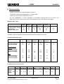
3 Pin description
The LSPM2 has an 80-pin QFP package (QFP80-P-1420B, Plastic Rectangular Flat Package) with the
following signal pins:
PIN
Signal name
I/O
1
XCTS
I
2
3
4
5
6
7
RXD
RTS
TXD
VSS
PA0
PA1
I
O
O
8
9
10
11
12
13
14
15
16
17
18
PA2
PA3
PA4
PA5
VSS
PA6
PA7
VDD
PB0
PB1
PB2
I/O
I/O
I/O
I/O
19
20
21
22
23
24
25
26
27
PB3
PB4
PB5
PB6
PB7
VSS
VDD
PE0
PE1
I/O
I/O
I/O
I/O
I/O
28
29
30
31
32
33
34
35
36
37
38
39
PE2
PE3
PE4
PE5
VSS
VDD
PE6
PE7
VSS
PC0
PC1
PC2
I
I
I
I
40
41
42
43
44
45
PC3
PC4
PC5
PC6
PC7
VDD
Page 8
10/2002
I/O
I/O
Function
ClearToSend; PROFIBUS interface: The LSPM2 is Clear To Send if the XCTS signal is
active
ReadData; PROFIBUS interface: input/receive data for LSPM2
RequestToSend: The LSPM2 requests Clear to Send with RTS=´1´
TransmitData; PROFIBUS interface: Output or transmit data from LSPM2
Data port A; can be programmed with parameters as an input or output port, depending
on the
setting at the type inputs 0..4 (see Configuration Table I/O interface)
I/O
I/O
I/O
I/O
I/O
I
I
Data port B; can be programmed with parameters as an input or output port, depending
on the
setting at the type inputs 0..4 (see Configuration Table I/O interface)
Diagnostic port E; the LSPM2 receives diagnostic information of the programmable data
ports
or user-specific diagnosis via this port
I
I
I/O
I/O
I/O
I/O
I/O
I/O
I/O
I/O
Data port C; can be programmed with parameters as input, output or diagnostic port,
depending
on the setting at the type inputs 0..4 (see Configuration Table I/O interface)
Release V2.0
User Description
Copyright (C) Siemens AG 2002. All rights reserved.
LSPM2
PIN
Signal name
I/O
46
47
PD0
PD1
I/O
I/O
48
49
50
51
52
53
54
55
56
57
PD2
PD3
PD4
PD5
VSS
PD6
PD7
VDD
XRESET
RWCONS
I/O
I/O
I/O
I/O
58
59
60
XTEMO
XTRI
XSREE
I
I
I
61
62
63
FQ48
DIAERROR
NORMOPER
I
O
O
64
65
66
67
68
69
70
71
72
73
74
75
VSS
TYP0
TYP1
TYP2
TYP3
TYP4
VSS
XTAL2
XTAL1
VDD
VSS
ACA
76
INTERCLK
O
77
INTERCS
O
78
INTERDI
I
79
INTERDOD
O
80
VDD
ComDeC
Function
Data port D; can be programmed with parameters as input, output or diagnostic port,
depending
on the setting at the type inputs 0...4 (see Configuration Table I/O interface)
I/O
I/O
I
O
I
I
I
I
I
O
I
I
Asynchronous Reset input; resets the LSPM2 to a defined initial state
ReadWriteCONSistent; output ´Read or Write Consistent´; signal for “pre-announcing” a
following write or read access operation on the data ports;
(see the Annex for signal timing)
Apply log<1> permanently to test pin (normal mode)
Apply log<1> permanently to test pin (normal mode)
Defines whether an external EEPROM or an external shift register (parallel in, ser.out) is
connected to the LSPM2;
log<1> ext. EEPROM, log<0>ext. shift register
Operating frequency select pin log<1> 48 MHz; log<0> 24 MHz
DIAgnosisERROR; this output is set when external diagnosis occurs
NORMalOPERation; operating state indicator
log<1> if parameter assignment telegram has been received with DA=TS (not in the case
of broadcast tel.)
log<0> after RESET and after each timeout of the WD timers
Type setting; the data ports (A-D) of the LSPM2 are programmed with these 5 pins;
number of ports used, use as input or output ports, with/without consistency,
extended diagnosis
(see Configuration Table I/O interface)
Oscillator output (see Wiring example)
Oscillator input
(see Wiring example)
AddressChangeAllowed; with ACA signal active, it is possible, with the corresponding call
telegram, to overwrite the EEPROM contents even with No_Add_Chg bit.
INTERfaceCLocK; depending on pin XSREE, the LSPM2 generates clock sequences for
the external EEPROM or external shift register via this signal.
INTERfaceChipSelect; depending on pin XSREE, the LSPM2 selects the external
EEPROM or
external shift register via this signal.
INTERfaceDataInput; LSPM2 receives input data from the external EEPROM
or external shift register, depending on pin XSREE, via this channel.
INTERfaceDataOutloaD; depending on pin XSREE, this output serves as a data channel
to
the EEPROM or as a data accept signal (parallel load) for loading data into the external
shift register.
Important:
The Pins for Type settings are only allowed to be changed when the ASIC is without voltage.
Dynamical change of the Type settings while working is not permitted.
When switching on the power (voltage rise) the output RTS of the ASIC may be set. This is to be
compensated by external wiring. See RESET wiring.
User Description
Copyright (C) Siemens AG 2002. All rights reserved.
Release V2.0
Page 9
10/2002
ComDeC
LSPM2
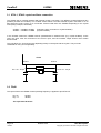
3.1 XTAL1, XTAL2 crystal oscillator connection
The LSPM2 has an internal oscillator with external crystal connection. Two different crystal frequencies are
possible (24 MHz and 48 MHz). The 24 MHz version allows a 24 MHz external crystal connection or a 48
MHz harmonic-mode crystal to be connected. Various baud rates are available depending on the crystal
used (wiring example, see below).
24 MHz -- 9.6 kBd to 6 MBd
48 MHz -- 9.6 kBd to 12 MBd
(external crystal connection or crystal oscillator)
(crystal oscillator)
In the 48 MHz version the LSPM2 must be operated with an external clock (e.g. crystal oscillator). In this
case, the clock must be connected to the XTAL1 input, and the oscillator output XTAL2 must remain
disconnected.
The real values for Cin and Cout are depending mainly on the layout and the crystal . They must be
calculated for every circuit separately.
LSPM2
XTAL1
XTAL2
R2=1M
Cin =10 ...30 pF
Cout= 10 ...30 pF
3.2 FQ48
This input informs the LSPM2 of what operating frequency is applied to pins XTAL1/2.
log.<0>
log. <1>
24 MHz
48 MHz
The input must be wired.
Page 10
10/2002
Release V2.0
User Description
Copyright (C) Siemens AG 2002. All rights reserved.
LSPM2
ComDeC
3.3 RWCONS
This output signal serves to pre-announce a consistent write or read access operation on the data ports.
Timing for this is described in Chapter 7.4.
3.4 ACA (AddressChangeAllowed)
With ACA signal active, it is possible, with a corresponding call telegram, to overwrite the EEPROM contents
even with No_Add_Chg bit set (see Telegram structure, Chapter 5.).
log. <1> active TS address can be overwritten in the EEPROM
If the LSPM2 is operated with a shift register, this input does not function.
A defined level must be applied to the pin.
Attention: After Power on you can always overwrite the adress.
3.5 XSREE
This input defines whether the LSPM2 is operated with an external EEPROM or external shift register.
log. <0>
log. <1>
ext. shift register
ext. EEPROM
The input must be wired.
User Description
Copyright (C) Siemens AG 2002. All rights reserved.
Release V2.0
Page 11
10/2002
ComDeC
LSPM2
3.6 DIAERROR
This output serves to signal a diagnostic error and can be used to activate an LED. The output driver power is
4 mA.
log.<0>
log.<1>
no diagnostic error
diagnostic error, i.e. a log.<0> is applied to one of the diagnostic ports
Note: See Chapter 4.5 for further information on diagnosis.
3.7 NORMOPER
This output indicates the operating state of the LSPM2 on the Profibus DP and can be used to activate an
LED. The output driver power is 4 mA.
log.<0>
log.<1>
after Reset and each time after timeout of the watchdog timer
if a parameter assignment telegram destination address (DA) = station address (TS)
has been received, i.e. if communication has been established with Master
(Data-Exchange mode).
3.8 XTRI
Note: A defined level must be applied to all inputs.
VDD must be applied to the XTRI pin in normal mode.
3.9 XTEMO-Pin
Note: Defined levels must be applied to all inputs.
VDD must be applied to the XTEMO pin in normal mode.
Page 12
10/2002
Release V2.0
User Description
Copyright (C) Siemens AG 2002. All rights reserved.
LSPM2
ComDeC
4 Function description of the individual blocks
4.1 Watchdog timer
If malfunctions or disturbances occur on the bus line, it may be the case that the LSPM2 does not receive a
telegram and, thus, the module’s ports can no longer be operated. A WD is integrated in order to detect this
situation. The WD timer is used initially for automatic baud rate detection after Reset.
When the correct baud rate has been detected, the MS switches the WD timer automatically to normal mode
(Watchdog mode).
If WD mode is enabled, the timer is reset with each error-free telegram received, on recognition of the station
number.
If a timeout of the timer occurs, i.e. no valid telegram detected, all outputs are reset ("0") and the system
branches automatically to the automatic baud rate detection function.
The timeout time can be programmed in the COM-ET200. It is possible to select a value between 2 ms and
650 s, regardless of the set baud rate, thus permitting adaptation to the relevant system conditions.
The watchdog timeout times which can be set are calculated as follows:
T(WD) = factor * WD_1 * WD_2
Time factors 1 ms or 10 ms can be set via the parameter
assignment telegram in the User_Prm_Data (see Telegram
structure, Chapter 5.).
Setting WD_1=WD_2=1 is not permitted. In addition, neither WD_1 nor WD_2 may be 0!
4.2 Automatic baud rate detection
The LSPM2 is capable of detecting the baud rate automatically. The MS reverts automatically to the
automatic baud rate detection function after each RESET and after WD timer timeout. No ports are
manipulated during detection.
The MS always starts detection of the set baud rate with the highest baud rate and works through each baud
rate sequentially until it has received any SD1 or SD2 telegram with no errors. This telegram may be routed
to any user.
After detection of the correct baud rate, the MS reverts to normal mode (Watchdog mode).
Important: After false configuration or setting the bit UNLOCK in the parameter telegram, the LSPM2
returns to state WAIT_PRM, but doesn`t go to SEARCH BAUDRATE any more. This could make
problems by changing the baudrate at the master at this moment.
Important: If the LSPM2 gets in state DATA_EXCHANGE a data telegram with more output bytes than
selected at the ASIC, the LSPM2 answers with RS, but the ASIC remais in state DATA_EXCHANGE.
User Description
Copyright (C) Siemens AG 2002. All rights reserved.
Release V2.0
Page 13
10/2002
ComDeC
LSPM2
4.3 EEPROM interface (serial)
4.3.1 EEPROM parameters
The LSPM2 integrates a controller for a serial ext. EEPROM. Only one 16-bit word is ever stored as the
parameter (EEPROM address 0H) or only two 16-bit words are ever read as the parameter (address
00H,01H).
Assignment EEPROM word 0
15
14
13
12
11
0
0
0
0
0
Assignment EEPROM word 1
15
14
13
12
11
X
X
X
X
X
10
9
0
0
10
9
X
X
8
7
6
5
0
No Ad
d_Chg
X
X
8
7
ID number
X
X
4
3
2
TS address
X
X
X
1
0
X
X
6
5
4
3
2
1
0
X
X
X
X
X
X
X
The ID number must be written to the EEPROM before connecting to the LSPM2 since only the TS
address can be changed during write access via the LSPM2. Both data words are accessed only
during read operations, i.e. an EEPROM programmed with the ID number must be used for
production of a unit.
Attention: After Power on you can always overwrite the adress.
ID number:
The ID number serves as a unique identification of a DP Slave device type on the bus. An ID number is
required for all DP Slave devices when reading diagnostic data, when writing parameter assignment data and
when changing the station address via the bus. The ID number makes is possible for the DP Masters to
identify the DP Slaves with minimal protocol effort.
An individual ID number is issued by the PNO (PROFIBUS User Organisation) for each device type. This ID
number is not a serial number. Once a manufacturer has received an ID number for a device type from the
PNO, he may use this number for each device of this type produced without having to ask for an ID number
again each time from the PNO.
A separate ID number does not need to be applied for each revision level of devices which are basically
identical but which differ as regards the number of inputs and outputs. The precondition is that the product
can be described as a modular device in the GSD (device master file).
During the boot phase or after a RESET, the LSPM2 accepts the parameters (word 0, word 1) serially from
an EEPROM and loads them into its internal parameter register.
The following values are permitted:
TS address:
ID number:
1....
126D
all 16-bit values (as assigned by the PNO)
If the LSPM2 detects an illegal address (0 or 127D) when reading in, the MS automatically writes the default
value TS=126D and No_Add_Chg=0 to the EEPROM. This permits parameter assignment of the station
address with the corresponding tool (COM ET200).
Page 14
10/2002
Release V2.0
User Description
Copyright (C) Siemens AG 2002. All rights reserved.
LSPM2
ComDeC
4.3.2 EEPROM interface
The EEPROM control logic contained in the LSPM2 supports only serial modules with 5V supply, 16-bit
organisation and integrated control logic. The control signals for EEPROMs with designation 93C46/47 are
compatible EEPROMs (e.g. type OKI Datacode 16811 or higher) are generated. An ERASE/WRITE ENABLE
cycle precedes each write cycle since the module is generally in DISABLE state after a power failure or power
fade (i.e. it cannot be erased or written).
The LSPM2 internally triggers a write/read cycle with two flags (RD-EEPROM and WR-EEPROM),
whereupon the EEPROM controller generates the corresponding control sequences for the output pins.
When the cycle is completed, the controller acknowledges this by resetting the flags.
Signal name
I/O
Function
INTERCS
INTERCLK
INTERDI
O
O
I
INTERDOD
O
Chip-select for EEPROM
Clock signal for EEPROM
DATA IN (Read EEPROM) (ST), READY
after programming
Data Out (Write EEPROM)
Status after
RESET XSREE=“1”
log. <0>
log. <0>
log. <0>
ST = Schmitt trigger
After the micro-sequencer (MS) has issued a read request to the controller, the read data is stored in a shift
register and acknowledged by resetting the RD flag.
When writing the memory, the MS loads the data of the station address directly into the shift register of the
EEPROM controller, provided the telegram has been received error-free by the LSPM2. During the write
operation, the MS continues normal program processing. As soon as the memory chip has accepted the
data, the controller acknowledges this by resetting the WD flag. If the LSPM2 receives a request to write the
EEPROM, it acknowledges reception of the call telegram and then branches to the baud rate detection
function.
A RESET during writing leads to undefined data in the EEPROM.
User Description
Copyright (C) Siemens AG 2002. All rights reserved.
Release V2.0
Page 15
10/2002
ComDeC
LSPM2
4.3.3 EEPROM control
Since the memory has a serial interface, the data, addresses and also the commands for switching over to
the various operating modes must be transferred to it serially. The specified module awaits a 2-bit Op code
after a start bit (log. "1") and then a 6-bit address, i.e. 9 bits, in order to switch to the corresponding mode.
Data is read or written only after this.
The following Op codes are generated:
Command
Start bit/Opcode
READ WORD
ERASE/WRITE-ENABLE
WRITE WORD
110
100
101
Address (binary)
000000 bzw. 000001
110000
000000
An erase cycle is not required since the memory overwrites the corresponding word when writing.
The word with address 000 000Bin is generally addressed in the EEPROM, but an Erase/Write-Enable cycle is
executed before each write access operation since the module is generally in Erase/Write-Disable mode after
the power is restored.
The integrated controller of the LSPM2 generates a clock (INTERCLK) and a Chip-Select signal (INTERCS)
with the corresponding timing and clocks the control bits and data out sequentially when writing or into an
internal shift register when reading.
min. 4µs
INTERCLK
Clock for EEPROM
internal clock
min. 2µs
A read access operation takes 200 µs for one complete read cycle. A write cycle requires 100 µs, in addition
to the programming time of approx. 10 ms per word.
Note: See Chapter 8 for a circuit example of connection of an EEPROM.
Page 16
10/2002
Release V2.0
User Description
Copyright (C) Siemens AG 2002. All rights reserved.
LSPM2
ComDeC
4.4 Shift register interface
Besides the option of connecting an external EEPROM, the LSPM2 can also be wired with an external shift
register (XSREE=0). In this case, the integrated shift register controller independently generates control
sequences for shift registers with designation 74HC165 or compatible shift registers.
4.4.1 Shift register parameters
The internal shift register of the LSPM2 is written serially via bit position 23. The data are shifted to the right
depending on the number of clock pulses still pending, i.e. the contents of position 23 are stored in bit 22, and
the contents of position 22 are stored in bit 21 etc.
The following data sequence must be observed in this case at the serial data input (INTERDI):
first bit 0 (TS address) then bit 1 TS , bit 2 TS, bit 3 ...........bit 0 ID no, bit 1 ID no.,......etc.
Shift direction of the internal shift register (LSPM2)
23 22 21 20 19 18 17 16 15 14 13 12 11 10 9 8 7 6 5 4 3 2 1 0
74HC165
external
shift
register
ID number
INTERDI
Serial
data input 7
LSPM2
6 5
High
4 3 2 1
Low
TS address
BCD-coded
0 7 6 5 4 3 2 1 0 7 6 5 4 3 2 1 0
BCD-BINARY convertor
(internal)
16
7
16 bit ID number
TS-Adresse, binary coded
A total of 24 bits must be stored in the external shift register: 16 bits for the ID number and 8 bits for
the TS address.
The TS address must be set BCD-coded externally (values permitted are 1Dec to 99Dec). If the LSPM2
detects the illegal value 0Dec, the TS address is assigned 126Dec.
The externally set address is converted BCD-BINARY in the LSPM2 in order to permit the Slave
address (TS) to be compared with the binary-coded destination address (DA) of the call telegram.
User Description
Copyright (C) Siemens AG 2002. All rights reserved.
Release V2.0
Page 17
10/2002
ComDeC
LSPM2
4.4.2 Shift register interface
The shift register controller is a block which is independent of the rest of the module and which is triggered
only by the micro-sequencer (MS). The MS triggers a read cycle with a ReadShift flag, whereupon the shift
register controller generates the corresponding control sequences for the interface pins. When the read cycle
is complete, the controller acknowledges this by resetting the ReadShift flag.
If an external shift register is connected, the sequencer issues a read request to the controller after a
RESET in order to accept the data in its parameter register.
Signal name
I/O
Function
INTERCS
INTERCLK
INTERDI
INTERDOD
O
O
I
O
Clock Enable for shift register
Clock signal for shift register
DATA IN (Read shift register), (ST)
Accept signal for data to external
shift register. (parallel load)
Status after
RESET XSREE=“0”
log. <1>
log. <0>
log. <1>
ST=Schmitt trigger
4.4.3 Control of the external shift register
The sequential control generates a clock (INTERCLK), a Clock Enable signal (INTERCS) and an Accept
signal (INTERDOD) with the required timing and clocks the data sequentially into an LSPM2-internal shift
register when reading.
When reading, the data is first loaded in parallel into the external shift register with the INTERDOD signal.
From there, the data is clocked serially into the LSPM2-internal shift register (see Chapter Timing for timing).
min. 4µs
INTERCLK
Clock for shift register
internal clock
min. 2µs
The shift register controller operates with the same clock frequency as the EEPROM controller, i.e. 250 kHz.
A read access operation takes 96 µs.
Note: See Chapter 8 for a circuit example.
Page 18
10/2002
Release V2.0
User Description
Copyright (C) Siemens AG 2002. All rights reserved.
LSPM2
ComDeC
4.5 I/O interface
The following ports are available to the user for detection and output of the various signals of a process
sequence on site:
− two programmable 8-bit input/output ports (port A, port B
− two programmable 8-bit ports (port C, port D) which can be configured optionally as input/output
ports or as additional diagnostic ports for recording errors.
− one 8-bit user-specific diagnostic port (port E
The various I/O configuration can be set via the parameter pins (type 0 to type 4), and the coding of the
individual configuration is specified in the table below. In the case of “extended diagnosis”, bit-serial diagnosis
for data ports A and/or D can be performed for instance via the diagnostic ports C and/or D. Port E is still
available as an additional diagnostic port.
Attention: Please confirm that the Typ Pins are always set if Power off.
When using consistency the master documentations has to be attended!
Bei “erweiterter Diagnose” kann über die Diagnoseports C und/oder D z.B. bitweise Diagnose für die
Datenports A und/oder B durchgeführt werden, Port E steht dabei weiterhin als zusätzlicher Diagnoseport zur
Verfügung.
User Description
Copyright (C) Siemens AG 2002. All rights reserved.
Release V2.0
Page 19
10/2002
ComDeC
LSPM2
The ports not used (identified with a dash in the table) are programmed as outputs as standard and must not
be wired on the PC board. The advantage of this over programming as inputs is that no pull-up resistors and
no pads with internal pull resistors are required. (See Chapter Technical Data for the characteristic data of
the input/output ports.)
Type assignment
<3> <2> <1>
0
0
0
0
0
0
0
0
1
0
0
1
0
1
0
0
1
0
0
1
1
0
1
1
1
0
0
1
0
0
1
0
1
1
0
1
1
1
0
1
1
0
1
1
1
1
1
1
0
1
0
0
1
1
0
1
1
1
0
0
1
0
0
1
1
0
1
1
0
1
1
1
1
1
1
<4>
0
0
0
0
0
0
0
0
0
0
0
0
0
0
0
0
1
1
1
1
1
1
1
1
1
<0>
0
1
0
1
0
1
0
1
0
1
0
1
0
1
0
1
1
0
1
0
1
0
1
0
1
Port A
IN
IN
IN
IN
OUT
OUT
OUT
OUT
OUT
OUT
OUT
OUT
OUT
OUT
IN
IN
OUT
OUT
OUT
IN
OUT
OUT
OUT
0
1
0
1
0
0
1
IN
IN
OUT
OUT
OUT
IN
OUT
Port configuration/consistency requirement
Port B
Port C
Port D
Port E
Diagnosis
IN
Diagnosis
IN
IN
Diagnosis
IN
IN
IN
Diagnosis
Diagnosis
IN
Diagnosis
IN
IN
Diagnosis
IN
IN
IN
Diagnosis
OUT
Diagnosis
OUT
IN
Diagnosis
OUT
IN
IN
Diagnosis
Diagnosis
OUT
OUT
Diagnosis
OUT
OUT
IN
Diagnosis
Diagnosis
OUT
OUT
OUT
Diagnosis
IN
Diagnosis
IN
IN
IN
Diagnosis
OUT
Diagnosis
OUT
OUT
OUT
Diagnosis
OUT
IN
IN
Diagnosis
IN
IN
Diagnosis
OUT
OUT
Diagnosis
OUT
OUT
IN
Diagnosis
IN
IN
IN
Diagnosis
Consist.
none
none
none
none
none
none
none
none
none
none
none
none
none
none
none
none
overall
overall
overall
overall
overall
overall
overall
overall
overall
extended diagnosis:
1
1
1
1
1
1
1
0
0
0
0
0
1
1
Page 20
10/2002
0
0
0
0
1
0
0
0
0
1
1
0
1
1
IN
OUT
IN
IN
OUT
Release V2.0
Diagnosis
Diagnosis
Diagnosis
Diagnosis
Diagnosis
Diagnosis
Diagnosis
Diagnosis
Diagnosis
Diagnosis
Diagnosis
Diagnosis
Diagnosis
Diagnosis
Diagnosis
Diagnosis
Diagnosis
Diagnosis
Diagnosis
none
none
none
none
none
overall
overall
User Description
Copyright (C) Siemens AG 2002. All rights reserved.
LSPM2
ComDeC
4.5.1 Structure of the diagnostic ports
The group diagnostic port (port E) is available to the user as a user-specific diagnostic port with 8 bits in any
configuration. Two operating modes are basically possible for this port, and these operating modes can be
set by the user with the parameter fag ENA_SAMMEL_DIA (see Telegram structure, Chapter 5.)
Flag=log.<0>
log<0> at a pin of port E leads to a DIA_ERROR (DIAERROR output is set to log.<1>)
Flag=log.<1>
Errors at pins E0 to E3 set the DIA_ERROR only if a channel diagnostic error is also pending
at port C or port D.
An error at pins E4 to E7 always leads to a DIA_ERROR. (Regardless of ports C and D).
If programmed via the type pins, the LSPM2 also has two channel diagnostic ports (ports C and D) which it
can use to monitor each of the I/O ports (ports A and B). If ports D and E are set as diagnostic ports, a
log.<0> at one of the pins always leads to a DIA_ERROR which is forwarded in the LSPM2 internally as
log.<1>.
The channel diagnostic ports can also be masked channel-by-channel (each bit) via mask registers. After a
Reset, all masks are inactive. An error (log.<0>) at a channel diagnostic port is forwarded only if the
corresponding mask bit is equal to zero (see also Chapter 5 Telegram structure SET_PARAM).
However, the user can also use all diagnostic ports for user-specific diagnosis. A log. <0> at a diagnostic
input corresponds to a diagnostic error and sets the output pin DIA-ERROR on the LSPM2 to log. <1>.
Output DIA-ERROR remains set until an error level is no longer applied to the diagnostic ports. The pin can
be used to drive an LED. The driver power of the output is 4 mA.
In order to prevent unwired inputs of external diagnostic hardware leading permanently to a DIA_ERROR, the
LSPM2 has an internal logic. This logic compares the current diagnostic data with the data last read in and
generates an error only if a diagnostic change has occurred, i.e. each change is sent to the Master only once.
+5V must be applied via pull-up resistors to all unused inputs of the group diagnostic port and the
programmed channel diagnostic port.
User Description
Copyright (C) Siemens AG 2002. All rights reserved.
Release V2.0
Page 21
10/2002
ComDeC
LSPM2
4.6 PROFIBUS DP interface
Transmission is performed in operating mode RS485 (RS485 physical).
Der LSPM2 hat hierfür folgende Pins:
Signal name
I/O
Type
RTS
TXD
RXD
XCTS
O
O
I
O
CMOS
CMOS
CMOS
CMOS
Function
Request to Send
Transmit data
Receive data
Clear to Send
Before sending, the LSPM2 sets the RTS signal to "1" and then loads the transmit buffer of the UART with
the 1st character. The UART delays the first telegram character until signal CTS is active. CTS is no longer
polled during telegram transmission. On completion of transmission (buffer empty stop bit is send), the RTS
is reset. The XCTS pin must be set to log.<0> during operation.
Switching times:
No.
Symbol
Parameter
1
TsRTS (TXD) RTS ↑ to TXD (Setup-Time)
2
ThRTS (TXD) RTS ↓ to TXD (Hold-Time)
*: 1 Tbit = 104µs at 9,6kBd, 1 TBit = 83ns at 12MBd
min.
Unit
2
2
TBit*
TBit*
Timing:
RTS
2
1
TXD
Attention:
At Power on is it possible that the RTS signal is a short moment high. You must consider this in your
application (see circuit diagramm).
Page 22
10/2002
Release V2.0
User Description
Copyright (C) Siemens AG 2002. All rights reserved.
LSPM2
ComDeC
The DP interface is designed as in 9-pin SUB D connector with the following pin assignment:
Pin 1 - not used
Pin 2 - not used
Pin 3 - B line
Pin 4 - Request to Send (RTS)
Pin 5 - Ground 5V (M5)
Pin 6 - 5V potential (P5 floating approx. 100 mA)
Pin 7 - not used
Pin 8 - A line
Pin 9 - not used
The line screen must be connected to the housing.
The supported current on PIN 6 depends on the connected device
Bus termination inside of the connector acc. to IEC 61158
app. 10 mA
ET200 Handheld:
app. 50 mA
Optical bus terminal
:
app. 90 mA
The pin assignment of the free pins can be used optionally in accordance with IEC 61158.
Note: See Chapter 8 for a circuit example.
User Description
Copyright (C) Siemens AG 2002. All rights reserved.
Release V2.0
Page 23
10/2002
ComDeC
LSPM2
5 Telegram structure
The LSPM2 is a passive Slave user of PROFIBUS-DP. Required response telegrams are generated by the
LSPM2 independently as soon as it has received a telegram destined for it free of errors from the Master.
Telegram communication between Master and Slave has been kept simple and forms only a subset of the
possible PROFIBUS telegrams.
In “normal mode” the LSPM2 processes only error-free SD1 or SD2 telegrams (StartDelimiter with
value 10HEX or 68HEX) directed to it (correct TS address). Other telegrams are filtered. One exception is
baud rate detection mode in which the LSPM2 can receive all telegrams (including SD3 and SD4
telegrams). However, it does not evaluate these telegrams but triggers only baud rate detection.
Only special features of the telegrams which it is essential to observe when using an LSPM2 Slave are
described below.
5.1 Parameter telegram (SET_PARAM)
The Master transfers parameter assignment data to the LSPM2 with this telegram. 5 bytes USER parameter
data must be transferred to the LSPM2 in addition to the 7 parameter bytes.
Byte
7
6
5
0
0
0
Bit position
4
3
Designation
2
1
0
0
0
6
7
0
EN_
Sammel_
Dia
WD_
Base
User_Def_PRM1
8
Mask for Diaport1
9
Mask for Diaport2
10
0
0
0
0
0
0
0
0
User_Def_PRM2
11
0
0
0
0
0
0
0
0
User_Def_PRM3
Page 24
10/2002
Release V2.0
User Description
Copyright (C) Siemens AG 2002. All rights reserved.
LSPM2
ComDeC
Byte 0-6: Parameter assignment data, see IEC 61158
Byte 7:
User_Def_PRM1
Bit 0,1: are reserved and must be set to 0
Bit 2:
The WD base bit defines the timebase with which the watchdog is clocked
´0´= timebase 10 ms (status after Reset)
´1´= timebase 1 ms
Bit 3:
This bit activates group diagnostic mode.
EN_Sammel_Dia = 0
EN_Sammel_Dia = 1
A channel diagnostic error of port D and E is always signalled.
An error at pins E0-E3 is signalled to the Master only if a channel
diagnostic error also occurs.
Error changes at the channel diagnostic ports and pins E4-E7 of
the group diagnostic port are, however, still forwarded
immediately.
IMPORTANT: If a type configuration without channel diagnosis (port C and D) is
set, EN_Sammel_Dia must be programmed as 0!
Bit 4-7: are reserved and must be set to 0
Byte 8, 9,: Mask bytes for diagnostic ports
Byte 8 contains the mask bits for diagnostic byte 1 (port C) and byte 9 contains the mask bits for
diagnostic byte 2 (port D). The mask bits are assigned to the corresponding bit positions of the
diagnostic ports. A ´1´ at the corresponding bit position masks diagnosis, i.e. these bits are
masked. All masks are cleared after Reset.
IMPORTANT: If a type configuration without diagnosis is set, the mask bits must be
programmed as 00HEX!
Byte 10, 11: User_Def_PRM2/3
These bytes are currently not yet used for checking purposes and must be set to ´0´.
User Description
Copyright (C) Siemens AG 2002. All rights reserved.
Release V2.0
Page 25
10/2002
ComDeC
LSPM2
5.2 Diagnostic telegram (SLAVE_DIAG)
The LSPM2 sends diagnostic data to the Master with this telegram. A ´1´ at a bit position signifies that the
corresponding event has occurred.
A further 7 bytes of external diagnostic data, described in the following table, are sent by the LSPM2, in
addition to the 6 bytes diagnostic data. Diagnostic data is transferred only after a change of the pending data.
One exception to this is Freeze mode.
IMPORTANT: If Freeze mode is activated, the diagnostic data is also frozen. A telegram is thus sent
to the Master not with a change in diagnostic data but only after a further ´Freeze´.
Byte
Bit position
4
3
7
6
5
6
0
0
0
0
7
PE7
PE6
PE5
8
0
0
9
PC7
10
Designation
2
1
0
0
1
1
1
PE4
PE3
PE2
PE1
PE0
0
0
0
0
0
0
PC6
PC5
PC4
PC3
PC2
PC1
PC0
PD7
PD6
PD5
PD4
PD3
PD2
PD1
PD0
11
0
0
0
0
0
0
0
0
Diag_Reserved_2
12
0
0
0
0
0
0
0
0
Diag_Reserved_3
5
Page 26
10/2002
Release V2.0
Diag_Header
Port diagnosis (port
E)
Diag_Reserved_1
Port C (only with
extended diagnosis,
otherwise 00HEX)
Port D (only with
extended diagnosis,
otherwise 00HEX)
User Description
Copyright (C) Siemens AG 2002. All rights reserved.
LSPM2
ComDeC
Byte 6: Diag_Header
This byte contains the LSPM2-specific number of external diagnostic bytes, i.e. value 07HEX is entered
at this point on the LSPM2.
Byte 7: Group diagnosis
This byte contains the diagnostic data of the signals pending at port E. A diagnostic error at one of the
pins (log.<0>) is forwarded inverted, i.e. the error is indicated with ´1´ at the corresponding bit position.
Byte 8, 11, 12: Diag_Reserved
These bytes are reserved. The LSPM2 always sends value 00HEX at this point.
Byte 9, 10: channel diagnosis port C, port D
This byte contains the diagnostic data of the signals pending at port C and port D. A diagnostic error at
one of the pins (log.<0>) is forwarded inverted, i.e. the error is indicated with ´1´ at the corresponding
bit position. If no extended diagnosis is set via the type coding, value 00HEX is always entered at this
point.
User Description
Copyright (C) Siemens AG 2002. All rights reserved.
Release V2.0
Page 27
10/2002
ComDeC
LSPM2
5.3 Configuration telegram (GET_CONFIG)
The Master transfers the configuration data to the LSPM2 with this telegram. The LSPM2 always expects 2
code bytes. The following sequence must be observed.
Byte
Bit position
4
3
7
6
5
0
0/1
0
1
0
1
0/1
0
0
1
Byte 0: Code byte_Outputs
Following values permitted:
Byte 1: Code byte_Inputs
Following values permitted:
Designation
2
1
0
0
0
0/1
0/1
Code byte_Outputs
0
0
0/1
0/1
Code byte_Inputs
without consistency
20Hex with 1 output
21Hex with 2 outputs
22Hex with 3 outputs
23Hex with 4 outputs
00Hex with 0 outputs
Overall consistency
A0Hex with 1 output
A1Hex with 2 outputs
A2Hex with 3 outputs
A3Hex with 4 outputs
00Hex with 0 outputs
without consistency
10Hex with 1 input
11Hex with 2 inputs
12Hex with 3 inputs
13Hex with 4 inputs
00Hex with 0 inputs
Overall consistency
90Hex with 1 input
91Hex with 2 inputs
92Hex with 3 inputs
93Hex with 4 inputs
00Hex with 0 inputs
5.4 Optional services
The LSPM2 basically supports SYNC and FREEZE mode, i.e. if a SYNC or FREEZE is set in the
Global_Contol_Service, this function is executed.
Note: If FREEZE mode is activated, the diagnostic data is also frozen. A change is not signalled to the
Master until a further FREEZE is transmitted.
5.5 Other services
The LSPM2 supports services Set_Slave_Adress (if using a serial EEPROMs), Read_Inputs, Read_Outputs,
Get_Config.
Page 28
10/2002
Release V2.0
User Description
Copyright (C) Siemens AG 2002. All rights reserved.
LSPM2
ComDeC
6 Technical data
LSPM2 = Lean Siemens Profibus Multiplexer Version 2.
LSPM2 (NEC): New device. Manufacturer is company NEC.
LSPM2 (TI): The old device. Manufacturer was TI.
The new LSPM2(NEC) is 100% compatible in functionality compared with the TI version. The
differences are only concerning the electrical specification shown in the different tables below.
Maximum limit values
Parameter
Design
ation.
VDD
Supply Voltage
Inp Voltage/Outp. Voltage VI/Vo
II
Input Current
TStg
Storage Temperature
Min.NEC
Version
- 0.5
- 0.5
k.A.
-65
Min TI
Version
Vss –0,3
Vss –0,3
-10
-40
Max.NEC
Version
6.0
VDD + 0.5
+20
+150
Max TI
Version
7
VDD + 0.3
10
125
Unit
V
V
mA
ο
C
Important: Long-term operation with these values reduces the module’s service life.
Permitted operating ratings
Parameters
Supply Voltage
Input High Voltage
Input Low Voltage
Designatio
n.
VDD
VIHC
VILC
Min.NEC
Version
4.5
0.7 VDD
0.00
Min TI
Version
4,75
3,5
k.A.
Max.NEC
Version
5.5
VDD
0.3 VDD
Max. TI
Version
5,25
Unit
1,5
V
V
V
Schmitt-Trigger:
(CMOS)
Input High Voltage
Input Low Voltage
Hysteresis Voltage
Vp
Vn
Vh
2.85
1.15
1.3
4
k.A.
k.A.
3.75
1.75
2.07
k.A.
1
k.A.
V
V
V
(TTL)
Input High Voltage
Input Low Voltage
Hysteresis Voltage
Vp
Vn
Vh
1.68
0.64
0.83
4
k.A
k.A
2.55
1.33
1.44
k.A.
1
k.A
V
V
V
DC specification of the I/O driver
Parameters
Design Condition
Condition
ation NEC Version TI Version
VOH
IOH = 0 mA
k.A.
Output High
Voltage
VOL
IOL = 0 mA
k.A.
Output Low
Voltage
User Description
Copyright (C) Siemens AG 2002. All rights reserved.
Min
NEC
VDD – 0.1
0,4
Release V2.0
Min
TI
k.A.
0,4
Max
NEC Vers.
k.A:
k.A.
Max
TI Vers.
Vdd –0,8
Unit
k.A.
V
V
Page 29
10/2002
ComDeC
LSPM2
Signal line
Driver type
PA(7:0) bis PD(7:0)
TXD
RTS
NORMOPER
DIAERROR
INTERCLK
INTERCS
INTERDOD
RWCONS
XTAL2
Power of driver
NEC Version
6 mA
9 mA
9 mA
6 mA
6 mA
6 mA
6 mA
6 mA
6 mA
6 mA
6 mA
Tristate
Tristate
Tristate
Tristate
Tristate
Tristate
Tristate
Tristate
Tristate
Tristate
Buffer
Power of driver
NI Version
4 mA
8 mA
8 mA
4 mA
4 mA
4 mA
4 mA
4 mA
4 mA
4 mA
4 mA
Pins of the LSPM2
Inputs:
ACA
FQ48
PE7...0
INTERDI
RXD
XTEMO
XTRI
XSREE
TYP4...0
CTS
XRESET
XTAL1
Anz.
1
1
8
1
1
1
1
1
5
1
1
1
I/O
IN
IN
IN
IN
IN
IN
IN
IN
IN
IN
IN
IN
LEVEL
CMOS
CMOS
CMOS
TTL
CMOS
CMOS
CMOS
CMOS
CMOS
CMOS
CMOS
Outputs:
DIAERROR
INTERCLK
INTERCS
INTERDOD
NORMOPER
RWCONS
RTS
TXD
XTAL2
Anz. I
1
1
1
1
1
1
1
1
1
I/O
OUT
OUT
OUT
OUT
OUT
OUT
OUT
OUT
OUT
CMOS
CMOS
CMOS
CMOS
CMOS
CMOS
CMOS
CMOS
CMOS
Bidirektionale Pins:
PA7...0
PB7...0
PC7...0
PD7...0
Anz.
8
8
8
8
I/O
I/O
I/O
I/O
I/O
CMOS
CMOS
CMOS
CMOS
Art
Normal
Normal
Schmitt-Trigger
Schmitt-Trigger
Schmitt-Trigger
Normal
Normal
Normal
Normal
Schmitt-Trigger
Schmitt-Trigger
Buffer
Art
Buffer
6 mA-Buffer
6 mA-Buffer
6 mA-Buffer
6 mA-Buffer
6 mA-Buffer
6 mA-Buffer
9 mA-Buffer
9 mA-Buffer
6 mA-Buffer
Art
Schmitt-Trigger
Schmitt-Trigger
Schmitt-Trigger
Schmitt-Trigger
Buffer
6 mA-Buffer
6 mA-Buffer
6 mA-Buffer
6 mA-Buffer
Power supply
7 VDD / 9 VSS
________________________________
Total
Page 30
10/2002
80 Pins
Release V2.0
User Description
Copyright (C) Siemens AG 2002. All rights reserved.
LSPM2
User Description
Copyright (C) Siemens AG 2002. All rights reserved.
Release V2.0
ComDeC
Page 31
10/2002
ComDeC
LSPM2
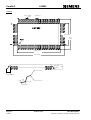
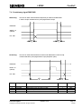
Housing
0.37 +0.08
-0.07
0.8 (T .P.)
14.0 +-0.2
17.2
+-0.2
20.0 +-0.2
23.2 +-0.2
2.7+ 0.1
3,0
1.6 +-0.2
0,17
+0.08
-0.07
0° - 10°
0,8 +/- 0,2
Page 32
10/2002
Release V2.0
User Description
Copyright (C) Siemens AG 2002. All rights reserved.
LSPM2
ComDeC
Information on handling:
The ESD safety measures must always be observed on all electronic components.
The LSPM2-ASIC is a component subject to the risk of cracking and must be handled accordingly.
The LSPM2 must be dried before processing. The component must be dried for 24 hours at 125oC
and then processed within a period of 48 hours. This drying process may be carried out only once
owing to component solderability. Also ensure that the pins of the LSPM2 are not bent. Proper
processing can be guaranteed only if the deviation from flatness is less than 0.1 mm. The LSPM2ASIC is approved for infrared soldering with soldering profile in accordance with CECC00802.
User Description
Copyright (C) Siemens AG 2002. All rights reserved.
Release V2.0
Page 33
10/2002
ComDeC
LSPM2
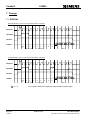
7 Timings
7.1 EEPROM
EEPROM READ cycle Op code 10 (example address 000 000b)
1
INTERCLK
INTERDOD
INTERCS
INTERDI
Startbit
1
2
1
2-bit Op code
2
3
4
5
6
Data
6-bit address
EEPROM READ cycle Op code 10 (example address 000 001b)
1
INTERCLK
INTERDOD
INTERCS
INTERDI
Startbit
1
Page 34
10/2002
min. 2µs
1
2
2-bit Op code
1
2
3
6-bit address
4
5
6
Data
The controller switches the signals to the pins with the trailing edge.
Release V2.0
User Description
Copyright (C) Siemens AG 2002. All rights reserved.
User Description
Copyright (C) Siemens AG 2002. All rights reserved.
Release V2.0
min. 2us
INTERDI
INTERCS
INTERDOD
INTERCLK
1
Startbit
1
2
2
2-bit Op code
01
1
2-bit Op code
00
1
1
1
3
3
6-bit address
000 000
2
6-bit address
110 000
2
4
4
5
5
6
6
D15
D14
The controller switches the signals to the pins with the trailing edge.
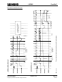
Startbit
EEPROM WRITE cycle
INTERCS
INTERDOD
INTERCLK
1
EEPROM ERASE/WRITE cycle
Data
D13
D0
Programming time
(max. 10ms)
3*SC
READY
Waiting for READY
The Write cycle follows
without interruption.
LSPM2
ComDeC
EEPROM ERASE/WRITE-Zyklus
Page 35
10/2002
ComDeC
LSPM2
7.2 Shift register
Shift register READ cycle
1
INTERCLK
INTERDOD
(par. load)
INTERCS
(clock enable)
INTERDI
D0
D1
D2
D3
D4
D5
D20
D21
D22
D23
Data
Data bit : D0 - D7 TS address
D8 - D23 PNO ID number
1
min. 2us
The controller switches the signals to the pins with the trailing edge.
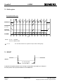
7.3 RESET
XRESET
min. 20 clock pulses
( =416ns at 48MHz )
A spike filter is integrated upstream of the reset logic. This filter filters noise spikes up to a length of
one clock pulse in order to prevent interference on the RESET line.
Page 36
10/2002
Release V2.0
User Description
Copyright (C) Siemens AG 2002. All rights reserved.
LSPM2
ComDeC
7.4 Consistency signal RWCONS
Write timing:
The user can switch external latches transparently for instance with RWCONS
in order to accept new data from the ports programmed to Output.
RWCONS
WRITE - IO
(internal)
Port data
1
Read timing:
2
The user can freeze external latches for instance with RWCONS in order to accept
consistent data at the ports programmed to Input ("Snapshot" option).
RWCONS
READ - IO
(internal)
Port data
3
No.
Symbol
4
Parameter
1
RWCONSSETUP
RWCONS activ to Write from MS
2
RWCONSHOLD
RWCONS inactiv to Write from MS
3
DSETUP
Data - Setup after RWCONS active
4
DHOLD
Data - Hold after RWCONS inactiv
*: 1 TBit =104µs at 9,6kBd , 1 TBit = 83ns at 12MBd
User Description
Copyright (C) Siemens AG 2002. All rights reserved.
Release V2.0
Unit
1
1
1
0
TBit*
TBit*
TBit*
ns
Page 37
10/2002
ComDeC
LSPM2
8 Address Directory
Technical reference partners in the interface center
Siemens AG
A&D SE RD 73
Hr. Putschky
Internal address:
Würzburgerstr.121
90766 Fürth
Tel.: (0911) 750 -
2078
Fax (0911) 750 -
2100
Page 38
10/2002
Release V2.0
User Description
Copyright (C) Siemens AG 2002. All rights reserved.
77
INTERCS
76
INTERCLK
79
INTERDOD
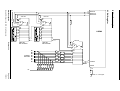
74HC165
G1
C2
2
1 1
15
C3/
1
74HC165
G1
C2
2
1 1
15
C3/
1
10
11
12
13
14
3
4
5
6
10
3D
11
2D
12
2D
13
14
3
4
5
6
3D
2D
2D
LSPM2
9
7
Release V2.0
LSPM2
9
7
330R
330R
1
1
74HC165
G1
C2
2
1 1
C3/
15
1
1
HIGH - byte
PNO - ID number
LOW - byte
PNO - ID number
Bit 7
Bit 6
Bit 5
TS address Bit 4
BCD coded Bit 3
Bit 2
Bit 1
Bit 0
15K
15K
15K
15K
15K
15K
15K
3K3
3K3
3K3
3K3
3K3
3K3
3K3
15K
3K3
9 Circuit examples
9.1 Shift register
User Description
Copyright (C) Siemens AG 2002. All rights reserved.
M
10
11
12
13
14
3
4
5
6
3D
2D
2D
9
7
78
INTERDI
XSREE
60
330R
Page 39
10/2002
XSREE <0> = Shift register
M
ComDeC
P5
ComDeC
LSPM2
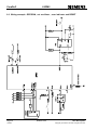
9.2 Wiring example - EEPROM , ext. oscillator , error indicator and RESET
Page 40
10/2002
Release V2.0
User Description
Copyright (C) Siemens AG 2002. All rights reserved.
User Description
Copyright (C) Siemens AG 2002. All rights reserved.
RXD
TXD
CTS
RTS
Release V2.0
2
M
P5
P5
4
1
300R
20K
68n
M
68n
680R
M
300R
OUT
680R
68n
68n
2.2 .. 22nF
500 V
680R
680 R
2
1M
2M
2P5
2M
2P5
&
74HC132
Layout :lines must be kept as short as possible.
U-
IN
UEN
U+
U+
U-
EN
OUT
U+
HCPL7101
U-
IN
U+
HCPL7101
EN
HCPL0601
300 R
1K 2
w irin g e xa m p le
2M
2P5
1K2
2
EN2
GND
EN1
U+
1
1
75ALS176D
Shield
6
7
Driver select :
Differential voltage > 2V
1
2
5
3
8
Important: electrical isolation to bus
P5 and 2P5
680R
68n
2P5
300R
100 K
se e re se t
2M
100 K
3
A-line
2P5
2M
RTS
B-line
9
8
7
6
5
4
3
2
1
LSPM2
ComDeC
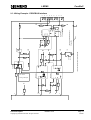
9.3 Wiring Example - PROFIBUS Interface
Page 41
10/2002
ComDeC
LSPM2
10 Bus Connection
The bus can be connected using the following standard connectors, amongst others, in accordance with
PROFIBUS-DP Standard:
MLFB-No.
6ES7 972 - 0BA00 - 0XA0
6ES7 972 - 0BB00 - 0XA0
Notes
without PG gland
with PG gland
Colour of the connector housing
anthracite
anthracite
Dimension drawings:
DP bus connector: 6ES7 972 0BA00- 0XA0
Page 42
10/2002
Release V2.0
User Description
Copyright (C) Siemens AG 2002. All rights reserved.
LSPM2
ComDeC
DP bus connector: 6ES7 972 - 0BB00 - 0XA0
The slide switch on the rear side of the bus connector must be set to position “ON” in order to connect the
bus terminating resistor.
Lines A and B of the incoming and outgoing bus cable must each be connected via separate screw-type
terminals.
User Description
Copyright (C) Siemens AG 2002. All rights reserved.
Release V2.0
Page 43
10/2002