1
UM1079
User manual
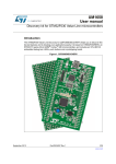
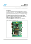
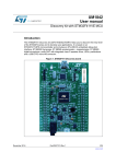
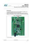
STM32L-DISCOVERY
Introduction
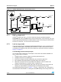
The STM32L-DISCOVERY helps you to discover the STM32L ultralow power features and
to develop and share your applications. It is based on an STM32L152RBT6 and includes an
ST-LINK/V2 embedded debug tool interface, LCD (24 segments, 4 commons), LEDs,
pushbuttons, a linear touch sensor, and four touchkeys.
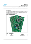
Figure 1.
June 2011
STM32L-DISCOVERY board
Doc ID 018789 Rev 2
1/35
www.st.com
Contents
UM1079
Contents
1
Conventions . . . . . . . . . . . . . . . . . . . . . . . . . . . . . . . . . . . . . . . . . . . . . . . . 4
2
Quick start . . . . . . . . . . . . . . . . . . . . . . . . . . . . . . . . . . . . . . . . . . . . . . . . . 5
2.1
Getting started . . . . . . . . . . . . . . . . . . . . . . . . . . . . . . . . . . . . . . . . . . . . . . 5
2.2
System requirements . . . . . . . . . . . . . . . . . . . . . . . . . . . . . . . . . . . . . . . . . 6
2.3
Development toolchain supporting the STM32L-DISCOVERY . . . . . . . . . 6
2.4
Demonstration software . . . . . . . . . . . . . . . . . . . . . . . . . . . . . . . . . . . . . . . 6
2.5
Order code . . . . . . . . . . . . . . . . . . . . . . . . . . . . . . . . . . . . . . . . . . . . . . . . . 6
3
Features . . . . . . . . . . . . . . . . . . . . . . . . . . . . . . . . . . . . . . . . . . . . . . . . . . . 7
4
Hardware and layout . . . . . . . . . . . . . . . . . . . . . . . . . . . . . . . . . . . . . . . . . 8
4.1
STM32L152RBT6 microcontroller . . . . . . . . . . . . . . . . . . . . . . . . . . . . . . 11
4.2
Embedded ST-LINK/V2 . . . . . . . . . . . . . . . . . . . . . . . . . . . . . . . . . . . . . . 13
4.2.1
Using the ST-LINK/V2 to program/debug the STM32L on board . . . . . . 14
4.2.2
Using the ST-LINK/V2 to program/debug an external
STM32L application . . . . . . . . . . . . . . . . . . . . . . . . . . . . . . . . . . . . . . . . 15
4.3
Power supply and power selection . . . . . . . . . . . . . . . . . . . . . . . . . . . . . . 16
4.4
LEDs . . . . . . . . . . . . . . . . . . . . . . . . . . . . . . . . . . . . . . . . . . . . . . . . . . . . 16
4.5
Pushbuttons . . . . . . . . . . . . . . . . . . . . . . . . . . . . . . . . . . . . . . . . . . . . . . . 17
4.6
Linear touch sensor/touchkeys . . . . . . . . . . . . . . . . . . . . . . . . . . . . . . . . . 17
4.7
Built-in IDD measurement circuit . . . . . . . . . . . . . . . . . . . . . . . . . . . . . . . 17
4.7.1
High IDD range mode . . . . . . . . . . . . . . . . . . . . . . . . . . . . . . . . . . . . . . . 18
4.7.2
Low IDD range mode . . . . . . . . . . . . . . . . . . . . . . . . . . . . . . . . . . . . . . . 18
4.7.3
IBIAS current measurement procedure . . . . . . . . . . . . . . . . . . . . . . . . . . 19
4.8
Solder bridges . . . . . . . . . . . . . . . . . . . . . . . . . . . . . . . . . . . . . . . . . . . . . 20
4.9
LCD (24 segments, 4 commons) . . . . . . . . . . . . . . . . . . . . . . . . . . . . . . . 22
5
Extension connectors . . . . . . . . . . . . . . . . . . . . . . . . . . . . . . . . . . . . . . . 24
6
Mechanical drawing . . . . . . . . . . . . . . . . . . . . . . . . . . . . . . . . . . . . . . . . 27
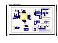
7
Electrical schematics . . . . . . . . . . . . . . . . . . . . . . . . . . . . . . . . . . . . . . . 28
2/35
Doc ID 018789 Rev 2
UM1079
8
Contents
Revision history . . . . . . . . . . . . . . . . . . . . . . . . . . . . . . . . . . . . . . . . . . . 34
Doc ID 018789 Rev 2
3/35
Conventions
1
UM1079
Conventions
Table 1 provides the definition of some conventions used in the present document.
Table 1.
ON/OFF conventions
Convention
4/35
Definition
Jumper JP1 ON
Jumper placed between pin 2 and 3
Jumper JP1 OFF
Jumper placed between pin 1 and 2
Solder bridge SBx ON
SBx connections closed by solder
Solder bridge SBx OFF
SBx connections left open
Doc ID 018789 Rev 2
UM1079
2
Quick start
Quick start
The STM32L-DISCOVERY is a low-cost and easy-to-use development kit to quickly
evaluate and start a development with an STM32L ultralow power microcontroller.
Before installing and using the product, please accept the Evaluation Product License
Agreement from www.st.com/stm32l-discovery.
For more information on the STM32L-DISCOVERY and for demonstration software visit
www.st.com/stm32l-discovery.
2.1
Getting started
Follow the sequence below to configure the STM32L-DISCOVERY board and launch the
DISCOVER application:
1.
Check jumper positions on the board: JP1 and CN3 must be ON (Discovery selected)
(see Figure 3 on page 9).
2.
Connect the STM32L-DISCOVERY board to a PC with a USB cable to power the
board. Red LED LD2 (PWR) and LD1 (COM) are then lit up.
3.
Function 1 is executed. Each click on user button B1 changes the executed function as
described in Table 2 on page 5.
A 4-LED bar shows the function being performed (1 to 4 bars can be switched ON).
Depending on the function selected, the voltage value, the linear touch sensor position, the
touchkey status, or the STM32L current consumption is displayed on the LCD.
Table 2.
Functions executed when clicking B1 button
Function LED LD3/4
Bar
status
Value displayed on LCD
1
LD3 and
LD4 blink
Measured STM32L VDD voltage
2
LD3 ON
Linear touch sensor position from 0 to 100%
3
LD4 ON
Status of the 4 touchkeys
Main function
Voltage
measurement
Touch sensing
STM32L consumption measured in Run mode (4 MHz)
4
STM32L consumption measured in Sleep mode (4 MHz)
STM32L consumption measured in Run mode (32 KHz)
5
LD3 and
LD4 OFF
STM32L consumption measured in low power sleep mode
(32 KHz)
STM32L consumption measured in Stop mode, RTC ON
STM32L current
consumption
measurement
6
STM32L consumption measured in Stop mode, RTC OFF
7
STM32L consumption measured in Standby mode
Doc ID 018789 Rev 2
5/35
Quick start
UM1079
To study or modify the DISCOVER project related to this demonstration, visit
www.st.com/stm32l-discovery and follow the tutorial. Discover the STM32L features,
download and execute programs proposed in the list of projects. This site also contains
examples from which you can develop your own applications.
2.2
2.3
2.4
System requirements
●
Windows PC (2000, XP, Vista, 7)
●
USB type A to Mini-B USB cable
Development toolchain supporting the STM32L-DISCOVERY
●
Altium TASKING™ VX-Toolset
●
Atollic TrueSTUDIO?
●
IAR EWARM
●
Keil™ MDK-ARM
Demonstration software
The demonstration software is preloaded in the board Flash memory. It uses the built-in IDD
measurement feature of the STM32L-DISCOVERY to automatically measure and display on
the LCD the MCU consumption in Run and low power modes.it also allows to demonstrate
touch sensing functionalities such as linear touch sensor or touchkeys.
The latest versions of this demonstration source code and associated documentation can
be downloaded from www.st.com/stm32l-discovery.
2.5
Order code
To order the STM32L ultralow power discovery board, use the order code STM32LDISCOVERY.
6/35
Doc ID 018789 Rev 2
UM1079
3
Features
Features
The STM32L-DISCOVERY offers the following features:
●
STM32L152RBT6 microcontroller, featuring 128 KB of Flash memory, 16 KB of RAM,
4 KB of data EPROM, in a 64-pin LQFP package
●
On-board ST-LINK/V2 with selection mode switch to use the kit as a standalone STLINK/V2 (with SWD connector for programming and debugging)
●
Board power supply: through USB bus or from an external 3.3 or 5 V supply voltage
●
External application power supply: 3 V and 5 V
●
IDD current measurement
●
LCD
●
–
DIP28 package
–
24 segments, 4 commons
Four LEDs:
–
LD1 (red/green) indicating USB communication
–
LD2 (red) indicating that 3.3 V power supply is ON
–
Two user LEDs, LD3 (green) and LD4 (blue)
●
Two pushbuttons (user and reset)
●
One linear touch sensor and four touchkeys
●
Extension header for LQFP64 I/Os for quick connection to prototyping board and easy
probing
Doc ID 018789 Rev 2
7/35
Hardware and layout
4
UM1079
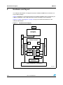
Hardware and layout
The STM32L-DISCOVERY is designed around the STM32L152RBT6 microcontroller in a
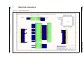
64-pin LQFP package.
Figure 2 illustrates the connections between the STM32L152RBT6 and its peripherals (STLINK/V2, pushbutton, LED, LCD, linear touch sensor, touchkeys, and connectors).
Figure 3 on page 9 and Figure 4 on page 10 help you to locate these features on the
STM32L-DISCOVERY.
Figure 2.
Hardware block diagram
-INI
53"
37$
%MBEDDED
34,).+6
34-,2"4
)/
)/
2%3%4
'REEN,%$
,$
"
234
"LUE,%$
,$
"
53%2
(EADER
(EADER
)/
)$$
-EASUREMENT
,INEARTOUCHSENSOR
TOUCHKEYS
,#$3EGMENTS#OMMONS
-36
8/35
Doc ID 018789 Rev 2
UM1079
Hardware and layout
Figure 3.
Top layout
,$
#/-
#.
37$CONNECTOR
,$
072
34,).+6
#.34,).+$)3#/6%29
SELECTOR
6POWER
SUPPLYINPUTOUTPUT
6POWER
SUPPLYINPUTOUTPUT
,#$
SEGMENTS
)$$MODULE
3"
)$$MEASUREMENT
*0
)$$MEASUREMENT
3""//4
34-,24
*066"!4SELECTOR
OPTIONALNOTMOUNTED
3"
"53%2
3"
"2%3%4
"
RESETBUTTON
"
USERBUTTON
,$
BLUE,%$
,$
GREEN,%$
,INEARTOUCHSENSOR
TOUCHKEYS
-36
1. Pin 1 of CN1, CN2, P1 and P2 connectors are identified by a square.
Doc ID 018789 Rev 2
9/35
Hardware and layout
Figure 4.
UM1079
Bottom layout
3"3"3"3"
RESERVED
3".234
3"34-?234
3"3"3"3"
DEFAULT
3"37/
0CONNECTOR
0CONNECTOR
3")$$
MEASUREMENT
*0)$$
3"3"
8CRYSTAL
3""//4
3"-#
3"3"
8CRYSTAL
3"
6$$POWEREDFROM6
3"
"ATTERYENABLE
#2
BATTERYHOLDER
OPTIONAL
-36
1. Pin 1 of CN1, CN2, P1 and P2 connectors are identified by a square.
10/35
Doc ID 018789 Rev 2
UM1079
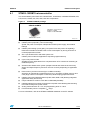
4.1
Hardware and layout
STM32L152RBT6 microcontroller
This 32-bit ultralow power MCU has 128 KB Flash, 16 KB RAM, 4 KB data EEPROM, RTC,
LCD, timers, USART, I2C, SPI, ADC, DAC and comparators.
Figure 5.
STM32L152RBT6 package
34-,2"4
+BYTESOF&LASHMEMORY
+BYTESOF2!+BYTESOFDATA%%02/-
,1&0XMM
-36
This device provides the following benefits:
●
Ultralow power proprietary 130 nm technology:
Speed and power consumption independent of MCU power supply, and ultralow
leakage
●
Ultralow power design (clock gating, low-power Flash with power-off capability):
Reduced overall Run and Wait mode current consumption by turning off clocks of
unused peripherals or Flash
●
Sub 1 µA hardware RTC and AWU system unit:
Ultralow power modes for applications requesting regular wake up
●
Up to 6 low power modes:
Suitable for many applications from complete switch off to continuous monitoring at
ultralow frequency
●
Advanced and flexible clock system (multiple internal and external clock sources)
Switch and adjust frequency and clock sources on the fly depending on application
needs
●
Direct memory access on board (up to 12 DMA channels):
Autonomy for peripherals, independent from core; can switch off Flash memory and
CPU (large current consumption contributors) while keeping peripherals active
●
Ultralow power and ultrasafe features (POR, PDR, BOR, PVD) allowing integrated
application safety and security
●
Unique identifier to enhance user data confidentiality/reliability
●
Ultrafast wakeup from lowest consumption low-power mode allowing fast switching
from static and dynamic power modes
●
Analog functional down to 1.8 V, and programming down to 1.65 V
●
Full functionality over the complete VDD range
For more information, refer to the STM32L152RBT6 datasheet on the ST website.
Doc ID 018789 Rev 2
11/35
Hardware and layout
Figure 6.
UM1079
STM32L152RBT6 block diagram
42!#%#+42!#%$
42!#%$42!#%$
42!#%$
6$$
*4!'37
4RACECONTROLLER
%4-
PBUS
&LASH OBL
)NT ERFACE
#ORTEX-#05
)BUS
&MAX -(Z
-05
$BUS
3YST EM
.6)#
'0$-!
!("0#,+
!0"0#,+
(#,+
&#,+
6$$!
"/262%&).4
6$$!
633!
06$
84!,/3#
-(Z
CLOCK
MANAGEMENT
2#-3
/3#?).
/3#?/54
)7$'
2#,3
)NT
#OMP
#/-0?). ).
6$$!
0,,
2#(3
0OWERRESET
#OMP
0OWERUP
0OWERDOWN
3TANDBYINTERFACE
6$$!
!("& MAX -(Z
62%&/54054
3UPPLY
MONITORING
6$$ 6TO6
633
+"&LASH
+"DATA%%02/-
2!- +"
CHANNELS
.234
0/7%2
6/,4 2%'
"US-ATRIX
.*4234
*4$)
*4#+37#+
*4-337$
*4$/
AS!&
6#/2%
84!,K(Z
24#
!75
"ACKUP
REGISTER
/3#?).
/3#?/54
3YNC(Z
24#?!&
0!;=
'0)/!
0";=
'0)/"
0#;=
'0)/#
0$;=
'0)/$
4)-
#HANNELS
0%;=
'0)/%
4)-
#HANNELS
0(;=
'0)/(
4)-
#HANNELS
6,#$
"ACKUPINTERFACE
!&
%84)4
7+50
-/3)-)3/
3#+.33AS!&
30)
!&
6$$2%&?!$#
53!24
6$$!
BIT!$#
6332%&?!$#
)&
4EMPS ENSOR
'ENERALPURPOSE
TIMERS
#HANNE LS
!0" &MAX -(Z
2848#43243
3MART#ARDAS!&
!("
!0"
!0"& MAX -(Z
!("
!0"
,#$STEPUP
CONVERTER
53"2!-"
53!24
2848#43243
3MART#ARDAS !&
53!24
2848#43243
3MART#ARDA S!&
30)
-/3)-)3/3#+.33
AS!&
)#
3#,3$!
AS!&
)#
3#,3$!3-"US0-"US
AS!&
53"&3DEVICE
77$'
,#$XX
"!3)#4)-%23
6,#$6TO6
53"$0
53"$3%'X
#/-X
6$$!
4)-
4)-
#HANNEL
4)-
#HANNEL
4)-
BIT$!#
$!#AS!&
BIT$!#
$!#AS!&
)&
)&
4)-
-
AIE
12/35
Doc ID 018789 Rev 2
UM1079
4.2
Hardware and layout
Embedded ST-LINK/V2
The ST-LINK/V2 programming and debugging tool is integrated on the STM32LDISCOVERY. The embedded ST-LINK/V2 can be used in 2 different ways according to the
jumper states (see Table 3 on page 13):
●
Program/debug the MCU on board,
●
Program/debug an MCU in an external application board using a cable connected to
SWD connector CN2.
The embedded ST-LINK/V2 supports only SWD for STM32 devices. For information about
debugging and programming features refer to user manual UM1075 which describes in
detail all the ST-LINK/V2 features.
Figure 7.
Typical configuration
(ARDWAREREQUIREMENTS
53"CABLETYPE!TOMINI"
COMPUTERWITH7INDOWS806ISTAOR
$EVELOPMENTTOOLCHAIN
!LTIUM4!3+).'684OOLSET
!TOLLIC4RUE345$)/
)!2%7!2+EIL-$+!2-
-36
Table 3.
Jumper states
Jumper state
Description
Both CN3 jumpers ON
ST-LINK/V2 functions enabled for on board programming
(default)
Both CN3 jumpers OFF
ST-LINK/V2 functions enabled for external application through
CN2 connector (SWD supported).
Doc ID 018789 Rev 2
13/35
Hardware and layout
4.2.1
UM1079
Using the ST-LINK/V2 to program/debug the STM32L on board
To program the STM32L on board, simply plug in the two jumpers on CN3, as shown in
Figure 8 in red, but do not use the CN2 connector as that could disturb communication with
the STM32L152RBT6 of the STM32L-DISCOVERY.
Figure 8.
STM32L-DISCOVERY connections image
0INOF#.
37$CONNECTOR
#.JUMPERS/.
-36
14/35
Doc ID 018789 Rev 2
UM1079
4.2.2
Hardware and layout
Using the ST-LINK/V2 to program/debug an external
STM32L application
It is very easy to use the ST-LINK/V2 to program the STM32L on an external application.
Simply remove the 2 jumpers from CN3 as shown in Figure 9, and connect your application
to the CN2 debug connector according to Table 4.
Note:
SB100 must be OFF if you use CN2 pin 5 in your external application.
Table 4.
Figure 9.
Debug connector CN2 (SWD)
Pin
CN2
Designation
1
VDD_TARGET
VDD from application
2
SWCLK
SWD clock
3
GND
Ground
4
SWDIO
SWD data input/output
5
NRST
RESET of target MCU
6
SWO
Reserved
ST-Link connections image
0INOF#.
37$CONNECTOR
#.JUMPERS/&&
Doc ID 018789 Rev 2
15/35
Hardware and layout
4.3
UM1079
Power supply and power selection
The power supply is provided either by the host PC through the USB cable, or by an external
5 V or 3.3 V power supply.
The D1 and D2 protection diodes allow the EXT_5V and EXT_3V pins to be used
independently as input or output power supplies (see Figure 3 on page 9):
●
EXT_5V and EXT_3V can be used as output power supplies when the application
board is connected to pins P1 and P2. In this case, the EXT_5V and EXT_3V pins
deliver a 5 V or 3 V power supply and power consumption must be lower than 100 mA.
●
EXT_5V and EXT_3V can also be used as input power supplies e.g. when the USB
connector is not connected to the PC. In this case, the STM32L-DISCOVERY board
must be powered by a power supply unit or by auxiliary equipment complying with
standard EN-60950-1: 2006+A11/2009, and must be Safety Extra Low Voltage (SELV)
with limited power capability.
Battery powered (optional)
In addition, the STM32L-DISCOVERY board has been designed to run from a CR2032
standalone battery (no connection with USB or other power supply is required).
By default, no battery holder is mounted on the board and SB21 and SB22 are configured in
their default state (see Table 5: Solder bridges on page 20).
Follow the procedure below to power the STM32L-DISCOVERY from the battery:
1.
Solder a B7410AP2L battery holder from LOTES on CR1.
2.
Configure SB100 OFF.
3.
Remove both jumpers from CN3 (see Figure 9)
4.
Select the battery as power supply. Two solutions are possible:
a)
Solder bridge: Configure SB21 OFF, and SB22 ON. No header is required on JP2.
b)
Jumper: Configure SB21 and SB22 OFF.
Solder a header on JP2, identical to JP1 on the top side, and set a jumper
between VDD and VBAT to power the STM32L MCU.
Note:
In this configuration, it is possible to power the STM32L from the board 3 V supply voltage
by setting a jumper between VDD and 3V.
5.
Plug the CR2032 battery into CR1 holder. You can now run the demonstration.
Warning:
4.4
16/35
Wrong solder bridge configuration can damage board
components.
LEDs
●
LD1 COM: LD1 default status is red. LD1 turns to green to indicate that
communications are in progress between the PC and the ST-LINK/V2.
●
LD2 PWR: red LED indicates that the board is powered.
●
User LD3: green LED is a user LED connected to the I/O PB7 of the STM32L152RBT6.
●
User LD4: blue LED is a user LED connected to the I/O PB6 of the STM32L152RBT6.
Doc ID 018789 Rev 2
UM1079
4.5
4.6
Hardware and layout
Pushbuttons
●
B1 USER: User pushbutton connected to the I/O PA0 of the STM32L152RBT6.
●
B2 RESET: Pushbutton is used to RESET the STM32L152RBT6.
Linear touch sensor/touchkeys
To demonstrate touch sensing capabilities, the STM32L-DISCOVERY includes a linear
touch sensor which can be used either as a 3-position linear touch sensor or as 4
touchkeys. Both functionalities are illustrated in the demonstration software (see Table 2:
Functions executed when clicking B1 button on page 5).
3 pairs of I/O ports are assigned to the linear touch sensor/touchkeys. Each pair must
belong to the same analog switch group:
●
PA6, PA7 (group 2)
●
PC4, PC5 (group 9)
●
PB0, PB1 (group 3)
To minimize the noise, these pairs are dedicated to the linear touch sensor and the
touchkeys and are not connected to external headers.
To design a touch sensing application, refer to the following documentation and firmware:
4.7
●
For details concerning I/O ports, refer to the STM32L152RBT6 datasheet.
●
For information on software development, see DISCOVER application software on
http://www.st.com/stm32l-discovery.
●
For more detail concerning touch sensing application design and layout, refer to
AN2869 -Guidelines for designing touch sensing applications.
●
STM32 touch sensing library available from http://www.st.com/stm32l-discovery.
Built-in IDD measurement circuit
The STM32L-DISCOVERY built-in IDD measurement circuit allows the consumption of the
STM32L152RBT6 to be measured and displayed on the LCD Glass while the MCU is in Run
or low power modes.
Note:
●
JP1 ON: STM32L152RBT6 is powered through the IDD measurement circuit (default).
●
JP1 OFF: STM32L152RBT6 is directly powered, IDD measurement circuit is bypassed.
When jumper JP1 is removed the current consumption of the STM32L152RBT6 can be
measured by connecting an ammeter between jumper pin 1 and pin 2 of JP1.
For IDD measurement to be performed by the MCU itself, the circuit below is implemented
on the STM32L-DISCOVERY. Solder bridges SB1, SB2 and SB14 must be closed and JP1
must be ON.The low IDD range procedure (see Section 4.7.2) is recommended when the
MCU is in low power mode and the IDD current does not exceed 60 μ A. When the MCU
operates in Run mode and can sink up to 30 mA, use the high IDD range procedure (see
Section 4.7.1).
Doc ID 018789 Rev 2
17/35
Hardware and layout
UM1079
Figure 10. STM32L-DISCOVERY IDD measurement circuit
)$$ -EASURE
6$$?-#5
ON
OFF
*0
2
+
6$$
3
'
3
'
3"
$
$
$
$
)$$?-EASUREMENT
2
+
#
U&
6$$
3"
0! 2
+
6$$
#
N&
5
)$$?7!+%50
5
,8'#42
6$$
5
2
('342
6$$
2
5
-! 8&%5+ 5
)/
/)
#
'.$ 6##
0! 1 6##
1
1
1
1
1
1
1
#,2
1
#)
1
#/
'.$
#/
-(#442
343$0&,
6$$
2
+
)$$?#.4?%.
3"
#
N&
2
+
0#
2
+
/SCILLATOR FREQUENCY +(Z
-36
4.7.1
High IDD range mode
In high IDD range mode, the IDD current is measured using the operational amplifier
MAX9938FEUK+ (U5) connected to the 2 Ω shunt resistor (R21). In this case IDD_CNT_EN
remains high during measurement, so R22 remains in short-circuit during the measurement
because FET transistor 1 of U20 remains ON permanently.
4.7.2
Low IDD range mode
In low IDD range mode, the operational amplifier MAX9938FEUK+ (U5) is connected to the
1 KΩ shunt resistor (R22), controlled by FET transistor 1 of U20. In this case the counter
74HC4060 (U3) enabled by IDD_CNT_EN manages the measurement timing according to
Figure 11 on page 19.
Low IDD range measurement principle
The principle used to measure the consumption current when the STM32L152RBT6 is in
low IDD range mode is as follows:
1.
Configure ADC to measure voltage on the IDD_Measurement pin.
2.
Configure PA0 to serve as wakeup pin.
3.
Enter low IDD range mode after setting IDD_CNT_EN (PC13) signal low.
4.
IDD_WAKEUP rising edge wakes up the MCU after around 300 ms.
5.
Start ADC conversion as soon as possible after wakeup in order to measure the
voltage corresponding to Low power mode on capacitor C13.
6.
Reset the counter by programming IDD_CNT_EN high (in less than 150 ms after the
wakeup) to avoid the R22 1 KΩ resistor being connected later in Run mode.
The measurement timing is given in Figure 11. In low IDD range mode, the 1 KΩ resistor is
connected when FET transistor 1 of U20 goes OFF after entering low IDD range mode. The
18/35
Doc ID 018789 Rev 2
UM1079
Hardware and layout
Q13 output of the counter allows connecting the 1 KΩ resistor when the current IDD
becomes very low.
Figure 11 shows how the counter and FET transistor 1 of U20 ensure that, 150 ms after
IDD_CNT_EN falling edge, the shunt resistor R22 is connected between VDD_MCU and the
power supply to reduce the measurement range to 60 μ A for the full scale. Then after
another 150 ms required for current stabilization, R22 is shorted, the IDD measurement is
stored in C13, and the MCU is woken up. After wakeup the MCU can measure the IDD
current corresponding to the low power mode stored in C13.
Figure 11. STM32L-DISCOVERY low IDD range measurement timing diagram
#LEAR
5COUNTER
5COUNTERENABLED
,OWPOWERMODE
2UNMODE
7AKEUP
)$$
MEASUREMENT
)$$?#.4?%.
MS
1,/7?0/7%2?%.
5PIN
MS
MS
1)$$?7!+%50
4.7.3
IBIAS current measurement procedure
In Low IDD range mode, the bias current of the operational amplifier input (U5 pin 4) is not
negligible compared to IDD current (typical IBIAS is ~240 nA). To obtain a reliable
STM32L152RBT6 IDD measurement, it is mandatory to subtract the bias current from the
low IDD current value since this current is not sinked by the MCU. IBIAS is measured during
production test and stored in the MCU data EEPROM. The DISCOVER demonstration
software, uses this value to display the correct IDD.
The procedure for IBIAS measurement implemented in the demonstration software is:
1.
Power off the board (disconnect the USB cable).
2.
Set JP1 OFF.
3.
Push down B1 (USER button), power on the board from the USB.
4.
Wait at least 1 second before releasing B1, the LCD displays the IBIAS measurement.
5.
Power off the board (disconnect the USB cable).
6.
Set JP1 ON. The IBIAS value is stored in data EEPROM. The bias current is then
subtracted from the IDD measured in IDD range mode.
Doc ID 018789 Rev 2
19/35
Hardware and layout
4.8
UM1079
Solder bridges
Table 5.
Solder bridges
Bridge
State(1)
Description
ON
PH0, PH1 are connected to P1 (X3, C21, C22, R30 must not
be fitted).
OFF
X3, C21, C22 and R30 provide a clock as shown in Section 7:
Electrical schematics.
PH0, PH1 are disconnected from P1.
SB7,9,11,13
(DEFAULT)
ON
Reserved, do not modify.
SB6,8,10,12
(RESERVED)
OFF
Reserved, do not modify.
ON
PA0, PA4, PC13 are used by the IDD measurement.
JP1 ON.
OFF
PA0, PA4, PC13 are available and IDD module cannot be used
JP1 OFF.
OFF
X2, C16, C17 and R28 deliver a 32 KHz clock.
PC14, PC15 are not connected to P1.
ON
PC14, PC15 are only connected to P1. Do not remove X2,
C16, C17, R28.
ON
B2 Pushbutton is connected to the NRST pin of the
STM32L152RBT6 MCU.
OFF
B2 Pushbutton is not connected the NRST pin of the
STM32L152RBT6 MCU.
ON
B1 Pushbutton is connected to PA0.
OFF
B1 Pushbutton is not connected to PA0.
ON
VDD is powered from 3 V, SB22 must be OFF.
OFF
VDD is not powered from 3 V, SB22 must be ON.
OFF
VDD is not powered by the CR2032 battery, SB21 must be ON.
ON
VDD is powered by the CR2032 battery, SB21 must be OFF.
ON
The NRST signal of the CN2 connector is connected to the
NRST pin of the STM32L152RBT6 MCU.
OFF
The NRST signal of the CN2 connector is not connected to the
NRST pin of the STM32L152RBT6 MCU.
ON
The SWO signal of the CN2 connector is connected to PB3.
OFF
The SWO signal is not connected.
OFF
No incidence on STM32F103C8T6 NRST signal.
ON
STM32F103C8T6 NRST signal is connected to GND.
SB18,20
(X3 crystal)(2)
SB1,2,14
(IDD_Measurement)
SB15,16
(X2 crystal)
SB5
(B2-RESET)
SB4
(B1-USER)
SB21
(VDD powered from 3 V)
SB22
(Battery enable)
SB100 (NRST)
SB101 (SWO)
SB102 (STM_RST)
20/35
Doc ID 018789 Rev 2
UM1079
Hardware and layout
Table 5.
Solder bridges (continued)
State(1)
Bridge
ON
The BOOT0 signal of the STM32L152RBT6 MCU is held low
through a 510 Ω pull-down resistor.
OFF
The BOOT0 signal of the STM32L152RBT6 MCU is held high
through a 10 K Ω pull-up resistor.
OFF
The BOOT1 signal of the STM32L152RBT6 MCU is held high
through a 10 K Ω pull-up resistor.
ON
The BOOT1 signal of the STM32L152RBT6 MCU is held low
through a 510 Ω pull-down resistor.
OFF
STM32F103C8T6 MCO clock signal is not used.
ON
STM32F103C8T6 MCO clock signal is connected to OSC_IN
of the STM32L152RBT6 MCU.
SB3 (BOOT0)
SB19 (BOOT1)
SB17 (MCO)
Description
(2)
1. Default SBx state is shown in bold.
2. SB17 and SB20 are OFF to allow the user to choose between MCO and X3 crystal for clock source.
Doc ID 018789 Rev 2
21/35
Hardware and layout
4.9
UM1079
LCD (24 segments, 4 commons)
This LCD allows the STM32L152RBT6 to display any information on six 14-segment digits
and 4 bars, using all COMs. (See the LCD segment mapping in Figure 17 and pin
connections in Table 6.)
Note:
This LCD also supports six 8-segment digits by only using COM0 and COM1.
This configuration allows COM2 and COM3 to be used as I/O ports. In this case the 2 LCD
pins must not be plugged into the LCD socket. To proceed with this configuration, remove
the LCD carefully, slightly open the COM2 and COM3 pins (pin 13 and pin 14) of the LCD,
then replug it in the socket.
Characteristics overview:
Note:
●
24 segments and 4 commons
●
Drive method: multiplexed 1/4 duty, 1/3 bias
●
Operating voltage: 3 V
●
Operating temperature: 0 to 50°C
●
Connector: 28-pin DIL 2.54 mm pitch
When the LCD is plugged, all I/O ports listed in Table 6 are unavailable. To use one of these
as I/O, you must remove the LCD.
Figure 12. LCD segment mapping
22/35
Doc ID 018789 Rev 2
UM1079
Hardware and layout
Table 6.
LCD connections
STM32L152
LCD
Name
Pin
COM3
COM2
COM1
COM0
Name
PA1
1
1N
1P
1D
1E
LCDSEG0
PA2
2
1DP
1COLON
1C
1M
LCDSEG1
PA3
3
2N
2P
2D
2E
LCDSEG2
PB3
4
2DP
2COLON
2C
2M
LCDSEG3
PB4
5
3N
3P
3D
3E
LCDSEG4
PB5
6
3DP
3COLON
3C
3M
LCDSEG5
PB10
7
4N
4P
4D
4E
LCDSEG6
PB11
8
4DP
4COLON
4C
4M
LCDSEG7
PB12
9
5N
5P
5D
5E
LCDSEG8
PB13
10
BAR2
BAR3
5C
5M
LCDSEG9
PB14
11
6N
6P
6D
6E
LCDSEG10
PB15
12
BAR0
BAR1
6C
6M
LCDSEG11
PB9
13
COM3
PA10
14
PA9
15
PA8
16
PA15
17
6J
6K
PB8
18
6H
PC0
19
PC1
LCDCOM3
COM2
LCDCOM2
COM1
LCDCOM1
COM0
LCDCOM0
6A
6B
LCDSEG12
6Q
6F
6G
LCDSEG13
5J
5K
5A
5B
LCDSEG14
20
5H
5Q
5F
5G
LCDSEG15
PC2
21
4J
4K
4A
4B
LCDSEG16
PC3
22
4H
4Q
4F
4G
LCDSEG17
PC6
23
3J
3K
3A
3B
LCDSEG18
PC7
24
3H
3Q
3F
3G
LCDSEG19
PC8
25
2J
2K
2A
2B
LCDSEG20
PC9
26
2H
2Q
2F
2G
LCDSEG21
PC10
27
1J
1K
1A
1B
LCDSEG22
PC11
28
1H
1Q
1F
1G
LCDSEG23
Doc ID 018789 Rev 2
23/35
Extension connectors
5
UM1079
Extension connectors
The male headers P1 and P2 can connect the STM32L-DISCOVERY to a standard
prototyping/wrapping board. STM32L152RBT6 GPI/Os are available on these connectors.
P1 and P2 can also be probed by an oscilloscope, logical analyzer or voltmeter.
Table 7.
MCU pin description versus board function
MCU pin
Board function
Main
function
Alternate functions
LQFP
64 pin
num.
-
-
-
-
-
BOOT0
-
60
NRST
-
7
PA0
WKUP1/USART2_CTS/
ADC_IN0/TIM2_CH1_ETR
/COMP1_INP
14
PA1
USART2_RTS/ADC_IN1/
TIM2_CH2/LCD_SEG0/
COMP1_INP
15
SEG0
16
PA2
USART2_TX/ADC_IN2/
TIM2_CH3/TIM9_CH1/
LCD_SEG1/COMP1_INP
16
SEG1
17
PA3
USART2_RX/ADC_IN3/
TIM2_CH4/TIM9_CH2/
LCD_SEG2/COMP1_INP
17
SEG2
18
PA4
SPI1_NSS/USART2_CK/
ADC_IN4/DAC_OUT1/
COMP1_INP
20
PA5
SPI1_SCK/ADC_IN5/
DAC_OUT2/
TIM2_CH1_ETR/COMP1_
INP
21
PA6
SPI1_MISO/ADC_IN6/
TIM3_CH1/TIM1_BKIN/
LCD_SEG3/TIM10_CH1/
COMP1_INP
22
PA6
PA7
SPI1_MOSI/ADC_IN7/
TIM3_CH2/TIM1_CH1N
/LCD_SEG4/TIM11_CH1/
COMP1_INP
23
PA7
PA8
USART1_CK/MCO/
LCD_COM0
41
COM0
23
PA9
USART1_TX/LCD_COM1
42
COM1
22
PA10
USART1_RX/LCD_COM2
43
COM2
21
PA11
USART1_CTS/USBDM/
SPI1_MISO
44
X
20
PA12
USART1_RTS/USBDP/
SPI1_MOSI
45
X
19
JTMS/
SWDIO
PA13
46
24/35
Linear
Touch
Sensor
LCD
glass
Push
button
IDD
LED
SWD
OSC
Free
I/O
Power
supply
P1
EXT_
3V
1
EXT_
5V
P2
1
6
NRST
PA0
10
WAKE
UP
15
Measure
ment
19
X
SWD
IO
Doc ID 018789 Rev 2
20
18
UM1079
Table 7.
Extension connectors
MCU pin description versus board function (continued)
MCU pin
Board function
Main
function
Alternate functions
LQFP
64 pin
num.
JTCK/
SWCLK
PA14
49
JTDI
TIM2_CH1_ETR/PA15/
SPI1_NSS/LCD_SEG17
50
PB0
ADC_IN8/TIM3_CH3/
LCD_SEG5/COMP1_INP/
VREF_OUT
26
PB0
PB1
ADC_IN9/TIM3_CH4/
LCD_SEG6/COMP1_INP/
VREF_OUT
27
PB1
PB2/BOOT1
-
28
JTDO
TIM2_CH2/PB3/TRACES
WO/SPI1_SCK/COMP2_I
NM/LCD_SEG7
55
SEG3
JNTRST
TIM3_CH1/PB4/SPI1_MIS
O/COMP2_INP/LCD_SEG
8
56
SEG4
10
PB5
I2C1_SMBAl/TIM3_CH2/
SPI1_MOSI/COMP2_INP/
LCD_SEG9
57
SEG5
9
PB6
I2C1_SCL/TIM4_CH1/
USART1_TX/LCD_SEG8
58
Blue
8
PB7
I2C1_SDA/TIM4_CH2/
USART1_RX/PVD_IN
59
Green
7
PB8
TIM4_CH3/I2C1_SCL/
LCD_SEG16/TIM10_CH1
61
SEG13
4
PB9
TIM4_CH4/I2C1_SDA/
LCD_COM3/TIM11_CH1
62
COM3
3
PB10
I2C2_SCL/USART3_TX/
TIM2_CH3/LCD_SEG10
29
SEG6
22
PB11
I2C2_SDA/USART3_RX/
TIM2_CH4/LCD_SEG11
30
SEG7
23
PB12
SPI2_NSS/I2C2_SMBA/
USART3_CK/LCD_SEG1
2/ADC_IN18/COMP1_INP
/ TIM10_CH1
33
SEG8
24
PB13
SPI2_SCK/USART3_CTS/
LCD_SEG13/ADC_IN19/
COMP1_INP/TIM9_CH1
34
SEG9
25
PB14
SPI2_MISO/USART3_RT
S/LCD_SEG14/ADC_IN20
/ COMP1_INP/TIM9_CH2
35
SEG10
26
PB15
SPI2_MOSI/TIM1_CH3N/
LCD_SEG15/ADC_IN21/
COMP1_INP/TIM11_CH1/
RTC_50_60Hz
36
SEG11
27
PC0
ADC_IN10/LCD_SEG18/
COMP1_INP
8
SEG14
11
PC1
ADC_IN11/LCD_SEG19/
COMP1_INP
9
SEG15
12
PC2
ADC_IN12/LCD_SEG20/
COMP1_INP
10
SEG16
13
Linear
Touch
Sensor
LCD
glass
Push
button
IDD
LED
SWD
OSC
Free
I/O
Power
supply
P1
SW
CLK
P2
17
SEG12
16
21
Doc ID 018789 Rev 2
SWO
11
25/35
Extension connectors
Table 7.
UM1079
MCU pin description versus board function (continued)
MCU pin
Board function
Main
function
Alternate functions
LQFP
64 pin
num.
LCD
glass
PC3
ADC_IN13/LCD_SEG21/
COMP1_INP
11
SEG17
PC4
ADC_IN14/LCD_SEG22/
COMP1_INP
24
PC4
PC5
ADC_IN15/LCD_SEG23/
COMP1_INP
25
PC5
PC6
TIM3_CH1/LCD_SEG24
37
SEG18
27
PC7
TIM3_CH2/LCD_SEG25
38
SEG19
26
PC8
TIM3_CH3/LCD_SEG26
39
SEG20
25
PC9
TIM3_CH4/LCD_SEG27
40
SEG21
24
PC10
USART3_TX/LCD_SEG28
/LCD_SEG40/LCD_COM4
51
SEG22
15
PC11
USART3_RX/LCD_SEG2
9/LCD_SEG41/
LCD_COM5
52
SEG23
14
PC12
USART3_CK/LCD_SEG3
0/LCD_SEG42/
LCD_COM6
53
PC13
RTC_AF1/WKUP2
2
PC14
OSC32_IN
3
OSC32
_IN
5
PC15
OSC32_OUT
4
OSC32
_OUT
6
PD2
TIM3_ETR/LCD_SEG31/
LCD_SEG43/LCD_COM7
54
OSC_IN
PH0
5
OSC_
IN
7
OSC_OUT
PH1
6
OSC_
OUT
8
-
-
-
GND
2
2
-
-
-
GND
9
5
-
-
-
GND
28
28
-
-
-
VDD
3
26/35
Linear
Touch
Sensor
Push
button
IDD
LED
SWD
OSC
Free
I/O
Power
supply
P1
P2
14
X
13
CNT_
EN
4
X
Doc ID 018789 Rev 2
12
UM1079
6
Mechanical drawing
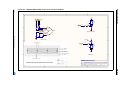
Mechanical drawing
Figure 13. STM32L-DISCOVERY
Doc ID 018789 Rev 2
27/35
Electrical schematics
UM1079
7
Figure 14. STM32L-DISCOVERY
1
2
IDD_measurement.SchDoc
U_Power
IDD_CNT_EN
IDD_WAKEUP
IDD_Measurement
A
PC13
PA0
PA4
3
ST_LINK.SCHDOC
U_ST_LINK
MCO
PA14
PA13
EXT_5V
EXT_3V
NRST
PB3
MCO
PA14
PA13
EXT_5V
EXT_3V
NRST
PB3
PC13
PA0
PA4
TCK/SWCLK
TMS/SWDIO
Doc ID 018789 Rev 2
PC13
PC12
PA4
PA0
B
P1
C
PC13
PC14
PC15
PH0
PH1
NRST
PC0
PC1
PC2
PC3
PA0
PA1
PA2
PA3
PA4
PA5
PB2
PB10
PB11
PB12
PB13
PB14
PB15
VDD
PA6
PA7
PB0
PB1
PC4
PC5
PA5
PA11
PA12
PB2
PB6
PB7
PC14
PC15
PD2
PH0
PH1
BOOT0
MCO
NRST
U_LCD_GH08172
LCD_GH08172.SchDoc
PA14
PA13
PC13
PC12
PA4
PA8
PA9
PA10
PB9
PA0
PA1
PA2
PA3
PB3
PB4
PB5
PB10
PB11
PB12
PB13
PB14
PB15
PB8
PA15
PC0
PC1
PC2
PC3
PC6
PC7
PC8
PC9
PC10
PC11
PA6
PA7
PB0
PB1
PC4
PC5
PA5
PA11
PA12
PB2
PB6
PB7
PC14
PC15
PD2
PH0
PH1
PA8
PA9
PA10
PB9
COM0
COM1
COM2
COM3
PA1
PA2
PA3
PB3
PB4
PB5
PB10
PB11
PB12
PB13
PB14
PB15
PB8
PA15
PC0
PC1
PC2
PC3
PC6
PC7
PC8
PC9
PC10
PC11
SEG0
SEG1
SEG2
SEG7
SEG8
SEG9
SEG10
SEG11
SEG12
SEG13
SEG14
SEG15
SEG16
SEG17
SEG18
SEG19
SEG20
SEG21
SEG24
SEG25
SEG26
SEG27
SEG28
SEG29
PA8
PA9
PA10
PB9
B
PA1
PA2
PA3
PB3
PB4
PB5
PB10
PB11
PB12
PB13
PB14
PB15
PB8
PA15
PC0
PC1
PC2
PC3
PC6
PC7
PC8
PC9
PC10
PC11
P2
EXT_5V
PB9
PB8
BOOT0
PB7
PB6
PB5
PB4
PB3
PD2
PC12
PC11
PC10
PA15
PA14
PA13
PA12
PA11
PA10
PA9
PA8
PC9
PC8
PC7
PC6
BOOT0
MCO
NRST
U_SLIDER_PB
SLIDER_PB.SchDoc
Header 28
NRST
D
PA0
PA6
PA7
NRST
PB0
PB1
PA0
PC4
PC5
PA6
PA7
2
C
Header 28
PB0
PB1
D
STMicroelectronics
PC4
PC5
Title:
STM32L-DISCOVERY
Number:MB963
1
1
2
3
4
5
6
7
8
9
10
11
12
13
14
15
16
17
18
19
20
21
22
23
24
25
26
27
28
3
Rev: B.1(PCB.SCH)
Date: 5/5/2011
4
Sheet 1
of
6
28/35
Electrical schematics
1
2
3
4
5
6
7
8
9
10
11
12
13
14
15
16
17
18
19
20
21
22
23
24
25
26
27
28
EXT_3V
A
T_NRST
T_SWO
U_STM32L
STM32L.SchDoc
PA14
PA13
4
1
2
3
4
TCK/SWCLK
TMS/SWDIO
PA14
PA13
NRST
PB3
T_NRST
1
X1
SWIM_IN
SWIM
C8
20pF
2
8MHz
R17
100K
OSC_IN
OSC_OUT
STM_RST
B
100nF
3V
R16
4K7
R15
4K7
R101
AIN_1
100
BAT60JFILM
48
47
46
45
44
43
42
41
40
39
38
37
36
35
34
33
32
31
30
29
28
27
26
25
R13
1
2
3
4
5
6
U2
STM32F103C8T6
VDD_2
VSS_2
JTMS/SWDIO
PA12
PA11
PA10
PA9
PA8
PB15
PB14
PB13
PB12
13
14
15
16
17
18
T_JRST 19
20
SWIM_IN 21
22
SWIM
23
24
SB102
AIN_1
VBAT
PC13
PC14
PC15
OSCIN
OSCOUT
NRST
VSSA
VDDA
PA0
PA1
PA2
T_JTCK
T_JTDO
T_JTDI
T_NRST
3V
R14
SB6
SB9
SB8
22
R102
SB11
SB10
SB13
SB12
T_NRST
22
R103
T_SWO
D5
D3
STM_JTCK
SWCLK
STM_JTMS
SWDIO
Z5V1
D4
Z5V1
22
D6
B
MCO
T_JTMS
T_JTCK
3V
SB7
T_JTMS
Header 6
STM_JTMS
USB_DP
USB_DM
T_SWO
LED_STLINK
MCO
A
T_JTCK
22
CN3
Z5V1
Z5V1
Jumpers ON --> DISCOVERY Selected
Jumpers OFF --> ST-LINK Selected
R100
100
T_SWDIO_IN
3V
LD1
VDD
1
SB21
3V
R12
1K
2
3
SB22
3V
VDD
VBAT
COM
R3
R2
LED_STLINK
C
LD2
RED
CR1
CR2032 Holder
Red
2
1
100
JP2
3
100
4
R1
0
3V
C
_Green
Not Fitted
LD_BICOLOR_CMS
PWR
U5V
CN1
VCC
DD+
ID
GND
SHELL
1
2
3
4
5
0
R8
R10
R9
R7
5V
D1
1
U5V
1K5
10 USB_DM
10 USB_DP
100K
5V
BAT60JFILM
3V
U1
Wired on Solder Side
3
INH
C1
GND
1μF_X5R_0603
C2
100nF
JP3
D2
BAT60JFILM
LD3985M33R
Vin
Vout
5
BYPASS
4
EXT_5V
2
Doc ID 018789 Rev 2
C11
1
2
3
4
5
6
7
8
9
10
11
12
D7
1
2
3
4
C9
20pF
3V
R11
10K
CN2
3V
VDD_3
VSS_3
PB9
PB8
BOOT0
PB7
PB6
PB5
PB4/JNTRST
PB3/JTDO
PA15/JTDI
JTCK/SWCLK
Not Fitted
SWD
SWD
RESERVED
100K
SB101
DEFAULT
10K
Board Ident: PC13=0
Not Fitted
STM_JTCK
R4
R6
SWIM_IN
SWIM_RST
SWIM_RST_IN
10K
PA3
PA4
PA5
PA6
PA7
PB0
PB1
PB2/BOOT1
PB10
PB11
VSS_1
VDD_1
A
R5
SB100
T_SWO
Electrical schematics
29/35
Figure 15. ST-LINK/V2 (SWD only)
3V
C3
1μF_X5R_0603
C5
10nF_X7R_0603
EXT_3V
C4
100nF
3V
5075BMR-05-SM
C6
100nF
D
USB
C7
100nF
C12
100nF
C10
100nF
JP4
Title:
STM32L-DISCOVERY ST-LINK/V2 (SWD only)
Number:MB963
1
2
D
STMicroelectronics
3
Rev: B.1(PCB.SCH)
Date: 5/5/2011
Sheet 2
of
6
4
UM1079
1
2
3
UM1079
Figure 16. STM32L-DISCOVERY MCU
4
X2
MC306-G-06Q-32.768 (manufacturer JFVNY)
C16
6.8pF
A
PB0
PB1
PB2
PB3
PB4
PB5
PB6
PB7
PB8
PB9
PB10
PB11
PB12
PB13
PB14
PB15
26
27
28
55
56
57
58
59
61
62
29
30
33
34
35
36
C
C17
6.8pF
Must be close to the Crystal
PA0/WKUP1/USART2_CTS/ADC_IN0/TIM2_CH1_ETR/COMP1_INP
PC15-OSC32_OUT
PA1/USART2_RTS/ADC_IN1/TIM2_CH2/LCD_SEG0/COMP1_INP
PC14-OSC32_IN
PA2/USART2_TX/ADC_IN2/TIM2_CH3/TIM9_CH1/LCD_SEG1/COMP1_INP
PC13
PA3/USART2_RX/ADC_IN3/TIM2_CH4/TIM9_CH2/LCD_SEG2/COMP1_INP
PC12/USART3_CK/LCD_SEG30/LCD_SEG42/LCD_COM6
PA4/SPI1_NSS/USART2_CK/ADC_IN4/DAC_OUT1/COMP1_INP
PC11/USART3_RX/LCD_SEG29/LCD_SEG41/LCD_COM5
PA5/SPI1_SCK/ADC_IN5/DAC_OUT2/TIM2_CH1_ETR/COMP1_INP
PC10/USART3_TX/LCD_SEG28/LCD_SEG40/LCD_COM4
PA6/SPI1_MISO/ADC_IN6/TIM3_CH1/TIM1_BKIN/LCD_SEG3/TIM10_CH1/COMP1_INP
PC9/TIM3_CH4/LCD_SEG27
PA7/SPI1_MOSI/ADC_IN7/TIM3_CH2/TIM1_CH1N/LCD_SEG4/TIM11_CH1/COMP1_INP
PC8/TIM3_CH3/LCD_SEG26
PA8/USART1_CK/MCO/LCD_COM0
PC7/TIM3_CH2/LCD_SEG25
PA9/USART1_TX/LCD_COM1
PC6/TIM3_CH1/LCD_SEG24
PA10/USART1_RX/LCD_COM2
PC5/ADC_IN15/LCD_SEG23/COMP1_INP
PA11/USART1_CTS/USBDM/SPI1_MISO
PC4/ADC_IN14/LCD_SEG22/COMP1_INP
PA12/USART1_RTS/USBDP/SPI1_MOSI
PC3
PA13/SWDIO
PC2
PA14/SWCLK
PC1
PA15/TIM2_CH1_ETR/PA15/SPI1_NSS/LCD_SEG17
PC0
PB0/ADC_IN8/TIM3_CH3/LCD_SEG5/COMP1_INP/VREF_OUT
PB1/ADC_IN9/TIM3_CH4/LCD_SEG6/COMP1_INP/VREF_OUT
PB2/BOOT1
PD2/TIM3_ETR/LCD_SEG31/LCD_SEG43/LCD_COM7
PB3/TIM2_CH2/PB3/TRACESWOSPI1_SCK/COMP2_INM/LCD_SEG7
PB4/TIM3_CH1/PB4/SPI1_MISO/COMP2_INP/LCD_SEG8
PB5/I2C1_SMBAl/TIM3_CH2/SPI1_MOSI/COMP2_INP/LCD_SEG9
PB6/I2C1_SCL/TIM4_CH1/USART1_TX
PB7/I2C1_SDA/TIM4_CH2/USART1_RX/PVD_IN
PH0-OSC_IN
PB8/TIM4_CH3/I2C1_SCL/LCD_SEG16/TIM10_CH1
PH1-OSC_OUT
PB9/TIM4_CH4/I2C1_SDA/LCD_COM3/TIM11_CH1
PB10/I2C2_SCL/USART3_TX/TIM2_CH3/LCD_SEG10
NRST
PB11/I2C2_SDA/USART3_RX/TIM2_CH4/LCD_SEG11
PB12/SPI2_NSS/I2C2_SMBA/USART3_CK/LCD_SEG12/ADC_IN18/COMP1_INP/TIM10_CH1
PB13/SPI2_SCK/USART3_CTS/LCD_SEG13/ADC_IN19/COMP1_INP/TIM9_CH1
PB14/SPI2_MISO/USART3_RTS/LCD_SEG14/ADC_IN20/COMP1_INP/TIM9_CH2
PB15/SPI2_MOSI/TIM1_CH3N/LCD_SEG15/ADC_IN21/COMP1_INP/TIM11_CH1/RTC_50_60Hz
BOOT0
4
3
2
53
52
51
40
39
38
37
25
24
11
10
9
8
PC13
PC12
PC11
PC10
PC9
PC8
PC7
PC6
PC5
PC4
PC3
PC2
PC1
PC0
54
PD2
PC15
PC14
SB16
LD3
R39
PB7
330
Green
LD4
R40
PB6
660
Blue
B
Not Fitted
PD2
5
6
PH0-OSC_IN
PH1-OSC_OUT
7
NRST
C21
20pF
R30
220
C22
20pF
PH1
SB20
R26
60
X3
8MHz
NRST
SB18
510
BOOT0
PH0
MCO
MCO
SB17
C
STM32L152RBT6
R27
10K
BOOT0
SB3
Must be close to the Crystal
BOOT0
U8B
fcm1608-0603
BOOT1
VDD
R32
10K
PB2
13
C26
1uF
C24
100nF
L1
32
48
64
19
VDD_MCU
1
R31
510
C25
100nF
C18
100nF
C23
100nF
R29
0
VDD
VDDA
VSSA
VDD_1
VDD_2
VDD_3
VDD_4
VSS_1
VSS_2
VSS_3
VSS_4
12
31
47
63
18
VLCD
STM32L152RBT6
C20
100nF
C19
1uF
D
STMicroelectronics
SB19
Title:
STM32L-DISCOVERY MCU
Number:MB963
1
2
3
Rev: B.1(PCB.SCH)
Date: 5/5/2011
4
Sheet 3
of
6
30/35
Electrical schematics
D
A
PC15
PC14
SB15
PC13
PC12
PC11
PC10
PC9
PC8
PC7
PC6
PC5
PC4
PC3
PC2
PC1
PC0
2
Doc ID 018789 Rev 2
PB0
PB1
PB2
PB3
PB4
PB5
PB6
PB7
PB8
PB9
PB10
PB11
PB12
PB13
PB14
PB15
14
15
16
17
20
21
22
23
41
42
43
44
45
46
49
50
1
1
B
PA0
PA1
PA2
PA3
PA4
PA5
PA6
PA7
PA8
PA9
PA10
PA11
PA12
PA13
PA14
PA15
2
4
R28
0
U8A
PA0
PA1
PA2
PA3
PA4
PA5
PA6
PA7
PA8
PA9
PA10
PA11
PA12
PA13
PA14
PA15
3
1
2
3
4
A
A
LCD
PC3
PC2
PC6
PC1
PC7
PC0
PC8
PB8
PC9
PA15
PC10
PA8
16
17
18
19
20
21
22
23
24
25
26
15
B
COM2
COM1
U4
GH08172T
14
COM0
SEG12
SEG11
COM3
13
12
SEG13
SEG10
11
SEG14
SEG9
10
SEG15
SEG8
9
SEG16
SEG7
8
SEG17
SEG6
7
SEG18
SEG5
6
SEG19
SEG4
5
SEG20
SEG3
4
SEG21
SEG2
3
SEG23
SEG22
SEG1
SEG0
1
Doc ID 018789 Rev 2
2
B
27
PA9
28
PC11
PA1
PA10
PA2
C
PB9
PA3
PB15
PB3
C
PB14
PB4
PB13
PB5
PB12
PB10
PB11
D
D
STMicroelectronics
Title:
STM32L-DISCOVERY LCD
Number:MB963
1
Electrical schematics
31/35
Figure 17. STM32L-DISCOVERY LCD
2
3
Rev: B.1(PCB.SCH)
Date: 5/5/2011
Sheet 4
of
6
4
UM1079
1
2
3
UM1079
Figure 18. STM32L-DISCOVERY IDD measurement
4
A
A
IDD Measure
VDD_MCU
1
2
on
3
1
off
JP1
5
4
R22
2(1%)
1K(1%)
3
C
VDD
S1
G1
S2
G2
PA0
SB1
D1
D1
D2
D2
8
7
6
5
C13
1uF
VDD
PA4
SB2
0
B
VDD
C14
100nF
U3
IDD_WAKEUP
U20
5
IDD_Measurement
R19
10K
U7
74LX1G04CTR
2
Doc ID 018789 Rev 2
5
VDD
1
2
3
4
R18
2
74H1G66STR
4
VDD
R21
2
B
U5
U6
MAX9938FEUK+
3
1
I/O
O/I
4
C
3
GND VCC
R20
47K
1
2
3
4
5
6
7
8
Q12 VCC
Q13
Q10
Q14
Q8
Q6
Q9
Q5
CLR
Q7
CI
Q4
CO
GND
CO
M74HC4060TTR
STS4DPF20L
16
15
14
13
12
11
10
9
VDD
R25
10K
IDD_CNT_EN
PC13
SB14
C15
1nF
R23
15K
R24
30K
C
Oscillator frequency 30KHz
D
STMicroelectronics
Title:
STM32L-DISCOVERY IDD_Measurement
Number:MB963
1
2
3
Rev: B.1(PCB.SCH)
Date: 5/5/2011
4
Sheet 5
of
6
32/35
Electrical schematics
D
1
2
3
4
VDD
PA0
PA6
PA7
PB0
PC4
PA6
B
R38
10K
PC4
GRP 2
GRP 9
GRP 3
USER & WAKE-UP Button
PC5
PB1
B
PB1
C29
47nF
VDD
Not Fitted
SLIDER 3 Positions
R37
100K
NRST
NRST
SB5
C31
C
100nF
3
2
Doc ID 018789 Rev 2
C28
47nF
330
PB0
PA7
PC5
C27
47nF
SB4
4
1
R34
10K
R33
10K
R36
PA0
3
2
100nF
R35
10K
A
SW-PUSH-CMS
B1
3
C30
SLD_3
1
2
SLD_2
SLD_1
4
1
Slider 3 pos
A
SW-PUSH-CMS
B2
3
2
1
S1
Electrical schematics
33/35
Figure 19. STM32L-DISCOVERY linear touch sensor/touchkeys
C
RESET Button
D
D
STMicroelectronics
Title:
STM32L-DISCOVERY Linear Sensor and Push Button
Number:MB963
1
2
3
Rev: B.1(PCB.SCH)
Date: 5/5/2011
Sheet 6
of
6
4
UM1079
Revision history
8
UM1079
Revision history
Table 8.
Document revision history
Date
34/35
Revision
Changes
10-May-2011
1
Initial release.
24-June-2011
2
Added Chapter 6: Mechanical drawing.
Modified Chapter 4.3: Power supply and power selection.
Doc ID 018789 Rev 2
UM1079
Please Read Carefully:
Information in this document is provided solely in connection with ST products. STMicroelectronics NV and its subsidiaries (“ST”) reserve the
right to make changes, corrections, modifications or improvements, to this document, and the products and services described herein at any
time, without notice.
All ST products are sold pursuant to ST’s terms and conditions of sale.
Purchasers are solely responsible for the choice, selection and use of the ST products and services described herein, and ST assumes no
liability whatsoever relating to the choice, selection or use of the ST products and services described herein.
No license, express or implied, by estoppel or otherwise, to any intellectual property rights is granted under this document. If any part of this
document refers to any third party products or services it shall not be deemed a license grant by ST for the use of such third party products
or services, or any intellectual property contained therein or considered as a warranty covering the use in any manner whatsoever of such
third party products or services or any intellectual property contained therein.
UNLESS OTHERWISE SET FORTH IN ST’S TERMS AND CONDITIONS OF SALE ST DISCLAIMS ANY EXPRESS OR IMPLIED
WARRANTY WITH RESPECT TO THE USE AND/OR SALE OF ST PRODUCTS INCLUDING WITHOUT LIMITATION IMPLIED
WARRANTIES OF MERCHANTABILITY, FITNESS FOR A PARTICULAR PURPOSE (AND THEIR EQUIVALENTS UNDER THE LAWS
OF ANY JURISDICTION), OR INFRINGEMENT OF ANY PATENT, COPYRIGHT OR OTHER INTELLECTUAL PROPERTY RIGHT.
UNLESS EXPRESSLY APPROVED IN WRITING BY AN AUTHORIZED ST REPRESENTATIVE, ST PRODUCTS ARE NOT
RECOMMENDED, AUTHORIZED OR WARRANTED FOR USE IN MILITARY, AIR CRAFT, SPACE, LIFE SAVING, OR LIFE SUSTAINING
APPLICATIONS, NOR IN PRODUCTS OR SYSTEMS WHERE FAILURE OR MALFUNCTION MAY RESULT IN PERSONAL INJURY,
DEATH, OR SEVERE PROPERTY OR ENVIRONMENTAL DAMAGE. ST PRODUCTS WHICH ARE NOT SPECIFIED AS "AUTOMOTIVE
GRADE" MAY ONLY BE USED IN AUTOMOTIVE APPLICATIONS AT USER’S OWN RISK.
Resale of ST products with provisions different from the statements and/or technical features set forth in this document shall immediately void
any warranty granted by ST for the ST product or service described herein and shall not create or extend in any manner whatsoever, any
liability of ST.
ST and the ST logo are trademarks or registered trademarks of ST in various countries.
Information in this document supersedes and replaces all information previously supplied.
The ST logo is a registered trademark of STMicroelectronics. All other names are the property of their respective owners.
© 2011 STMicroelectronics - All rights reserved
STMicroelectronics group of companies
Australia - Belgium - Brazil - Canada - China - Czech Republic - Finland - France - Germany - Hong Kong - India - Israel - Italy - Japan Malaysia - Malta - Morocco - Philippines - Singapore - Spain - Sweden - Switzerland - United Kingdom - United States of America
www.st.com
Doc ID 018789 Rev 2
35/35