1
EX94664 User’s manual
EX94664 User’s manual
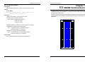
EX-94664
64 channel Digital
Input and Output
Copy Right Notice
The information in this manual is subject to change without prior notice in order t o
improve reliability, design and function and DOSed not represent a commitment on
the part of the manufacturer. No part of this manual may be reproduced, copied, or
transmitted in any form without the prior written permission of manufacturer.
Acknowledgment
Products mentioned in this manual are mentioned for identification purpose only.
Products manes appearing in this manual may or may not be registered trademarks
or copyright of their respective companies
Printed Sep. 2002 Rev 1.0
1
2
EX94664 User’s manual
Table of Contents
Chapter 1 Introduction ..................................................................................... 5
1.1
1.2
1.3
1.4
1.5
1.6
Introduction ............................................................................................... 6
Features.................................................................................................... 6
Applications............................................................................................... 6
Specifications ............................................................................................ 7
Software Supporting.................................................................................. 8
Programming Library................................................................................. 8
Chapter 2 Installation ....................................................................................... 9
2.1
2.2
2.3
2.4
2.5
2.6
2.7
What You Have ......................................................................................... 10
Unpacking ................................................................................................. 10
Hardware Installation Outline .................................................................... 10
PCB Layout............................................................................................... 11
Installation Procedures.............................................................................. 12
Device Installation for Windows Systems.................................................. 12
Connector Pin Assignment of EX-94664 ................................................... 13
Chapter 3 Registers Format............................................................................. 15
3.1
3.2
3.3
3.4
3.4.1
3.4.2
3.4.3
3.5
PCI PnP Registers .................................................................................... 16
Digital Input/Output Register Address Map ............................................... 17
PCI controller register address map.......................................................... 17
Interrupt and I/O direction control registers ............................................... 18
Digital I/O data register ............................................................................. 19
Interrupt status registers ........................................................................... 19
Interrupt mode control register .................................................................. 21
Timer/Counter registers ............................................................................ 19
EX94664 User’s manual
6.3
6.4
6.5
6.6
6.7
6.8
6.9
6.10
6.11
6.12
6.13
6.14
6.15
6.16
6.17
6.18
6.19
6.20
6.21
6.22
Chapter 7 EX-98068 Terminal board ...............................................................56
Chapter 4 Jumper setting ................................................................................ 23
4.1
4.2
Card number setting ................................................................................. 24
Input power-on state setting ...................................................................... 25
Chapter 5 Operation Theorem ......................................................................... 27
5.1
5.2
5.3
5.4
5.5
5.6
Digital Input Channels ............................................................................... 28
Digital Output Channels ............................................................................ 28
Input Initial state........................................................................................ 29
Edge Change Detection ............................................................................ 30
Digital debounce ....................................................................................... 31
Timer/Counter operation ........................................................................... 32
Chapter 6 Libraries........................................................................................... 33
6.1
6.2
Libraries Installation .................................................................................. 34
How to use the Functions in PCIDAQ.DLL................................................ 34
3
Summary of function calls..........................................................................35
W_4664_Open...........................................................................................36
W_4664_Version .......................................................................................37
W_4664_GetBusSlot .................................................................................37
W_4664_Close ..........................................................................................39
W_4664_Set_DIOMode.............................................................................40
W_4664_Read_Di .....................................................................................41
W_4664_Read_Do ....................................................................................42
W_4664_Write_Do.....................................................................................43
W_4664_Set_Do_Bit .................................................................................44
W_4664_Reset_Do_Bit .............................................................................45
W_4664_Enable_Debounce ......................................................................46
W_4664_Set_DebounceTime ....................................................................47
W_4664_Write_Counter ............................................................................48
W_4664_Read_Counter ............................................................................49
W_4664_Stop_Counter .............................................................................50
W_4664_IntEnable ....................................................................................51
W_4664_IntDisable ...................................................................................53
W_4664_Clear_IntStatus ...........................................................................54
D_4664_Read_IntStatus............................................................................55
4
EX94664 User’s manual
Chapter 1
EX94664 User’s manual
1.1
Introduction
The EX-94664 is 64-CH high-density digital input and/or output product. This I/O
card fully implements the PCI local bus specification Rev 2.1. All bus relative
configurations, such as base memory and interrupt assignment, are automatically
controlled by BIOS software.
Introduction
1.2
Features
The EX-94664 digital I/O card provide the following advanced features:
64 digital Input or output channels
Output status read back
High output driving capability, 25mA sink current on each output
External interrupt signal on DI channels (16 channels)
64-pin SCSI –1 connector (pin compatible to EX-98068) (see page 56)
1.3
Applications
Laboratory and Industrial automation
Watchdog timer
Frequency counter and generator
Low level pulse generator
Parallel data transfer
Driving indicator LEDs
5
6
EX94664 User’s manual
1.4
EX94664 User’s manual
1.5
Specifications
Numbers of I/O channel: 64 digital I/O lines
Program mode: Eight ports, each port can be programmed to input or output
Input Signal
Logic high voltage: 2.0 to 5.25 V
1.6
Logic low voltage: 0.0 to 0.80 V
Software Supporting
TOPS CCC provides versatile software drivers and packages for users’ different
approach to built-up a system. We not only provide programming library such as DLL
for many Windows systems, but also provide drivers for many software package
such as LabVIEW™ ,Intouch™ and so on. All the software options are included in
the provided CD.
Optical Isolated Input Channel
Programming Library
The provided CD includes the function libraries for many different operating systems,
including:
High level input current: 0.1 uA
Low level input current: -0.8 mA
DOS Library: Borland C/C++ and Microsoft C++, the functions descriptions
are included in this user’s guide.
Output Signal
Logic low voltage: 0.4 V maximum
Windows 98/2000/NT/Me/XP DLL: For VB, VC++, BC5, the
functionsDescriptions are included in this user’s guide.
High level output current: 15 mA maximum (source)
Windows 98/2000/NT/Me/XP ActiveX: For Windows’s applications
Low level output current: 24 mA maximum (sink)
LabVIEW ® Driver: Contains the VIs, which are used to interface with NI’s
LabVIEW ® software package. Supporting Windows 95/98/NT/2000. The
LabVIEW ® drivers are free shipped with the board.
Logic high voltage: 2.4 V minimum.
Driving capability: 15 LS TTL
Interrupt Sources
InTouch Driver: Contains the InTouch driver which support the Windows
98/2000/NT/XP. The The InTouch ® drivers are free shipped with the board.
Channel 0 to channel 15 of digital input
General Specifications
Connector: 68-pin SCSI-1connector
Operating temperature: 0°C ~ 60°C
Storage temperature: -20°C ~ 80°C
Humidity: 5 ~ 95%, non-condensing
Power Consumption: +5V 530 mA typical
Dimension: 165mm(W) x110m (H)
7
8
EX94664 User’s manual
EX94664 User’s manual
This chapter describes how to install the EX-94664 card. Please follow the follow
steps to install the EX-94664 card.
Chapter 2
Installation
2.1
What You Have
In addition to this User's Manual, the package includes the following items:
EX-94664 board
Driver/utilities CD
This user’s manual
If any of these items is missing or damaged, contact the dealer from whom you
purchased the product. Save the shipping materials and carton in case you want to
ship or store the product in the future
2.2
Unpacking
Your EX-94664 card contains sensitive electronic components that can be easily
damaged by static electricity. The operator should be wearing an anti-static
wristband, grounded at the same point as the anti-static mat. Inspect the card
module carton for obvious damage. Shipping and handling may cause damage to
your module. Be sure there are no shipping and handing damages on the module
before processing.
After opening the card module carton, extract the system module and place it only on
a grounded anti-static surface component side up. Again inspect the module for
damage. Press down on all the socketed IC's to make sure that they are properly
seated. Do this only with the module place on a firm flat surface.
2.3
Hardware Installation Outline
PCI configuration
The PCI cards are equipped with plug and play PCI controller, it can request
base addresses and interrupt according to PCI standard. The system BIOS
will install the system resource based on the PCI cards’ configuration registers
and system parameters (which are set by system BIOS). Interrupt assignment
and memory usage (I/O port locations) of the PCI cards can be assigned by
system BIOS only. These system resource assignments are done on a
board-by-board basis. It is not suggested to assign the system resource by
any other methods.
PCI slot selection
The PCI card can be inserted to any PCI slot without any configuration for
system resource.
9
10
EX94664 User’s manual
2.4
EX94664 User’s manual
2.5
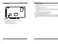
PCB Layout
Installation Procedures
1. Turn off your computer.
2. Turn off all accessories (printer, modem, monitor, etc.) connected to your
computer.
165 mm
1
3. Remove the cover from your computer.
J P1~J P3
8254
1
4. Setup jumpers on the card.
2
5. Before handling the PCI cards, discharge any static buildup on your body by
touching the metal case of the computer. Hold the edge and do not touch the
components.
J P4
102 mm
CN1
7. Secure the card in place at the rear panel of the system.
2.6
PCI Bus
Controller
Device Installation for Windows Systems
Once Windows 95/98/2000 has started, the Plug and Play function of Windows
system will find the new EXPERT cards. If this is the first time to install EXPERT
cards in your Windows system, you will be informed to input the device information
source.
CN2
CPLD
6. Position the board into the PCI slot you selected.
EX-94664
Where
JP1 ~ JP3: Digital input power initial state setting jumpers
CN1: Digital input/output connector
CN2: Testing only, no used for user
JP4: Timer /counter input/output connector
11
12
EX94664 User’s manual
2.7
EX94664 User’s manual
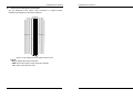
Connector Pin Assignment of EX-94664
The pin assignment of the 68-pins SCSI-II connector is a signal connector,
EX94264’s pin assignment is as shown in Figure 2.7
+5V (68)
+5V (67)
DIO_63 (66)
DIO_62 (65)
DIO_61 (64)
DIO_60 (63)
DIO_59 (62)
DIO_58 (61)
DIO_57 (60)
DIO_56 (59)
DIO_55 (58)
DIO_54 (57)
DIO_53 (56)
DIO_52 (55)
DIO_51 (54)
DIO_50 (53)
DIO_49 (52)
DIO_48 (51)
DIO_47 (50)
DIO_46 (49)
DIO_45 (48)
DIO_44 (47)
DIO_43 (46)
DIO_42 (45)
DIO_41 (44)
DIO_40 (43)
DIO_39 (42)
DIO_38 (41)
DIO_37 (40)
DIO_36 (39)
DIO_35 (38)
DIO_34 (37)
DIO_33 (36)
DIO_32 (35)
(34) GND
(33) GND
(32) DIO_31
(31) DIO_30
(30) DIO_29
(29) DIO_28
(28) DIO_27
(27) DIO_26
(26) DIO_25
(25) DIO_24
(24) DIO_23
(23) DIO_22
(22) DIO_21
(21) DIO_20
(20) DIO_19
(19) DIO_18
(18) DIO_17
(17) DIO_16
(16) DIO_15
(15) DIO_14
(14) DIO_13
(13) DIO_12
(12) DIO_11
(11) DIO_10
(10) DIO_9
(9) DIO_8
(8) DIO_7
(7) DIO_6
(6) DIO_5
(5) DIO_4
(4) DIO_3
(3) DIO_2
(2) DIO_1
(1) DIO_0
Figure 2.7 Pin Assignment of EX-94664 connector CN1
Legend:
DIO_n: Digital input /output channel #n
GND: Ground return path of input and output channels
+5V: +5VDC output (200 mA max.)
13
14
EX94664 User’s manual
EX94664 User’s manual
This information is quite useful for the programmers who wish to handle the card by
low-level programming. However, we suggest user have to understand more about
the PCI interface then start any low-level programming. In addition, the contents of
this chapter can help users understand how to use software driver to manipulate this
card.
Chapter 3
Registers Format
3.1
PCI PnP Registers
There are two types of registers: PCI Configuration Registers (PCR) and Peripheral
Interface Bus (PIB). The PCR, which is compliant to the PCI-bus specifications, is
initialized and controlled by the plug & play (PnP) PCI BIOS..
The PCI bus controller Tiger 100/320 is provided by Tigerjet Network Inc.
(www.tjnet.com). For more detailed information of PIB, please visit Tigerjet
technology’s web site to download relative information. It is not necessary for users
to understand the details of the PIB if you use the software library. The PCI PnP
BIOS assigns the base address of the PIB. The assigned address is located at offset
14h of PIB .
The EX94264 board registers are in 32-bit width. But only lowest byte (bit0~bit7) is
used. The users can access these registers by only 32-bit I/O or 8-bit I/O instructions.
The following sections show the address map, including descriptions and their offset
addresses relative to the base address.
15
16
EX94664 User’s manual
3.2
EX94664 User’s manual
3.4
Digital Input/Output Register Address Map
3.3
Interrupt and I/O direction control registers
Address: Base + 0ECh
There are 64 digital input /output channels on EX-94664, each bit of based address
is corresponding to a signal on the digital input or output channel.
Attribute: Write only
PCI controller register address map
Value:
Each bit of this I/O address controls the direction of individually port as shown
in Table 3-1
Reset control register
The EX-94664 is in inactive state when the system power on, and should be
activated by set bit o of this register to “1” state
Address: Base + 0x00h
Port
Attribute: Write only
Value: 01
Port 0
(DIO_0~DIO_7)
Port 1
(DIO_8~DIO_15)
Port 2
(DIO_16~DIO_23)
Port 3
(DIO_24~DIO_31)
Port 4
(DIO_32~DIO_39)
Port 5
(DIO_40~DIO_47)
Port 6
(DIO_48~DIO_55)
Port 7
(DIO_56~DIO_63)
Aux port direction control register
Address: Base + 002h
Attribute: Write only
Value: 7FH
Interrupt mask control register
Address: Base + 0x05h
Attribute: Write only
Value: 80H =enable PCI INT A#
00=disable PCI INT #A
Base port+0xec
Mode
Bit 7 Bit 6 Bit 5 Bit 4 Bit 3 Bit 2 Bit 1 Bit 0
0
1
0
1
0
1
0
1
0
1
0
1
0
1
0
1
Input
Output
Input
Output
Input
Output
Input
Output
Input
Output
Input
Output
Input
Output
Input
Output
Table 3-1
Note: When the system power-on, the default mode of all ports are input mode
17
18
EX94664 User’s manual
3.4.1
EX94664 User’s manual
3.5.1
Digital I/O data register
Digital I/O channels of the EX-94664 occupy eight data read/write address. Each bit
of based address is corresponding to a signal on the digital input channel.
Interrupt status registers
There are two interrupt status registers that are used to show the interrupt channel
numbers. Interrupt status register 0 stores the interrupt status of DIO_0 ~ DIO_7
(port 0), and Interrupt status register 1 stores the interrupt status of DIO_8 ~ DIO_15
(port 1).
Address: Base + 0C0h ~ Base+0DCh
Attribute: Read/Write
Address: Base + 0E0h and Base +0E4h
Value:
Attribute: Read (Read interrupt status)
Each bit of this I/O address controls the direction of individually port as shown
in Table 3-2
Value:
Base+0E0h (status register 0)
Address
Port
Bit 7
bit 6
bit 5
bit 4
bit 3
bit 2
bit 1
bit 0
Base+0C0H
0
DIO_7 DIO_6 DIO_5 DIO_5 DIO_3 DIO_2 DIO_1 DIO_0
Base+0C4H
1
DIO_15 DIO_14 DIO_13 DIO_12 DIO_11 DIO_10 DIO_9 DIO_8
Base+0C8H
2
DIO_23 DIO_22 DIO_21 DIO_20 DIO_19 DIO_18 DIO_17 DIO_16
Base+0CCH
3
DIO_31 DIO_30 DIO_29 DIO_28 DIO_27 DIO_26 DIO_25 DIO_24
Bit #n=1 DIO_n+8 generates interrupt
Base+0D0H
4
DIO_39 DIO_38 DIO_37 DIO_36 DIO_35 DIO_34 DIO_33 DIO_32
Bit #n=0 DIO_n+8 no interrupt
Base+0D4H
5
DIO_47 DIO_46 DIO_45 DIO_44 DIO_43 DIO_42 DIO_41 DIO_40
Address: Base +0E4h
Base+0D8H
6
DIO_55 DIO_54 DIO_53 DIO_52 DIO_51 DIO_50 DIO_49 DIO_48
Attribute: Write (Clear interrupt status registers)
Base+0DCH
7
DIO_63 DIO_62 DIO_61 DIO_60 DIO_59 DIO_58 DIO_57 DIO_56
Value: any value
Bit #n=1 DIO_n generates interrupt
Bit #n=0 DIO_n no interrupt
Base+0E4h (status register 1)
Table 3-2
3.5
Timer/Counter registers
The 8254 chip occupies 4 I/O addresses in the EX-94664. Please refer to NEC's or
Intel's data sheet for the full description of the 8254 operation.
Address: Base +0F0h ~ Base +0FCh
Attribute: Write/read
Value:
Base +0F0h Bit 7~Bit 0: Counter 0 Register
Base +0F4h Bit 7~Bit 0: Counter 1 Register
Base +0F8h Bit 7~Bit 0: Counter 2 Register
Base +0FCh Bit 7~Bit 0: Control Register
19
20
EX94664 User’s manual
3.5.2
EX94664 User’s manual
Interrupt mode control register
There are sixteen channels can generate interrupt when the input signal level
changed (falling or rising). Users can set relative bit(s) of this I/O address to define
which level change desired to generate interrupt
Address: Base +0E0h
Attribute: Write
Value:
Port
7
6
5
Port 0
(DIO_0~DIO_7)
Port 1
(DIO_8~DIO_15)
Timer #2
Debounce
Bit number
4
3
2
0
0
0
0
0
0
0
1
1
x
0
1
1
0
1
1
Interrupt mode
0
x No Interrupt
0 Rising edge
1 Falling edge
No Interrupt
Rising edge
Falling edge
1
x
x
x
x Timer Interrupt
0
0
x
x
x
x
0
1
x
x
x
x
1
0
x
x
x
x
1
1
x
x
x
x
x No debounce
Enable port 0
xx debounce
function
Enable port 1
x debounce
function
Enable port 0/1
x debounce
function
Note: “ x “ means don’t care
21
22
EX94664 User’s manual
Chapter 4
EX94664 User’s manual
4.1
Card number setting
Maximum three EX-94664 cards can be installed in system simultaneously with each
has a unique card number.
Jumper setting
A jumper called “JP5” (see page 11 on the card is used to set the card number starts
from 1 to 4
JP5
23
24
Card number
3
2
1
1
(default setting)
3
2
1
2
3
2
1
3
EX94664 User’s manual
4.2
EX94664 User’s manual
Input power-on state setting
Each channel of EX-94664 are all reset to input mode when the system
power-on. The power-on initial state of channels is something importance for
user’s application.
There are three jumpers called JP1, JP2, and JP3 are used to set the
power –on initial state of each port (port 0 ~ port 7)
Pin #n+1 of JP2 controls the initial state of port #n (n=0~7)
Power-on Initial state
High
Low
Port number
Port 0
(DIO_0~DIO_7)
Port 1
(DIO_8~DIO_15)
Port 2
(DIO_16~DIO_23)
Port 3
(DIO_24~DIO_31)
Port 4
(DIO_32~DIO_39)
Port 5
(DIO_40~DIO_47)
Port 6
(DIO_48~DIO_55)
Port 7
(DIO_560~DIO_63)
1
8
1
8
JP1
JP2
JP3
1
JP1
JP2
JP3
1
8
8
JP1
JP2
JP3
JP1
JP2
JP3
1
1
8
8
JP1
JP2
JP3
JP1
JP2
JP3
1
1
8
8
JP1
JP2
JP3
JP1
JP2
JP3
1
8
1
8
JP1
JP2
JP3
1
JP1
JP2
JP3
1
8
8
JP1
JP2
JP3
JP1
JP2
JP3
1
1
8
8
JP1
JP2
JP3
JP1
JP2
JP3
1
1
8
JP1
JP2
JP3
8
JP1
JP2
JP3
25
26
EX94664 User’s manual
Chapter 5
EX94664 User’s manual
5.1
Digital Input Channels
Each digital input is a TTL structure. The input voltage range form 0V to 5V and input
pull-up resister is 10K ohms. The connection between outside signal and EX-94664
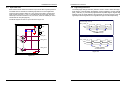
digital inputs is shown in Fig 5.1.
Operation Theorem
+5V
10K
Digital voltage input
DIO_n (0~63)
+
V 0 ~5V
-
GND
In/Out control
+5V
10K
Digital dry input
DIO_n (0~63)
GND
In/Out control
Figure 4-1 digital inputs of EX-94232
5.2
Digital Output Channels
On EX-94664, each port can be programmed to output port by setting Base + 0ECh
register (See page 18). Each output channel is TTL compatible with sink current
25mA max. The connection between outside loading and EX-94664 outputs is
shown in Fig 4.2
+5V
10K
Digital output
DIO_n (0~63)
Loading
In/Out control
GND
Figure 4-2 digital output of EX-94232
27
28
EX94664 User’s manual
5.3
EX94664 User’s manual
5.4
Input Initial state
Each channel of EX-94664 are all reset to input mode when system power-on.
The initial state of channels is something importance for user’s application.
Edge Change Detection
The ECD (Edge Change Detection) detection circuit is used to detect the edge of
level change. In the EX-94664, the detection circuit is applied to 16 input channels
(DIO_0 and DIO_15). If channel is programmed to be positive edge or negative edge
interrupt mode, the ECD detection circuit generate an interrupt request, when the
signal inputs are changed from low to high level or high to low level respectively
There are three jumpers called JP1, JP2, and JP3 are used to set the initial
state of each port (port 0 ~ port 7). The initial state of port is high, when the
relative pin of the JP2 shorted to JP1, and is low, when the relative pin of the
JP2 shorted to JP3 (see page 25)
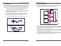
The block diagram of each I/O port is shown in Figure 5-3
Positive Edge Interrupt
Port n (n =0 ~ 7)
DIO_0~DIO_15
Initial State
+5V
J P1
ECD
High
INT
J P2
J P3
Low
Generate Interrupt
D0
DIO_m
Negative Edge Interrupt
D0
DIO_m+1
DIO_0~DIO_15
ECD
INT
D7
DIO_m+7
Generate Interrupt
Figure 5-4
Figure 5-3
29
30
5.5
EX94664 User’s manual
5.6
Digital debounce
Each digital input channel of port 0 and port 1 (DIO_0~DIO_15) has a programmable
digital debounce for eliminating unexpected signals and noise from the card circuitry.
The user can set different digital debouncing parameters for each input channel in
different applications. The following is a functional description of the digital debounce.
1.
When a digital debounce is enabled, the EX-94664 will sample the
signals at the enabled input channel at a 10 ms sampling rate.
2.
When a high or low signal is present at a digital input channel whose
digital debounce function is enabled, the signal will be filtered out as noise
unless it lasts for an effective period.
3.
Timer/Counter operation
One 8254 programmable timer/counter chip is installed in the EX-94664. There are
three counters in one 8254 chip and 6 possible operation modes for each counter.
The block diagram of the timer /counter system is shown in Figure 4-6
2M OSC
Debounce_TimeBase
CLK #0
Counter #0
The effective period is determined by multiplying the sampling rate
(0.002 ms) by the sampling number (1 ~ 65535) chosen by the user, i.e.
1
OUT #0
2
CLK #1
Effective debounce timer period = time number x 0.002 ms.
4.
GATE #0
See Sec 6.15 (page 47) to more detail using of debounce function
Counter #1
GATE #1
3
OUT #1
4
Connector JP4
EX94664 User’s manual
CLK #2
Disable Debounce
7
DIO_0~DIO_15
Counter #2
GATE #2
5
OUT #2
6
8
Read IN
Noise
Time_Out
Signal
Figure 4-6
Noise
Enable Debounce
Timer #1 and timer #2 of the 8254 chip are cascaded as a 32-bits programmable
timer. In the software library, timer #1 and #2 are always set as mode 2 (rate
generator). Counter #0 is used as time base of input debounce counter, that is, there
is an interrupt on the terminal count of 8254 mode 0.
DIO_0~DIO_15
Read IN
The base frequency of input clock for the cascaded timer is 2MHz. The output is sent
to be the timer interrupt. To set the maximum and minimum frequency of the timer,
please refer to the timer functions in next chapter
Debounce period=0.002 msec x n
The timer #0 of 8254 is used to be a time base of debounce counter. The output of
timer #0 is feed into the digital debounce counter. Changing this timer’s value can
change the debounce time interval to filter varies input noise
Figure 5-5
31
32
EX94664 User’s manual
EX94664 User’s manual
This chapter describes the software library for operating this card. Only the functions
in DOS library and Windows 95 DLL are described. Please refer to the PCIDAQ
function reference manual, which included in TOPS CCC CD for the descriptions of
the Windows 98/NT/2000 DLL functions.
Chapter 6
Libraries
6.1
Libraries Installation
The device drivers and DLL functions of Windows 98/NT/2000 are included in the
PCIDAQ. The TOPS CCC CD also includes the detail examples and readme files
6.2
How to use the Functions in PCIDAQ.DLL
VC++6.0:
1.
Add file '../Include/PCIDAQ.H' in your project
2.
In link page of menu project| setting, add '../LIB/PCIDAQ.LIB' in the
blank of Objects/Library Modules
3.
Add this sentence "#include '../Include/PCIDAQ.H' " to the head of your
main file.
Visual BASIC:
1.
Add file '../Include/Declare.bas' in your project.
Delphi:
1.
2.
Add file '../Include/Declare.pas' in your project
Add this sentence "uses Declare;" in the head of your unit.pas
C++Builder:
1.
2.
Add file '../Include/PCIDAQ.H' and '../Lib/PCIDAQ_CB.lib' to your project
Add this sentence "#include '../Include/PCIDAQ.H' " to head of your
main file.
Note: For more information, please refer to program in directory '../Example/'
33
34
EX94664 User’s manual
6.3
EX94664 User’s manual
6.4
Summary of function calls
W_4664_Open
Description:
Function
Description
Because the EX-94664 is PCI bus architecture and meets the plug and play
design, the IRQ and base_address (pass-through address) are assigned by
system BIOS directly. EX-94664 cards have to be initialized by this function
before calling other functions.
Page
W_4664_Open
Initial EX-94664 card before using
35
W_4664_Version
Get version number of PCIDAQ.DLL
37
W_4664_GetBusSlot
Get PCI bus and slot number occupied by
EX-94664
37
W_4664_Close
Close EX-94664 card before terminating
program
39
W_4664_Set_DIOMode
Set port direction (input or output)
40
Function W_4664_Open (ByRef ExistedCards As Long) As Long
W_4664_Read_Di
Read digital input port data (8-bit)
41
Delphi
W_4664_Read_Do
Read back current value of digital output
port
42
W_4664_Write_Do
Write data (8-bit) to digital output port
43
CardNo: card number (1,2,3,4) (for DOS only)
W_4664_Set_Do_Bit
Set a bit of port to high
44
existCards: The number of installed EX-98354 cards. (for Windows only)
W_4664_Reset_Do_Bit
Reset a bit of port to low
45
This returned value shows how many EX-98354 cards are installed in your
system.
Syntax:
W_4664_Enable_Debounce Enable input debounce function
46
W_4664_Set_DebounceTime Set debounce time period
47
W_4664_Write_Counter
48
Write command and value to timer/counter
W_4664_Read_Counter
Read counter value or control value
49
W_4664_Stop_Counter
Stop timer/counter
50
W_4664_Clear_IntStatus
Clear interrupt status
48
W_4664_IntEnable
Enable digital input change interrupt
51
W_4664_IntDisable
Disable digital input interrupt
53
W_4664_Clear_IntStatus
Clear interrupt status register
54
W_4664_Read_IntStatus
Read interrupt status register
55
35
C/C++ (DOS)
WORD D_4664_Open (WORD cardNo);
C/C++ (Windows)
WORD W_4664_Open (WORD *ExistedCards);
Visual BASIC (Windows)
Function W_4664_Open (var ExistedCards:Integer):Integer;
Argument:
Return Code:
Error code (Please refer to PCIDAQ.H or DOSDAQ.H)
36
EX94664 User’s manual
6.5
EX94664 User’s manual
6.6
W_4664_Version
Description:
W_4664_GetBusSlot
Description:
PCIDAQ.DLL driver drives the EX-94664. This function returns the version of
PCIDAQ.DLL driver
Get the PCI bus and slot number of the card
Syntax:
Syntax:
C/C++ (DOS)
C/C++ (DOS)
WORD D_4664_GetBusSlot (WORD cardNo, WORD *bus,WORD *slot);
void D_4664sion (char *version)
C/C++ (Windows)
C/C++ (Windows)
WORD W_4664_GetBusSlot (WORDcardNo, WORD *bus,WORD *slot);
Int W_4664_Version (void);
Visual BASIC (Windows)
Visual BASIC (Windows)
Function W_4664_Version () As Long
Function W_4664_GetBusSlot (ByValcardNo As Long,
ByRef bus As Long, ByRef slot As Long) As Long
Delphi
Delphi
Function W_4664_Version ():Integer;
Function W_4664_GetBusSlot (cardNo:Integer;var
bus:Integer;var slot:Integer):Integer;
Argument:
Argument:
Version: return the PCIDAQ.DLL driver version string (DOS only)
cardNo: card number to select borad (1,2,3,4),It's set by jumper on card
Return Code:
bus :return PCI bus Number
The version of PCIDAQ.DLL in integer data format (Windows only)
slot :Return PCI slot Number of the bus
Return Code:
Error code (Please refer to PCIDAQ.H or DOSDAQ.H)
37
38
EX94664 User’s manual
6.7
EX94664 User’s manual
6.8
W_4664_Close
Description:
W_4664_Set_DIOMode
Description:
The IRQ and base_address of EX-94664 ( pass-through address) are
assigned by system BIOS directly. This function should be called to release all
system resource before terminate application program
Set port0~port7 is output port or input port
Syntax:
C/C++ (DOS)
Syntax:
WORD D_4664_Set_DIOMode (WORD cardNo,BYTE DIO_Direction);
C/C++ (DOS)
C/C++ (Windows)
WORD D_4664_Close (WORD cardNo);
WORD W_4664_Set_DIOMode (WORDcardNo,BYTE DIO_Direction);
C/C++ (Windows)
Visual BASIC (Windows)
Void W_4664_Close (void);
Visual BASIC (Windows)
Function W_4664_Set_DIOMode (ByValcardNo As Long,
ByVal DIO_Direction As Byte) As Long
Function W_4664_Close ()
Delphi
Delphi
Function W_4664_Set_DIOMode (cardNo:Integer;DIO_Direction:
Integer):Integer;
Function W_4664_Close ();
Argument:
Argument:
None
cardNo: card number (1,2,3,4),It's set by jumper on card
DIO_Direction: set Port 0 to Port 7 is Input or output
Return Code:
None
Bit 0=1 port #0 input mode / =0 output mode (DIO_0~DIO_7)
Bit 1=1 port #1 input mode / =0 output mode (DIO_8~DIO_15)
Bit 2=1 port #2 input mode / =0 output mode (DIO_16~DIO_23)
Bit 3=1 port #3 input mode / =0 output mode (DIO_24~DIO_31)
Bit 4=1 port #4 input mode / =0 output mode (DIO_32~DIO_39)
Bit 5=1 port #5 input mode / =0 output mode (DIO_40~DIO_47)
Bit 6=1 port #6 input mode / =0 output mode (DIO_48~DIO_55)
Bit 7=1 port #7 input mode / =0 output mode (DIO_56~DIO_63)
Return Code:
Error code (Please refer to PCIDAQ.H or DOSDAQ.H)
39
40
EX94664 User’s manual
6.9
EX94664 User’s manual
6.10
W_4664_Read_Di
Description:
W_4664_Read_Do
Description:
This function is used to read data from digital input port. You can get 8-bit
input data from EX-94664 by calling this function.
This function is used to read current data of output port. You can read back
8-bit output data of EX-94664 by calling this function.
Syntax:
Syntax:
C/C++(DOS)
C/C++ (DOS)
WORD D_4664_Read_Di (WORD cardNo,WORD portNo,WORD *DiData);
WORD D_4664_Read_Do (WORD cardNo,WORD portNo,WORD *DoData);
C/C++ (Windows)
C/C++ (Windows)
WORD W_4664_Read_Di (WORDcardNo,WORDportNo,WORD *DiData);
WORD W_4664_Read_Do (WORDcardNo,WORDportNo,WORD *DoData);
Visual BASIC (Windows)
Visual BASIC (Windows)
Function W_4664_Read_Di(ByValcardNo As Long,
ByValportNo As Long, ByRef DiData As Long) As Long
Function W_4664_Read_Do (ByValcardNo As Long, ByValportNo
As Long, ByRef DoData As Long) As Long
Delphi
Delphi
Function W_4664_Read_Di(cardNo:Integer;portNo:Integer;
var DiData: Integer):Integer;
Function W_4664_Read_Do (cardNo:Integer;portNo:Integer;
var DoData:Integer):Integer;
Argument:
Argument:
cardNo: card number, It’s set by jumper on card
cardNo: card number (1,2,3,4) , It’s set by jumper on card
portNo : Digital Input port number (0 ~ 7)
portNo : Digital port number (0 ~7)
Didata : Return digital input data
Data:Return current output data
Return Code:
Return Code:
Error code (Please refer to PCIDAQ.H or DOSDAQ.H)
Error code (Please refer to PCIDAQ.H or DOSDAQ.H)
41
42
EX94664 User’s manual
6.11
EX94664 User’s manual
6.12
W_4664_Write_Do
Description:
W_4664_Set_Do_Bit
Description:
This function is used to write data to output port. You can send 8-bit output
data to EX-94664 by calling this function.
Set digital output channel (bit of port) to high state
Syntax:
Syntax:
C/C++ (DOS)
C/C++ (DOS)
WORD D_4664_Write_Do (WORD cardNo,WORD portNo,WORD Data);
WORD D_4664_Set_Do_Bit (WORD cardNo,WORD portNo, WORD
bitNo);
C/C++ (Windows)
C/C++ (Windows)
WORD W_4664_Write_Do (WORDcardNo,WORDportNo,WORD Data);
WORD W_4664_Set_Do_Bit (WORDcardNo,WORDportNo, WORDbitNo);
Visual BASIC (Windows)
Visual BASIC (Windows)
Function W_4664_Write_Do (ByValcardNo As Long,
ByValportNo As Long, ByVal Data As Long) As Long
Function W_4664_Set_Do_Bit (ByValcardNo As Long,
ByValportNo As Long, ByValbitNo As Long) As Long
Delphi
Delphi
Function W_4664_Write_Do (cardNo:Integer;portNo:Integer;
Data:Integer):Integer;
Function W_4664_Set_Do_Bit
(cardNo:Integer;portNo:Integer;bitNo:Integer)
:Integer;
Argument:
Argument:
cardNo: card number (1,2,3,4)
portNo : Do port number (0 ~ 7)
cardNo: card number (1,2,3,4), It's set by jumper on card
Data : Data be written to output port
portNo: digital output port number (0 ~ 7)
bitNo: bit Number (0 to 7)
Return Code:
Return Code:
Error code (Please refer to PCIDAQ.H or DOSDAQ.H)
Error code (Please refer to PCIDAQ.H or DOSDAQ.H)
43
44
EX94664 User’s manual
6.13
EX94664 User’s manual
6.14
W_4664_Reset_Do_Bit
Description:
W_4664_Enable_Debounce
Description:
Set digital output channel (bit of port) to low state
The digital input channels DIO_0 ~ DIO_15 are grouped into 2 ports (port 0
and port 1), each port can has an individually programmable digital debounce
circuit which can filter the bounce of input signals
Syntax:
C/C++ (DOS)
Syntax:
WORD D_4664_Reset_Do_Bit (WORD cardNo,WORD portNo, WORD
bitNo);
C/C++ (DOS)
C/C++ (Windows)
WORD D_4664_Enable_Debounce (WORD cardNo,WORD portNo);
C/C++ (Windows)
WORD W_4664_Reset_Do_Bit (WORDcardNo,WORDportNo,
WORDbitNo);
WORD W_4664_Enable_Debounce (WORD cardNo,BYTE portNo);
Visual BASIC (Windows)
Visual BASIC (Windows)
Function W_4664_Reset_Do_Bit (ByValcardNo As Long,
ByValportNo As Long, ByValbitNo As Long) As Long
Function W_4664_Enable_Debounce (ByVal cardNo As Long,
ByVal portNo As Long) As Long
Delphi
Delphi
Function W_4664_Reset_Do_Bit
(cardNo:Integer;portNo:Integer;bitNo:Integer):In
teger;
Function W_4664_Enable_Debounce (cardNo:Integer;
portNo:Integer):Integer;
Argument:
Argument:
cardNo: card number, It’s set by jumper on card
cardNo: card number, It's set by jumper on card
portNo :
portNo : digital output port number (0 ~ 7)
Bit 0: =1 Enable port #0 debounce function
bitNo : bit number (0 to 7)
Bit 0: =0 Disable port #0 debounce function
Return Code:
Bit 1: =1 Enable port #1 debounce function
Error code (Please refer to PCIDAQ.H or DOSDAQ.H)
Bit 1: =0 Disable port #1 debounce function
Return Code:
Error code (Please refer to PCIDAQ.H or DOSDAQ.H)
45
46
EX94664 User’s manual
6.15
EX94664 User’s manual
6.16
W_4664_Set_DebounceTime
Description:
W_4664_Write_Counter
Description:
Set the debounce time period of port #0 (DIO_0~DIO_7) and/or port
#1(DIO_8~DIO_15)
Set counter1 and counter2's work mode and initial value
Syntax:
Syntax:
C/C++ (DOS)
C/C++ (DOS)
WORD D_4664_Write_Counter (WORD cardNo, WORD cntNo, WORD
counterVal);
WORD D_4664_Set_DebounceCLK (WORD cardNo,WORD
TimeInterval);
C/C++ (Windows)
C/C++ (Windows)
WORD W_4664_Write_Counter (WORD cardNo, WORD cntNo, WORD mode,
WORD cntrVal);
WORD W_4664_Set_DebounceTime (WORD cardNo, float
TimeInterval);
Visual BASIC (Windows)
Visual BASIC (Windows)
Function W_4664_Write_Counter (ByVal cardNo As Long, ByVal
cntNo As Long,ByVal mode As Long,ByVal cntrVal as
Long) As Integer
Function W_4664_Set_DebounceTime (ByVal cardNo As Long,
ByVal TimeInterval As Single) As Long
Delphi
Delphi
Function W_4664_Set_DebounceTime (cardNo:Integer;
TimeInterval:Single):Integer;
Function W_4664_Write_Counter
(cardNo:Integer;cntNo:Integer; mode:Integer;
cntrVal:Integer):Integer;
Argument:
Argument:
cardNo: card number (1,2,3,4), It's set by jumper on card
cardNo: card number (1,2,3,4), It's set by jumper on card
TimeInterval: debounce Time period from 0.001ms to 132ms (for Windows)
and from 0000 to 65535 for (DOS)
cntNo: Counter Number(1~2)
mode: Work mode of the counter (0~5)
Return Code:
Error code (Please refer to PCIDAQ.H or DOSDAQ.H)
cntrVal: initial value of counter (0~65535)
Return Code:
Error code (Please refer to PCIDAQ.H or DOSDAQ.H)
47
48
EX94664 User’s manual
6.17
EX94664 User’s manual
6.18
W_4664_Read_Counter
Description:
W_4664_Stop_Counter
Description:
Read counter1 and counter2's work mode and initial value
Stop counter by writing work mode 5
Syntax:
Syntax:
C/C++ (DOS)
C/C++ (DOS)
WORD D_4664_Read_Counter (WORD cardNo,WORD cntNo, WORD *mode,
WORD *cntrVal);
WORD D_4664_Stop_Counter (WORD cardNo, WORD cntNo);
C/C++ (Windows)
WORD W_4664_Stop_Counter (WORD cardNo, WORD cntNo,WORD
*cntrVal);
C/C++ (Windows)
WORD W_4664_Read_Counter (WORD cardNo, WORD cntNo, WORD *mode,
WORD *cntrVal);
Visual BASIC (Windows)
Visual BASIC (Windows)
Function W_4664_Stop_Counter (ByVal cardNo As Long,
ByVal cntNo As Long,ByRef cntrVal as Long) As
Integer
Function W_4664_Read_Counter (ByVal cardNo As Long, ByVal
cntNo As Long,ByRef mode As Long,ByRef cntrVal as
Long) As Integer
Delphi
Delphi
Function W_4664_Read_Counter (cardNo:Integer;cntNo:Integer;
var mode:Integer; var cntrVal:Integer):Integer;
Function W_4664_Stop_Counter (cardNo:Integer;cntNo:Integer;
var cntrVal:Integer):Integer;
Argument:
Argument:
cardNo: card number (1,2,3,4), It’s set by jumper on card
cardNo: card number (1,2,3,4), It’s set by jumper on card
cntNo: Counter Number(1~2)
cntNo: Counter Number(1~2)
mode: returned Work mode of the counter (0~5)
mode: returned Work mode of the counter (0~5)
cntrVal: returned current value of counter (0~65535)
cntrVal: returned current value of counter (0~65535)
Return Code:
Return Code:
Error code (Please refer to PCIDAQ.H or DOSDAQ.H)
Error code (Please refer to PCIDAQ.H or DOSDAQ.H)
49
50
EX94664 User’s manual
6.19
EX94664 User’s manual
userIntRoutine: user Interrupt service routine called when interrupt occurs.
W_4664_IntEnable
for C++: void userIntRoutine(WORD CardNo,DWORD IntStatus);
Description:
for VB : Sub UserIntRutine(ByVal CardNo As Long, ByVal IntStatus As Long)
Enable Interrupt of input port 0 or input port 1
for Delphi : procedure useIntRutine(CardNo:Word;IntStatus:Word);StdCall;
Syntax:
Note:
C/C++(DOS)
WORD D_4664_IntEnable (WORD cardNo,WORD IntMode,
*UserIntServiceRoutine());
This routine will return CardNo and IntStatus to useIntRutine()
C/C++ (Windows)
IntStatus:
WORD W_4664_IntEnable (WORDcardNo,BYTE IntMode,
User_Interrupt_HANDLER userIntRoutine);
For 0≤ n ≤15
CardNo: the card number that generate interrupts
Bit n =1 indicates the DIO_n generates interrupt
Visual BASIC (Windows)
=0 indicate the DIO_n no interrupt
Function W_4664_IntEnable (ByValcardNo As Long, ByVal
IntMode As Byte, ByVal userIntRoutine As Long) As
Long
Bit 16 =1 indicate the timer interrupt
Return Code:
Error code (Please refer to PCIDAQ.H or DOSDAQ.H)
Delphi
Function W_4664_IntEnable (cardNo:Integer;IntMode:Integer;
userIntRoutine:Pointer):Integer;
Argument:
cardNo: card number, It’s set by jumper on card
IntMode: Interrupt mode of input port #0 and #1 (DIO_0~DIO_15)
Bit 0
=1 Falling edge trigger of all port 0’s channel (DIO_0~DIO_7)
=0 Rising edge trigger of all port 0’s channel (DIO_0~DIO_7)
Bit 1
=1 Enable interrupts of port 0
=0 Disable interrupts of port 0
Bit 2
=1 Falling edge trigger of all port 1’s channel (DIO_8~DIO_15)
=0 Rising edge trigger of all port 1’s channel (DIO_8~DIO_15)
Bit 3
=1 Enable interrupts of port 1
=0 Disable interrupts of port 1
Bit 4
=1 Enable Interrupt of Timer
=0 Disable Interrupt of Timer
Bit 5
~ =0 Always zero
Bit 7
51
52
EX94664 User’s manual
6.20
EX94664 User’s manual
6.21
W_4664_IntDisable
Description:
W_4664_Clear_IntStatus
Description:
Disable interrupt of channel0 of input port0 and chanel0 of input port1
Clear interrupt by writing random data to Base Port+D0h
Syntax:
Syntax:
C/C++(Dos)
C/C++ (DOS)
WORD D_4664_IntDisable (WORD cardNo);
WORD D_4664_Clear_IntStatus (WORD cardNo);
C/C++ (Windows)
C/C++ (Windows)
Void W_4664_IntDisable (WORDcardNo);
WORD W_4664_Clear_IntStatus (WORD cardNo);
Visual BASIC (Windows)
Visual BASIC (Windows)
Function W_4664_IntDisable (ByValcardNo As Long)
Function W_4664_Clear_IntStatus (ByVal cardNo As Long) As
Long
Delphi
Delphi
Function W_4664_IntDisable (cardNo:Integer);
Function W_4664_Clear_IntStatus (cardNo:Integer):Integer;
Argument:
Argument:
cardNo: card number, It’s set by jumper on card
cardNo: card number, It’s set by jumper on card
Return Code:
Return Code:
Error code (Please refer to PCIDAQ.H or DOSDAQ.H)
Error code (Please refer to PCIDAQ.H or DOSDAQ.H)
53
54
EX94664 User’s manual
6.22
EX94664 User’s manual
D_4664_Read_IntStatus
Chapter 7
EX-98068 Terminal board
Description:
Read interrupt status of port_0, port_1 and Timer (for DOS only)
Syntax:
EX-98068 digital input/output termination board features one DIN socket for easy
maintenance, wiring, and installation. It provides 68 channels that are accessed
through a SCSI-68 connector.
C/C++ (DOS)
WORD D_4664_Read_IntStatus (WORD cardNo, struct
IntStatus_4664 *IntStatus);
Each terminal pin is in serial with 0 ohms resistor to relative pin on the DIN connector.
These resistors can be changed to the desired value to meet the requirement of your
applications
Argument:
cardNo: card number, It’s set by jumper on card
IntStatus: pointer of interrupt structure
struct IntStatus_4664{ BYTE TimerFlag;
SCSI-I 68-pin connector
BYTE Port_0Flag;
1
2
3
4
5
6
7
8
9
10
11
12
13
14
15
16
17
18
19
20
21
22
23
24
25
26
27
28
29
30
31
32
33
34
BYTE Port_1Flag;
};
IntStatus.TimerFlag = TRUE/FAIL: Timer Interrupt / no Interrupt
IntStatus.Port_0Flag=Port #0 Interrupt Status
Bit n =1 indicates the DIO_n generates interrupt
=0 indicate the DIO_n no interrupt
IntStatus.Port_1Flag: Port #1Interrupt Status
Bit n =1 indicates the DIO_n+8 generates interrupt
=0 indicate the DIO_n+8 no interrupt
Return Code:
Error code (Please refer to PCIDAQ.H or DOSDAQ.H)
35
36
37
38
39
40
41
42
43
44
45
46
47
48
49
50
51
52
53
54
55
56
57
58
59
60
61
62
63
64
65
66
67
68
EX-98068 Terminal board
55
56