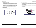
1
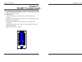
EX92026 User’s manual
EX92026 User’s manual
EX-92026
Multi-function DAS
Cards
User’s Guide
Copy Right Notice
The information in this manual is subject to change without prior notice in order t o
improve reliability, design and function and DOSed not represent a commitment on
the part of the manufacturer. No part of this manual may be reproduced, copied, or
transmitted in any form without the prior written permission of manufacturer.
Acknowledgment
Products mentioned in this manual are mentioned for identification purpose only.
Products manes appearing in this manual may or may not be registered trademarks
or copyright of their respective companies
Printed Aug. 2002 Rev 1.0
1
2
EX92026 User’s manual
EX92026 User’s manual
Table of Contents
Chapter 1 Introduction ..................................................................................... 7
1.1
1.2
1.3
1.4
1.5
Features.................................................................................................... 8
Applications............................................................................................... 8
Specifications ............................................................................................ 9
Software Supporting.................................................................................. 11
Programming Library................................................................................. 11
Chapter 2 Installation ....................................................................................... 13
2.1
2.2
2.3
2.4
What You Have ......................................................................................... 14
Unpacking ................................................................................................. 14
Hardware Installation Outline .................................................................... 14
PCB outline ............................................................................................... 15
Chapter 3 Connector Pin Assignments .......................................................... 17
3.1
3.2
Analog input/output & digital input/output (CN2) ....................................... 18
Timer/counter #0 (JP5) ............................................................................. 18
Chapter 4 Jumper Setting................................................................................ 19
4.1
4.2
4.3
4.4
Card number setting ................................................................................. 20
Analog Signal Input (A/D) Type selection.................................................. 20
Analog Input Polarity and Range selection ............................................... 21
Analog output (D/A) range selection ......................................................... 21
Chapter 5 Registers Format............................................................................. 23
5.1
5.2
5.3
5.4
5.5
5.6
5.7
5.8
5.9
5.10
5.11
5.12
5.13
5.14
5.15
PCI PnP Registers .................................................................................... 24
PCI controller register address map.......................................................... 24
Digital Input Register Address Map ........................................................... 25
Digital Output Register .............................................................................. 25
Read FIFO data register ........................................................................... 25
Read FIFO status register......................................................................... 26
A/D control register ................................................................................... 26
A/D control status register......................................................................... 27
Interrupt Control and Read back Register................................................. 27
Software Trigger Register ......................................................................... 28
Hardware Interrupt Clear Register ............................................................ 28
Clear scan register .................................................................................... 28
D/A control and data registers................................................................... 28
Timer/Counter Register............................................................................. 29
High Level Programming........................................................................... 29
6.1
6.2
6.3
6.4
6.5
6.6
6.7
Digital Input Channels................................................................................32
Isolated Digital Output Channels ...............................................................32
A/D Signal Source Control .........................................................................33
A/D Trigger Source Control........................................................................36
A/D Data Transfer Modes ..........................................................................36
Interrupt Control.........................................................................................37
Timer/Counter Operation ...........................................................................38
Chapter 7 Libraries............................................................................................39
7.1
7.2
7.3
7.4
7.5
7.6
7.7
7.8
7.9
7.10
7.11
7.12
7.13
7.14
7.15
7.16
7.17
7.18
7.19
7.20
7.21
7.22
7.23
7.24
7.25
7.26
7.27
7.28
How to use the DOSDAQH.LIB in DOS .....................................................40
How to use the PCIDAQH.DLL in Windows ...............................................40
Open EX-92026 card .................................................................................41
Get card number setting ............................................................................42
Get Version of PCIDAQ.DLL or DOSDAQ.LIB...........................................43
Close EX-92026 card before exiting ..........................................................44
Read data from digital input port ................................................................45
Get the PCI bus and slot number of the card.............................................46
Write data to digital output port ..................................................................47
Read back current value of the digital output port......................................48
Set a bit of digital output port .....................................................................49
Reset a bit of digital output port .................................................................50
Initial software trigger mode.......................................................................51
Single A/D channel acquire........................................................................52
Multiple A/D channels acquire....................................................................53
Initial interrupt trigger mode .......................................................................54
Start A/D auto scan ....................................................................................55
Get A/D scanning data ...............................................................................56
Stop auto scan ...........................................................................................57
Start interrupt single channel conversion ...................................................58
Start Interrupt Multiple channel conversion ................................................59
Stop A/D interrupt.......................................................................................60
Check A/D Interrupt status .........................................................................61
Performa A/D Data Transfer.......................................................................62
Initial and start timer/counter #0.................................................................63
Read timer/counter #0 ...............................................................................64
Stop timer/counter #0.................................................................................65
Write data to DA ........................................................................................66
Chapter 8 Calibration & Utilities ......................................................................67
8.1
8.2
Calibration..................................................................................................68
VR Assignment ..........................................................................................68
Chapter 6 Operation Theorem ......................................................................... 31
3
4
EX92026 User’s manual
EX92026 User’s manual
Chapter 9 EX-9837 Terminal board................................................................. 71
9.1
5
Main features ............................................................................................ 71
6
EX92026 User’s manual
EX92026 User’s manual
Chapter 1
Introduction
The EX-92026 products are multi-function data acquisition cards.. The EX-92026 is
ideal for data logging and signal analysis applications in medical, process control
1.1
Features
The PCI-92026 PCI Bus Advanced Data Acquisition card provides the following
advanced features:
32-bit PCI-Bus
12-bit analog input resolution
On-board A/D FIFO memory
Auto-scanning channel selection
Up to 110Khz A/D sampling rates
16 single-ended or 8 differential analog input channels
Bipolar or unipolar input signals
Programmable gain of x1, x2, x4, x8
On-chip sample & hold
Two 12-bit monolithic multiplying analog output channels
8 digital output channels
8 digital input channels
3 independent programmable 16-bit down counters
Three A/D trigger modes: software trigger, programmable pacer trigger
Integral DC-to-DC converter for stable analog power source
37-pin D-type connector for PCI-92026
Half-size PCB
1.2
Applications
Industrial and laboratory ON/OFF control
Energy management
Annunciation
16 TTL/DTL compatible digital input channels
Security controller
Product test
Event and frequency counting
Waveform and pulse generation
7
8
EX92026 User’s manual
EX92026 User’s manual
1.3
Specifications
Analog Input (A/D)
Converter: ADS774 or equivalent, successive approximation type
Resolution: 12-bit
Numbers of Input Channel: 16 single-ended or 8 differential
Input Range: (Programmable)
Bipolar: ±10V, ± 5V, ±2.5V, ±1.25V, ±0.625V
Unipolar: 0~10V, 0~5V, 0~2.5V, 0~1.25V
Conversion Time: 8 µ sec
Throughput: 110KHz multiplexing (maximum)
Analog Input Over-voltage Protection: Continuous ± 35V max.
Accuracy:
GAIN =1 0.01% of FSR ±1 LSB
GAIN = 2, 4 0.02% of FSR ±1 LSB
GAIN = 8 0.04% of FSR ±1 LSB
Input Impedance: 10 ΜΩ
Digital I/O (DIO)
Numbers of channels: 8 inputs and 8 outputs ,TTL compatible
Input Voltage:
Low: Min. 0V. Max. 0.8V
High: Min. +2.0V
Input Load:
Low: +0.5V @ -0.2mA max.
High: +2.7V @+20mA max.
Output Voltage:
Low: Min. 0V; Max. 0.4V
High: Min. +2.4V
Driving Capacity:
Low: Max. +0.5V at 8.0mA (Sink)
High: Min. +2.7V at 0.4mA (Source)
Programmable Counter
Timer / Counter Device: 8254
Trigger Modes: Software, Timer Pacer
A/D pacer timer: 32-bit timer (two 16-bit counter cascaded together) with a
2MHz time base
Data Transfer Modes: Program control, Interrupt
Pacer Frequency Range: 0.00046 Hz ~ 100K Hz
FIFO Depth: 1K words
Counter: One 16-bit counter with a 2MHz time base
Analog Output (D/A)
General Specifications
Numbers of Output Channel: 2 double-buffered analog output
Connector: 37-pin D-type connector
Resolution: 12-bit
Operating Temperature: 0° C ~ 60° C
Output Range: (unipolar) 0~10V or (bipolar) –10V ~+10V
Storage Temperature: -20° C ~ 80° C
Converter: DAC2815 or equivalent, monolithic multiplying
Humidity: 5 ~ 95%, non-condensing
Settling Time: 30 µ sec
Power Requirement:+5 V @ 460 mA typical
Linearity: ±1/2 bit LSB
PCB Dimension: 102mm(H) X 165mm(L)
Output Driving Capability: ±5mA max.
9
10
EX92026 User’s manual
1.4
EX92026 User’s manual
Software Supporting
TOPS CCC provides versatile software drivers and packages for users’ different
approach to built-up a system. We not only provide programming library such as DLL
for many Windows systems, but also provide drivers for many software package
such as LabVIEW™ ,Intouch™ and so on. All the software options are included in
the provided CD.
1.5
Programming Library
The provided CD includes the function libraries for many different operating systems,
including:
DOS Library: Borland C/C++ and Microsoft C++, the functions descriptions
are included in this user’s guide.
Windows 98/2000/NT/Me/XP DLL: For VB, VC++, BC5, the functions
descriptions are included in this user’s guide.
Windows 98/2000/NT/Me/XP ActiveX: For Windows’s applications
LabVIEW ® Driver: Contains the VIs, which are used to interface with NI’s
LabVIEW ® software package. Supporting Windows 95/98/NT/2000. The
LabVIEW ® drivers are free shipped with the board.
InTouch Driver: Contains the InTouch driver which support the Windows
98/2000/NT/XP. The The InTouch ® drivers are free shipped with the board.
11
12
EX92026 User’s manual
EX92026 User’s manual
Chapter 2
Installation
This chapter describes how to install the EX-92026 card. Please follow the follow
steps to install the EX-92026 card.
2.1
What You Have
In addition to this User's Manual, the package includes the following items:
EX-92026 board
Driver/utilities CD
This user’s manual
If any of these items is missing or damaged, contact the dealer from whom you
purchased the product. Save the shipping materials and carton in case you want to
ship or store the product in the future
2.2
Unpacking
Your EX-92026 card contains sensitive electronic components that can be easily
damaged by static electricity. The operator should be wearing an anti-static
wristband, grounded at the same point as the anti-static mat. Inspect the card
module carton for obvious damage. Shipping and handling may cause damage to
your module. Be sure there are no shipping and handing damages on the module
before processing.
2.3
Hardware Installation Outline
PCI configuration
The PCI cards are equipped with plug and play PCI controller, it can request base
addresses and interrupt according to PCI standard. The system BIOS will install
the system resource based on the PCI cards’ configuration registers and system
parameters (which are set by system BIOS). Interrupt assignment and memory
usage (I/O port locations) of the PCI cards can be assigned by system BIOS only.
These system resource assignments are done on a board-by-board basis. It is not
suggested to assign the system resource by any other methods.
PCI slot selection
The PCI card can be inserted to any PCI slot without any configuration for system
resource.
13
14
EX92026 User’s manual
2.4
EX92026 User’s manual
PCB outline
1
165 mm
CN1
for testing
2
JP1
CPLD
DAC8215
PGA
JP4
8254 Timer
2
CN2
1
2
JP3
102 mm
2
JP2
AD774
VR1
VR2
VR3
VR4
1
1
DC-DC
MUX
MUX
1
PCI Bus
Controller
JP5
EX-92026
Where
CN1: Testing only, no used for user
CN2: Analog input/outputs and digital I/O connector
JP1: A/D Bi-polar/un-polar and full-scale range selection jumper
JP2: D/A output range and polar selection jumper
JP3: A/D single-ended or differential input selection jumper
JP4: Card number selection jumper
JP5: Timer #0 input and output connector
VR1: Full scale adjustment
VR2: Bi-polar offset adjustment
VR3: Uni-polar offset adjustment
VR4: PGA offset adjustment
15
16
EX92026 User’s manual
EX92026 User’s manual
Chapter 3
3.1
Connector Pin Assignments
Analog input/output & digital input/output (CN2)
Single-ended analog input connection
Differential analog input connection
(19) DGND
(19) DGND
DI_7 (37)
DI_7 (37)
(18) DO_7
(18) DO_7
DI_6 (36)
DI_6 (36)
(17) DO_6
(17) DO_6
DI_5 (35)
DI_5 (35)
(16) DO_5
(16) DO_5
DI_4 (34)
DI_4 (34)
(15) DO_4
(15) DO_4
DI_3 (33)
DI_3 (33)
(14) DO_3
(14) DO_3
DI_2 (32)
(13) DO_2
DI_2 (32)
(12) DO_1
DI_1 (31)
(13) DO_2
DI_1 (31)
(12) DO_1
DI_0 (30)
DI_0 (30)
(11) DO_0
(11) DO_0
AGND(29)
AGND(29)
(10) AGND
(10) AGND
DAO_1(28)
DAO_1(28)
(9) DAO_0
(9) DAO_0
ADI_15(27)
ADI_L7(27)
(8) ADI_14
(8) ADI_L4
ADI_13(26)
ADI_L5(26)
(7) ADI_12
(7) ADI_12
ADI_11(25)
ADI_L3(25)
(6) ADI_10
(6) ADI_L2
ADI_9(24)
ADI_L1(24)
(5) ADI_8
(5) ADI_L0
ADI_7(23)
ADI_H7(23)
(4) ADI_6
(4) ADI_H6
ADI_5(22)
ADI_H5(22)
(3) ADI_4
(3) ADI_H4
ADI_3(21)
ADI_H3(21)
(2) ADI_2
(2) ADI_H2
ADI_1(20)
ADI_H1(20)
(1) ADI_0
(1) ADI_H0
AD_n: Analog Input Channel n (single-ended)
AD_Hn: Analog High Input Channel n
AD_Ln: Analog Low Input Channel n (differential)
DAO_n: Analog output channel n / DO_n: Digital Output channel n
3.2
Timer/counter #0 (JP5)
17
1
5
The EX-92026 comes equipped with one 5-pin connector – JP5 for timer/counter's
signals of channel #0.
pin-1
Pin-2
Pin-3
Pin-4
Pin-5
Vcc
CLK
GATE
OUT
GND
18
EX92026 User’s manual
EX92026 User’s manual
Chapter 4
4.1
Card number setting
Maximum four EX-92026 cards can be installed in system simultaneously with
each has a unique card number.
Jumper Setting
A jumper called “JP4” (see page 15) on the card is used to set the card number
starts from 1 to 4
Card number
1
(default
setting)
4
3
2
1
4
3
2
1
JP4
4
3
2
1
2
4
3
2
1
3
4
4.2
Analog Signal Input (A/D) Type selection
JP3 is the selection jumper of analog signal input type. The following table shows
the two possible configurations.
Analog signal input mode
1
JP3
1
Single-ended
Differential
19
20
EX92026 User’s manual
4.3
EX92026 User’s manual
Analog Input Polarity and Range selection
JP1 is the polarity and maximum input range selection jumper. The following table
shows the two configurations.
Polarity
(JP1)
2
2
4
3
8
4
1
5
2
6
7
4
8
8
1
-5~+5V
-2.5V~+2.5V
-1.25V~+1.25V
Bipolar
-0.625V~+0.625V
0V~+10V
1
1
1
0V~+5V
Unipolar
0V~+2.5V
0V~+1.25V
1
0
Max. Input range
1
AD_Range value Gain
-10~+10V
Bipolar
4.4
Analog output (D/A) range selection
JP2 is the selection jumper of analog output range. The following table shows the
two possible output ranges
Analog Output Range
1
JP2
1
-10V~+10V
0V~+10V
21
22
EX92026 User’s manual
EX92026 User’s manual
Chapter 5
Registers Format
This information is quite useful for the programmers who wish to handle the card by
low-level programming. However, we suggest user have to understand more about
the PCI interface then start any low-level programming. In addition, the contents of
this chapter can help users understand how to use software driver to manipulate this
card.
5.1
PCI PnP Registers
There are two types of registers: PCI Configuration Registers (PCR) and Peripheral
Interface Bus (PIB). The PCR, which is compliant to the PCI-bus specifications, is
initialized and controlled by the plug & play (PnP) PCI BIOS..
The PCI bus controller Tiger 100/320 is provided by Tigerjet Network Inc.
(www.tjnet.com). For more detailed information of PIB, please visit Tigerjet
technology’s web site to download relative information. It is not necessary for users
to understand the details of the PIB if you use the software library. The PCI PnP
BIOS assigns the base address of the PIB. The assigned address is located at offset
14h of PIB .
EX-92026 board registers are in 32-bit width. But only lowest byte (bit0~bit7) is used.
The users can access these registers by only 32-bit I/O or 8-bit I/O instructions. The
following sections show the address map, including descriptions and their offset
addresses relative to the base address.
5.2
PCI controller register address map
Reset control register
The EX-92026 is in inactive state when the system power on, and should be
activated by set bit o of this register to “1” state
Address: Base + 0x00h
Attribute: Write only
Value: 01
PCI Internal special control register
EX-92026 internal control register, should be written with value 00H before
controlling EX-92026 card
Address: Base + 002H
Attribute: Write only
Value: always are 00H
Interrupt mask control register
Enable or disable PCI interrupt INT #A
Address: Base + 005H
Attribute: Write only
Value: 10H =enable PCI INT A#, 00H=disable PCI INT #A
23
24
EX92026 User’s manual
EX92026 User’s manual
5.3
5.6
Digital Input Register Address Map
There are 8 isolated digital input channels on EX-92026, each bit of based address is
corresponding to a signal on the digital input channel.
Address: Base + 0D0H
Address: BASE + 0D8H
Attribute: Read only
Attribute: read only
Address
Port
Base+0D8H
0
5.4
Read FIFO status register
The EX-92026 A/D data is stored in the FIFO after conversion. The FIFO status can
be read back from this register..
Bit number
7
6
DI_7
5
DI_6
DI_5
4
3
DI_5
DI_3
Bit number
Address
2
DI_2
1
DI_1
0
Base+0DCH0
DI_0
7
6
5
4
3
2
1
0
X
X
X
X
BUSY
FF
HF
EF
Where:
Digital Output Register
There are total 8 digital output channels on the PCI-92026, each bit of based address
is corresponding to a signal on the digital output channel.
FF: FIFO full flag
Address: BASE + 0DCH
EF: FIFO empty
Attribute: write /read
BUSY: ‘0’ means AD is busy, the A/D data has not been latched in FIFO yet.
If changes from ‘0’ to ‘1’, A/D data is written into FIFO.
Address
Port
Base+0DCH
0
5.5
Bit number
7
6
DI_7
5
DI_6
DI_5
4
3
DI_5
DI_3
2
DI_2
1
DI_1
0
DI_0
The EX-92026 A/D data is stored in the FIFO after conversion. The data can be
transferred to host memory by software only. The register is 12 bits and can be read
twice by 8 bits I/O command.
Address: Base + 0C0H ~ Base+0C4H
Attribute: Read only
A/D control register
This register is used to set the A/D conversion control modes, such as channel
number, gain, trigger, and channel scan
Attribute: Write only
Value:
Address
Bit number
7
Base+0C0H Trigger mode
Where:
Bit number
7
5.7
Address: Base + 0C0H
Read FIFO data register
Address
HF: FIFO half full flag
6
5
4
3
2
1
0
Base+0C0H AD_7
AD_6
AD_5
AD_5
AD_3
AD_2
AD_1
AD_0
Base+0C4H
Channel no. #n
AD_11 AD_10 AD_9
AD_8
6
Scan mode
5
4
Gain
3
2
1
0
Channel number
Channel Number: set A/D input channel number for conversion or auto scan
ending channel
Gain: set gain (0=1, 1=2, 2=4, 3=8)
Scan mode: 0= No auto scan, the channel number will not be auto increased
to next channel after current conversion completed
1=Auto scan, the channel number will be auto increased to next
channel after current onversion completed
Trigger mode: 0= triggered by software, 1= Triggered by pacer
25
26
EX92026 User’s manual
EX92026 User’s manual
5.8
5.10
A/D control status register
This register stores the A/D conversion status such as current channel number, gain,
trigger mode, and channel scan mode
Address: Base + 0C4H
Address: Base + 0CCH
Attribute: Write only
Attribute: Read only
Value: any value
Value:
Address
5.11
Bit number
7
Base+0CCH Trigger mode
6
Scan mode
5
4
3
Gain
2
1
0
Channel number
Where:
Because the PCI interrupt signal is level trigger, the interrupt clear register must be
written to clear the flag after processing the interrupt request event; otherwise, that
another interrupt request is inserted will cause the software to hang on processing
the interrupt event.
Address: Base + 0D8H
Gain: Current gain (0,1,2,3)
Attribute: write only
Scan mode: 0= No auto scan, 1= Auto scan
Value: any value
5.12
Interrupt Control and Read back Register
The EX-92026 has a triple interrupt sources,can be generated and be checked by
the software. This register is used to select the interrupt sources and readback the
interrupt status.
Clear scan register
This register is used to clear channel scan counter and then restart the counter from
channel #0
Address: Base + 0C8H
Attribute: Write only
Value: any value
Address: Base + 0D4H
5.13
Attribute: Read / write
Value: as shown in Table 5-1
7~3
2
1
0
Disable interrupt
X
0
0
0
Interrupt when FIFO is half full
X
0
0
1
Interrupt when End of A/D conversion
X
0
1
0
Interrupt when start of A/D conversion
triggered by timer/counter #2
X
1
0
0
Table 5-1
D/A control and data registers
The EX-92026 has two 12-bit Digital to analog outputs channels. It provides uni-polar
and bi-polar analog output. Tbe I/O address map are shown below
Bit number
Interrupt mode
27
Hardware Interrupt Clear Register
Channel Number: Current A/D input channel
Trigger mode: 0= triggered by software, 1= Triggered by pacer
5.9
Software Trigger Register
To generate a trigger pulse to the EX-92026 for A/D conversion, you just write any
data to this register, and then the A/D converter will be triggered.
Address: Base + 0F0H ~ Base +0FCH
Attribute: write only
Value:
Address
Function
Base+0FCH
D/A data latch control register
Base+0F0H
Low byte data of channel #0
Base+0Ff4H High byte data of channel #0
Base+0F8H
Low byte data of channel #1
Base+0FCH
High byte data of channel #1
28
EX92026 User’s manual
5.14
EX92026 User’s manual
Timer/Counter Register
The 82C54 chip occupies 4 I/O address locations in the EX-92026 as shown below.
Users can refer to 82C54 data sheet for the descriptions about all the features of
82C54. You can download the data sheet on the following web site:
http://support.intel.com/support/controllers/peripheral/231164.htm
Address: Base + 0E0H~ Base + 0ECH~
Attribute: Read/write
Value:
Address
5.15
Timer/counter register
Base+0E0H
Counter 0 Register (R/W)
Base+0E4H
Counter 1 Register (R/W)
Base+0E8H
Base+0ECH
Counter 2 Register (R/W)
8254 control mode (W)
High Level Programming
You may bypass the detailed register structures and use provided libraries to control
your EX-92026 card directly. The software libraries, DOS library for Borland C++,
and DLL for Windows 95 are included in the TOPS CCC’s “Manual & Software
Utility” CD.
29
30
EX92026 User’s manual
EX92026 User’s manual
Chapter 6
Operation Theorem
6.1
Digital Input Channels
The digital input is TTL structure. The input voltage range are form 0V to 5V. The
connection between outside signal and EX-92026 is shown in Figure 6-1
+5V
Digital voltage input
10K
DIO_n (0~7)
+
V 0 ~5V
GND
Figure 6-1 Digital inputs of EX-92026
6.2
Isolated Digital Output Channels
On EX-94664, digital port can be controlled by setting Base + 0DCH register (See
page 25). Each output channel is TTL compatible with sink current 25mA max. The
connection between outside loading and EX-92026 outputs is shown in Figure 6-2
Digital output
DIO_n (0~7)
Output buffer
Loading
GND
Figure 6-2 Digital outputs of EX-92026
31
32
EX92026 User’s manual
EX92026 User’s manual
6.3
Signal Conditioning
A/D Signal Source Control
To control the A/D signal source, User should consider the signal type, signal
channel and signal range. The EX-92026 provides 16 single-ended or 8 different
isolated analog input signals. To avoid ground loops and get more accurate
measurement of A/D conversion, it is quite important to understand the signal source
type.
Three are 16 SE R/C filters (attenuators) on board for every channel. The RC
circuits for each channel are shown in the following diagram, where ‘n’ is the
channel number. User can install the R, C for special purpose such as attenuating
the voltage to increase the input voltage range, or used as current sensor
RC filter
Single-Ended analog input type
Rn
The single-ended mode has only one input relative to ground and is suitable for
connecting with the floating signal source. Figure 6-3 shows the single-ended
connection.
Single-Ended input
PGA
Cn
Rm
Figure 6-5
AD_15
~
~
The following table shows you the corresponding RC labels for each channel.
Please refers to EX-92026 PCB
AD_GND
R84 R66
Channel number (AD_n)
Single-ended Differential
C35
AD_0
AD_0H
Rn
Figure 6-3 Signal sources and single-ended connection
Rm
Cn
R83 R67
C36
AD_1
AD_1H
Differential analog input type
R82 R68
C37
AD_2
AD_2H
The differential input voltage signal is measured is by a pair of signals. The AD
circuits measure the voltage difference between the differential pair. The common
mode noise can be reduced under this mode. Note that the differential signal pair
should be still common ground to the isolation ground plane. Figure 4.2 shows the
differential analog signal input connection.
R80 R69
C38
AD_3
AD_3H
R79 R70
C39
AD_4
AD_4H
R77 R71
C40
AD_5
AD_5H
R75 R72
C41
AD_6
AD_6H
R74 R73
C42
AD_7
AD_7H
R65 R15
C24
AD_8
AD_0L
R64 R16
C25
AD_9
AD_1L
R62 R17
C26
AD_10
AD_2L
Differential input
PGA
AD_nH
Input multiplexer
To A/D
~
R61 R18
C27
AD_11
AD_3L
AD_nL
R58 R19
C28
AD_12
AD_4L
AD_GND
R45 R20
C29
AD_13
AD_5L
R44 R21
C30
AD_14
AD_6L
R23 R22
C31
AD_15
Table 6-2
AD_7L
Figure 6-4 Differential analog input connection
33
Analog input AD_n
AD_0
Input multiplexer
To A/D
To multiplexer
34
EX92026 User’s manual
EX92026 User’s manual
6.4
Signal channel control
There are two ways to control the channel number. The first one is the software
programming and the second one is the auto channel scanning, which is
controlled by the SCAN mode bit in A/D control register. As SCAN mode is
cleared (0), the value of AD control register bit #0~bit #3 defines the channel to be
selected.
Software trigger
The trigger source is software controllable in this mode. That is, the A/D
conversion is starting when any value is written into the software trigger register.
Under this mode, the timing of the A/D conversion is fully controlled by software.
As SCAN mode is set 1, the value in control register bit #0~bit #3 defines the
ending channel number of auto-scanning operation. Under auto scan mode, the
channel is scanning from channel 0 to the ending channel. Whenever a trigger
signal is rising, the channel number to be selected will increase automatically. For
example, if the ending channel number is 8, the auto channel scanning sequence
is 0,1,2,3,4,5,6,7,8,0,1,2,3,4,5,6,7,8, …, until the SCAN mode bit is cleared.
Timer Pacer Trigger
An on-board timer / counter chip 8254 is used to provide a trigger source for A/D
conversion at a fixed rate. Two counters of the 8254 chip are cascaded together to
generate trigger pulse with precise period. This mode is ideal for high speed A/D
conversion. User can combine this mode with the FIFO half-full interrupt or EOC
interrupt to transfer data. It is also possible to use software FIFO polling to transfer
data. The A/D trigger, A/D data transfer and Interrupt can be set independently.
Signal input range
The maximum A/D signal range of EX-92026 is a ±10 volt when the A/D gain
value is 0. The A/D gain control register controls the maximum signal input range.
The signal gain is programmable with 4 levels (1,2,4,8). The signal range of the 16
channels will be identical all the time even if the channel number is scanning. The
available signal polarity on EX-92026 is bi-polar and uni-polar configuration.
The following table shows you the maximum input range for each configuration
Polarity
Gain=1
Maximum input range
Gain=2
Gain=4
Gain=8
0 ~+5V
0~1.25V
1
JP1
0~0.25V
1
Unipolar 0V~+10V
Bipolar
-5~+5V
-2.5~+2.5V -1.25~+1.25V -0.625~+0.625V
A/D Trigger Source Control
The A/D converter will start to convert the signal to a digital value by a trigger
source. In EX-92026 two internal sources can be selected: the software trigger or
the timer pacer trigger.
6.5
A/D Data Transfer Modes
On the EX-92026, the A/D data are buffered in the 1024 (1K) words FIFO memory.
The data must be transferred to host memory after the data is ready and before the
FIFO is full. EX-92026 provides many data transfer modes that can be used. The
different transfer modes are specified as follows:
Software Data Polling
This mode can be used with software A/D trigger mode. After the A/D conversion
is triggered by software, the software should poll the FF_EF(FIFO Empty) bit of
the A/D control status register. After the A/D conversion is completed, the A/D
data is written to FIFO immediately, thus the FF_EF becomes high. You can
consider the FF_EF bit as a flag to indicate the converted data ready status
1
FIFO Half-Full Polling
Bipolar
-10~+10V
-5~+5V
Table 6-3
-2.5~+2.5V
-1.25~+1.25V
The on-board 1 K words FIFO can be stored up to 10.24 ms analog data under
100 KHz sampling rate.
When the FIFO is half-full and not full, the software can read one “block” (512
words) A/D data without checking the FIFO status. This method is very convenient
to read A/D in size of a “block” and it is benefit to software programming.
EOC Interrupt Transfer
The EX-92026 provides hardware end-of-conversion (EOC) interrupt capability.
Under this mode, an interrupt signal is generated when the A/D conversion is
ended and the data is ready to be read in the FIFO. After A/D conversion is
completed, the hardware interrupt will be inserted and its corresponding Interrupt
Service Routine will be invoked and executed. The service program can read the
converted data. This method is most suitable for data processing applications
under real-time and fixed sampling rate
35
36
EX92026 User’s manual
EX92026 User’s manual
6.7
FIFO Half-Full Interrupt Transfer
The FIFO half-full interrupt transfer mode is useful when the applications do not
need real-time processing, but the foreground program is too busy to poll the FIFO
data.
Under this mode, an interrupt signal is generated when FIFO becomes half-full. It
means there are 512 words data in the FIFO already. The service routine can read
a block of data every interrupt occurring. This method is very convenient to read
A/D in size of a “block” (512 words) and it is benefit for software programming.
6.6
Timer/Counter Operation
One 8254 programmable timer/counter chip is installed in EX-92026. Timer #1 and
Timer #2 are used for periodically triggering the A/D conversion, and Counter #0 is
left free for user applications. The block diagram of the timer/counter system is
shown in following diagram.
The timer #1 and timer #2 are cascaded together to generate the timer pacer trigger
of A/D conversion. The frequency of the pacer trigger is software controllable. The
maximum pacer signal rate is 2MHz/4=500K and the minimum signal rate is
2MHz/65535/ 65535.
Interrupt Control
System Architecture
The EX-92026‘s interrupt system is a powerful and flexible system that is suitable
for A/D data acquisition The system interrupt can generated by three signals EOC,
Half-Full, and Timer Pacer
2M OSC
CLK #2
Interrupt MUX
FLIP/FLOP
INT #A
PCI Controller
CLK #1
Counter #2 OUT2
Counter #1
Timer Pacer
EOC
HALF_FULL
TIMER PACER
CLK0
Counter #1
GATE0
OUT0
Clear INT
Figure 6-6
37
Figure 6-7
38
EX92026 User’s manual
EX92026 User’s manual
Chapter 7
7.1
How to use the DOSDAQH.LIB in DOS
For BC compiler
Libraries
1.
Large mode: Add ..\LIB\BC\DOSDAQL.LIB in your project
2.
Huge mode: Add ..\LIB\BC\DOSDAQH.LIB in your project
3.
Include DOSDAQ.H in your source file
For MSC compiler
1.
Large mode: Add ..\LIB\MSC\DOSDAQL.LIB in your project
4.
Huge mode: Add ..\LIB\MSC\DOSDAQH.LIB in your project
5.
Include DOSDAQ.H in your source file
For TC compiler
2.
7.2
Large mode: Add ..\LIB\TC\DOSDAQL.LIB in your project
6.
Huge mode: Add ..\LIB\TC\DOSDAQH.LIB in your project
7.
Include DOSDAQ.H in your source file
How to use the PCIDAQH.DLL in Windows
For VC++6.0:
3.
Add file '../Include/PCIDAQ.H OR DOSDAQ.H' in your project
8.
In link page of menu project| setting, add '../LIB/PCIDAQ.lib' in the blank of
Objects/Library Modules
9.
Add this sentence "#include '../Include/PCIDAQ.H OR DOSDAQ.H' " to the
head of your main file.
For Visual BASIC:
4.
Add file '../Include/Declare.bas' in your project.
Delphi:
5.
Add file '../Include/Declare.pas' in your project
Add this sentence "uses Declare;" in the head of your unit.pas
10.
C++Builder
6.
11.
Add file '../Include/PCIDAQ.H OR DOSDAQ.H' and '../Lib/PCIDAQ_CB.lib' to
your project
Add this sentence "#include '../Include/PCIDAQ.H OR DOSDAQ.H' " to head
of your main file.
Note: For more information, please refer to program in directory'../Example/'.
39
40
EX92026 User’s manual
7.3
Open EX-92026 card
Description:
Because the EX-92026 is PCI bus architecture and meets the plug and play design,
the IRQ and base_address (pass-through address) are assigned by system BIOS
directly. EX-92026 cards have to be initialized by this function before calling other
functions.
Syntax:
C/C++(DOS)
WORD D_2026_Open (WORD cardNo);
C/C++ (Windows)
EX92026 User’s manual
7.4
Get card number setting
Description:
Get the cards number set by jumper on the cards.
Syntax:
C/C++(DOS)
void D_2026_GetCardsID(WORD *CardsIDArray);
C/C++(Windows)
WORD W_2026_GetCardsID (WORD *CardsIDArray);
Visual BASIC(Windows)
WORD W_2026_Open (WORD *ExistedCards);
Function W_2026_GetCardsID (ByRef CardsIDArray As Long)
As Integer
Visual BASIC (Windows)
Delphi
Function W_2026_Open (ByRef ExistedCards As Long) As Long
Function W_2026_GetCardsID (var CardsIDArray:Word):Word;
Delphi
Function W_2026_Open (var ExistedCards:Integer):Integer;
Argument:
cardNo: Card number (1,2,3,4),It's set by jumper on card (DOS only)
existCards: The number of installed EX-92026 cards.(Windows only). This return
value shows how many PCI92026 cards are installed in your system
Return Code:
Error code (Please refer to PCIDAQ.H or DOSDAQ.H)
Argument:
CardsIDArray: This array return card number (1,2,3,4) set by jumper on the cards.
You should define a 4 elements array, and then pass the array's
pointer to this function.
If the CardsIDArray[0] return TRUE, the card number 1 is available;
If the CardsIDArray[1] return TURE , the card number 2 is available;
If the CardsIDArray[2] return TRUE, the card number 3 is available;
If the CardsIDArray[3] return TURE , the card number 4 is available;
Return Code:
Error code (Please refer to PCIDAQ.H or DOSDAQ.H)
41
42
EX92026 User’s manual
7.5
Get Version of PCIDAQ.DLL or DOSDAQ.LIB
Description:
The EX-92026 card is driven by PCIDAQ.DLL or DOSDAQ.LIB driver. This function
returns the version of PCIDAQ.DLL or DOSDAQ.LIB driver
Syntax:
C/C++(DOS)
Void D_2026_Version (char *version);
C/C++ (Windows)
Int W_2026_Version (void);
Visual BASIC (Windows)
Function W_2026_Version () As Long
Delphi
Function W_2026_Version ():Integer;
Argument:
version: Stores version string when return (For DOSDAQ.LIB only)
Return Code:
The version number of PCIDAQ.DLL (Windows only)
EX92026 User’s manual
7.6
Close EX-92026 card before exiting
Description:
The IRQ and base_address of EX-92026 ( pass-through address) are assigned by
system BIOS directly. This function should be called to release all system resource
before terminate application program
Syntax:
C/C++(DOS)
WORD D_2026_Close (WORD cardNo);
C/C++ (Windows)
Void W_2026_Close (void);
Visual BASIC (Windows)
Function W_2026_Close ()
Delphi
Function W_2026_Close ();
Argument:
None
Return Code:
None
No return (DOS only)
43
44
EX92026 User’s manual
EX92026 User’s manual
7.7
Read data from digital input port
Description:
This function is used to read data from digital input port. You can get 8-bit digital
input data from EX-92026 by calling this function.
Syntax:
7.8
Get the PCI bus and slot number of the card
Description:
Get the PCI bus and slot number occupied by the card
Syntax:
C/C++(DOS)
C/C++(DOS)
WORD D_2026_GetBusSlot (WORD cardNo, WORD *bus,WORD *slot);
WORD D_2026_Read_Di (WORD cardNo,WORD *DiData);
C/C++ (Windows)
C/C++ (Windows)
WORD W_2026_GetBusSlot (WORD cardNo, WORD *bus,WORD *slot);
WORD W_2026_Read_Di (WORD cardNo,WORD *DiData);
Visual BASIC (Windows)
Visual BASIC (Windows)
Function W_2026_GetBusSlot (ByVal cardNo As Long, ByRef bus As
Long, ByRef slot As Long) As Long
Function W_2026_Read_Di (ByVal cardNo As Long,
ByRef DiData As Long) As Long
Delphi
Delphi
Visual BASIC (Windows)
Function W_2026_Read_Di (cardNo:Integer;
var DiData:Integer):Integer;
Function W_2026_GetBusSlot (cardNo:Integer;
var bus:Integer;var slot:Integer):Integer;
Argument:
Argument:
cardNo: Card number (1,2,3,4),It's set by jumper on card
cardNo: Card number (1,2,3,4),It's set by jumper on the card
Didata: Return digital input data
bus: Return PCI bus Number
Return Code:
Error code (Please refer to PCIDAQ.H or DOSDAQ.H)
slot: Return PCI slot Number of the bus
Return Code:
Error code (Please refer to PCIDAQ.H or DOSDAQ.H)
45
46
EX92026 User’s manual
EX92026 User’s manual
7.9
Write data to digital output port
Description:
This function is used to write data to output port. You can send 8-bit output data to
EX-92026 by calling this function.
Syntax:
C/C++ (DOS)
WORD D_2026_Read_Do (WORD cardNo,WORD *DoData);
C/C++ (Windows)
WORD W_2026_Write_Do (WORD cardNo,WORD Data);
Visual BASIC (Windows)
Function W_2026_Write_Do (ByVal cardNo As Long,
ByVal Data As Long) As Long
Delphi
Function W_2026_Write_Do (cardNo:Integer;Data:Integer):
Integer;
Argument:
cardNo: Card number (1,2,3,4),It's set by jumper on card
Data: Data be written to output port
Return Code:
Error code (Please refer to PCIDAQ.H or DOSDAQ.H)
47
7.10
Read back current value of the digital output port
Description:
This function is used to read current data of output port. You can read back current
8-bit output value of EX-92026 by calling this function.
Syntax:
C/C++ (DOS)
WORD D_2026_Read_Do (WORD cardNo,WORD *DoData);
C/C++ (Windows)
WORD W_2026_Read_Do (WORD cardNo,WORD *DoData);
Visual BASIC (Windows)
Function W_2026_Read_Do (ByVal cardNo As Long,
ByRef DoData As Long) As Long
Delphi
Function W_2026_Read_Do (cardNo:Integer;
var DoData:Integer):Integer;
Argument:
cardNo: Card number (1,2,3,4),It's set by jumper on card
Data: Return current output data
Return Code:
Error code (Please refer to PCIDAQ.H or DOSDAQ.H)
48
EX92026 User’s manual
EX92026 User’s manual
7.11
Set a bit of digital output port
Description:
Set a bit of digital output port to active state (Output transistor ON)
Syntax:
C/C++(DOS)
WORD D_2026_Set_Do_Bit (WORD cardNo, WORDbitNo);
C/C++ (Windows)
WORD W_2026_Set_Do_Bit (WORD cardNo, WORDbitNo);
Visual BASIC (Windows)
Function W_2026_Set_Do_Bit (ByVal cardNo As Long, ByVal bitNo
As Long) As Long
Delphi
Function W_2026_Set_Do_Bit (cardNo:Integer;
bitNo:Integer):Integer;
Argument:
cardNo: Card number (1,2,3,4),It's set by jumper on card
bitNo: Bit Number(0 to 7)
Return Code:
Error code (Please refer to PCIDAQ.H or DOSDAQ.H)
49
7.12
Reset a bit of digital output port
Description:
Reset a bit of digital output port to active state (Output transistor OFF)
Syntax:
C/C++(DOS)
WORD D_2026_Reset_Do_Bit (WORD cardNo, WORDbitNo);
C/C++ (Windows)
WORD W_2026_Reset_Do_Bit (WORD cardNo, WORDbitNo);
Visual BASIC (Windows)
Function W_2026_Reset_Do_Bit (ByVal cardNo As Long,
ByVal bitNo As Long) As Long
Delphi
Function W_2026_Reset_Do_Bit (cardNo:Integer;
bitNo:Integer):Integer;
Argument:
cardNo: Card number (1,2,3,4),It's set by jumper on card
bitNo: Bit Number(0 to 7)
Return Code:
Error code (Please refer to PCIDAQ.H or DOSDAQ.H)
50
EX92026 User’s manual
7.13
Initial software trigger mode
Description:
Initialize A/D conversion by software trigger, it must be called before using
W_2026_SingleChannel_AD_Acquire
or
W_2026_MultiChannel_AD_Acquire
functions
Syntax:
C/C++ (DOS)
WORD D_2026_AD_Acquire_Initial (WORD cardNo,WORD AD_Range);
C/C++ (Windows)
WORD W_2026_AD_Acquire_Initial (WORD cardNo,WORD AD_Range);
EX92026 User’s manual
7.14
Single A/D channel acquire
Description:
Single A/D channel conversion by software trigger. The function
W_2026_AD_Acquire_Initial or D_2026_AD_Acquire_Initial should be called
before calling this function
Syntax:
C/C++ (DOS)
WORD D_2026_SingleChannel_AD_Acquire (WORD cardNo,
WORD ADChannelNo,float *ADData);
C/C++ (Windows)
Visual BASIC (Windows)
WORD W_2026_SingleChannel_AD_Acquire (WORD cardNo,
WORD ADChannelNo,float* ADData);
Function W_2026_AD_Acquire_Initial (ByVal CardNo As Long,
ByVal AD_Range As Long) As Integer
Visual BASIC (Windows)
Delphi
Function W_2026_AD_Acquire_Initial (cardNo:Word;
AD_Range:Word):Word;
Argument:
cardNo: card number to select borad (1,2,3,4),It's set by jumper on card
AD_Range:AD conversion range (see page 21)
Function W_2026_SingleChannel_AD_Acquire (ByVal CardNo As Long,
ByVal ADChannelNo As Long, ByRef ADData As Single)
As Integer
Delphi
Function W_2026_SingleChannel_AD_Acquire (cardNo:Word;
ADChannelNo:Word; var ADData:Single):Word;
Argument:
AD_Range=0: -5V ~ +5V
cardNo: Card number (1,2,3,4),It's set by jumper on card
AD_Range=1: -2.5V ~ +2.5V
ADChannelNo: AD Conversion Channel (0~15).
AD_Range=2: -1.25V ~ +1.25V
AD_Range=3: -0.625V ~ +0.625V
AD_Range=4: 0V ~ 10V
ADData: Returned AD conversion voltage value.
Return Code:
Error code (Please refer to PCIDAQ.H or DOSDAQ.H)
AD_Range=5: 0V ~ 5V
AD_Range=6: 0V ~ 2.5V
AD_Range=7: 0V ~ 1.25V
AD_Range=8: -10V ~ +10V
Return Code:
Error code (Please refer to PCIDAQ.H or DOSDAQ.H)
51
52
EX92026 User’s manual
EX92026 User’s manual
7.15
Multiple A/D channels acquire
Description:
Multiple A/D channels conversion by software trigger. The function
W_2026_AD_Acquire_Initial or D_2026_AD_Acquire_Initial should be called before
calling this function
Syntax:
C/C++ (DOS)
WORD D_2026_MultiChannel_AD_Acquire (WORD cardNo,
WORD EndChannelNo,float *AD_Buffer);
C/C++ (Windows)
WORD W_2026_MultiChannel_AD_Acquire (WORD cardNo,
ORD EndChannelNo,float* AD_Buffer);
Visual BASIC (Windows)
Function W_2026_MultiChannel_AD_Acquire (ByVal CardNo As Long,
ByVal EndChannelNo As Long, ByRef AD_Buffer As Single)
As Integer
Delphi
Function W_2026_MultiChannel_AD_Acquire (cardNo:Word;
EndChannelNo:Word; var AD_Buffer:Single):Word;
Argument:
7.16
Initial interrupt trigger mode
Description:
Initialize range and sampling rate of AD conversion by Interrupt trigger, it must be
called before W_2026_AD_Int_StartAutoScan () ,
W_2026_AD_Int_StartSingleChannel () and W_2026_AD_Int_StartMultiChannel()
functions
Syntax:
C/C++ (DOS)
WORD D_2026_AD_Int_Initial (WORD cardNo,WORD AD_Range,float
Pacer_Rate);
C/C++ (Windows)
WORD W_2026_AD_Int_Initial (WORD cardNo,WORD AD_Range,
float Scan_Rate);
Visual BASIC (Windows)
Function W_2026_AD_Int_Initial (ByVal CardNo As Long,
ByVal AD_Range As Long, ByVal Scan_Rate As Single)
As Integer
Delphi
Function W_2026_AD_Int_Initial (cardNo:Word; AD_Range:Word;
Scan_Rate:Single):Word;
Argument:
cardNo: Card number (1,2,3,4),It's set by jumper on card
cardNo: card number (1,2,3,4),It's set by jumper on card
EndChannelNo: AD Conversion end Channel (0~15).
AD_Range: AD conversion range (see page 21)
AD_Buffer: Returned AD conversion voltage values.
Return Code:
Error code (Please refer to PCIDAQ.H or DOSDAQ.H)
AD_Range=0: -5V ~ +5V
AD_Range=1: -2.5V ~ +2.5V
AD_Range=2: -1.25V ~ +1.25V
AD_Range=3: -0.625V ~ +0.625V
AD_Range=4: 0V ~ 10V
AD_Range=5: 0V ~ 5V
AD_Range=6: 0V ~ 2.5V
AD_Range=7: 0V ~ 1.25V
AD_Range=8: -10V ~ +10V
Pacer_Rate: AD sampling rate (0.0047 to 100000 sample/sec)
Return Code:
Error code (Please refer to PCIDAQ.H OR DOSDAQ.H)
1. Single Channel AD conversion, maximum Pacer Frequency<=110KHz.
2. Multi Channel AD conversion, maximum Pacer Frequency<=70KHZ.
53
54
EX92026 User’s manual
EX92026 User’s manual
7.17
Start A/D auto scan
Description:
This function could perform A/D conversion starting from channel 0 to end channel
with interrupt data transfer by using pacer trigger. It takes place in the background
and will not stop until your program execute “2026_AD_Int_StopAutoScan ()” (see
page 57)
The A/D data are updated periodically in the background, and you can read data
by using “2026_AD_Int_GetScanData ()” (see page 56) function
Syntax:
C/C++ (DOS)
WORD D_2026_AD_Int_StartAutoscan (WORD cardNo,WORD
EndChannelNo);
C/C++ (Windows)
7.18
Get A/D scanning data
Description:
This function is used to read data from A/D scan data buffer which updated by
“2026_AD_Int_StartAutoscan ()” (see page 55) function
Syntax:
C/C++ (DOS)
WORD D_2026_AD_Int_GetScanData (WORD cardNo,
WORD ScanChannelNo,float *ADData);
C/C++ (Windows)
WORD W_2026_AD_Int_GetScanData (WORD cardNo,
WORD ScanChannelNo,float *ADData);
Visual BASIC (Windows)
WORD W_2026_AD_Int_StartAutoScan (WORD cardNo,
WORD EndChannelNo);
Function W_2026_AD_Int_GetScanData (ByVal CardNo As Long,
ByVal ScanChannelNo As Long, ByRef ADData As Single)
As Integer
Visual BASIC (Windows)
Delphi
Function W_2026_AD_Int_StartAutoScan (ByVal CardNo As Long,
ByVal EndChannelNo As Long) As Integer
Function W_2026_AD_Int_GetScanData (cardNo:Word;
ScanChannelNo:Word; var ADData: Single):Word;
Delphi
Function W_2026_AD_Int_StartAutoScan (cardNo:Word;
EndChannelNo: Word):Word;
Argument:
cardNo: Card number (1,2,3,4),It's set by jumper on card
EndChannelNo: Last channel (0~15).
Argument:
cardNo: Card number (1,2,3,4),It's set by jumper on card
ScanChannelNo: Scan channel (0~15).
ADData: Returned scan AD voltage values.
Return Code:
Error code (Please refer to PCIDAQ.H or DOSDAQ.H)
Return Code:
Error code (Please refer to PCIDAQ.H or DOSDAQ.H)
55
56
EX92026 User’s manual
EX92026 User’s manual
7.19
Stop auto scan
Description:
This function is used to stop the auto scan transfer function. After executing this
function, the internal A/D trigger is disabled and the A/D timer is stopped.
Syntax:
C/C++ (DOS)
WORD D_2026_AD_Int_StopAutoscan (WORD cardNo);
C/C++ (Windows)
WORD W_2026_AD_Int_StopAutoScan (WORD cardNo);
Visual BASIC (Windows)
Function W_2026_AD_Int_StopAutoScan (ByVal CardNo As Long)
As Integer
Delphi
Function W_2026_AD_Int_StopAutoScan (cardNo:Word):Word;
Argument:
cardNo: Card number (1,2,3,4),It's set by jumper on card
Return Code:
Error code (Please refer to PCIDAQ.H or DOSDAQ.H)
7.20
Start interrupt single channel conversion
Description:
This function is used to initial and startup the AD EOC (end-of-conversion) interrupt.
This function could perform single channel A/D conversion N times with interrupt
data transfer by using pacer trigger. It takes place in the background and will not stop
until the N-th conversion has been completed or your program execute
function ”2026_AD_Int_Stop()” (see page 60) to stop the process.
After executing this function, it is necessary to check the status of the operation by
using the function “2026_AD_Int_Status ()” (see page 61)
Syntax:
C/C++ (DOS)
WORD D_2026_AD_Int_StartSingleChannel (WORD cardNo,WORD
ChannelNo, unsigned int Count);
C/C++ (Windows)
WORD W_2026_AD_Int_StartSingleChannel (WORD cardNo,
WORD ChannelNo, long Count);
Visual BASIC (Windows)
Function W_2026_AD_Int_StartSingleChannel (ByVal CardNo As
Long, ByVal ChannelNo As Long, ByVal Count As Long)
As Integer
Delphi
Function W_2026_AD_Int_StartSingleChannel (cardNo:Word;
ChannelNo:Word; Count:Word):Word;
Argument:
cardNo: Card number (1,2,3,4),It's set by jumper on card
ChannelNo: Channel number (0~15)
Count: The number of A/D conversion
Return Code:
Error code (Please refer to PCIDAQ.H or DOSDAQ.H)
57
58
EX92026 User’s manual
7.21
Start Interrupt Multiple channel conversion
Description:
This function is used to initial and startup the AD EOC (end-of-conversion) interrupt.
This function could perform multiple channel A/D conversion N times with interrupt
data transfer by using pacer trigger. It takes place in the background and will not stop
until the N-th conversion has been completed or your program execute
function ”2026_AD_Int_Stop()” (see page 60) to stop the process.
After executing this function, it is necessary to check the status of the operation by
using the function “2026_AD_Int_Status()” (see page 61)
AD conversion begin from channel 0 to last channel periodically until the N-th
conversion has been completed .You can use the function
“2026_AD_Int_DataTransfer ()” to read AD conversion data from the buffer,
Syntax:
EX92026 User’s manual
7.22
Stop A/D interrupt
Description:
This function is used to stop the interrupt data transfer functions. After executing this
function, the internal A/D trigger is disabled and the A/D timer is stopped.
It must be called after executing “2026_AD_Int_DataTransfer()” function.
Syntax:
C/C++ (DOS)
WORD D_2026_AD_Int_Stop (WORD cardNo);
C/C++ (Windows)
WORD W_2026_AD_Int_Stop (WORD cardNo);
Visual BASIC (Windows)
Function W_2026_AD_Int_Stop (ByVal CardNo As Long) As Integer
C/C++ (DOS)
Delphi
WORD D_2026_AD_Int_StartMultiChannel (WORD cardNo,
WORD EndChannelNo,unsigned int Count);
Function W_2026_AD_Int_Stop (cardNo:Word):Word;
C/C++ (Windows)
WORD W_2026_AD_Int_StartMultiChannel (WORD cardNo,
WORD EndChannelNo,long Count);
Visual BASIC (Windows)
Argument:
cardNo: Card number (1,2,3,4),It's set by jumper on card
Return Code:
Error code (Please refer to PCIDAQ.H or DOSDAQ.H)
Function W_2026_AD_Int_StartMultiChannel (ByVal CardNo As Long,
ByVal EndChannelNo As Long, ByVal Count As Long)
As Integer
Delphi
Function W_2026_AD_Int_StartMultiChannel (cardNo:Word;
EndChannelNo:Word; Count:Word):Word;
Argument:
cardNo: Card number (1,2,3,4),It's set by jumper on card
EndChannelNo: AD Conversion end Channel (0~15).
Count: The number of A/D conversion per channel.
Return Code:
Error code (Please refer to PCIDAQ.H or DOSDAQ.H)
59
60
EX92026 User’s manual
EX92026 User’s manual
7.23
Check A/D Interrupt status
Description:
This function is used to check the status of interrupt operation. you can issue this
function to check the status of interrupt operation.
Syntax:
C/C++ (DOS)
WORD D_2026_AD_Int_Status (WORD cardNo,long *count);
7.24
Performa A/D Data Transfer
Description:
This function is used to read the A/D conversion data from A/D Data buffer which
updated by functions “2026_AD_Int_StartSingleChanne ()” or
“2026_AD_Int_StartMultiChanne ()”
Syntax:
C/C++ (DOS)
C/C++ (Windows)
WORD D_2026_AD_Int_DataTransfer (WORD cardNo,float*
AD_Buffer,long count);
WORD W_2026_AD_Int_Status (WORD cardNo,long *count);
C/C++ (Windows)
Visual BASIC(Windows)
WORD W_2026_AD_Int_DataTransfer (WORD cardNo,float*
AD_Buffer,long count);
Function W_2026_AD_Int_Status (ByVal CardNo As Long,
ByRef Count As Long) As Integer
Delphi
Function W_2026_AD_Int_Status (cardNo:Word;
var Count:Integer):Word;
Argument:
cardNo: Card number (1,2,3,4),It's set by jumper on card
count: The A/D conversion count number performed currently.
Return Code:
Error code (Please refer to PCIDAQ.H or DOSDAQ.H)
Visual BASIC (Windows)
Function W_2026_AD_Int_DataTransfer (ByVal CardNo As Long,
ByRef AD_Buffer As Single, ByVal Count As Long)
As Integer
Delphi
Function W_2026_AD_Int_DataTransfer (cardNo:Word;
var AD_Buffer:Single; Count:Word):Word;
Argument:
cardNo: Card number (1,2,3,4),It's set by jumper on card
AD_Buffer: Returned AD conversion voltage values.
count: The number you want to read.
Return Code:
Error code (Please refer to PCIDAQ.H or DOSDAQ.H)
61
62
EX92026 User’s manual
7.25
Initial and start timer/counter #0
Description:
Set 8254's timer/counter #0 with work mode and initial value.
Syntax:
C/C++ (DOS)
WORD D_2026_Timer0_Start (WORD cardNo,WORD TimerMode,
unsigned int CounterValue);
C/C++ (Windows)
WORD W_2026_Timer0_Start (WORD cardNo,WORD TimerMode,
long CounterValue);
Visual BASIC (Windows)
Function W_2026_Timer0_Start (ByVal CardNo As Long,
ByVal TimerMode As Long, ByVal CounterValue As Long)
As Integer
Delphi
Function W_2026_Timer0_Start (cardNo:Word; TimerMode:Word;
CounterValue:Word):Word;
Argument:
cardNo: Card number (1,2,3,4),It's set by jumper on card
TimerMode: 8254's work mode, It must be 0 to 5.
EX92026 User’s manual
7.26
Read timer/counter #0
Description:
Read timer/counter #0's current counter value.
Syntax:
C/C++ (DOS)
WORD D_2026_Timer0_Read (WORD cardNo,unsigned int
*CounterValue);
C/C++ (Windows)
WORD W_2026_Timer0_Read (WORD cardNo,long* CounterValue);
Visual BASIC (Windows)
Function W_2026_Timer0_Read (ByVal CardNo As Long,
ByRef CounterValue As Long) As Integer
Delphi
Function W_2026_Timer0_Read (cardNo:Word; CounterValue:
Word):Word;
Argument:
cardNo: Card number (1,2,3,4),It's set by jumper on card
CounterValue: Returned counter #0's current value.
Return Code:
Error code (Please refer to PCIDAQ.H or DOSDAQ.H)
CounterValue: 8254's initial value. It must be 0 to 65535.
Return Code:
Error code (Please refer to PCIDAQ.H or DOSDAQ.H)
63
64
EX92026 User’s manual
7.27
Stop timer/counter #0
Description:
This function is used to stop the timer operation. The timer is set as the “One-shot”
mode with counter value ‘0’.
Syntax:
C/C++ (DOS)
WORD D_2026_Timer0_Stop (WORD cardNo, unsigned int
*CounterValue);
C/C++ (Windows)
WORD W_2026_Timer0_Stop (WORD cardNo, long *CounterValue);
Visual BASIC (Windows)
Function W_2026_Timer0_Stop (ByVal CardNo As Long,
ByRef CounterValue As Long) As Integer
Delphi
Function W_2026_Timer0_Stop (cardNo:Word; CounterValue:
Word):Word;
Argument:
cardNo: Card number (1,2,3,4),It's set by jumper on card
CounterValue: Returned counter0's current value.
Return Code:
Error code (Please refer to PCIDAQ.H or DOSDAQ.H)
EX92026 User’s manual
7.28
Write data to DA
Description:
Write data to D/A output channel
Syntax:
C/C++ (DOS)
WORD D_2026_Timer0_Stop (WORD cardNo, unsigned int
*CounterValue);
C/C++(Windows)
WORD W_2026_DA (WORD cardNo,WORD DAChannelNo,
WORD DARange,float DAData);
Visual BASIC (Windows)
Function W_2026_DA (ByVal cardNo As Long, ByVal DAChannelNo As
Long, ByVal DARange as Long,ByVal DAData As Single)
As Long
Delphi
Function W_2026_DA (cardNo: Integer; DAChannelNo:Integer;
DARange: Integer; DAData: Single):Integer;
Argument:
cardNo: Card number (1,2,3,4),It's set by jumper on card
DA_Ch: DA channel (0 to 1)
DA_Range: DA Output Range (0=0V ~10V; 1= -10V~ +10V)
DAData:Voltage value (0V ~10.000V or –10.000V ~ +10.000V)
Return Code:
Error code (Please refer to PCIDAQ.H or DOSDAQ.H)
65
66
EX92026 User’s manual
EX92026 User’s manual
Chapter 8
Calibration & Utilities
Users can calibrate the analog input channels under the users' operating
environment for optimizing the accuracy. This chapter will guide you to calibrate your
EX-92026 to an accuracy condition.
8.1
Calibration
Before calibrating your EX-92026 card, you should prepare some equipments for the
calibration:
A 5 1/2 digit multimeter (6 1/2 is recommended)
A voltage calibrator or a very stable and noise free DC voltage generator.
8.2
VR Assignment
There are four variable resistors (VR) on the EX-92026 board to allow you making
accurate adjustment on A/D channels. The function of each VR is specified as
shown below.
VR2 A/D bi-polar offset adjustment
VR3 A/D uni-polar offset adjustment
VR1 A/D full scale adjustment
VR4 PGA offset adjustment
6.1.2 A/D Adjustment
PGA offset calibration
1.
Set JP3 as single-ended input
2.
Short the A/D channel #0 (pin 1 of CN2) to ground (AD_GND: pin 10 of
CN2).
3.
Use multi-meter to measure the voltage between pin 11 of U11 and ground
(AD_GND: pin 10 of CN2)
4.
Adjust VR4 until the read out value approach to zero.
Uni-polar input
67
1.
Set JP3 as single-ended input
2.
Set JP1 as uni-polar A/D input.
3.
Set JP3 to 10V full range.
4.
Short the A/D channel 0 (pin 1 of CN2) to ground (AD_GND: pin 10 of CN2).
5.
Set the analog gain = 1 and channel number #0 by software.
6.
Adjust VR3 to obtain reading between 0.000~0.001.
7.
Applied a +10V reference input signal to A/D channel 0, and trim the VR2 to
obtain reading approach to 9.999V
68
EX92026 User’s manual
EX92026 User’s manual
Bi-polar input
69
1.
Set JP3 as single-ended input
2.
Set JP1 as bi-polar A/D input.
3.
Set JP3 to 20V full range.
4.
Set the analog gain = 1 and channel number #0 by software.
5.
Short the A/D channel #0 (pin 1 of CN2) to ground (AD_GND: pin 10 of
CN2).
6.
Adjust VR2 to obtain reading between -0.001V and +0.001V
7.
Applied a +10V reference input signal to A/D channel #0 (pin 1 of CN2), and
trim the VR1 to obtain reading between +9.999V.
70
EX92026 User’s manual
EX92026 User’s manual
Chapter 9
EX-9837 Terminal board
EX-9837 Screw-terminal termination board features one 37-pin D-type connector for
easy maintenance, wiring, and installation. It provides 37 channels that are accessed
through a 37-pin D-type connector.
9.1
Main features
Low-cost screw-terminal board for the all EX- series with 37-pin D-type
connector
Reserved space for signal-conditioning circuits such as low-pass filter, voltage
attenuator and current shunt
Industrial type termination blocks permit heavy-duty and reliable signal
connections
Table-top mounting using nylon standoffs. Screws and washers provided for
panel or wall mounting
Dimensions: 80mm (W) x 181mm (H)
37-pin D-type connector
1
2
3
4
5
6
7
8
9
10
11
12
13
14
15
16
17
37
36
35
18
19
20
21
22
23
24
25
26
27
28
29
30
31
32
33
34
71
72