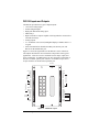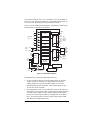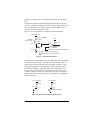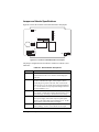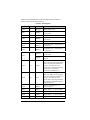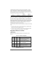
1
PK2100 C-Programmable Controller Users Manual Revision C PK2100 Users Manual Part Number 019-0014 Revision C Last revised on April 28, 2000 Printed in U.S.A. Copyright © 1998 Z-World, Inc. All rights reserved. Z-World reserves the right to make changes and improvements to its products without providing notice. Trademarks ® Dynamic C is a registered trademark of Z-World, Inc. ® Windows is a registered trademark of Microsoft Corporation PLCBus is a trademark of Z-World, Inc. ® Hayes Smart Modem is a registered trademark of Hayes Microcomputer Products, Inc. Notice to Users When a system failure may cause serious consequences, protecting life and property against such consequences with a backup system or safety device is essential. The buyer agrees that protection against consequences resulting from system failure is the buyers responsibility. This device is not approved for life-support or medical systems. All Z-World products are 100 percent functionally tested. Additional testing may include visual quality control inspections or mechanical defects analyzer inspections. Specifications are based on characterization of tested sample units rather than testing over temperature and voltage of each unit. Z-World may qualify components to operate within a range of parameters that is different from the manufacturers recommended range. This strategy is believed to be more economical and effective. Additional testing or burn-in of an individual unit is available by special arrangement. Company Address Z-World, Inc. 2900 Spafford Street Davis, California 95616-6800 USA Telephone: Facsimile: Web Site: E-Mail: (530) 757-3737 (530) 753-5141 http://www.z w orld.com [email protected] CONTENTS About This Manual vii PK2100 Overview 1-1 Getting Started 2-1 I/O Configurations 3-1 System Development 4-1 PK2100 Overview ............................................................................. 1-2 PK2100 Features· .......................................................................... 1-3 PK2110 Features ........................................................................... 1-3 PK2120 Features ........................................................................... 1-3 PK2130 Features ........................................................................... 1-3 Options and Upgrades ................................................................... 1-3 Software Development and Evaluation Tools ................................... 1-4 Initial PK2100 Setup ......................................................................... 2-2 Connecting the PK2100 to a Host PC ............................................... 2-3 Establishing Communication ............................................................. 2-3 Running a Sample Program ............................................................... 2-3 PK2100 Inputs and Outputs ............................................................... 3-2 Universal Inputs ............................................................................ 3-4 Digital Inputs ................................................................................ 3-6 High-Sensitivity Differential Analog Input .................................. 3-8 Relay Outputs ............................................................................. 3-11 Digital Outputs ............................................................................ 3-12 Analog Output ............................................................................. 3-13 Communication Interfaces .......................................................... 3-14 Programming ..................................................................................... 4-2 Gate Programming ........................................................................ 4-2 Costatements ................................................................................. 4-2 The Real-Time Kernel .................................................................. 4-2 The Five-Key System ................................................................... 4-2 Full C-Language Programming .................................................... 4-3 PK2100 Contents s iii Virtual Driver..................................................................................... 4-3 Invoking the Virtual Driver .......................................................... 4-4 Virtual Driver Services ...................................................................... 4-4 Virtual Driver Variables .................................................................... 4-6 Digital Outputs .............................................................................. 4-6 Digital Inputs ................................................................................ 4-6 Universal Inputs ............................................................................ 4-6 Timers ........................................................................................... 4-7 Downloading Code ............................................................................ 4-8 Direct Programming of the Serial Ports ............................................ 4-8 Attainable Baud Rates .................................................................. 4-9 Z180 Serial Ports .......................................................................... 4-9 Software Reference 5-1 Appendix A: Troubleshooting A-1 Driver Software ................................................................................. 5-2 Digital Input .................................................................................. 5-2 Direct Driver ............................................................................... 5-2 Virtual Driver ............................................................................. 5-2 Digital Output ............................................................................... 5-2 Direct Driver ............................................................................... 5-2 Indirect Driver ............................................................................ 5-2 Analog Input ................................................................................ 5-3 Low-Level Direct Driver ............................................................ 5-3 Calibrated Direct Driver ............................................................. 5-3 Virtual Driver for Universal Inputs ............................................ 5-4 Analog Output .............................................................................. 5-5 Direct Driver ............................................................................... 5-5 Virtual Driver ............................................................................. 5-6 High-Speed DMA Counter ........................................................... 5-6 Battery-Backed Clock ................................................................... 5-7 Liquid Crystal Display and Keypad ............................................. 5-8 EEPROM Read/Write ................................................................. 5-10 Flash EPROM Write ................................................................... 5-10 Communication ............................................................................... 5-11 RS-232 Communication ............................................................. 5-11 Support Libraries and Sample Programs .................................... 5-12 Out of the Box .................................................................................. A-2 Dynamic C Will Not Start ................................................................ A-3 Dynamic C Loses Serial Link ........................................................... A-3 PK2100 Resets Repeatedly ............................................................... A-3 Common Programming Errors ......................................................... A-4 iv s Contents PK2100 Appendix B: Specifications B-1 Appendix C: Power Management C-1 Appendix D: I/O Map and Interrupt Vectors D-1 Appendix E: EEPROM E-1 Appendix F: PLCBus F-1 Appendix G: Battery G-1 Hardware Dimensions ....................................................................... B-2 Jumper and Header Specifications .................................................... B-4 Connectors ......................................................................................... B-7 Environmental Temperature Constraints ........................................... B-7 Power Failure Interrupts .................................................................... C-2 Heat Sinking ...................................................................................... C-3 I/O Map ............................................................................................. Interrupt Vectors ............................................................................... Jump Vectors ............................................................................... Interrupt Priorities ........................................................................ D-2 D-6 D-7 D-8 PK2100/PK2120 24-V Version Calibration ...................................... E-2 PK2110/PK2130 12-V Version Calibration ...................................... E-4 Field Calibration ................................................................................ E-4 PLCBus Overview ............................................................................. F-2 Allocation of Devices on the Bus ...................................................... F-6 4-Bit Devices ................................................................................ F-6 8-Bit Devices ................................................................................ F-7 Expansion Bus Software .................................................................... F-7 Storage Conditions and Shelf Life .................................................... G-2 Instructions for Replacing the Lithium Battery ................................ G-2 Battery Cautions ............................................................................... G-3 Board Layout Index Schematics PK2100 Contents s v vi s Contents PK2100 ABOUT THIS MANUAL This manual provides instructions for installing, testing, configuring, and interconnecting the Z-World PK2100 controller. Instructions are also provided for using Dynamic C functions. Instructions to get started using Dynamic C software programming functions as well as complete C and Dynamic C references and programming resources are referenced when necessary. Assumptions Assumptions are made regarding the user's knowledge and experience in the following areas: Ability to design and engineer the target system that a PK2100 will control. Understanding of the basics of operating a software program and editing files under Windows on a PC. Knowledge of the basics of C programming. $ For a full treatment of C, refer to the following texts: The C Programming Language by Kernighan and Ritchie (published by Prentice-Hall). and/or C: A Reference Manual by Harbison and Steel (published by Prentice-Hall). Knowledge of basic Z80 assembly language and architecture. $ For documentation from Zilog, refer to any of the following texts: Z180 MPU User's Manual Z180 Serial Communication Controllers Z80 Microprocessor Family User's Manual PK2100 About This Manual s vii Terms and Abbreviations Table 1 lists and defines terms and abbreviations that may be used in this manual. Table 1. Terms and Abbreviations Term / Abbreviation Description PIO Programmable Input / Output Integrated Circuit RAM Random Access Memory RTC Real-Time Clock SIB Serial Interface Board SRAM Static Random Access Memory NMI Non-Maskable Interrupt Conventions Table 2 lists and defines typographical conventions that may be used in this manual. Table 2. Term and Abbreviation Conventions Example Description While Courier font (bold) indicates a program, a fragment of a program, or a Dynamic C keyword or phrase. // IN-01… Program comments are written in Courier font, plain face. Italics Indicates that something should be typed instead of the italicized words (e.g., in place of filename, type a file’s name). Edit Sans serif font (bold) signifies a menu or menu selection. ... An ellipsis indicates that (1) irrelevant program text is omitted for brevity or that (2) preceding program text may be repeated indefinitely. [ ] Brackets in a C function’s definition or program segment indicate that the enclosed directive is optional. byte To emphasize that certain functions must operate on 8-bit bytes, the term byte is used as a type specifier. Byte is actually a type character, not a standard C keyword. Parameters defined by byte are not standard C characters, they are 8-bit bytes. This function does not work in an application unless first declared with typedef or #define. viii s About This Manual PK2100 J1 Pin Number 1 A black square indicates pin 1 of all headers and jumpers. Pin 1 Icons Table 3 displays and defines icons that may be used in this manual. Table 3. Icons Icon $ ( Meaning Refer to or see Please contact Caution ! 7LS FD ( PK2100 Note Tip Factory Default For ordering information, call your Z-World Sales Representative at (530) 757-3737. About This Manual s ix x s About This Manual PK2100 PK2100 OVERVIEW Chapter 1 provides an overview and brief description of the PK2100 C-Programmable controller features, options, and upgrades. PK2100 PK2100 Overview s 1-1 PK2100 Overview The PK2100 series is Z-Worlds most comprehensive controller that connects directly to many sensors and peripheral devices without needing intermediate signal conditioning. A typical application for the PK2100 is the control of medium-scale production equipment, such as packaging machinery, special-purpose machine tools, or material processing systems. The PK2100 can be used to detect contact closures, count pulses, and measure analog values such as temperature or pressure. The PK2100 has two built-in relays and it can directly drive 10 external relays or solenoids. There is an analog output capability, including the 4to 20-mA loop output standard in the control industry. The PK2100 has an optional built-in keypad and liquid-crystal display (LCD). There is a PLCBus expansion bus connector that allows external expansion of the input/output capabilities or the addition of interface devices designed by the user. The PK2100 has serial communication capability suitable for communicating with other controllers one at a time or in a plant-wide network. It supports both RS-232 and RS-485/RS-422 serial communication modes. PLCBus Expansion Bus Connector Screw Connectors Keypad menu item setup F1 Screw Connectors 2 × 20 LCD F2 field run up down F3 F4 del help init add RS-232 Connector Figure 1-1. PK2100 C-Programmable Controller 1-2 s PK2100 Overview PK2100 PK2100 Features Seven fixed digital inputs Six universal inputs One high-gain differential analog input Ten high-current outputs capable of driving inductive loads such as solenoids and relays Two SPDT relays Two analog outputs 2 x 20-charcter LCD screen (backlighted display available) and 2 x 6 keypad PLCBus port One RS-232 port and one RS-232 or RS-485/RS-422 port Rugged enclosure Battery-backed RAM up to 512 kbytes EPROM up to 512 kbytes for holding program and data Optional flash EPROM to replace standard EPROM Battery-backed time/date clock Lithium button battery, which lasts about 10 years in normal use, to provide power for the time/date clock and the battery-backed memory when no external power is supplied to the unit; option for nickelcadmium battery or a super capacitor for battery backup Watchdog timer Power failure warning interrupt EEPROM, standard 512 bytes, to hold factory-set calibration constants and user configuration data of a more permanent nature than data held in the battery-backed RAM PK2110 Features The PK2110 is a 12-volt version of the PK2100. PK2120 Features The PK2120 is a PK2100 without the enclosure, the keypad or the LCD. PK2130 Features The PK2130 is a 12-volt version of the PK2120. Options and Upgrades 9.216-MHz clock upgrade can be factory installed. 128-kbyte flash EPROM can be factory installed. 128-kbyte or 512-kbyte SRAM can be factory installed. Backlit-character LCD is available for the PK2100 and the PK2110. $ Appendix B provides detailed specifications for the PK2100. PK2100 PK2100 Overview s 1-3 Software Development and Evaluation Tools Dynamic C, Z-Worlds Windows-based real-time C language development system, is used to develop software for the PK2100. The host PC downloads the executable code through the PK2100s RS-232 port to one of the following places: battery-backed RAM, ROM written on a separate ROM programmer and then substituted for the standard Z-World ROM, or optional flash EPROM, which may be programmed or reprogrammed without removing it from the controller. This allows fast in-target development and debugging. A PK2100 Development Kit contains the manual, schematics, programming cable, power supply, 128-kbyte flash EPROM and a demonstration board to simulate input/output. Dynamic C reference manuals provide complete $ Z-Worlds software descriptions and programming instructions. 1-4 s PK2100 Overview PK2100 GETTING STARTED Chapter 2 provides instructions for connecting the PK2100 to a host PC and running a sample program. PK2100 Getting Started s 2-1 Initial PK2100 Setup When the PK2100 powers up, it reads its board jumpers, the keypad, if any, and the contents of the EEPROM to determine its mode of operation. The following modes of operation are available: 1. Run a program stored in battery-backed RAM. 2. Program at 19.2 kbaud using the RS-232 port. 3. Program at 38.4 kbaud using the RS-232 port. The keypad (Figure 2-1) may be used to set the mode. Hold down the MENU/setup key and one other key (FIELD/run, UP/pgm 19.2, or DOWN/pgm 38.4) simultaneously. The unit will beep to acknowledge the change of operating mode. menu item setup field up run pgm 19.2 down help init pgm 38.4 Figure 2-1. PK2100 Keypad ! The watchdog timer must be enabled when the keypad is used to set the mode. A jumper installed on jumper block J4 overrides any keypad settings. The jumper block must be used when a keypad is not available, for example, in the PK2120 controller. Figure 2-2 illustrates the jumper configurations. Program at Program at Run program at 19.2 kbaud at 38.4 kbaud in RAM J4 J4 J4 Figure 2-2. PK2100 Jumper Configurations for Programming 2-2 s Getting Started PK2100 Connecting the PK2100 to a Host PC 1. Make sure the PK2100 power source is not connected. 2. Connect the PK2100 to the host PCs RS-232 serial COM port. A 9-pin to RS-232 phone plug adapter is included with the developers kit. 3. Connect the red-tagged lead from the 24-volt (or 12-volt) power supply to the +24-volt screw connector. Connect the other power supply lead to the GND screw connector. 4. Plug the power supply into a wall socket. The North American version of the PK2100 developers kit comes with a 24-volt D.C. power supply. International users and users of PK2110/PK2130 controllers, which are designed for 12 volts, must provide an appropriate power supply. The PK2100 is now ready to be programmed. Establishing Communication Communication between the PC and the PK2100 becomes possible once the hardware is connected and the Dynamic C software has been installed. Double-click the Dynamic C icon to start the software. Note that the PC attempts to communicate with the PK2100 each time Dynamic C is started. No error messages are displayed once communication is established. See Appendix A, Troubleshooting, if an error message such as Target Not Responding or Communication Error appears. Once the necessary changes have been made to establish communication between the host PC and the PK2100, use the Dynamic C short-cut Ctrl Y to reset the controller and initiate communication. $ ! Running a Sample Program 1. Open a sample program located in Dynamic C subdirectory. SAMPLES\CPLC. $ PK2100 See Appendix A, Troubleshooting, if an error message such as Target Not Responding or Communication Error appears. Getting Started s 2-3 2. Compile the program by pressing F3 or by choosing Compile from the Compile menu. Dynamic C compiles and downloads the program into the PK2100s flash memory. 3. Run the program by pressing F9 or by choosing Run from the Run menu. 4. Press Ctrl Z to stop execution of the program. 5. If needed, press F9 to restart execution of the program. 2-4 s Getting Started PK2100 I/O CONFIGURATIONS Chapter 3 discusses how to configure the available inputs/outputs in the PK2100 controller. PK2100 I/O Configurations s 3-1 PK2100 Inputs and Outputs The PK2100 provides these types of inputs/outputs: Universal analog inputs. Protected digital inputs. High-gain differential analog input. SPDT relays. High-current driver outputs capable of driving inductive loads such as solenoids and relays. Analog outputs. 2 × 20-charcter LCD screen (backlighted display available) and 2 × 6 keypad. Serial communication channels: PLCBus port, RS-232 port, and RS-232 or RS-485/RS-422 port. Figure 3-1 shows the signal names of the PK2100s screw connectors. The chapter describes the various interfaces and presents some typical applications. There are 50 screw terminals used for input, output, and power connections. In addition, there are two connectors on the sides of the unit: a modular phone jack connector for the RS-232 port, and a 26-pin connector for the PLCBus expansion port. +10-V ref +5 V GND U1 U2 U3 U4 U5 U6 GND D1 D2 D3 D4 D5 / C1A D6 / C1B D7/ C2A GND GND Tx RS-485/ Tx+ RS-422 Rx Rx+ C2B+ C2B Digital Inputs Universal Inputs DC in K GND O1 O2 O3 O4 O5 O6 O7 O8 O9 O10 GND A/D A/D+ DAC UEXP NC1 COM1 NO1 NC2 COM2 NO2 GND Digital Outputs PLCBus Relay 1 Relay 2 RS-232 Figure 3-1. PK2100 Pin Layout 3-2 s I/O Configurations PK2100 The connector labeled +10-V ref is nominally 7 volts for the PK2110/ PK2130 12-volt versions of the PK2100. The connector labeled DC in is 12 or 24 volts, depending on the specific PK2100 model. Figure 3-2 shows a PK2100 block diagram. The PK2100s board layout and schematic are included in this manual. U1 U2 Universal Inputs U3 Real-Time Clock U4 Battery U5 Gain Input A/D+ UEXP DAC O1 O2 O3 O4 O5 O6 O7 RAM U6 High- DAC Output Z180 HighCurrent Digital Output K EPROM NC1 COM1 NO1 NC2 Relay 2 COM2 NO2 HighO8 Current O9 Digital O10 Output Relay 1 A/D D5 D6 D7 D1 D2 D3 D4 EEPROM RS-232 Digital Input Beeper PLCBus Expansion C1A C1B DC in LCD & Keypad C2A C2B+ C2B Counter Inputs Rx Rx+ Tx Tx+ RS-485/RS-422 Figure 3-2. PK2100 Block Diagram The PK2100 has the following input/output interfaces: 1. Six universal inputs that may be used as analog inputs (to measure voltage, current, or resistance) or as digital inputs (to measure a voltage compared to a specific threshold voltage or to softwarespecifiable high and low thresholds). The universal inputs accept 0 10 volts with 10-bit resolution. 2. Seven digital inputs with a 2.5-volt threshold. Three of the inputs are dual-purposethey function either as general-purpose digital inputs or as counter inputs. When serving as counter inputs, the three inputs provide two counter inputs capable of counting pulses at 100 kHz or more. The counter inputs can also be used to measure pulse widths and other pulse timing characteristics. PK2100 I/O Configurations s 3-3 3 One high-sensitivity differential analog input. Normally, the high-sensitivity range is 01 volts, but the input gain can be changed by installing different input resistors on the operational amplifier. When the positive side of the differential input is more than 1 volt, its voltage can be measured by the universal input with which it is coupled. This input is suitable for connection to resistance bridges. 4. Two relay-contact outputs (NO, NC, COM for each relay). The relays are rated for 3 amps at 48 volts. Contact-protection devices may be installed. 5. Ten high-current outputs suitable for driving relays, stepping motors, or solenoids. These outputs can sink approximately 300 milliamps each at up to 48 volts, subject to total heat dissipation restrictions for the integrated-circuit driver. 6. One analog output (DAC), which may be a voltage output (010 volts for PK2100/PK2120 and 07 volts for PK2110/PK2130) or a current output (020 mA for PK2100/PK2120 and 015 mA for PK2110/ PK2130). A second analog voltage output (UEXP) is available when the universal inputs are used as fixed-threshold digital inputs. 7 Communication interfaces including a full-duplex RS-422/RS-485 serial port that can operate asynchronously at up to 38,400 baud, and an RS-232 serial port with two handshaking lines that can operate at up to 38,400 baud. A second RS-232 port can be configured as a substitute for the RS-422/RS-485 port by changing board jumpers, but it will have no handshaking lines. There is also a 26-pin connector to Z-Worlds PLCBus expansion bus for customer-designed devices or Z-World PLCBus expansion devices. Universal Inputs The universal interface comprises six analog inputs (U1U6) with a measurement range of 010 volts (07 volts for PK2110/PK2130). An additional universal input channel (A/D+) is available when it is not in use as part of the high-gain input. A universal input may be read either as an analog input (by taking an analog reading) or as a digital input by comparing the voltage at the input with a threshold. Software provided by Z-World can be used to compare the input voltage to a single fixed threshold or to two software-specified thresholds. Single Threshold. A digital 1 results when the voltage is above the threshold. Otherwise a digital 0 results. Dual Threshold. A digital 1 results when the voltage is above the high threshold. A digital 0 results when the voltage is below the low threshold. Otherwise, the software reports no change. Z-Worlds virtual driver 3-4 s I/O Configurations PK2100 software (see Chapter 4, System Development) provides the two thresholds. The universal inputs are protected against overloads between -48 and +48 volts. The analog resolution is 10 bits, providing approximately 1024 steps over the range 010 volts (07 volts for PK2110/PK2130). Its sensitivity is about 10 millivolts per step. Figure 3-3 shows a schematic of a single universal input channel. +10-V reference +3.3-kΩ excitation +resistor Jumpers (H4, H5, H6) Input 22 kΩ 0.01 µF 4.7 kΩ VCC + 10 kΩ comparator LM339A UEXP value or fixed reference (RR) 430-Ω resistor, 420 mA loop, channel 6 only. Connect H5:78 Figure 3-3. Universal Input Channel Each input uses a comparator driven by the signal and by an internal DAC to measure the input voltage. The input resistor and capacitor filter out high-frequency noise and provide protection against overloads. Clamp diodes in the LM339A provide additional protection against overload. The input has a high D.C. impedance unless one of the jumpers is connected. If the excitation resistor is connected, the circuit provides an excitation voltage or current to an external device. This is convenient for measuring an external resistance such as a potentiometer or a temperature sensor (Figure 3-4). +10-V reference 3.3 kΩ +10-V reference 3.3 kΩ 8 kΩ Temperature Sensor Figure 3-4. Measuring Variable External Resistance PK2100 I/O Configurations s 3-5 Multiple contacts may be connected with external resistors to a single universal input (Figure 3-5). +10-V ref +10-V ref 3.3 kΩ 4 kΩ 1 kΩ (a) Multiple Contacts (closest has priority) 2 kΩ 3.3 kΩ 1 kΩ (b) Muliple Contacts Resolvable Individually Figure 3-5. Use of External Resistors to Connect Multiple Contacts to Single Universal Input Digital Inputs The seven digital inputs accept an input voltage with a digital threshold at approximately 2.5 volts. The inputs are protected against overload over a range from -48 to +48 volts. These inputs are convenient for detecting contact closures or sensing devices with open collector transistor outputs. Logic-level outputs can also be detected as long as they are supplied from CMOS logic outputs guaranteed to swing to at least 3.5 volts. Three of the digital inputs are shared as inputs to the high-speed counters. Figure 3-6 shows a digital input. The RC circuit helps to stabilize the input, but note the 0.2-millisecond RC time constant, which affects signals faster than 5 kHz. While it may be tempting to disable the capacitor with a jumper, this is not recommended because the signal may be degraded. +5 V 10 kΩ 22 kΩ Input 0.01 µF Digital Input Figure 3-6. PK2100 Digital Input 3-6 s I/O Configurations PK2100 Three of the digital inputs also serve as counter inputs. In addition, there is a special differential counter input. The counter inputs are arranged as shown in Figure 3-7. +5 V C1A C1B +5 V +5 V J8: 7-8 J8: 9-10 /DREQ0 Counter 1 /DREQ1 Counter 2 CKA1 C2A C2B+ + C2B C2B U34, RS-485 receiver Figure 3-7. Digital Inputs Used As Counter Inputs The counters count on a negative-going edge. Each counter has two inputs, which are symmetrical in that one can be used as a gate and the other can be used as a count input. The RS-485 receiver input can be used as a digital input by attaching one side of it to the desired threshold voltage. This input can be used as a true differential input for such devices as inductive pickups. It has a commonmode voltage range from -12 to +12 volts with an input hysteresis of 50 millivolts. An internal jumper can connect the signal from input/output procesor CKA1, which is controlled by the second (RS-485) serial ports hardware. CKA1 can be set to count pulses at 100 kHz or more down to a few hundred hertz. The counters are implemented by using the DMA channels of the Z180 microprocessor. The maximum count speed is more than 100 kHz. The DMA channel can be programmed to store a byte from an input/output port to memory for each count, if desired. This byte can be the least significant byte of the internal programmable counter (PRT), which allows the count edge to be localized in time. This feature can also determine the PK2100 I/O Configurations s 3-7 exact time, within a few microseconds, at which an event occurs by programming the DMA channel to store one byte and then interrupt the count. The interrupt routine can read the most significant part of the PRT counter and any software extension of this counter. In general, the maximum count is 65,536, which can be extended by software to larger counts if the counting speed is not higher than about 10 kHz. The capabilities of the counters are summarized below. Counters measure the time at which a negative edge occurs with a precision of a few microseconds. The measurement can be repeated hundreds of times per second. A minimum time must occur between successive events to allow for interrupt processing. Counters measure the width of a pulse by counting (up to 65,536) at a rate from more than 100 kHz to 300 Hz. This provides 16-bit accuracy in the measurement of pulse widths. Counters count negative-going edges for up to two channels. The maximum count for high-speed counting (5 kHz to more than 100 kHz) is 65,536. The maximum count for low-speed counting is unlimited. High-Sensitivity Differential Analog Input One high-sensitivity analog input is available. This input has a differential input with a gain of 10 compared to the universal input. This input is useful for devices requiring higher input sensitivity, for example, thermistors or RTDs in a bridge. Although the high-sensitivity input has 10 times the gain and accuracy, the dynamic range is necessarily 10 times less, since the number voltage steps available from the conversion (1024) does not change. Figure 3-8 shows the high-sensitivity input circuit. 470 kΩ RP5B H7 AD+ AD 47 kΩ R11 47 kΩ R5 + to Comparator 7 470 kΩ RP5A 7th Universal Input to Comparator 8 Figure 3-8. High-Sensitivity Differential Analog Input 3-8 s I/O Configurations PK2100 The gain at the plus and minus inputs is 10 when jumper H7 is installed. The gain of the plus input becomes higher (11) when H7 is removed. This has the effect of skewing the output from a nulled bridge circuit to the middle of the measurement range. Such a bridge circuit is shown in Figure 3-9 below. When the bridge is nulled, both inputs are equal to 5 volts. The output voltage of the input amplifier with H7 removed is 5 × (11 - 10) = 5 volts. This is in the middle of the 10-volt measurement range of Variable element (thermistor, RTD, etc.) +10-V reference to High-sensitivity differential input Figure 3-9. Nulled Bridge Circuit for Measuring High-Sensitivity Differential Analog Input 010 volts. The bridge makes it possible to detect changes of ±0.04 percent in the value of the variable-resistor element when the gain is 10. A change of only ±0.2 percent can be detected without a bridge. g = 10 = R5 + RP5A RP5B × Jumper H7 installed R5 RP5B + R11 The gain for the negative input, AD, is given by RP5A/R5. The gain for g = 11 = R5 + RP5A × (1) . R5 Jumper H7 not installed the positive input, AD+, is given by: or The calibration gain and offsets are stored in the EEPROM (see Appendix E). The output voltage, y, is given by y = a1 × (x1 + a0) - b1 × x2 where x1 and x2 are the positive and negative inputs, respectively, a1 is the positive-side gain, a0 is the positive-side offset, and b1 is the negative-side gain. Configurations 3-9 b1 is also equal to the calibrated value of a1I/O (with Jumper H7snot connected) minus 1, that is, b1 = a1 - 1. PK2100 Note that If the negative input x2 is tied to ground, the equation becomes y = a1 × (x1 + a0) or, solving for x1, x1 = y - a0 . a1 This equation returns the input voltage, given the output. The function up_higain(1) returns this value (with Jumper H7 removed). If the output of the operational amplifier is out of range (x1 input above 1 volt, y output above 10 volts), the value of a direct measurement of x1 is returned. This is less accurate by a factor equal to the gain ratio. Solving this equation for (x1 - x2) in terms of y and x1 yields (x1 − x 2 ) = a y a1 − − 1 × x1 − a 0 × 1 b1 b1 b1 . The function up_higain(2) returns this value (with Jumper H7 removed). This is the difference between inputs x1 and x2 in terms of y and x1, both of which can be measured directly. The accuracy with which the difference voltage is measured is approximately 10 times greater than for the regular universal input channels: 1 millivolt instead of 10 millivolts. Change resistor R5, and possibly R11, to change the gain of the high-gain input. These 47-kΩ resistors are factory-installed for a gain of 10 (or 11 if Jumper H7 is removed). A smaller resistor will increase the gain. For example, changing both the R5 and R11 resistors to 10 kΩ will increase the gain to 47 (or 48 with Jumper H7 removed). When differential inputs are desired, it is preferable to operate with H7 removed since the gain difference between the positive and negative inputs will be exactly 1 and will not depend on a balance between resistors, making the output 5 volts when both differential inputs are 5 volts. As the gain is increased, it becomes necessary to use an operational amplifier with a more stable offset voltage than the LM324, which has considerable drift over temperature. The Linear Technology LM1014 is suitable for gains up to 100 or more. The negative input has a low input impedance compared to the positive input when H7 is removed. If R5 is decreased to increase the gain, this impedance becomes even lower. When a bridge is used, the finite impedance of the negative input will change the gain slightly. 3-10 s I/O Configurations PK2100 The gain for a bridge such as +10 V R1 R2 V V0 47 kΩ R11 47 kΩ R5 + 470 kΩ RP5A would be 1 . R5 R5 g = g0 × 1 – + 1+ R2 R1 The change in gain for the input (V V0) is given by the above formula. If R5 is 47 kΩ and R1 and R2 are each 350 Ω, then the gain is reduced by the factor 1 = 0.9962 1− 47,000 47,000 + 1+ 350 350 or about 4 parts in 1000. Relay Outputs The PK2100 has two relays. Each relay (Figure 3-10) is single pole, double throw. The rated current is 3 A and the rated voltage is 48 V. Optional metal-oxide varistors (MOV) may be installed on the board to protect the contacts. When the voltage across the contact exceeds the trigger voltage of the MOV, the MOV acts as a short circuit, preventing or minimizing sparking and arcing. NC +24 V A COM B NO Figure 3-10. PK2100 Relay PK2100 I/O Configurations s 3-11 The relay output signals are routed through the U35 high-current driver chip. Digital Outputs The PK2100 has 10 digital outputs (O1O10). Seven of the outputs belong to one high-current driver chip (U26) and three belong to another chip (U35). These outputs can drive inductive loads such as relays, small solenoids, and stepping motors. Outputs O1O7 on U26 use a common bus (K) for the protective diodes. Thus, it is possible to use a power supply for these outputs other than the power supply for the PK2100. All loads connected to the same group of drivers must use the same power supply so the diodes can return inductive spikes to the same power supply. Refer to Figure 3-11. External power supply (up to 48 V) Inductive load K Digital output channel, O1O7 Figure 3-11. Routing External Power Supply for PK2100 Digital Outputs If the PK2100s power supply (DC in, 12 or 24 volts) is used, route K to the power supply by connecting jumper H11. Refer to Figure 3-12. DC in Inductive load Digital output channel, O1O7 DC in H11 K Figure 3-12. Routing PK2100 Internal Power Supply for Digital Outputs 3-12 s I/O Configurations PK2100 The diodes on U35 for outputs O8O10 use the PK2100s power supply directly. D.C. in D.C. in Inductive load Digital output channels O8O10 Figure 3-13. Routing PK2100 Power Supply for Digital Outputs O8O10 The drivers used are the Motorola MC1413B or the equivalent Texas Instruments ULN2003. One drives outputs O1O7, and the other drives outputs O8O10, the onboard relays and the beeper. Each driver chip can dissipate a maximum of 1.25 watts when the ambient temperature is 60°C. Each output consumes power, depending on the current, as follows. 100 mA 200 mA 350 mA 0.10 W 0.25 W 0.50 W This limits the maximum current to approximately 150 milliamps per output if all outputs are turned on at the same time for a 100 percent duty cycle. The maximum current for any single output is 500 milliamps. Analog Output One analog output (DAC) is provided. With Pins 2-3 on Jumper J7 connected, the output can be a voltage (010 volts for PK2100/PK2120 and 07 volts for PK2110/PK2130); connecting Pins 1-2 on Jumper J7 turns the output into a current output suitable for driving current loops at 420 mA. The analog output will drive 20 milliamps (15 milliamps for PK2110/PK2130) up to 470 Ω with a resolution of 10 bits. Another 10-bit analog output channel (UEXP) is available if it is not being used to support the universal inputs. Communication Interfaces The PK2100 comes with a full-duplex RS-422/RS-485 serial port that can operate asynchronously at up to 38,400 baud (57,600 with the optional 9.216-MHz clock upgrade). An RS-232 serial port with two handshaking PK2100 I/O Configurations s 3-13 lines can also operate at up to 38,400 baud (57,600 with the optional 9.216-MHz clock upgrade). A second RS-232 port can be configured as a substitute for the RS-422/ RS-485 port by changing board jumpers, but it will have no handshaking lines. Pins 3-4 and 5-6 on Header 8 are connected to enable RS-422/ RS-485 communications. Remove these jumpers and connect Pins 1-2 on Header 8 to enable the second RS-232 output. The RS-232 output pin will be TX-, and the input will be RX-. RX+ must be tied to ground. The jumper arrangements are shown in Figure 3-14. The PK2100 has a 26-pin connection to allow access to Z-Worlds PLCBus expansion bus for customer-designed devices or Z-Worlds PLCBus expansion devices. RS-422 RS-485 RS-232 H8 H8 1 2 1 2 3 4 3 4 5 5 6 5 6 Figure 3-14. H8 Jumper Configurations 3-14 s I/O Configurations PK2100 SYSTEM DEVELOPMENT Chapter 4 describes the programming support for the PK2100. PK2100 System Development s 4-1 Programming Z-world supports program development for the PK2100 in a variety of ways. Support for some of these stems from a virtual driver, which monitors the PK2100s ports and provides a set of virtual latches, timers, counters, function keys and two DAC analog outputs. Gate Programming Gate programming is a quick and easy way to program the PK2100s inputs and outputs. The logic elements are summarized in Table 4-1. Table 4-1. Gate Programming Logic Elements External Internal Seven digital inputs Thirty memory latches Six universal inputs Ten on-delay timers Ten digital outputs Five countdown counters Two relay outputs Four special function keys Discrete digital-to-analog outputs An operator updates the parameters supported by these logic elements using the five-key system. Gate programs can be downloaded or uploaded serially through the RS-232 connection to a PC. ! Gate programming is not C programming. It is done with an application program, written in C, that modifies the parameters of the virtual driver. Support functions for gate programming may be found in the subdirectory LIBRARY\GATE_P.LIB. The programs SCAN.C and GATER.C in SAMPLES\CPLC are examples of gate programming. Costatements Costatements, formerly called function blocks, implement cooperative multitasking, and use the virtual driver. The Real-Time Kernel The real-time kernel allows a preemptive multitasking system to be developed. The Five-Key System The five-key system implements a user interface to the software using the PK2100s keypad and liquid crystal display. 4-2 s System Development PK2100 Full C-Language Programming Full C-language programming may access all the features available in Dynamic C and its libraries. Gate programming and costatements use Z-Worlds virtual driver. Full Dynamic C programming, of course, may include any method or combinations of methods. Virtual Driver The virtual driver is a software package activated by a periodic interrupt every 25 milliseconds and provides certain services to the application programmer. The virtual driver provides the following services. Running real-time second and millisecond clocks. Scanning the universal inputs to compare them against preset thresholds. Scanning the digital inputs and setting digital outputs. Providing any number of virtual watchdog timers. Providing clock drive for the optional real-time kernel. Providing control for an audible beeper. Providing a driver for the keypad. Providing a driver for the liquid crystal display. The following switches turn off the services of the virtual driver. If used, they must precede driver calls. Leave the switch undefined to avoid disabling the service. #define NOUNIVERSAL Disable the virtual driver for digital inputs, universal inputs, digital outputs and relays. #define NOTIMERS Disable the virtual timers. The virtual timers are software timers, useful in ladder logic programming and gate programming. #define NOLCD Disable the liquid crystal display (LCD). This directive will prevent the initialization of the LCD. Commands to the LCD have no effect unless the LCD has been initialized. PK2100 System Development s 4-3 The following preprocessor variables control features of the virtual driver. #define N_WATCHDOG nn Specify the number of virtual watchdog timers. Each virtual watchdog has a counter that has to be reloaded. If the counter for any virtual watchdog counts down to zero, a hardware reset is forced. To reload a virtual watchdog, type up_wdoghit( int watchdog, byte count ) where count is the number of 25-millisecond ticks to countdown. A virtual watchdog wdog can be monitored, if necessary, by reading the internal variable lc_wdogarray[wdog-1]. The program VWDOG.C in the subdirectory SAMPLES\CPLC illustrates the use of virtual watchdog timers. #define RUNKERNEL Request the real-time kernel. It will be initialized. #define KEYREQUEST nn Request a real-time kernel task when a key is pressed. The sample program SAMPLES\CPLC\VWDOG.C illustrates the use of this directive. Invoking the Virtual Driver Call uplc_init() from the main function to invoke the virtual driver. This call will initialize the following items: Variables for the virtual driver. Virtual watchdog timers (if requested). The liquid crystal display (unless disabled). The real-time kernel (if requested). The timer that runs the background routine. The program must periodically hit the (hardware) watchdog uplc_init() to keep it from timing out. Virtual Driver Services up_beep( int milliseconds ) Beeps the built-in beeper for the number of milliseconds specified. up_beepvol( int code ) Sets beeper volume. The code is 0, 1, or 2, and corresponds to beeper off, low, or high volume. 4-4 s System Development PK2100 lcd_printf( long cursor, char *fmt, arg... ) Print on the liquid crystal display screen. The variable cursor determines the position of the cursor before and after the string of characters determined by the format *fmt and the arguments (arg...) is printed according to traditional printf conventions. The cursor variable is a long integer consisting of four bytes, Y1, X1, Y2, X2, where Y1 is in the most significant byte. The pair Y1, X1 is the position of the cursor before writing and Y2, X2 is where the cursor will be positioned after writing. The upper four bits of Y2 specify whether the cursor will be left on (1) or off (0) after the print is complete. If *fmt is a null string, then only cursor positioning will take place. Lines On a 2 × 20 screen (Y values) are numbered 0 and 1. Columns (X values) are numbered 0...19. A screen with four lines has lines numbered 03. The function lcd_printf is not reentrant. If it is used in a multitasking environment, it is necessary to restrict lcd_printf to only one task at a time. Several utility routines make this possible. The following routines save and restore the contents of the liquid crystal display screen. The program must have the token to use these routines in a multitasking environment. lcd_savscrn( struct lcd_scrn *s ) lcd_resscrn( struct lcd_scrn *s ) The following routines erase the screen or a line on the screen. The user must have the token to call these routines in a multitasking environment. lcd_erase() lcd_erase_line( int line ) // line is 0 or 1 A copy of the display contents and the location of the cursor is updated in memory whenever lcd_printf prints to the liquid crystal display. The function lcd_savscrn copies this image to a user-specified save area. The function lcd_resscrn copies the screen save area back to the screen and the image copy. A task can use these routines to interrupt another task using the liquid crystal display, save the image, use the liquid crystal display, restore the image, and return the liquid crystal display to the original task. PK2100 System Development s 4-5 Virtual Driver Variables The variables described here are defined in CPLC.LIB. The virtual driver updates the input variables every 25 milliseconds to reflect the state of the hardware inputs and sets the hardware outputs based on the state of its output variables. ! The virtual driver does not change input variables unless the hardware input has the same value for at least two ticks of the virtual driver. Digital Outputs The 10 digital outputs and the two relay outputs are represented by the following variables: RELAY1, RELAY2 OUT1, OUT2...OUT9, OUT10 Storing a 1 in these variables causes the corresponding output to be energized on the next virtual driver tick. Storing a 0 clears the corresponding output. Digital Inputs Seven variables represent the seven digital inputs: DIGIN1, DIGIN2...DIGIN6, DIGIN7 These variables are updated every virtual driver tick (25 ms). They are set to either 1 or 0 depending on the state of the physical input. A 1 corresponds to an input value of at least 2.5 volts. Universal Inputs The universal inputs are represented by these variables: U1IN, U2IN, U3IN, U4IN, U5IN, U6IN They are updated to 1 or 0 depending on the relationship of the analog input to preset thresholds. A high threshold and a low threshold are associated with each universal input variable. These are the levels at which the flags U1IN, U2IN, ... are switched. U1LOW,U1HIGH, U2LOW,U2HIGH, ... U6LOW,U6HIGH The way the universal inputs are interpreted is determined by setting these thresholds. 4-6 s System Development PK2100 Timers There are 10 virtual timers. Each timer has an input flag, an output flag, and a reload value. T1IN, T2IN ... T10IN // input flags T1O, T2O ... T10O // output flags T1RLD, T2RLD ... T10RLD // reload values When a timer input (for example, T1IN) goes from 0 to 1, the counter starts counting from the reload value (for example, T1RLD) down, one count every virtual driver tick (25 milliseconds). The output flag (T1O) is set to 1 when the count reaches zero. The output is forced to zero whenever the input is set to zero. TxIN Counter TxO Figure 4-1. Timer Ouput Variation Over Time with Timer Input and Counter PK2100 System Development s 4-7 Downloading Code A program may be downloaded to the PK2100 via a serial or other communications link. A related problem is loading programs to EPROM, RAM, or an external mass storage device for execution. The basic method for downloading starts with writing a monitor program that is burned into EPROM. This monitor program serves as a master controller to load and start execution of the programs and to regain control when the executed program finishes. The monitor program must also gain control when the board is reset through hardware, either by power-on, watchdog time-out, or the reset key. An external hardware reset line may be installed to allow the computer that is downloading the program to be able to force a hardware reset of the PK2100. Connect Pins 2 and 3 on Jumper J11 to use the CTS0 line from the 6-pin phone jack to control external resetting of the PK2100. However, the handshaking line for the RS-232 port will be lost. To be safe, tie the /CTS0 line of the RS-232 port to ground to continue to use the RS-232 port for communication. $ Refer to the Dynamic C manual for a discussion on memory mapping and remote downloading and execution of code. Direct Programming of the Serial Ports The Z180 Technical Manual and the Z80 SIO Technical Manual, available from Zilog, Inc., in Campbell, California, provide detailed information to plan extensive use of the serial ports and synchronous communications. Z-World provides just a few low-level utility functions: int sysclock() int z180baud( int clock, int baud ) The sysclock function returns the clock frequency in units of 1200 Hz, as read from the EEPROM. The clock frequency was stored at location 108H at the factory. The z180baud function returns the byte to be stored in CNTLB0 or CNTLB1, considering only the bits needed to set the baud rate. The clock and baud rate must be specified in units of 1200 Hz. Thus, a 9.216-MHz clock is expressed by 7680, and 19,200 baud is expressed by 16. The return value is 1 if the baud value cannot be derived from the given clock frequency. Each serial port appears to the CPU as a set of registers. Each serial port can be accessed directly with the inport and outport library functions, using the symbolic constants for Address 0009 in Table D-1, Appendix D. 4-8 s System Development PK2100 For example, to read and write from serial port 0: char ch; ch = inport( RDR0 ); outport( TDR0, ch ); Ports may be polled or interrupt-driven. The interrupt vectors are given in Table D-4, Appendix D. Attainable Baud Rates The serial ports built into the Z180 can generate standard baud rates when the clock frequency is 6.144 MHz or 9.216 MHz or a small multiple, for example, 3.072, 4.608, 6.144, 9.216, or 12.288 MHz. A crystal is stamped with twice the clock frequency. Z180 Serial Ports The Z180 has two independent, full-duplex asynchronous serial channels, with a separate baud-rate generator for each channel. The baud rate can be divided down from the microprocessor clock or from an external clock for either or both channels. The serial ports have a multiprocessor communications feature that can be enabled. When enabled, an extra bit is included in the transmitted character (where the parity bit would normally go). Receiving Z180s can be programmed to ignore all received characters except those with the extra multiprocessing bits enabled. This provides a 1-byte attention message that can be used to wake up a processor without the processor having to monitor (intelligently) all traffic on a shared communications link. Figure 4-2 shows the configuration for Serial Channel 0. The configuration for Serial Channel 1 is similar, but modem control lines RTS1 and DCD0 are not available. Five of the seven registers shown are accessible directly as internal registers. Microprocessor Internal Bus RXA0 RDR0 TDR0 RSR0 TSR0 Shift Register In RTS0 CTS0 DCD0 CNTLA0 CNTLB0 Baud-Rate Generator TXA0 Shift Register Out CLKA0 STAT0 Figure 4-2. Z180 Serial Channel 0 Configuration PK2100 System Development s 4-9 The serial ports may be polled or interrupt-driven. A polling driver tests the ready flags (TDRE and RDRF) until a ready condition appears (transmitter data register empty or receiver data register full). If an error condition occurs on receive, the routine must clear the error flags and take any appropriate action. If the CTS line is used for flow control, transmission of data is automatically stopped when CTS goes high because the TDRE flag is disabled. This prevents the driver from transmitting more characters, because it thinks the transmitter is not ready. The transmitter will still function with CTS high, but care must be exercised since TDRE is not available to synchronize the loading of the data register ( TDR). An interrupt-driven driver works with the program enabling the receiver interrupt as long as it wants to receive characters. The transmitter interrupt is enabled only while characters are waiting in the output buffer. When an interrupt occurs, the interrupt routine must determine the cause: receiver data register full, transmitter data register empty, receiver error, or DCD0 pin high (channel 0 only). None of these interrupts is edgetriggered. Another interrupt will occur immediately, if the interrupts are re-enabled without disabling the condition causing the interrupt. The signal DCD0 is especially treacherous because it cannot be disabled when the receive interrupts are on. In most designs, the DCD0 line should be connected directly to ground, thus taking it out of the picture. 4-10 s System Development PK2100 SOFTWARE REFERENCE Chapter 5 presents information on the Dynamic C software drivers and communication software for the PK2100. PK2100 Software Reference s 5-1 Driver Software Drivers in the Dynamic C software library make it easy to communicate with the PK2100 inputs and outputs. Drivers may be direct or indirect. A direct driver immediately reads or writes to the controlled hardware. An indirect driver uses intermediate variables. Z-Worlds virtual driver is a periodically called interrupt service routine that connects the hardware with intermediate variables. Drivers may be low-level drivers that return, send, or transmit values when the values are received or presented by the interface. High-level drivers modify the inputs or outputs in some way, such as by introducing calibration, hysteresis or averaging. Indirect, high-level drivers are preferred because they eliminate any concern about the technical details of the input/output interface. The price for this convenience is a slight loss of speed and efficiency. Digital Input Direct Driver int up_digin( int channel ) Gets the value at the specified digital input channel (17). The function returns 1 when the channel is high and 0 when the channel is low. Virtual Driver Reference the parameters DIGIN1, DIGIN2, DIGIN3, DIGIN4, DIGIN5, DIGIN6, and DIGIN7. For example, heater = DIGIN1 || DIGIN2; These variables take the value 1 if the input is high (greater than 2.5 volts) and 0 if the input is low. The parameter value changes only if the new value remains the same for 2 ticks (2550 ms) of the virtual driver. Digital Output Direct Driver int up_setout( int channel, int value ) Passes channel number 110 and value 0 for OFF, 1 for ON. If channel is 11 or 12, relay 1 or 2 is switched. Indirect Driver Set the variables OUT1, OUT2, OUT3, ... OUT9, OUT10 to a value of 0 to turn the output off, or to a value of 1 to turn the output on. Outputs pull low when turned on. The variables RELAY1 and RELAY2 control the relay contacts. 5-2 s Software Reference PK2100 Analog Input The A/D system relies on software calibration, using calibration constants stored in the system EEPROM. Uncalibrated values are in the range 01023, with each count representing approximately 10 millivolts. Calibrated values are kept on a scale 010,000, with each count representing 1 millivolt, or in the case of the single high-gain input, 0.1 millivolt. Since it requires about 200 milliseconds to convert an uncalibrated value to a calibrated value or vice versa, preliminary data storage or averaging may be done using uncalibrated values to save computing time. The following utility routines convert back and forth between uncalibrated and calibrated values. int up_docal( int raw_value ) // return calibrated // value from raw int up_uncal( int cal_value ) // return raw value // from calibrated Low-Level Direct Driver int up_adrd( int channel ) Returns a 10-bit uncalibrated value scaled so that 1023 corresponds to full scale (10 volts). The conversion time is less than 200 milliseconds. Each count represents approximately 10 millivolts. The channel may be 18. Channels 16 are universal inputs. Channel 8 may be used as a universal input unless it is used with the highsensitivity input, Channel 7. Calibrated Direct Driver int up_adcal( int channel ) Returns a voltage value scaled so that the value 10,000 represents 10 volts. The calibration applied considers the actual value of the voltage reference and the nonlinearity of UEXP. The calibration for the high-sensitivity input, Channel 7, is such that 10,000 equals 1 volt. (Values slightly less than 0 and slightly over 10,000 are possible.) int up_in420() Returns the current flowing through universal Channel 6 when subjected to a current input. The function returns 1000 for each milliampere. The maximum value is approximately 25,000. Jumper H6-6 must be connected to H5-6 and Jumper H5-7 must be connected to H5-8 to place a load resistor equivalent to 392 Ω in the circuit. The driver must be able to deliver an input voltage of about 8 volts to achieve 20 milliamps. PK2100 Software Reference s 5-3 int up_adtest( int channel, int testval ) Returns 1 if external voltage is greater than test value expressed as an uncalibrated 01023 value. Use up_uncal routine to compute test value. For example up_adtest(2,up_uncal(2600)) returns 1 if the Channel 2 input is greater than 2.60 volts. int up_uncal( int calval ) Returns uncalibrated value 01023 given calibrated value in millivolts, 010,000. This function is used to generate a raw threshold value, corresponding to a calibrated value, for use with the universal input channels and the high-gain channel. up_docal( int calval ) Generates calibrated value 010,000 millivolts given uncalibrated value 01023. This can be used with up_adrd(channel) when data are collected in uncalibrated form. float up_higain( int mode ) Returns a value from the high-gain differential analog input. There are three modes of operation, all of which assume Jumper H7 is removed. Mode 1 assumes AD is grounded and returns voltage on AD+ in the range 01 volts. Mode 2 returns the difference voltage ( (AD+) (AD) ). The possible voltage range depends on the common-mode voltage, varying from 01 volts when AD is at ground, from 0.5 to +0.5 volts when AD is at -0.5 volts, and from -1 to 0 volts when AD is at -1.0 volt. Mode 3 returns the input voltage on AD+ in the range 010 volts. The function returns the input voltage at AD+ if the output of the amplifier is out of range. Virtual Driver for Universal Inputs The virtual driver assesses the state of universal inputs 16. Each of these channels has a high and low threshold, and a flag to indicate the relationship of the incoming signal to the thresholds. The incoming analog signal is compared with the high and low threshold every tick of the virtual driver (25 milliseconds). For example, the flag U1IN is set to 1 if the signal on Channel 1 is above the high threshold, and is set to 0 if the signal is below the low threshold. The flag is not altered when the signal is in the hysteresis region. In addition, the flag is not altered unless the new condition that requires the flag to be altered persists for two clock ticks (2550 milliseconds). A program such as the one in the following example can set the thresholds to any desired level and then check the associated flag. 5-4 s Software Reference PK2100 This relationship is shown in Figure 5-1 for Channel 1. U1HIGH = up_uncal( 8000 ); U1LOW = up_uncal( 7900 ); U1IN = up_adrd (1) > U1LOW; while(1) OUT2=U1IN; // get immediate // value of U1 // output 2 enabled whenever // U1 is greater than 800 mV Note that the thresholds are expressed as raw (uncalibrated) values. This saves computation time in the interrupt routine. Use the routine up_uncal to compute the raw values from the desired calibrated values. OUTPUT 1 0 U1LOW U1HIGH INPUT Figure 5-1. Universal Input Hysteresis Analog Output Analog output consists of the DAC output channel, which can be set up as either a current or a voltage output. There is also an option for the UEXP output to be used as a voltage DAC output if the universal input is configured as a digital-only input. Only direct drivers are available for analog output. Direct Driver void up_daccal ( int value ) Sends a calibrated value to the DAC output channel. A calibrated voltage is a value expressed in millivolts. (10,000 for 10 volts). void up_dacout ( int rawval ) Sends a raw value to the DAC output channel. Each count represents an increment of 0.01 volts over the count range 01023. PK2100 Software Reference s 5-5 void up_dac420( int current ) Sends a current value to the DAC output channel. The current is specified such that 1000 = 1 milliamp. The maximum is 20,000 or 20 milliamps. Pins 1-2 on Jumper J7 must be connected for current output. The maximum output is approximately 12 volts. void up_expout ( int rawval ) Sends a raw value to UEXP, the internal D/A converter. Use this function primarily for testing and calibration since, in most cases, UEXP is subject to constant manipulation by interrupt routines. Use up_expout( up_docal(value) ); to output a calibrated value expressed in millivolts. Virtual Driver The virtual driver does not perform analog output. High-Speed DMA Counter The two DMA channels are used as high-speed counters, and are capable of counting up to 600 kHz. Function calls load the countdown value for the DMA channel and enable the DMA interrupt. Flags for the DMA channel are set to 1 once a counter reaches zero. A program can monitor these flags. void DMA0Count( uint count ) Loads the DMA channel 0 with the count value and enables the DMA Channel 0 interrupt. The function sets the flag _DMAFLAG0 to zero. When count negative edges have been detected, the channel will cause an interrupt and the interrupt service routine will set the flag _DMAFLAG0 to 1. A program can monitor _DMAFLAG0 to determine if the number of counts has occurred. void DMA1Count( uint count ) Loads DMA Channel 1 with the count value and enables the DMA Channel 1 interrupt. The function sets the flag _DMAFLAG1 to zero. When count negative edges have been detected, the channel will cause an interrupt, and the interrupt service routine will set the flag _DMAFLAG1 to 1. A program can monitor _DMAFLAG1 to determine if the number of counts has occurred. 5-6 s Software Reference PK2100 uint DMASnapShot( byte channel, uint *counter ) This function reads the number of pulses that a DMA channel (0 or 1) has counted. A DMA counter is initialized with one of the two preceding functions. The function returns 0 if a DMA channel is counting too fast to allow for stable reading of the count value. If the function reads a stable count value, it returns 1 and sets the parameter count. Note that DMA interrupts will still occur when the DMA channel counts down from its loaded value even if the counts cannot be read. For example, main(){ unsigned count, oldcount; oldcount = 0; } DMA0Count( 100 ); // count 100 pulses while( !DMA0FLAG ){ // not finished if( DMASnapShot(0,&count) ){ // is it stable? if( oldcount != count ){ oldcount = count; printf( DMA counted %u\n, count ); } } } printf( finished counting\n ); The program DMACOUNT.C in the subdirectory SAMPLES\CPLC illustrates the use of these DMA functions. Battery-Backed Clock The battery-backed clock, Toshiba part number TC8250, retains the time and date with a resolution of one second, and an accuracy of about one second per day. It automatically accounts for leap year. The following structure is used to hold the time and date: struct tm { char tm_sec; char tm_min; char tm_hour; char tm_mday; char tm_mon; char tm_year; char tm_wday; }; PK2100 // // // // // // // 0-59 0-59 0-23 1-31 1-12 00-150 (1900-2050) 0-6 where 0 means Sunday Software Reference s 5-7 The following routines read and write the clock: int tmc_wr( struct tm *x ); // write the clock int tmc_rd( struct tm *x ); // read the clock The following routines convert the time to and from a long integer. The long-integer format represents the number of seconds that have passed since midnight (00:00:00), January 1, 1980. // return long seconds from structure long mktime( struct tm *t ); // return structure from long seconds int mktm( struct tm *t, long time ); The long-integer format is easier for making comparisons. It represents time until 12:00 midnight, December 31, 1999. The real-time clock can also be programmed to interrupt the processor periodically through the INT2 interrupt line. The Toshiba TC8250 data book contains further details. Liquid Crystal Display and Keypad The library CPLC.LIB includes functions for writing to the LCD and reading the keypad. There is a 16-element keypad buffer. void lc_char( char ch ) Sends a character to the LCD. The function waits for the LCD to become free before sending the character. int lc_cmd( int cmd ) Sends a 1-byte command to the LCD. The function waits for the LCD to become free before sending the command. If the LCD does not become free within a certain time (5,000 attempts to write), the function returns 1. Otherwise, it returns 0, indicating success. void lc_ctrl( byte cmd ) Sends a 1-byte command to the control register of the LCD. The function waits for the LCD to become free (not busy) before writing. void lc_init() Initializes the LCD. The display is turned on, cleared, and the cursor (now in the top left character position) blinks. void lc_init_keypad() Initializes the keypad, timer1 and the real-time kernel (if it is in use). 5-8 s Software Reference PK2100 void lc_init_timer1( uint count ) Initializes the timer reload register. The term count is expressed as shown below for the 6.144-MHz clock. count Frequency Period 192 1600 Hz 625 µs 384 800 Hz 1.25 ms 6144 50 Hz 20 ms In other words, count = clock speed ¸ (20 × frequency). int lc_kxget( byte mode ) Gets the current entry from the keypad buffer. If mode is 0, the byte pointer is advanced. Otherwise, it remains at the current byte. The function returns an integer representing which key was pressed. Numbers from 011 are returned for a 2 × 6 keypad. The function returns -1 if the buffer is empty. void lc_kxinit() Initializes the keypad. The virtual watchdogs are initialized if virtual watchdogs are defined (see the virtual driver). void lc_nl() Performs a newline on the LCD. void lc_pos( int line, int column ) Positions the cursor at line (0, 1, ...) and column (0, 1, 2, 3, ...). void lc_printf( char* fmt, ... ) Perform a printf on the LCD. The function arguments are specified as they are for the standard printf. void lc_setbeep( int count ) Sounds the beeper for the number of 2560-Hz cycles specified by count. PK2100 Software Reference s 5-9 void lc_wait() Waits for the LCD to become free (i.e., not busy). EEPROM Read / Write int ee_rd( int address ) Reads EEPROM at specified address and returns result in lower byte. Returns 1 if EEPROM is not functioning. int ee_wr( int address, char data ) Writes character data at address in EEPROM. Returns 1 if EEPROM is not functioning. int eei_rd( int address ) Reads EEPROM integer (2 bytes, least significant byte first) at address specified. Does not return a distinct error code if EEPROM fails. Flash EPROM Write int WriteFlash( ulong addr, char* buf, int num ) Writes num bytes from buf to flash EPROM, starting at addr. The term addr is an absolute physical address. To do this with Dynamic C, allocate flash data in Dynamic C by declaring initialized variables or arrays, or initialized xdata. The data name for xdata must be passed directly to the function xdata my_data { 0, 0xFF, 0x08 }; . . . WriteFlash { my_data, my_buffer, my_count }; For normal data, pass the physical address of the data to the function char xxx[ ] = { 0, 0xFF, 0x08 }; . . . WriteFlash { phy_adr(xxx), my_buffer, my_count }; The function returns 0 if the operation is successful, -1 if no flash EPROM is present, -2 if a physical address is within the BIOS area, -3 if a physical address is within the symbol table, or -4 if the write times out. 5-10 s Software Reference PK2100 The data are placed in RAM, not ROM, when some form of initialization is not included when the data are declared. The function then will not work. ! It may seem to be contradictory to write to ROM, but this is possible with flash EPROM, where the flash memory is treated as nonvolatile memory. Flash EPROM is rated for 10,000 writes. Z-Worlds experience has been that flash EPROM seems to last for at least 100,000 writes. Nevertheless, there is a limit after which the flash EPROM chip will need replacement. Communication RS-232 Communication Z-World has RS-232 support libraries for the Z180 port 0, and for the RS-232 expansion card that interfaces through the PLCBus to the PK2100. Functional support for serial communication includes the following functions: Initialization of the serial ports. Monitoring and reading a circular receive buffer. Monitoring and writing to a circular transmit buffer. An echo option. CTS (clear to send) and RTS (request to send) control. XModem protocol for downloading and uploading data. A modem option. PK2100 Software Reference s 5-11 Support Libraries and Sample Programs Dynamic C provides subdirectories with libraries and software samples. Table 5-1 lists and describes libraries of use to the PK2100 in the LIB subdirectory. Table 5-1. PK2100 Support Libraries Library Description Z0232.LIB RS-232 library for the Z180 port 0. MODEM232.LIB Miscellaneous functions common to the other communication libraries. UART232.LIB RS-232 library for the RS-232 expansion card. NETWORK.LIB RS-485 9-bit binary half-duplex support for master/slave communication for Z180 port 1. CPLC.LIB Low-level drivers for the PK2100. Includes drivers for the real-time clock, LCD, keypad, virtual drivers, DAC, A/D, digital input and digital output. 5KEY.LIB Driver for the five-key system. 5KEYEXTD.LIB Drivers for input/output display under the fivekey system. GATE_P.LIB Drivers for gate programming. Table 5-2 lists and describes sample programs of use to the PK2100 in the SAMPLES\CPLC subdirectory. 5-12 s Software Reference PK2100 Table 5-2. Sample Programs in SAMPLES\CPLC Program Description 5KEYCODE.C Code-driven sample program for the five-key system. 5KEYDEMO.C Uses a code-driven five-key system and the RTK for I/O monitor and control. 5KEYLAD.C Combines 5KEYCODE.C and LADDERC.C. 5KEYLINK.C Linked-list sample program for the five-key system. 5KEYSCAN.C Combines 5KEYCODE.C and SCANBLK.C. ADCDEMO.C Use keypad to select which ADC channel to monitor. CDEMO_RT.C Demonstrate the use of the real-time kernel. DACDEMO.C Use keypad to select output voltage on the DAC. DIGDEMO.C Use the keypad to select which digital input channel to monitor. DIGVDVR.C Similar to DIGDEMO.C, but uses the virtual driver to monitor the state of the input. DMACOUNT.C Demonstrates the use of the high-speed counters. GATER.C Elaborate program using ladder C or gate programming to control and monitor the I/Os. OUTDEMO.C Use the keypad to toggle the state of the digital outputs. OUTVDVR.C Similar to OUTDEMO.C, but uses the virtual driver to change the state of the output. PRT0DEMO.C Use TIMER0 for interrupt timer. READIO.C Read and toggle the I/Os through STDIN. The I/Os are driven by function calls. READKEY.C Read the keypad and write to the LCD and to the STDIO window. SCAN.C Elaborate program using function blocks or gate programming to control and monitor the I/Os. SCANBLK.C Use function blocks for I/O control. UINVDVR.C Use the virtual driver to monitor the universal inputs. UREADIO.C Read and toggle the I/Os through STDIN. The virtual driver drives the I/Os. VWDOG.C Illustrates the use of the virtual watchdogs and of KEYREQUEST. PK2100 Software Reference s 5-13 Table 5-3 lists and describes sample communication programs in the SAMPLES\NETWORK subdirectory. Table 5-3. Sample Communication Programs in SAMPLES\NETWORK Sample Description RS232.C RS-232 communication with a PC dumb terminal, with or without a modem. Also, master-to-slave communication with another board running RS485.C. RS485.C Slave program to communicate with the master running RS232.C. CZ0REM.C More elaborate sample of RS-232 communication between board and PC dumb terminal. Includes modem communication, data monitoring, time and date setup, memory read and write, data logging, XMODEM download of the data log, XMODEM upload of binary file for remote downloading. Also supports master-to-slave communication. (Slave has to be running the program CSREMOTE.C.) CSREMOTE.C Slave version of CZ0REM.C. Has most of the capabilities of CZ0REM.C. Master-to-slave communication is through the opto22 9th-bit binary protocol. UART232.C RS-232 communication with the PK2100 through an RS-232 expansion card. CUARTREM.C Same as CZ0REM.C but uses the RS-232 expansion card. 5-14 s Software Reference PK2100 APPENDIX A: TROUBLESHOOTING Appendix A provides procedures for troubleshooting system hardware and software. PK2100 Appendix A: Troubleshooting s A-1 Out of the Box Check the items listed below before starting development. Rechecking may help to solve problems found during development. Verify that the PK2100 runs in stand-alone mode before connecting any expansion boards or I/O devices. Verify that the entire system has good, low-impedance, separate grounds for analog and digital signals. The PK2100 is often connected between the host PC and another device. Any differences in ground potential can cause serious problems that are hard to diagnose. Do not connect analog ground to digital ground anywhere. Double-check the connecting cables to ensure none are inserted backwards into the PK2100 headers. Verify that the host PCs COM port works by connecting a known- good serial device to the COM port. Remember that a PCs COM1/ COM3 and COM2/COM4 share interrupts. User shells and mouse software, in particular, often interfere with proper COM-port operation. For example, a mouse running on COM1 can preclude running Dynamic C on COM3. Use the Z-World power supply supplied. If another power supply must be used, verify that it has enough capacity and filtering to support the PK2100. Use the Z-World cables supplied. The most common fault of other cables is their failure to properly assert CTS at the RS-232 port of the PK2100. Without CTS being asserted, the PK2100s RS-232 port will not transmit. Assert CTS by either connecting the RTS signal of the PCs COM port or looping back the PK2100s RTS. Check the connections carefully if a DB9 connector or an RJ-12 connector is wired to a 10-pin connector. The wires do not run pin-for-pin. Note that telephone-company wiring has four wires with 4-pin RJ-11 connectors, whereas the RJ-12 connector has six pins. Experiment with each peripheral device connected to the PK2100 to determine how it appears to the PK2100 when powered up, powered down, and when its connecting wiring is open or shorted A-2 s Appendix A: Troubleshooting PK2100 Dynamic C Will Not Start If Dynamic C will not start, an error message on the Dynamic C screen (for example, Target Not Responding or Communication Error), announces a communication failure: Wrong Baud Rate Either Dynamic Cs baud rate is not set correctly or the PK2100s baud rate is not set correctly. Wrong System Clock Speed in EEPROM The EEPROM contains the system clock speed as a word at location 108H in units of 1200 baud. If this number is incorrect, the PK2100 will try to communicate at the wrong baud rate. Wrong Communication Mode Both sides must be talking RS-232. Wrong COM Port A PC generally has two serial ports, COM1 and COM2. Specify the one used in the Dynamic C Target Setup menu. Use trial and error, if necessary. Wrong Operating Mode Communication with Dynamic C is lost when the PK2100 is in run mode. Use the setup keys to reconfigure the PK2100 for programming mode to communicate with Dynamic C at 19,200 baud or 38,400 baud. Wrong Jumper Setting Jumpers on J4 override thee setup keys. Make sure they are installed correctly. Wrong EPROM Size or Wrong Board Jumper Jumper J1 is used to specify the EPROMs size. If all else fails, connect the serial cable to the PK2100 after power-up. If the PCs RS-232 port supplies a large current (most commonly on portable and industrial PCs), some RS-232 level converter ICs go into a nondestructive latch-up. Connecting the RS-232 cable after powerup alleviates this problem. Dynamic C Loses Serial Link Dynamic C will lose its link if the program disables interrupts for more than 50 milliseconds. Make sure that interrupts are not disabled for more than 50 milliseconds. PK2100 Resets Repeatedly The PK2100 resets every 1.6 seconds if the watchdog timer is not hit and the watchdog timer is enabled by connecting pins 13 and 14 of J8. Dynamic C hits the watchdog timer, but there may be problems running the program if the program does not hit the watchdog timer. Make a call to uplc_init at the start of the program to make sure the watchdog timer is hit periodically in the background. PK2100 Appendix A: Troubleshooting s A-3 Common Programming Errors Values for constants or variables out of range. Table A-1. Ranges of Dynamic C Function Types Type Range int –32,768 (–215) to +32,767 (215 – 1) long int −2,147,483,648 (−231) to +2147483647 (231 – 1) float –6.805646 × 1038 to +6.805646 × 1038 char 0 to 255 Counting up from, or down to, one instead of zero. In the software world, ordinal series often begin or terminate with zero, not one. Confusing a functions definition with an instance of its use in a listing. Not ending statements with semicolons. Not inserting commas as required in functions parameter lists. Leaving out an ASCII space character between characters forming a different legalbut unwantedoperator. Confusing similar-looking operators such as && with &, == with =, // with /, etc. Inadvertently inserting ASCII nonprinting characters into a sourcecode file. A-4 s Appendix A: Troubleshooting PK2100 APPENDIX B: SPECIFICATIONS Appendix B provides the dimensions and specifications for the PK2100 controller. PK2100 Appendix B: Specifications s B-1 Hardware Dimensions menu item field run up down init F2 F3 F4 del add 2.5 setup help 0.2 typ F1 2.02 1.52 4.01 5.5 Figure B-1 illustartes the PK2100s dimensions. 0.31 typ 0.55 0.2 0.75 1.6 C2B– C2B+ Rx+ Rx– Tx+ Tx– GND RS485 / 422 GND D7/C2A D6/C1B D4 D3 D2 D1 GND D5/C1A 0.22 DIGITAL INPUTS U6 U5 U4 U3 U2 U1 GND UNIVERSAL INPUTS +5V +10V ref 7.0 Figure B-1. PK2100 Dimensions (in inches) Figure B-2 illustartes the dimensions for the PK2120/PK2130 board-only version of the PK2100. 6.55 0.88 typ 0.19 typ 6.76 ~0.65 ~0.78 0.7 typ 0.4 typ 4.5 4.82 5.5 0.49 Figure B-2. PK2120/PK2130 Dimensions (in inches) B-2 s Appendix B: Specifications PK2100 Table B-1 presents the specifications for the PK2100 series of controllers. Table B-1. PK2100 Specifications Board Size Enclosure Size Operating Temperature • Controller • LCD Humidity Input Voltage and Current Configurable I/O Digital Inputs Digital Outputs Analog Inputs Analog Outputs Resistance Measurement Input Processor Clock Speed SRAM EPROM Flash EPROM* Counters Serial Ports Serial Rate Watchdog/Supervisor Time/Date Clock Memory Backup Battery Keypad and LCD Display PLCBus Port * 5.5” × 6.76” × 0.78” 5.5” × 7.0” × 1.6” -40–+70°C 0–+50°C 5%–95%, noncondensing • 18–35 V D.C., 220 mA, linear supply— PK2100/PK2120 • 9–15 V D.C., 220mA, linear supply— PK2110/PK2130 No 7 protected, -48–+48 V, 2.5-V digital threshold • 10 channels, sinking continuously 150 mA each at 50°C and 48 V D.C. • 1 channel, sinking continuously 500 mA at 25°C • 2 SPDT relays, 3 A at 48 V • 6 “universal inputs” • 1 10-bit, high-gain differential input 2 jumperable as 0–10 V (0–7 V for PK2110/ PK2130) (10 bits) or 0–20 mA (0–15 mA for PK2110/PK2130) (second output not available if high-gain analog input is in use) No Z180 6.144 MHz (9.216 MHz optional) 32 kbytes (supports up to 512 kbytes) 32 kbytes (supports up to 512 kbytes) Supports up to 256 kbytes 2 in hardware, others in software • 1 RS-232 (with RTS/CTS handshake) • 1 RS-232 or RS-485/RS-422 (4-wire) Up to 38,400 baud (57,600 baud at 9.216 MHz) Yes Yes CR2354-1GU or equivalent, 3-year shelf life, 10-year life in use • 2 × 6 keypad • 2 × 20 character LCD Yes Flash EPROM replaces standard EPROM. PK2100 Appendix B: Specifications s B-3 Jumper and Header Specifications Figure B-3 shows the locations of the PK2100 headers and jumpers. H11 1 J7 H7 14 H9 J1 1 J8 1 1 H1 1 2 J3 J9 1 1 1 H5 H6 H4 J4 H8 J11 1 1 2 Figure B-3. Locations of PK2100 Headers and Jumpers The jumper configurations are described in Table B-2, Table B-3, and Table B-4.. Table B-2. PK2100 Header Descriptions Header Description H1 When H1 is connected, a 10 kΩ excitation resistor, RP6A, is connected between the +10 V reference and the high-gain input AD+. H7 Connect a jumper across H7 to cause differential inputs AD+ and AD– to be balanced in gain. If the jumper is disconnected, the gain is greater on the AD+ side, so that if both inputs are set to 5 V, the output of the operational amplifier is 5 V. Use this feature to accept input from bridges where the taps are nominally at +5 V. H9 A jumper across H9 connects the internal battery to relay 1 N.O. contact. Use H9 when a battery self-test circuit is to be implemented by connecting a switched load to the battery. H11 A jumper is normally installed across H11 to connect K to the +24 V power supply. Disconnect only if a separate power supply is to be used for high-current outputs O1–O7. In that case, K must be connected to that power supply. J7 Connect 2-3 on J7 for voltage output on the DAC channel (factory setting). Connect 1-2 for 20 mA current output. B-4 s Appendix B: Specifications PK2100 Table B-3. PK2100 Jumper Connections Header Pins J1 1-2 Connect if using 32K RAM or 128K RAM. 2-3 Connect for 256K or 512K RAM. 4-5 Connect if using 32K, 64K, or 128K EPROM. 5-6 Connect for 512K or 256K EPROM or flash EPROM. 7-8 Connect for other than 32K EPROM. 8-9 Connect for 32K EPROM. J3 J8 10, 11 Not connected. 12-13 Connect for 64K, 128K, 256K flash EPROM. 13-14 Connect for 512K (non-flash) EPROM. 1-2 Write-protect EEPROM at addresses 256–511. This is the factory setting. 2-3 Write-enable EEPROM at addresses 256–511. 1-2 Not connected. 3-4 Connects timer output T0 to processor /INT2. Can generate periodic interrupts. 5-6 Connects universal input 1 to processor /INT0. Not recommended. 7-8 Connect processor I/O CKA1 to digital input 6. Can be used to aid pulse measurements. 9-10 Connect processor I/O CKA1 to digital input 7. Can be used to aid pulse measurements. 11-12 Processor-readable jumper. By convention, install whenever 13-14 is installed. 13-14 Install jumper to enable watchdog timer. 1-2 The comparators used for the universal inputs are connected to the voltage divider RR, which has a value of 1.6 V. This causes the universal inputs to have a threshold fixed at this value. 2-3 Factory setting. The internal DAC is connected to the comparators used for the universal inputs. 1-2 Connect to enable the CTS function on RS-232 serial port. 2-3 Connect to use the CTS line as a board reset line. High CTS will reset board. J9 J11 PK2100 Description Appendix B: Specifications s B-5 Table B-4. PK2100 Header Connections Header H5 Pins Description 7-8 Connect to engage 4–20 mA load resistor (430 Ω) from universal input 6 to ground. 1-2 Connect to enable the second RS-232 output (at the expense of RS-485 output). The output pin will be TX–. The RS-232 input will be RX– and RX+ must be tied to ground. H8 3-4, 5-6 Connect 3-4 and 5-6 to enable the termination and bias resistors for RS-485 communications. H6–H4 For universal inputs 1–6 connect H6-n to H4-n to engage excitation resistor (3.3 kΩ) to +10 V reference. H5–H6 For universal inputs 1–6 connect H5-n to H6-n to engage pulldown resistor to ground (4.7 kΩ). Header J4 is a program-read header that overrides the keypad. Software conventions work with the various jumper connections listed in Table B-5. Table B-5. PK2100 Header J4 Connections Pins Description 2-3 Place PK2100 in programming mode at 38,400 bps. 6-7 Run PK2100 program in RAM. 7-8 Place PK2100 in programming mode at 19,200 bps. Is equivalent to “no jumper connected.” B-6 s Appendix B: Specifications PK2100 Connectors The ideal conductor for a screw clamp terminal is a single, solid conductor. However, bare copper can become oxidized, particularly if it is exposed to air for a long time before installation. The oxide can increase the resistance in the connection by ~20 Ω, especially if the clamping pressure is not sufficient. Use tinned wires or clean, shiny copper wire to avoid this problem. If multiple conductors or stranded wires are used, consider soldering the wire bundle or using a crimp connector to avoid a loss of contact pressure from a spontaneous rearrangement of the wire bundle at a later time. Soldering may make the wire subject to fatigue failure at the junction with the solder if there is flexing or vibration. Environmental Temperature Constraints No special precautions are necessary over the range of 050°C (32 122°F). For operation at temperatures much below 0°C, the PK2100 should be equipped with a low-temperature LCD that is specified to operate down to -20°C. The heating effect of the power dissipated by the unit (about 5 watts) may be sufficient to keep the temperature above 0°C, depending on the insulating capability of the enclosure. The LCD storage temperature is 20°C lower than its operating temperature, which may protect the LCD in case the power should fail, removing the heat source. The LCD is specified for a maximum operating temperature of 50°C. Except for the LCD, which fades at higher temperatures, the PK2100 can be expected to operate at 60°C, or more, without problem. PK2100 Appendix B: Specifications s B-7 B-8 s Appendix B: Specifications PK2100 APPENDIX C: POWER MANAGEMENT Appendix C provides detailed information on power systems and sources. PK2100 Power Management s C-1 Power Failure Interrupts The following events occur when power fails: 1. The power-failure nonmaskable interrupt (NMI) is triggered when the unregulated D.C. input voltage falls below approximately 15.6 volts, or 7.8 volts for the PK2110/PK2130 (subject to the voltage divider R9/R33). 2. The system reset is triggered when the regulated +5-volt supply falls below 4.5 volts. The reset remains enabled as the voltage falls further. At this point, the chip select for the SRAM is forced high (standby mode). The time/date clock and SRAM are switched to the lithium backup battery as the regulated voltage falls below the battery voltage of approximately 3 volts. The following function shows how to handle a power-failure interrupt. #JUMP_VEC NMI_VEC myint interrupt retn myint(){ Enter code here to save some variables or tag some flags. } while(!(inport(DREG1)& 0x02)); // wait while NMI line is low // this means input voltage is still below // threshold that triggered the NMI return; // if just a power glitch, return Normally, a power-failure interrupt routine will not return, but will execute shutdown code and then enter a loop until the power-supply voltage falls low enough to trigger a reset. However, the voltage in a brownout situation might fall low enough to trigger a power-failure interrupt, but not low enough to reset, resulting in an endless hang-up. If an NMI is encountered, the service routine can monitor bit 1 of DREG1 to see whether the D.C. input voltage is still below the threshold of 15.6 volts (bit 1 is 0 if NMI is still active). If the low power was just a glitch, a return will resume execution of the program. If a lowbut not fatally lowvoltage persists, then the user has to decide manually what action to take, if any. A situation similar to a brownout will occur if the power supply is overloaded. For example, when an LED is turned on, the voltage supplied to the Z180 may dip below 15.6 volts. The interrupt routine will execute a shutdown. This turns off the LED, clearing the problem. However, the cause of the overload may persist, and the system will oscillate, alternately experiencing an overload and then resetting. A larger power supply should correct this situation. C-2 s Power Management PK2100 Do not forget the interaction between the watchdog timer and the powerfailure interrupt. If a brownout causes an extended stay in the powerfailure interrupt routine, the watchdog can time out and cause a system restart. A few milliseconds of computing time remain when the +5-volt supply falls below 4.5 volts, even if power is abruptly cut off from the board. The amount of time depends on the size of the capacitors in the power supply. A standard wall transformer provides about 10 milliseconds. If the power cable is abruptly removed from the PK2100 side, then only the capacitors on the board are available, reducing the computing time to a few hundred microseconds. These times can vary considerably, depending on the system configuration and loads on the 5- or 9-volt power supplies. The interval between the power-failure detection and entry to the powerfailure interrupt routine is approximately 100 microseconds, or less if Dynamic C NMI communications is not in use. Testing power-failure interrupt routines presents some problems. Normally, a power-failure interrupt routine disables interrupts. Probably the best test method is to use battery-backed memory to leave messages that track the execution of the power-failure routines. Use a variable transformer to simulate brownouts and other types of power-failure conditions. The power-failure interrupt must be disabled if an external +5-volt power supply is used. Heat Sinking The PK2100 has two power-supply regulators that are either heat-sinked into the case or into the mounting rails for the PK2120/PK2130. The +5-volt regulator dissipates the most heat and transfers heat to the case or rails via two mounting pem nuts. The maximum heat dissipation by this regulator is 10 watts at an ambient temperature of 50°C. The regulator will shut down protectively if an attempt is made to dissipate more heat because of a combination of high input voltage or excessive current draw on the +5-volt supply. The power dissipation is given by the formula: P = (VIN 5) × (I + 0.15) where VIN = input voltage (1835 V) I = current, in amperes, drawn from +5-volt supply by external accessories on bus or from VCC voltage terminal. If the PK2100 is disassembled, take care to preserve or replace the silicon grease in the heat-conductive paths. Heat dissipation can be improved by bolting the PK2100 to a metal plate with a good heat transfer path near the lower left corner of the PK2100. PK2100 Power Management s C-3 C-4 s Power Management PK2100 APPENDIX D: I/O MAP AND INTERRUPT VECTORS PK2100 Appendix D: I/O Map and Interrupt Vectors s D-1 I/O Map The internal registers for the input/ouput devices built into to the Z180 processor occupy the first 40 (hex) addresses of the input/output space. Table D-1 lists the addresses of these internal registers. Table D-1. Addresses 00-3F for Z180 Internal I/O Registers Address Name Description 00 CNTLA0 Control Register A, Serial Channel 0 01 CNTLA1 Control Register A, Serial Channel 1 02 CNTLB0 Control Register B, Serial Channel 0 03 CNTLB1 Control Register B, Serial Channel 1 04 STAT0 Status Register, Serial Channel 0 05 STAT1 Status Register, Serial Channel 1 06 TDR0 Transmit Data Register, Serial Channel 0 07 TDR1 Transmit Data Register, Serial Channel 1 08 RDR0 Receive Data Register, Serial Channel 0 09 RDR1 Receive Data Register, Serial Channel 1 0A CNTR Clocked Serial Control Register 0B TRDR Clocked Serial Data Register 0C TMDR0L Timer Data Register, Channel 0, least 0D TMDR0H Timer Data Register, Channel 0, most 0E RLDR0L Timer Reload Register, Channel 0, least 0F RLDR0H Timer Reload Register, Channel 0, most 10 TCR Timer Control Register 11–13 — Reserved 14 TMDR1L Timer Data Register, Channel 1, least 15 TMDR1H Timer Data Register, Channel 1, most 16 RLDR1L Timer Reload Register, Channel 1, least 17 RLDR1H Timer Reload Register, Channel 1, most 18 FRC Free-Running Counter 19–1F — Reserved 20 SAR0L DMA Source Address, Channel 0, least 21 SAR0H DMA Source Address, Channel 0, most 22 SAR0B DMA Source Address, Channel 0, extra bits continued… D-2 s Appendix D: I/O Map and Interrupt Vectors PK2100 Table D-1. Addresses 00-3F for Z180 Internal I/O Registers (concluded) Address Name Description 23 DAR0L DMA Destination Address, Channel 0, least 24 DAR0H DMA Destination Address, Channel 0, most 25 DAR0B DMA Destination Address, Channel 0, extra bits 26 BCR0L DMA Byte Count Register, Channel 0, least 27 BCR0H DMA Byte Count Register, Channel 0, most 28 MAR1L DMA Memory Address Register, Channel 1, least 29 MAR1H DMA Memory Address Register, Channel 1, most 2A MAR1B DMA Memory Address Register, Channel 1, extra bits 2B IAR1L DMA I/O Address Register, Channel 1, least 2C IAR1H DMA I/O Address Register, Channel 1, most 2D — Reserved 2E BCR1L DMA Byte Count Register, Channel 1, least 2F BCR1H DMA Byte Count Register, Channel 1, most 30 DSTAT DMA Status Register 31 DMODE DMA Mode Register 32 DCNTL DMA/WAIT Control Register 33 IL Interrupt Vector Low Register 34 ITC Interrupt/Trap Control Register 35 — Reserved 36 RCR Refresh Control Register 37 — Reserved 38 CBR MMU Common Base Register 39 BBR MMU Bank Base Register 3A CBAR MMU Common/Bank Area Register 3B–3D — Reserved 3E OMCR Operation Mode Control Register 3F ICR I/O Control Register PK2100 Appendix D: I/O Map and Interrupt Vectors s D-3 Table D-2 and Table D-3 present the I/O addresses that control I/O devices external to the Z180 processor. Table D-2. Write Registers Address Bit(s) Symbol Function 0x80 0 SDA_W EEPROM data, write. 0x81 0 KEYR2 Keypad drive row 2. Open collector, “1” drives low. 0x82 0 ENB485 Enable RS-485 channel. 0x83 0 BEEPH Beeper, high-voltage drive. “1” drives beeper. 0x84 0 SCL EEPROM clock bit. 0x85 0 KEYR3 Keypad drive row 3. Open collector, “1” drives low. 0x86 0 KEYR1 Keypad drive row 1. Open collector, “1” drives low. KEYR4 Keypad drive row 4. Open collector, “1” drives low. DRV10 Also, tenth digital output if key row not used. UEXP Internal DAC for successive approximation. The high 8 bits of the digital value route through the PK2100’s 8bit DAC. The low 2 bits of the digital value route through an analog circuit and are controlled via UEXPA and UEXPB (below). 0x87 0x88 0 0-7 0x90 0-7 DAC External DAC for voltage or current output. The high 8 bits of the digital value route through the PK2100’s 8bit DAC. The low 2 bits of the digital value route through an analog circuit and are controlled via DACA and DACB (below). 0x98 0 BEEPL Beeper, low-voltage drive. “1” drives the beeper. 0x99 0 DRV1 Digital output 1. “1” drives output. 0x9A 0 DRV2 Digital output 2. “1” drives output. 0x9B 0 DRV3 Digital output 3. “1” drives output. 0x9C 0 DRV4 Digital output 4. “1” drives output. continued… D-4 s Appendix D: I/O Map and Interrupt Vectors PK2100 Table D-2. Write Registers (concluded) Address Bit(s) Symbol Function 0x9D 0 DRV5 Digital output 5. “1” drives output. 0x9E 0 DRV6 Digital output 6. “1” drives output. 0x9F 0 DRV7 Digital output 7. “1” drives output. 0xA0 0 UEXPA Additional bit, next to least, internal DAC. 0xA1 0 UEXPB Additional bit, least significant, internal DAC. 0xA2 0 DACA Additional bit, next to least, external DAC. 0xA3 0 DACB Additional bit, least significant, external DAC. 0xA4 0 DRV8 Digital output 8. “1” drives output. 0xA5 0 DRV9 Digital output 9. “1” drives output. 0xA6 0 RLY1 “1” enables Relay 1. 0xA7 0 RLY2 “1” enables Relay 2. 0xC8 0-7 BUSADR0 Expansion bus, first address byte. 0xCA 0-7 BUSADR1 Expansion bus, second address byte. 0xCC 0-7 BUSADR2 Expansion bus, third address byte. 0xCE 0-7 BUSWR Expansion bus write to port. 0x0 0-7 LCDRD LCD read register, control. 0xD1 0-7 LCDRD+1 LCD read register, data. 0xD8 0-7 LCDWR LCD write register, control. 0xD9 0-7 LCDWR+ 1 LCD write register, data. OxE0 0-3 RTRW Real-time clock, read/write data registers. 0xF0 0-3 RTALE Real-time clock, write address latch. PK2100 Appendix D: I/O Map and Interrupt Vectors s D-5 Table D-3. Read Registers Address 0x80 Bits 0-D7 Symbol UINP DREG1 0x81 0-D7 SDA_R Function Bits 0-6 are universal inputs 0–5 and the sensitive input (bit 6). Bit 7 is a user-programmable jumper (J8 pins 11-12) and is low when the jumper is installed. Bit 7 represents signal PR. Bit 0 is EEPROM data bit. Bit 1 is NMI interrupt line (power fail line). Bits 2, 3, 4, 5, 6, and 7 are keypad columns 0, 1, 2, 3, 4, and 5. 0x88 0-D7 DREG2 Bits 0-6 are digital inputs 0-6. Bit 7 is the universal input channel fed through AD+ (or universal input channel 8). 0x98 — WDOG Reading this location “hits” the watchdog timer. 0xC0 0-D7 BUSR0 First read, data port expansion bus. 0xC2 0-D7 BUSRD1 Second read, data port expansion bus. 0xC4 0-D7 BUSSPARE Unused bus read address. 0xC6 — BUSRESET Read location to reset all devices on expansion bus. Interrupt Vectors Most interrupt vectors can be altered under program control. The addresses are relative to the start of the interrupt vector page, which is determined by the contents of the I-register. Table D-4 lists the default interrupt vectors set by the boot code in the Dynamic C EPROM. A directive such as the following is used to vector an interrupt to a user function in Dynamic C. #INT_VEC 0x10 myfunction This causes the interrupt at offset 10H (serial port 1 of the Z180) to invoke the function myfunction(). The function must be declared with the interrupt keyword: interrupt myfunction() { ... } D-6 s Appendix D: I/O Map and Interrupt Vectors PK2100 Table D-4. Interrupt Vectors for Z180 Internal Devices Address Name Description 0x00 INT1_VEC Expansion bus attention INT1 vector. 0x02 INT2_VEC INT2 vector, can be jumpered to output of the real-time clock for periodic interrupt. 0x04 PRT0_VEC PRT timer channel 0 0x06 PRT1_VEC PRT timer channel 1 0x08 DMA0_VEC DMA channel 0 0x0A DMA1_VEC DMA channel 1 0x0C CSIO_VEC Clocked Serial I/O 0x0E SER0_VEC Asynchronous Serial Port Channel 0 0x10 SER1_VEC Asynchronous Serial Port Channel 1 Jump Vectors These special interrupt vectors occur in a different manner. Instead of loading the address of the interrupt routine from the interrupt vector, these interrupts cause a jump directly to the address of the vector, which will contain a jump instruction to the interrupt routine. This is an example of such a vector. 0x66 nonmaskable power-failure interrupt Since non-maskable interrupts can be used for Dynamic C communications, the interrupt vector for power failure is normally stored just in front of the Dynamic C program. A vector may be stored there by the command #JUMP_VEC NMI_VEC name The Dynamic C communication routines relay to this vector when the nonmaskable interrupt is caused by a power failure rather than by a serial interrupt. PK2100 Appendix D: I/O Map and Interrupt Vectors s D-7 Interrupt Priorities The interrupt priorities are listed below in descending order. 1. Trap (Illegal Instruction)internal. 2. NMI (nonmaskable interrupt, power failure)external. 3. INT0 (nonmaskable, level 0)external. 4. INT1 (nonmaskable, level 1, expansion bus attention line)external. 5. INT2 (nonmaskable, level 2, T0 output interrupt if jumpered) external. 6. PRT Timer Channel 0internal. 7. PRT Timer Channel 1internal. 8. DMA Channel 0internal. 9. DMA Channel 1internal. 10. Clocked Serial I/Ointernal. 11. Serial Port 0internal. 12. Serial Port 1internal. D-8 s Appendix D: I/O Map and Interrupt Vectors PK2100 APPENDIX E: EEPROM PK2100 Appendix E: EEPROM s E-1 PK2100/PK2120 24-V Version Calibration Table E-1 presents the calibration constants for the PK2100/PK2120, the standard 24-volt versions. Table E-1. Calibration Constants for PK2100/PK2120 EEPROM Address Definition 0 Startup Mode. If 1, enter program mode. If 8, execute loaded program at startup. 1 Baud rate in units of 1200 baud. 0x100 Unit “serial number.” BCD time and date with the following format: second, minutes, hours, day, month, year. 0x106 Required power voltage. This value is 24 for standard PK2100s and 12 for the 12-V version. 0x107 Software test version (times 10) (= 12 for version 1.2). 0x108 Microprocessor clock speed in units of 1200 Hz (16 bits) (= 5120 for 6.144-MHz clock speed). 0x10C Bus address for networking. 16 bits. 0x10E Analog voltage reference units of 1 mV. 16-bits. (= 10300 for 10.300 V). 0x110 Excitation resistor values for universal inputs 1–6. These are the pull-up resistors to the reference. Six integers in units of 0.5 Ω (= 6600 for 3.3-kΩ resistors). 0x11C Pull-down resistor values for universal inputs 1–6. Six integers in units of 0.5 Ω. Default is 9400 (4.7 kΩ). 0x128 4–20 mA load resistor. Resistance in units of 0.5 Ω. The nominal value is 780 (2 counts/Ω × 390 Ω). This represents the combined resistance of the load resistor and the pull-down resistor in parallel. 0x12A Reserved 0x130 Table of 11 values relating to internal DAC. First value is output voltage when nominal output is zero. Additional values are output voltage increment (above offset) when input number is 1, 2, 4... 256, 512. Stored as integers expressed in units of 0.5 mV. 0x146 Table of 11 values relating to external DAC. First value is output voltage when nominal output is zero. Additional values are output voltage increment (above offset) when input number is 1, 2, 4... 256, 512. Stored as integers expressed in units of 0.5 mV. continued… E-2 s Appendix E: EEPROM PK2100 Table E-1. Calibration Constants for PK2100/PK2120 EEPROM (continued) Address Definition 0x15C For the standard PK2100, this is current in units of 1.0 µA corresponding to voltage output of 2.000V when set for 020 mA output into nominal 392-Ω load resistor. Typically, near 4000. For the 12-volt PK2100, the output range is 015 mA. 0x15E For the standard PK2100, this is current in units of 1.0 µA corresponding to voltage output of 10.000 V when is set for 0-20 mA output into nominal 392-Ω load resistor. For the 12-volt PK2100, the output range is 0-15 mA. 0x160 With shorting jumper H7 connected, these are 16-bit numbers a0 and a1 high-gain plus-side inputs in the gain formula y = a1 × (x1 + a0) with the minus side grounded. If the minus side is not grounded, the formula is y = a1 × ( x1 + a0 ) – b1 × x2. where b1 is the minus-side gain and can be computed from the calibration constants stored at location 0x164. The value y is the output of the high-gain amplifier read with universal input channel 7. The value x1 is the plus-side input read with universal input channel 8 and x2 is the minus-side input. The coefficient a0 is signed and is in units of 0.01 mV. The coefficient a1 is the unsigned dimensionless gain expressed in units such that a gain of 10 is equal to 2000. 0x164 With shorting jumper H7 removed, these are 16-bit numbers a0 and a1 high gain plus-side input in the gain formula y = a1 × (x1 + a0) with the minus side grounded. If the minus side is not grounded, the formula becomes y = a1 × ( x1 + a0 ) – b1 × x2. where b1 is the minus-side gain and can be computed as a1 – 1. The library function up_higain() supports the default case (H7 unjumpered). 0x168 Reserved 0x16A Resistance of excitation resistor for high gain plus input in units of Ω. Nominal value 10 kΩ. An unsigned integer. continued… PK2100 Appendix E: EEPROM s E-3 Table E-1. Calibration Constants for PK2100/PK2120 EEPROM (concluded) Address 0x16C Definition Long coefficient relating speed of microprocessor clock relative to speed of real-time clock. Nominal value is 107,374,182, which is 1/40 of a second microprocessor clock time on the scale where 232 is 1.0 s. This requires 4 bytes of EEPROM, stored least byte first. PK2110/PK2130 12-V Version Calibration Table E-2 presents the calibration constants for the PK2110/PK2130, the 12-volt versions, where they differ from those of PK2100/PK2120 in Table E-1. Table E-2. Calibration Constants for PK2110/PK2130 EEPROM Address Definition 0x106 Required power. This value is 12 for the 12-V version. 0x107 Software test version (times 10) (= 12 for version 1.2). 0x15C For the 12-Volt PK2100, this is current in units of 1.0 µA, corresponding to voltage output of 2.000V when set for 0-15 mA output into nominal 392-Ω load resistor. 0x15E For the 12-V PK2100, this is current in units of 1.0 µA, corresponding to voltage output of 10.000 V when set for 0-15 mA output into nominal 392-Ω load resistor. Field Calibration If the EEPROM is erased or certain components are changed, the PK2100 may be recalibrated. The only equipment needed for this procedure is a volt-ohm-milliampere meter with sufficient precision (0.1% or better). The calibration constants for the EEPROM are given in this appendix. E-4 s Appendix E: EEPROM PK2100 APPENDIX F: PLCBUS Appendix F provides the pin assignments for the PLCBus, describes the registers, and lists the software drivers. PK2100 Appendix F: PLCBus s F-1 PLCBus Overview The PLCBus is a general-purpose expansion bus for Z-World controllers. The PLCBus is available on the BL1200, BL1600, BL1700, PK2100, and PK2200 controllers. The BL1000, BL1100, BL1300, BL1400, and BL1500 controllers support the XP8300, XP8400, XP8600, and XP8900 expansion boards using the controllers parallel input/output port. The BL1400 and BL1500 also support the XP8200 and XP8500 expansion boards. The ZB4100s PLCBus supports most expansion boards, except for the XP8700 and the XP8800. The SE1100 adds expansion capability to boards with or without a PLCBus interface. Table F-1 lists Z-Worlds expansion devices that are supported on the PLCBus. Table F-1. Z-World PLCBus Expansion Devices Device Description EXP-A/D12 Eight channels of 12-bit A/D converters SE1100 Four SPDT relays for use with all Z-World controllers XP8100 Series 32 digital inputs/outputs XP8200 “Universal Input/Output Board” —16 universal inputs, 6 high-current digital outputs XP8300 Two high-power SPDT and four high-power SPST relays XP8400 Eight low-power SPST DIP relays XP8500 11 channels of 12-bit A/D converters XP8600 Two channels of 12-bit D/A converters XP8700 One full-duplex asynchronous RS-232 port XP8800 One-axis stepper motor control XP8900 Eight channels of 12-bit D/A converters Multiple expansion boards may be linked together and connected to a Z-World controller to form an extended system. Figure F-1 shows the pin layout for the PLCBus connector. GND A0X LCDX D1X D3X D5X D7X GND GND GND GND +24 V (+5 V) VCC 26 24 22 20 18 16 14 12 10 8 6 4 2 25 23 21 19 17 15 13 11 9 7 5 3 1 VCC (+5 V) /RDX /WRX D0X D2X D4X D6X A1X A2X A3X strobe /STBX attention /AT GND Figure F-1. PLCBus Pin Diagram F-2 s Appendix F: PLCBus PK2100 Two independent buses, the LCD bus and the PLCBus, exist on the single connector. The LCD bus consists of the following lines. LCDXpositive-going strobe. /RDXnegative-going strobe for read. /WRXnegative-going strobe for write. A0Xaddress line for LCD register selection. D0X-D7Xbidirectional data lines (shared with expansion bus). The LCD bus is used to connect Z-Worlds OP6000 series interfaces or to drive certain small liquid crystal displays directly. Figure F-2 illustrates the connection of an OP6000 interface to a controller PLCBus. Yellow wire on top PLCBus Header Note position of connector relative to pin 1. From OP6000 KLB Interface Card Header J2 Pin 1 Figure F-2. OP6000 Connection to PLCBus Port The PLCBus consists of the following lines. /STBXnegative-going strobe. A1XA3Xthree control lines for selecting bus operation. D0XD3Xfour bidirectional data lines used for 4-bit operations. D4XD7Xfour additional data lines for 8-bit operations. /ATattention line (open drain) that may be pulled low by any device, causing an interrupt. The PLCBus may be used as a 4-bit bus (D0XD3X) or as an 8-bit bus (D0XD7X). Whether it is used as a 4-bit bus or an 8-bit bus depends on the encoding of the address placed on the bus. Some PLCBus expansion cards require 4-bit addressing and others (such as the XP8700) require 8-bit addressing. These devices may be mixed on a single bus. PK2100 Appendix F: PLCBus s F-3 There are eight registers corresponding to the modes determined by bus lines A1X, A2X, and A3X. The registers are listed in Table F-2. Table F-2. PLCBus Registers Register Address A3 A2 A1 Meaning BUSRD0 C0 0 0 0 Read data, one way BUSRD1 C2 0 0 1 Read data, another way BUSRD2 C4 0 1 0 Spare, or read data BUSRESET C6 0 1 1 Read this register to reset the PLCBus BUSADR0 C8 1 0 0 First address nibble or byte BUSADR1 CA 1 0 1 Second address nibble or byte BUSADR2 CC 1 1 0 Third address nibble or byte BUSWR CE 1 1 1 Write data Writing or reading one of these registers takes care of all the bus details. Functions are available in Z-Worlds software libraries to read from or write to expansion bus devices. To communicate with a device on the expansion bus, first select a register associated with the device. Then read or write from/to the register. The register is selected by placing its address on the bus. Each device recognizes its own address and latches itself internally. A typical device has three internal latches corresponding to the three address bytes. The first is latched when a matching BUSADR0 is detected. The second is latched when the first is latched and a matching BUSADR1 is detected. The third is latched if the first two are latched and a matching BUSADR2 is detected. If 4-bit addressing is used, then there are three 4-bit address nibbles, giving 12-bit addresses. In addition, a special register address is reserved for address expansion. This address, if ever used, would provide an additional four bits of addressing when using the 4-bit convention. If eight data lines are used, then the addressing possibilities of the bus become much greatermore than 256 million addresses according to the conventions established for the bus. F-4 s Appendix F: PLCBus PK2100 Place an address on the bus by writing (bytes) to BUSADR0, BUSADR1 and BUSADR2 in succession. Since 4-bit and 8-bit addressing modes must coexist, the lower four bits of the first address byte (written to BUSADR0) identify addressing categories, and distinguish 4-bit and 8-bit modes from each other. There are 16 address categories, as listed in Table F-3. An x indicates that the address bit may be a 1 or a 0. Table F-3. First-Level PLCBus Address Coding First Byte Mode Addresses Full Address Encoding – – – – – – – – – – – – – – – – 0 0 0 0 0 0 0 0 0 0 1 1 0 1 0 1 4 bits × 3 256 256 256 256 – – – – – – – – – – – – x x x x 0 0 0 0 1 1 1 1 0 0 1 1 0 1 0 1 5 bits × 3 2,048 2,048 2,048 2,048 – – x x 1 0 0 0 – – x x 1 0 0 1 6 bits × 3 16,384 16,384 – – x x 1 0 1 0 6 bits × 1 4 xx1010 – – – – 1 0 1 1 4 bits × 1 1 1011 (expansion register) x x x x 1 1 0 0 8 bits × 2 4,096 x x x x 1 1 0 1 8 bits × 3 1M x x x x 1 1 1 0 8 bits × 1 16 xxxx1110 x x x x 1 1 1 1 8 bits × 1 16 xxxx1111 0000 0001 0010 0011 xxxx xxxx xxxx xxxx x0100 x0101 x0110 x0111 xxxx xxxx xxxx xxxx xxxxx xxxxx xxxxx xxxxx xxxxx xxxxx xxxxx xxxxx xx1000 xxxxxx xxxxxx xx1001 xxxxxx xxxxxx xxxx1100 xxxxxxxx xxxx1101 xxxxxxxx xxxxxxxx This scheme uses less than the full addressing space. The mode notation indicates how many bus address cycles must take place and how many bits are placed on the bus during each cycle. For example, the 5 × 3 mode means three bus cycles with five address bits each time to yield 15-bit addresses, not 24-bit addresses, since the bus uses only the lower five bits of the three address bytes. PK2100 Appendix F: PLCBus s F-5 Z-World provides software drivers that access the PLCBus. To allow access to bus devices in a multiprocessing environment, the expansion register and the address registers are shadowed with memory locations known as shadow registers. The 4-byte shadow registers, which are saved at predefined memory addresses, are as follows. SHBUS0 Bus expansion SHBUS0+1 BUSADR0 SHBUS1 SHBUS0+2 BUSADR1 SHBUS1+1 SHBUS0+3 BUSADR2 Before the new addresses or expansion register values are output to the bus, their values are stored in the shadow registers. All interrupts that use the bus save the four shadow registers on the stack. Then, when exiting the interrupt routine, they restore the shadow registers and output the three address registers and the expansion registers to the bus. This allows an interrupt routine to access the bus without disturbing the activity of a background routine that also accesses the bus. To work reliably, bus devices must be designed according to the following rules. 1. The device must not rely on critical timing such as a minimum delay between two successive register accesses. 2. The device must be capable of being selected and deselected without adversely affecting the internal operation of the controller. Allocation of Devices on the Bus 4-Bit Devices Table F-4 provides the address allocations for the registers of 4-bit devices. Table F-4. Allocation of Registers A1 A2 A3 000j 000j xxxj digital output registers, 64 registers 64 × 8 = 512 1-bit registers 000j 001j xxxj analog output modules, 64 registers 000j 01xj xxxj digital input registers, 128 registers 128 × 4 = 512 input bits 000j 10xj xxxj analog input modules, 128 registers 000j 11xj xxxj 128 spare registers (customer) 001j xxxj xxxj 512 spare registers (Z-World) j x Meaning controlled by board jumper controlled by PAL F-6 s Appendix F: PLCBus PK2100 Digital output devices, such as relay drivers, should be addressed with three 4-bit addresses followed by a 4-bit data write to the control register. The control registers are configured as follows bit 3 A2 bit 2 A1 bit 1 A0 bit 0 D The three address lines determine which output bit is to be written. The output is set as either 1 or 0, according to D. If the device exists on the bus, reading the register drives bit 0 low. Otherwise bit 0 is a 1. For digital input, each register (BUSRD0) returns four bits. The read register, BUSRD1, drives bit 0 low if the device exists on the bus. 8-Bit Devices Z-Worlds XP8700 and XP8800 expansion boards use 8-bit addressing. Refer to the XP8700 and XP8800 manual. Expansion Bus Software The expansion bus provides a convenient way to interface Z-Worlds controllers with expansion boards or other specially designed boards. The expansion bus may be accessed by using input functions. Follow the suggested protocol. The software drivers are easier to use, but are less efficient in some cases. Table F-5 lists the libraries. Table F-5. Dynamic C PLCBus Libraries Library Needed Controller DRIVERS.LIB All controllers EZIOTGPL.LIB BL1000 EZIOLGPL.LIB BL1100 EZIOMGPL.LIB BL1400, BL1500 EZIOPLC.LIB BL1200, BL1600, PK2100, PK2200, ZB4100 EZIOPLC2.LIB BL1700 EZIOBL17.LIB BL1700 PBUS_TG.LIB BL1000 PBUS_LG.LIB BL1100, BL1300 PLC_EXP.LIB BL1200, BL1600, PK2100, PK2200 PK2100 Appendix F: PLCBus s F-7 There are 4-bit and 8-bit drivers. The 4-bit drivers employ the following calls. void eioResetPlcBus() Resets all expansion boards on the PLCBus. When using this call, make sure there is sufficient delay between this call and the first access to an expansion board. LIBRARY: EZIOPLC.LIB, EZIOPLC2.LIB, EZIOMGPL.LIB. void eioPlcAdr12( unsigned addr ) Specifies the address to be written to the PLCBus using cycles BUSADR0, BUSADR1, and BUSADR2. PARAMETER: addr is broken into three nibbles, and one nibble is written in each BUSADRx cycle. LIBRARY: EZIOPLC.LIB, EZIOPLC2.LIB, EZIOMGPL.LIB. void set16adr( int adr ) Sets the current address for the PLCBus. All read and write operations access this address until a new address is set. PARAMETER: adr is a 16-bit physical address. The high-order nibble contains the value for the expansion register, and the remaining three 4-bit nibbles form a 12-bit address (the first and last nibbles must be swapped). LIBRARY: DRIVERS.LIB. void set12adr( int adr ) Sets the current address for the PLCBus. All read and write operations access this address until a new address is set. PARAMETER: adr is a 12-bit physical address (three 4-bit nibbles) with the first and third nibbles swapped. LIBRARY: DRIVERS.LIB. void eioPlcAdr4( unsigned addr ) Specifies the address to be written to the PLCBus using only cycle BUSADR2. PARAMETER: addr is the nibble corresponding to BUSADR2. LIBRARY: EZIOPLC.LIB, EZIOPLC2.LIB, EZIOMGPL.LIB. F-8 s Appendix F: PLCBus PK2100 void set4adr( int adr ) Sets the current address for the PLCBus. All read and write operations access this address until a new address is set. A 12-bit address may be passed to this function, but only the last four bits will be set. Call this function only if the first eight bits of the address are the same as the address in the previous call to set12adr. PARAMETER: adr contains the last four bits (bits 811) of the physical address. LIBRARY: DRIVERS.LIB. char _eioReadD0( ) Reads the data on the PLCBus in the BUSADR0 cycle. RETURN VALUE: the byte read on the PLCBus in the BUSADR0 cycle. LIBRARY: EZIOPLC.LIB, EZIOPLC2.LIB, EZIOMGPL.LIB. char _eioReadD1( ) Reads the data on the PLCBus in the BUSADR1 cycle. RETURN VALUE: the byte read on the PLCBus in the BUSADR1 cycle. LIBRARY: EZIOPLC.LIB, EZIOPLC2.LIB, EZIOMGPL.LIB. char _eioReadD2( ) Reads the data on the PLCBus in the BUSADR2 cycle. RETURN VALUE: the byte read on the PLCBus in the BUSADR2 cycle. LIBRARY: EZIOPLC.LIB, EZIOPLC2.LIB, EZIOMGPL.LIB. char read12data( int adr ) Sets the current PLCBus address using the 12-bit adr, then reads four bits of data from the PLCBus with BUSADR0 cycle. RETURN VALUE: PLCBus data in the lower four bits; the upper bits are undefined. LIBRARY: DRIVERS.LIB. PK2100 Appendix F: PLCBus s F-9 char read4data( int adr ) Sets the last four bits of the current PLCBus address using adr bits 8 11, then reads four bits of data from the bus with BUSADR0 cycle. PARAMETER: adr bits 811 specifies the address to read. RETURN VALUE: PLCBus data in the lower four bits; the upper bits are undefined. LIBRARY: DRIVERS.LIB. void _eioWriteWR( char ch) Writes information to the PLCBus during the BUSWR cycle. PARAMETER: ch is the character to be written to the PLCBus. LIBRARY: EZIOPLC.LIB, EZIOPLC2.LIB, EZIOMGPL.LIB. void write12data( int adr, char dat ) Sets the current PLCBus address, then writes four bits of data to the PLCBus. PARAMETER: adr is the 12-bit address to which the PLCBus is set. dat (bits 03) specifies the data to write to the PLCBus. LIBRARY: DRIVERS.LIB. void write4data( int address, char data ) Sets the last four bits of the current PLCBus address, then writes four bits of data to the PLCBus. PARAMETER: adr contains the last four bits of the physical address (bits 811). dat (bits 03) specifies the data to write to the PLCBus. LIBRARY: DRIVERS.LIB. The 8-bit drivers employ the following calls. void set24adr( long address ) Sets a 24-bit address (three 8-bit nibbles) on the PLCBus. All read and write operations will access this address until a new address is set. PARAMETER: address is a 24-bit physical address (for 8-bit bus) with the first and third bytes swapped (low byte most significant). LIBRARY: DRIVERS.LIB. F-10 s Appendix F: PLCBus PK2100 void set8adr( long address ) Sets the current address on the PLCBus. All read and write operations will access this address until a new address is set. PARAMETER: address contains the last eight bits of the physical address in bits 1623. A 24-bit address may be passed to this function, but only the last eight bits will be set. Call this function only if the first 16 bits of the address are the same as the address in the previous call to set24adr. LIBRARY: DRIVERS.LIB. int read24data0( long address ) Sets the current PLCBus address using the 24-bit address, then reads eight bits of data from the PLCBus with a BUSRD0 cycle. RETURN VALUE: PLCBus data in lower eight bits (upper bits 0). LIBRARY: DRIVERS.LIB. int read8data0( long address ) Sets the last eight bits of the current PLCBus address using address bits 1623, then reads eight bits of data from the PLCBus with a BUSRD0 cycle. PARAMETER: address bits 1623 are read. RETURN VALUE: PLCBus data in lower eight bits (upper bits 0). LIBRARY: DRIVERS.LIB. void write24data( long address, char data ) Sets the current PLCBus address using the 24-bit address, then writes eight bits of data to the PLCBus. PARAMETERS: address is 24-bit address to write to. data is data to write to the PLCBus. LIBRARY: DRIVERS.LIB. void write8data( long address, char data ) Sets the last eight bits of the current PLCBus address using address bits 1623, then writes eight bits of data to the PLCBus. PARAMETERS: address bits 1623 are the address of the PLCBus to write. data is data to write to the PLCBus. LIBRARY: DRIVERS.LIB. PK2100 Appendix F: PLCBus s F-11 F-12 s Appendix F: PLCBus PK2100 APPENDIX G: BATTERY Appendix G provides information about the onboard lithium battery. PK2100 Appendix G: Battery s G-1 Storage Conditions and Shelf Life The battery on the PK2100 will provide approximately 9,000 hours of backup for the real-time clock and static RAM as long as proper storage procedures are followed. Boards should be kept sealed in the factory packaging at room temperature until field installation. The board should not be exposed to extremes of temperature, humidity or contaminants. The backup time is affected by many factors including the amount of time the board is unpowered, size of static RAM, temperature, humidity, and exposure to contaminants including dust and chemicals. Protection against environmental extremes will help maximize battery life. Instructions for Replacing the Lithium Battery Use the following steps to replace the battery. 1. Locate the three pins on the bottom side of the printed circuit board that secure it to the board. 2. Carefully de-solder the pins and remove the battery. Use a solder sucker to clean up the holes. 3. Install the new battery and solder it to the board. Use only a CR2354-1GU or equivalent. G-2 s Appendix G: Battery PK2100 Battery Cautions Caution (English) There is a danger of explosion if battery is incorrectly replaced. Replace only with the same or equivalent type recommended by the manufacturer. Dispose of used batteries according to the manufacturers instructions. Warnung (German) Explosionsgefahr durch falsches Einsetzen oder Behandein der Batterie. Nur durch gleichen Typ oder vom Hersteller empfohlenen Ersatztyp ersetzen. Entsorgung der gebrauchten Batterien gemäb den Anweisungen des Herstellers. Attention (French) Il y a danger dexplosion si la remplacement de la batterie est incorrect. Remplacez uniquement avec une batterie du même type ou dun type équivalent recommandé par le fabricant. Mettez au rebut les batteries usagées conformément aux instructions du fabricant. Cuidado (Spanish) Peligro de explosión si la pila es instalada incorrectamente. Reemplace solamente con una similar o de tipo equivalente a la que el fabricante recomienda. Deshagase de las pilas usadas de acuerdo con las instrucciones del fabricante. Waarschuwing (Dutch) Explosiegevaar indien de batterij niet goed wordt vervagen. Vervanging alleen door een zelfde of equivalent type als aanbevolen door de fabrikant. Gebruikte batterijen afvoeren als door de fabrikant wordt aangegeven. Varning (Swedish) Explosionsfära vid felaktigt batteribyte. Använd samma batterityp eller en likvärdigt typ som rekommenderas av fabrikanten. Kassera använt batteri enligt fabrikantens instruktion. PK2100 Appendix G: Battery s G-3 G-4 s Appendix G: Battery PK2100 PK2100 LE JP3 H11 J7 U26 U12 HC Driver U23 U11 REL2 U35 HC Driver U31 Latch LC U27 Op-Amps Latch REL1 H7 Relay Relay H9 U40/ U20 H1 Reg. U3 PLC Bus F1 U29 U22 DA DA PLC Bus Connector U2 P2 RA U24 Flip Flops U28 Flip Flops P1 U4 Beeper U6 PLC Bus U5 EEPRO J1 U1 U10 Supervisor X1 U16 EPRO U18 U32 Comparator U9 Comparator U8 MU MU U14 U17 U13 Board Layout K1 J4 NO U30 RS232 JP1 U7 Latch H5 H6 H4 O U33 Z180 U21 Battery Buffer Phone Jack U25 MU U19 U34 O RS485 U15 Keypad Conn. R.T. Clock J11 SW H8 JP2 BOARD LAYOUT J3 J9 PAL J8 This page is intentionally blank. INDEX Symbols #define ........................... 4-3, 4-4 #INT_VEC ................................ D-6 #JUMP_VEC ..................... C-2, D-7 /AT ............................................ F-3 /CTS0 ....................................... 4-8 /RDX ......................................... F-2 /STBX ....................................... F-3 /WRX ......................................... F-3 = (assignment) ......................... A-4 _DMAFLAG0 ............................... 5-6 _DMAFLAG1 ............................... 5-6 12-volt PK2100 ........................ 3-3 26-pin connector pin assignments .................... F-2 5 × 3 addressing mode .............. F-4 5KEY.LIB ............................... 5-12 5KEYCODE.C .......................... 5-12 5KEYDEMO.C .......................... 5-12 5KEYEXTD.LIB ...................... 5-12 5KEYLAD.C ............................. 5-12 5KEYLINK.C .......................... 5-12 5KEYSCAN.C .......................... 5-12 8-bit bus operations .......... F-3, F-4 9th bit binary protocol ................... 5-14 A A/D converters ............................. F-2 system ................................... 5-3 A0X .......................................... F-3 A1X, A2X, A3X ....................... F-3 AD+ .................................. 3-9, 5-4 AD- ................................... 3-9, 5-4 ADCDEMO.C ..................... 5-3, 5-12 addresses encoding ............................... F-4 PLCBus ......................... F-3, F-4 addressing modes ..................... F-4 adjusting potentiometer ............ 3-5 PK2100 amplifier ................................... 5-4 analog Channel 6 .............................. 5-3 input ............ 3-3, 3-4, 4-3, 4-6, 5-2, 5-3, 5-4 differential ........ 3-4, 3-8, 5-4 high-sensitivity ................. 3-8 output ......... 3-4, 3-13, 5-5, 5-6 resolution .............................. 3-5 voltage reference .................. 3-5 applications relays ..................................... 3-4 solenoids ..................... 3-4, 3-12 stepping motors .................... 3-4 asynchronous serial communication ........... 4-9 attention line ............................. F-3 interrupt ............................... D-8 averaging .................................. 5-2 B background routine ................................... F-5 battery cautions ................................ G-3 lithium ................................... 1-3 nickel-cadmium .................... 1-3 replacing .............................. G-2 shelf life ...................... B-3, G-2 battery-backed clock ............................. 5-7, 5-8 RAM ............1-3, 1-4, 2-2, C-3 real-time clock ...................... 1-3 baud rate ......... 2-2, 4-8, A-3, B-3 baud rates serial ports ............................ 4-9 beeper ....................... 4-3, 4-4, 5-9 built-in ................................ 3-12 volume .................................. 4-4 bidirectional data lines .............. F-3 Index s I-1 block diagram dimensions ............................ B-2 PK2100 ........................ 3-3, B-2 board jumpers ......... 2-2, 3-4, 3-14 bridge ........... 3-8, 3-9, 3-10, 3-11 resistance .............................. 3-4 brownout .......................... C-2, C-3 buffer receive ................................. 5-11 transmit ............................... 5-11 built-in beeper ................................. 3-12 relays ................................... 3-12 bus control registers .................... F-6 expansion .............. 1-2, 3-2, 3-4, 3-14, F-2, F-3, F-4, F-6 4-bit drivers ...................... F-7 8-bit drivers ...................... F-7 addresses .......................... F-4 devices ...................... F-5, F-6 functions ................... F-7, F-8 rules for devices ................ F-5 software drivers ................ F-6 LCD ...................................... F-2 BUSADR0 ................................... F-4 BUSADR1 ................................... F-4 BUSADR2 ................................... F-4 BUSADR3 ........................... F-7, F-8 BUSRD0 .................... F-6, F-7, F-8 BUSRD1 ............................. F-6, F-7 BUSWR ....................................... F-7 C C1A ........................................... 3-7 C1B ........................................... 3-7 C2A ........................................... 3-7 C2B ........................................... 3-7 C2B+ ........................................ 3-7 C2B- ......................................... 3-7 calibrated direct drivers ......................... 5-3 values ............................ 5-4, 5-5 conversion ................ 5-3, 5-5 I-2 s Index calibration ......................... 1-3, 5-2 constants ............... 1-3, 5-3, 5-6 input gain .......................... 3-9 EEPROM .............................. E-4 software ................ 5-3, 5-5, 5-6 CDEMO_RT.C .......................... 5-12 Channel 6 .................................. 5-3 CKA1 ........................................ 3-7 clamp diodes ............................. 3-5 clock battery-backed .............. 5-7, 5-8 date/time ............................... 1-3 external ................................. 4-9 frequency system ............... 4-8, 4-9, A-3 millisecond ........................... 4-3 real-time ................ 1-3, 4-3, 5-8 system ................................... 4-9 time/date ............... 5-7, 5-8, C-2 clocked serial I/O .............................. D-8 CNTLB0 ..................................... 4-8 CNTLB1 ..................................... 4-8 common problems programming errors ............. A-4 wrong cables ........................ A-2 wrong COM port ................. A-2 communication Dynamic C ........................... D-7 function libraries ................. 5-12 RS-232 ........ 1-2, 2-2, 2-3, 3-2, 3-4, 4-2, 4-8, 5-11 RS-485 .......................... 1-2, 3-4 serial ........... 1-2, 1-4, 2-2, 2-3, 3-2, 3-4, 4-2, 4-8, 4-9, 4-10, 5-11 comparator ................................ 3-5 components ............................... 3-2 connect PK2100 to PC ............. 2-3 connectors 26-pin pin assignments ................ F-2 DAC .................................... 3-13 screw ..................................... 3-2 PK2100 constants calibration ............. 3-9, 5-3, 5-6 contact protection ..................... 3-4 contacts closures detecting ........................... 3-6 multiple ................................. 3-6 protection .............................. 3-4 relay ............................ 3-11, 5-2 control registers ........................ F-6 conversion calibrated and uncalibrated values ........................ 5-3, 5-5 count negative-going edges ............ 3-8 counter DMA ..................................... 5-6 high-speed ............................ 3-6 input ..... 3-3, 3-7, 3-8, 5-6, 5-7 programmable ....................... 3-7 virtual timer .......................... 4-7 CPLC.LIB ............... 4-6, 5-8, 5-12 CSREMOTE.C .......................... 5-14 CTS ......................................... 4-10 CTS0 ......................................... 4-8 CUARTREM.C .......................... 5-14 current input ...................................... 5-3 loop 4-20 mA .......... 1-2, 3-5, 3-13 output .................................... 5-6 cursor positioning .................... 4-4, 4-5 CZ0REM.C ............................... 5-14 D D0XD7X ................................. F-3 DAC ................ 3-4, 3-13, 5-5, 5-6 external ......................... D-4, E-2 internal .................. 3-5, 5-6, D-4 nonlinearity ........................... 5-3 output ................... 3-13, 5-5, 5-6 DACDEMO.C ............................. 5-12 PK2100 date and time ............ 5-7, 5-8, C-2 date/time clock .......................... 1-3 DCD0 .............................. 4-9, 4-10 line to ground ...................... 4-10 detecting contact closures ......... 3-6 difference voltage ........... 3-10, 5-4 differential analog input .......... 3-4, 3-8, 5-4 counter input ......................... 3-7 input ............................ 3-7, 3-10 DIGDEMO.C ............................. 5-12 DIGIN1, DIGIN2...DIGIN7 ..... 4-6 DIGIN1...DIGIN7 .................... 5-2 digital input ..... 3-3, 3-4, 3-6, 3-7, 4-3, 4-6, 5-2, 5-5, F-6 digital output .. 3-12, 4-3, 4-6, 5-2 DIGVDVR.C ............................. 5-12 diodes protective ............................ 3-12 DIP relays ................................. F-2 direct drivers ............. 5-2, 5-3, 5-5 display backlighted ........................... 1-3 liquid crystal ........ 4-3, 4-4, 4-5, 5-8, 5-9, 5-10, B-7, F-2 dissipation heat .............................. B-7, C-3 power ........................... B-7, C-3 DMA channels ................ 3-7, 5-6, 5-7 Channel 0 ......................... D-8 Channel 1 ......................... D-8 counter high-speed ................ 5-6, 5-7 interrupts ....................... 5-6, 5-7 DMA0Count ............................... 5-6 DMA1Count ............................... 5-6 DMACOUNT.C ................ 5-7, 5-12 DMASnapShot .......................... 5-7 download by monitor program .............. 4-8 downloading programs ............. 4-2 DREG1 ....................................... C-2 driver software .......................... 5-2 Index s I-3 drivers calibrated .............................. 5-3 direct ..................... 5-2, 5-3, 5-5 expansion bus ....................... F-6 4-bit................................... F-7 8-bit................................... F-7 high-current ........................ 3-12 high-level .............................. 5-2 high-voltage .......................... 4-3 indirect .................................. 5-2 low-level ....................... 5-2, 5-3 relay ...................................... F-6 virtual .......... 4-2, 4-3, 4-4, 4-5, 4-6, 5-2, 5-4, 5-6, 5-9 function library . 4-4, 4-5, 4-6 variables ............................ 4-4 Dynamic C ................................ 4-3 communication .................... D-7 will not start ......................... A-3 expansion bus software drivers .................... F-6 expansion register ..... F-4, F-5, F-7 external clock ..................................... 4-8 DAC ............................. D-4, E-2 E G echo option ............................. 5-11 ee_rd ..................................... 5-10 ee_wr ..................................... 5-10 eei_rd ................................... 5-10 EEPROM . 1-3, 2-2, 3-9, 4-8, 5-3 addresses ............. E-2, E-3, E-4 calibration ............................. E-4 read/write ............................ 5-10 recalibration .......................... E-4 wrong clock frequency ........ A-3 EPROM .................... 1-3, 1-4, 4-8 flash ...................................... 1-4 erasing the LCD screen ............ 4-5 excitation resistor ...................... 3-5 EXP-A/D12 .............................. F-2 expansion bus .......... 1-2, 3-2, 3-4, 3-14, D-7, F-2, F-3, F-4, F-6 4-bit drivers .......................... F-7 8-bit drivers .......................... F-7 addresses ............................... F-4 devices .......................... F-5, F-6 functions ....................... F-7, F-8 rules for devices .................... F-5 gain input ... 3-4, 3-8, 3-9, 3-10, 5-4 gate programming ............. 4-2, 4-3 GATE_P.LIB .................. 4-2, 5-12 GATER.C ......................... 4-2, 5-12 I-4 s Index F five-key system ......................... 4-2 driver .................................. 5-12 flash EPROM .......................... 5-10 frequency system clock ......... 4-8, 4-9, A-3 full C-language programming .. 4-3 function libraries ............... 5-2, F-4 communication ................... 5-12 gate programming ................. 4-2 virtual driver ......... 4-4, 4-5, 4-6 H H1 ............................................. B-4 H4 ............................................. B-6 H5 .................................... 5-3, B-6 H6 .................................... 5-3, B-6 H7 ..................3-9, 3-10, 5-4, B-4 H8 ............................................. B-6 H9 ............................................. B-4 H11 ................................ 3-12, B-4 handshaking .................... 3-4, 3-13 hardware reset ........................... 4-4 heat dissipation ....... 3-4, B-7, C-3 high-current drivers ................................. 3-12 output .................................... 3-4 high-frequency noise ................ 3-5 PK2100 high-gain input ................. 5-3, 5-4 high-level drivers ...................... 5-2 high-sensitivity analog input ... 3-8 high-speed counters ................................ 3-6 DMA counter ................ 5-6, 5-7 high-voltage drivers .................. 4-3 hooking up the PK2100 ............ 2-3 how to write to flash EPROM 5-10 hysteresis . 3-3, 3-4, 4-6, 5-2, 5-4 I I/O devices ................................. D-2 interfaces ....................... 3-2, 5-2 map ...................................... D-2 space .................................... D-2 types ...................................... 3-2 illegal instruction interrupt ...... D-7 indirect drivers .......................... 5-2 inductive spikes ...................... 3-13 initial PK2100 setup ................. 2-2 inport .............. 4-8, C-2, F-7, F-8 input analog ......... 3-3, 3-4, 4-3, 4-6, 5-2, 5-3, 5-4 differential ........ 3-4, 3-8, 5-4 high sensitivity .................. 3-8 counter . 3-3, 3-7, 3-8, 5-6, 5-7 current ................................... 5-3 differential counter ............... 3-7 digital .......... 3-3, 3-4, 3-6, 3-7, 4-3, 4-6, 5-2, 5-5, F-6 high-gain ....................... 5-3, 5-4 universal ..... 3-3, 3-4, 3-8, 4-3, 4-6, 5-2, 5-3, 5-4, 5-5 input sensitivity ........................ 3-8 input/output interfaces3-2, 3-3, 5-2 INT0 ........................................ D-8 INT1 ........................................ D-8 INT2 ........................................ D-8 interrupts ....................... 5-8, D-8 interface I/O ................................. 3-2, 5-2 PK2100 interface universal ....................... 3-4, 3-5 intermediate variables ............... 5-2 internal DAC .............................. 3-5, 5-6 programmable counter .. 3-7, 5-4 interrupt-driven driver ............ 4-10 interrupts ..... 4-6, 4-10, D-6, D-7, F-3, F-5 and LCD ............................... 4-5 attention line ........................ D-8 DMA ............................. 5-6, 5-7 illegal instruction ................. D-8 INT2 ..................................... 5-8 nonmaskable 1-3, C-2, C-3, D7 power failure ...... 1-3, C-2, C-3, D-7 routines ....... 3-7, 5-2, 5-6, C-2, C-3, D-7, F-5 serial .................................... D-7 T0 output ............................. D-8 vectors .......................... 4-9, D-7 virtual driver ......................... 4-3 invoking the virtual driver 4-3, 4-4 J J1 ............................................... B-5 J3 ............................................... B-5 J4 ...................................... 2-2, B-6 J7 ............................ 3-13, 5-5, B-4 J8 ............................................... B-5 J9 ............................................... B-5 J11 .................................... 4-8, B-5 jump vectors ............................ D-7 jumpers .......... 2-2, 3-4, 3-5, 3-14 board ..................................... B-4 H1 ......................................... B-4 H4 ......................................... B-6 H5 ................................ 5-3, B-6 H6 ................................ 5-3, B-6 H7 ..............3-9, 3-10, 5-4, B-4 H8 ......................................... B-6 H9 ......................................... B-4 H11 ....................................... B-4 Index s I-5 jumpers J1 ........................................... B-5 J3 ........................................... B-5 J7 ........................ 3-13, 5-5, B-4 J8 ........................................... B-5 J9 ........................................... B-5 J11 ................................ 4-7, B-5 program-readable ......... 2-2, B-6 K K ............................................. 3-13 K terminal ............................... 3-13 kernel real-time ................ 4-3, 4-4, 5-8 keypad ..... 1-2, 2-2, 4-3, 5-8, 5-9, B-6 and operation modes ............. 2-2 KEYREQUEST ............................ 4-4 L lc_char ................................... 5-8 lc_cmd ..................................... 5-8 lc_ctrl ................................... 5-8 lc_init ................................... 5-8 lc_init_keypad .................... 5-8 lc_init_timer1 .................... 5-9 lc_kxget ................................. 5-9 lc_kxinit ............................... 5-9 lc_nl ....................................... 5-9 lc_pos ..................................... 5-9 lc_printf ............................... 5-9 lc_setbeep ............................ 5-9 lc_wait ................................. 5-10 lc_wdogarray ........................ 4-4 LCD ........ 1-2, 4-3, 4-4, 4-5, 5-8, 5-9, 5-10, B-7, F-2 cursor ............................ 4-4, 4-5 erasing the screen ................. 4-5 low-temperature .................... B-7 restoring the screen ............... 4-5 row and column numbers ..... 4-5 saving the screen .................. 4-5 token ..................................... 4-5 I-6 s Index LCD bus.................................... F-2 lcd_erase() .......................... 4-5 lcd_erase_line .................... 4-5 lcd_printf .................... 4-4, 4-5 lcd_resscrn .......................... 4-5 lcd_savscrn .......................... 4-5 LCDX ....................................... F-2 leap year ................................... 5-7 LED .......................................... C-2 libraries function ......................... 5-2, F-4 communications .............. 5-12 gate programming ............. 4-2 virtual driver ..... 4-4, 4-5, 4-6 liquid crystal display ........ 1-2, 4-3, 4-4, 4-5, 5-8, 5-9, 5-10, B-7, F-2 lithium battery .......... 1-3, C-2, G-2 LM1014 .................................. 3-10 LM324 .................................... 3-10 LM339A ................................... 3-5 load resistor .............................. 5-3 low-level drivers ............... 5-2, 5-3 low-temperature LCD ............... B-7 M master/slave communication .. 5-12 MC1413B ............................... 3-13 memory battery-backed ..... 1-3, 1-4, 2-2, C-3 memory-mapped I/O register ......... .......................................... F-3, F-4 metal-oxide varistors .............. 3-12 millisecond clock ...................... 4-3 mktime ..................................... 5-8 mktm ......................................... 5-8 modem option ......................... 5-12 MODEM232.LIB ...................... 5-12 modes addressing ............................ F-4 operation ............................... 2-2 monitor program ....................... 4-8 MOVs ..................................... 3-12 PK2100 N N_WATCHDOG ............................ 4-4 NETWORK.LIB ........................ 5-12 nickel-cadmium battery ............ 1-3 NMI ............... 1-3, C-2, C-3, D-8 NMI_VEC ......................... C-2, D-7 NOLCD ....................................... 4-3 nonlinearity DAC ...................................... 5-3 nonmaskable interrupts .... 1-3, C-2, C-3, D-8 NOTIMERS ................................. 4-3 NOUNIVERSAL .......................... 4-3 O O1O7 .................................... 3-12 O8O10 ......................... 3-12, 3-13 OMCR ..................................... D-3 op-amp .................................... 3-10 open-collector transistor outputs3-6 operation modes .................................... 2-2 use of keypad .................... 2-2 temperature ........................... B-7 Operation Mode Control Register D-3 operational amplifier ...... 3-4, 3-10 opto 22 9th-bit binary protocol 5-14 OUT1, OUT2...OUT10 ............ 4-6 OUT1...OUT10 ......................... 5-2 outport ...................... 4-8, F-7, F-8 OUTDEMO.C ............................. 5-12 output analog ........ 3-4, 3-13, 5-5, 5-6 calibrated .............................. 5-5 current ................................... 5-5 DAC .............................. 5-5, 5-6 digital ......... 3-12, 4-3, 4-6, 5-2 high-current .......................... 3-4 LCD ...................................... 4-5 relay ........... 3-4, 3-11, 4-6, 5-2 RS-232 ....... 3-2, 3-4, 4-2, 5-11 RS-485 .................................. 3-4 PK2100 output serial ............................. 3-2, 3-4 voltage .......................... 5-5, 5-6 OUTVDVR.C ............................. 5-12 overload .................................... C-2 protection ...................... 3-5, 3-6 P phone jack ................................. 4-8 PK2100 12-volt .................................. 3-3 block diagram ....................... 3-3 hookup .................................. 2-3 ports ...................................... 4-2 PLCBus ....... 3-2, 3-4, 3-14, 5-11, D-7, F-2, F-3, F-4, F-5, F-6 4-bit operations ............. F-3, F-4 8-bit operations ............. F-3, F-4 addresses ....................... F-3, F-4 reading data .................. F-3, F-4 writing data ................... F-3, F-4 ports PK2100 ................................. 4-2 serial .......... 1-4, 4-7, 4-8, 4-10 asynchronous .................... 4-9 baud rate ........................... 4-9 interrupt-driven ................. 4-9 multiprocessor communications feature ...................... 4-9 polling ............................... 4-9 RS-232 ............ 3-4, 3-14 4-14 RS-485 ........... 3-4, 3-14, 4-14 positioning the cursor ............... 4-5 power dissipation ............. B-7, C-3 formula ................................. C-3 power failure interrupts ........... 1-3, C-2, C-3, D-7 power supply .......................... 3-13 power supply regulators ........... C-3 printf ..................................... 4-5 printing ..................................... 4-5 program-readable jumpers ........ B-6 programmable counter .............. 3-7 programming .................... 1-4, 4-2 Index s I-7 programming Full C .................................... 4-3 gate ...................... 4-2, 4-3, 5-12 programs downloading ......................... 4-2 uploading .............................. 4-2 protective diodes ..................... 3-12 PRT ........................................... 3-7 Timer Channel 0 .................. D-8 PRT0DEMO.C .......................... 5-12 pulse measurement ................... 3-8 pulse width measurement ......... 3-3 R RAM battery-backed ..... 1-3, 1-4, 2-2, C-3 raw values .................. 5-4, 5-5, 5-6 read-only memory ........... 1-3, 1-4, 2-2, 3-9, 5-3, 5-10 read12data ............................ F-7 read24data ............................ F-8 read4data ............................... F-7 read8data ............................... F-8 reading data on the PLCBus ........... F-3, F-4 READIO.C ............................... 5-12 READKEY.C ............................. 5-12 real-time clock ..................... 1-3, 4-3, 5-8 kernel .................... 4-3, 4-4, 5-8 recalibration EEPROM .............................. E-4 receive buffer .......................... 5-11 receiver interrupt .................... 4-10 regulated input voltage ............. C-2 RELAY1, RELAY2 .......... 4-6, 5-2 relays ......................................... 3-4 built-in ......................... 1-2, 3-12 contacts ............................... 3-11 DIP ........................................ F-2 drivers ................................... F-6 external ................................. 1-2 output ........... 3-4, 3-10, 4-6, 5-2 I-8 s Index reset system .......................... C-2, C-3 resistance bridge ....................... 3-4 resistor excitation .............................. 3-5 load ....................................... 5-3 restore LCD screen ........................... 4-5 ROM ......................................... 1-3 flash .................................... 5-10 programmable ...... 1-3, 1-4, 2-2, ............................ 3-9, 5-3, 5-10 RR ............................................. 3-5 RS-232 communication ...... 1-2, 2-2, 2-3, 3-2, 3-4, 4-2, 4-8, 5-11 expansion card .................... 5-11 serial output . 3-2, 3-4, 4-2, 5-11 serial port .................... 3-4, 3-14 RS-485 communication ............. 1-2, 3-4 serial output .......................... 3-4 serial port .................... 3-4, 3-14 RS232.C ................................. 5-14 RS485.C ................................. 5-14 RTK .......................................... 4-4 RTS ........................................... 4-9 RUNKERNEL ............................... 4-4 RX- ........................................... 3-2 RX+ .......................................... 3-2 S sample programs ................ 5-2, 5-7 gate programming ................. 4-2 virtual driver ......................... 4-4 VWDOG.C ............................... 4-4 save LCD screen ........................... 4-5 SCAN.C ............................ 4-2, 5-12 SCANBLK.C ............................. 5-12 screw connectors .............. 3-2, B-7 screw terminals ................. 3-2, B-7 Serial Channel 0 block diagram ....................... 4-9 PK2100 Serial Channel 1 ....................... 4-9 serial communication ....... 1-2, 1-4, 2-2, 2-3, 3-2, 3-4, 4-2, 4-8, 4-9, 4-10, 5-10 serial interrupt ............................... D-8 output ............................ 3-2, 3-4 serial ports ...... 1-4, 4-7, 4-8, 4-10 asynchronous ....................... 4-9 baud rate ............................... 4-9 interrupt-driven ..................... 4-9 low-level utility functions .... 4-8 multiprocessor communications feature ............................... 4-9 polling ................................... 4-9 Serial Port 0 ......................... D-8 Serial Port 1 ......................... D-8 services virtual driver ................. 4-3, 4-4 set12adr ................................. F-7 set16adr ................................. F-7 set24adr ................................. F-7 set32adr ................................. F-7 set4adr ................................... F-7 set8adr ................................... F-8 setup initial ..................................... 2-2 shadow registers ....................... F-4 SHBUS0 ..................................... F-4 SHBUS1 ..................................... F-4 shutdown .................................. C-2 software calibration ............. 5-3, 5-5, 5-6 downloading ......................... 4-8 libraries ................ 4-2, 4-4, 4-5, 4-6, 5-2, 5-12, F-4 timers .................................... 4-3 solenoids ................................... 3-4 source (C term) ........................ A-4 stepping motors ........................ 3-4 struct tm ............................... 5-7 support libraries ...................... 5-12 sysclock ................................. 4-8 PK2100 system clock ..................................... 4-9 frequency .......... 4-8, 4-9, A-3 system reset ..................... C-2, C-3 T T0 output interrupt ................... D-8 T1IN ......................................... 4-7 T1IN,... T10IN .................... 4-7 T1O ............................................ 4-7 T1O,... T10O ........................ 4-7 T1RLD ....................................... 4-7 T1RLD,... T10RLD ................ 4-7 TC8250 ............................. 5-7, 5-8 TDRE ...................................... 4-10 temperature constraints ............................. B-7 drift ..................................... 3-10 terminals screw ..................................... 3-2 thermistor .................................. 3-5 ticks 25-ms ... 4-3, 4-4, 4-6, 5-2, 5-4 time and date ........... 5-7, 5-8, C-2 time/date clock ... 1-3, 5-7, 5-8, C-2 timer virtual ............................ 4-3, 4-7 watchdog ...... 1-3, 4-4, 4-8, C-3 virtual ................ 4-3, 4-4, 5-9 timer1 ................................. 5-8, 5-9 tm ....................................... 5-7, 5-8 tmc_rd ..................................... 5-8 tmc_wr ..................................... 5-8 token LCD ...................................... 4-5 Toshiba ............................. 5-7, 5-8 transmit buffer ........................ 5-11 transmitter interrupt ................ 4-10 trap ........................................... D-8 troubleshooting baud rate .............................. A-3 com port ............................... A-3 communication mode .......... A-3 memory size ........................ A-3 Index s I-9 U V U1HIGH ..................................... 5-5 U1HIGH, U2HIGH, ... U5HIGH, U6HIGH ............ 4-6 U1IN ................................. 5-4, 5-5 U1IN, U2IN, ... U5IN, U6IN virtual driver .... 3-4, 4-2, 4-3, 4-4, 4-5, 4-6, 4-7, 5-2, 5-4, 5-6, 5-9 function library ............. 4-4, 4-6 invoking ........................ 4-3, 4-4 sample programs ................... 4-4 services ......................... 4-3, 4-4 variables ................................ 4-4 virtual timer ...................... 4-3, 4-6 watchdog timer ....... 4-3, 4-4, 5-9 voltage divider ................................... C-2 output ............................ 5-5, 5-6 volume beeper ................................... 4-4 VWDOG.C .......................... 4-4, 5-12 .......................................... 4-6 U1LOW ....................................... 5-5 U1LOW, U1HIGH, ... U6LOW, U6HIGH ............................. 4-6 U26 ......................................... 3-12 U35 ............................... 3-12, 3-13 UART232.C ............................. 5-14 UART232.LIB ........................ 5-12 UEXP ............ 3-4, 3-5, 3-13, 5-3, 5-5, 5-6 UINVDVR.C ............................. 5-12 ULN2003 ................................ 3-13 uncalibrated values .... 5-4, 5-5, 5-6 conversion .................... 5-3, 5-5 Universal Channel 6 ................. 5-3 universal input ...... 3-3, 3-4, 3-7, 3-8, 4-3, 4-6, 5-2, 5-3, 5-4, 5-5 interface ........................ 3-4, 3-5 unregulated input voltage ......... C-2 up_adcal ................................. 5-3 up_adrd ........................... 5-3, 5-4 up_adtest ............................... 5-4 up_beep ................................... 4-4 up_beepvol ............................ 4-4 up_dac420 ............................... 5-5 up_daccal ............................... 5-5 up_dacout ............................... 5-5 up_digin ................................. 5-2 up_docal ......................... 5-3, 5-4 up_expout ............................... 5-6 up_higain ..................... 3-10, 5-4 up_in420 ................................. 5-3 up_setout ............................... 5-2 up_uncal ................. 5-3, 5-4, 5-5 uplc_init ............................... 4-4 uploading programs .................. 4-2 UREADIO.C ............................. 5-12 I-10 s Index W watchdog timer ..1-3, 4-4, 4-8, C-3 virtual .................... 4-3, 4-4, 5-9 write12data .......................... F-7 write24data .......................... F-8 write4data ............................ F-7 write8data ............................ F-8 writing data on the PLCBus ........... .......................................... F-3, F-4 X XP8200 ..................................... F-2 XP8300 ..................................... F-2 XP8400 ..................................... F-2 XP8600 ..................................... F-2 XP8700 ............................. F-2, F-3 Z Z0232.LIB ............................. 5-12 Z180 Port 0 .................................. 5-11 Port 1 ................................... D-6 Technical Manual ................. 4-7 z180baud ................................. 4-8 Z80 SIO Technical Manual ...... 4-8 Zilog Inc. .................................. 4-8 PK2100 Z-World, Inc. 2900 Spafford Street Davis, California 95616-6800, U.S.A. Telephone: Facsimile: Web Site: E-Mail: (530) 757-3737 (530) 753-5141 http://www.z w orld.com [email protected] Part No. 019-0014 Revision C Printed in U.S.A. This page is intentionally blank.