1
BL1200
C-Programmable Controller
User’s Manual
019–0013 • 040831–D
BL1200 User’s Manual
Part Number 019-0013 • 040831-D • Printed in U.S.A.
© 1998–2004 Z-World, Inc. • All rights reserved.
Z-World reserves the right to make changes and
improvements to its products without providing notice.
Notice to Users
Z-WORLD PRODUCTS ARE NOT AUTHORIZED FOR USE AS CRITICAL
COMPONENTS IN LIFE-SUPPORT DEVICES OR SYSTEMS UNLESS A SPECIFIC WRITTEN AGREEMENT REGARDING SUCH INTENDED USE IS ENTERED INTO BETWEEN THE CUSTOMER AND Z-WORLD PRIOR TO USE.
Life-support devices or systems are devices or systems intended for surgical implantation into the body or to sustain life, and whose failure to perform, when
properly used in accordance with instructions for use provided in the labeling and
user’s manual, can be reasonably expected to result in significant injury.
No complex software or hardware system is perfect. Bugs are always present in a
system of any size. In order to prevent danger to life or property, it is the responsibility of the system designer to incorporate redundant protective mechanisms appropriate to the risk involved.
All Z-World products are 100 percent functionally tested. Additional testing may
include visual quality control inspections or mechanical defects analyzer inspections.
Specifications are based on characterization of tested sample units rather than testing
over temperature and voltage of each unit. Z-World may qualify components to operate
within a range of parameters that is different from the manufacturer’s recommended
range. This strategy is believed to be more economical and effective. Additional
testing or burn-in of an individual unit is available by special arrangement.
Trademarks
®
• Dynamic C is a registered trademark of Z-World
®
• Windows is a registered trademark of Microsoft Corporation
™
• PLCBus is a trademark of Z-World
Z-World, Inc.
2900 Spafford Street
Davis, California 95616-6800
USA
Telephone:
Facsimile:
Web Site:
E-Mail:
(530) 757-3737
(530) 753-5141
http://www.z w orld.c om
zworld@zw orld.com
TABLE OF CONTENTS
About This Manual
vii
Chapter 1: Overview
11
BL1200 Overview ................................................................................ 12
Features ................................................................................................ 13
Optically Isolated Inputs ................................................................. 13
Relay-Driver Outputs ...................................................................... 13
Serial Ports ...................................................................................... 13
Battery-Backed Clock ..................................................................... 14
Switching Power Supply ................................................................. 14
Expansion Bus ................................................................................. 14
Memory ........................................................................................... 14
DIN Rail .......................................................................................... 15
Software Development and Evaluation Tools ...................................... 16
Typical Applications ............................................................................ 16
Machine Control ............................................................................. 16
Distributed Control ......................................................................... 16
Chapter 2: Getting Started
17
Initial BL1200 Setup ............................................................................ 18
Parts Required ................................................................................. 18
Connecting the BL1200 to a Host PC .................................................. 18
Running Dynamic C ............................................................................. 21
Test the Communication Line ......................................................... 21
Selecting Communications Rate, Port, and Protocol ...................... 22
Running a Sample Program ................................................................. 22
Chapter 3: BL1200 Operation
23
Operating Modes ................................................................................. 24
Run Mode ........................................................................................ 25
Returning to Programming Mode ................................................... 26
Changing Baud Rate on the BL1200 ................................................... 26
BL1200
Table of Contents iii
EPROM ................................................................................................ 27
Programming EPROMs .................................................................. 27
Choosing EPROMs ......................................................................... 27
Copyrights ....................................................................................... 28
Downloading Programs from a Distance ............................................. 28
Chapter 4: System Development
29
Optically Isolated Input ....................................................................... 30
Relay-Driver Output ............................................................................ 31
Software for the Relay Driver ......................................................... 33
Intermittent Operation .......................................................................... 34
Onboard LED ....................................................................................... 35
Power-Conserving Configuration ........................................................ 36
Serial Ports ........................................................................................... 37
Direct Programming of the Serial Ports ............................................... 40
Baud Rates ........................................................................................... 41
Driving the Serial Ports ........................................................................ 41
Polling-Type Driver ........................................................................ 42
Interrupt-Driven Driver ................................................................... 42
ASCI Status Registers ..................................................................... 42
ASCI Control Register A ................................................................ 44
ASCI Control Register B ................................................................ 45
Time/Date Clock .................................................................................. 48
Watchdog Timer ................................................................................... 51
Using the Watchdog Timer .............................................................. 51
References ............................................................................................ 53
Z-World Technical Manuals ............................................................ 53
Zilog Technical Manuals ................................................................. 53
Hitachi Technical Manuals .............................................................. 53
Specifications for Various Integrated Circuits ................................ 54
Appendix A: Troubleshooting
55
Out of the Box ...................................................................................... 56
Dynamic C Will Not Start .................................................................... 57
Dynamic C Loses Serial Link .............................................................. 58
BL1200 Resets Repeatedly .................................................................. 58
Input/Output Problems ......................................................................... 58
Power-Supply Problems ....................................................................... 58
Blown-Out 5841 Driver Chip .............................................................. 58
Common Programming Errors ............................................................. 59
iv Table of Contents
BL1200
Appendix B: Specifications
61
Hardware Dimensions .......................................................................... 62
Jumper and Header Specifications ....................................................... 64
Appendix C: Memory, I/O Map and Interrupt Vectors
67
BL1200 Memory ................................................................................. 68
Execution Times .............................................................................. 69
Memory-Access Times .................................................................... 69
Memory Map ....................................................................................... 70
Initialized Memory Locations ......................................................... 73
Interrupt Vectors .................................................................................. 73
Nonmaskable Interrupts ....................................................................... 74
Power-Fail Interrupts ...................................................................... 74
Jump Vectors ........................................................................................ 76
Interrupt Priorities ................................................................................ 76
Appendix D: EEPROM
77
EEPROM Parameters .......................................................................... 78
Operating Mode .............................................................................. 78
Baud Rate ........................................................................................ 78
Clock Speed .................................................................................... 78
EEPROM Channels ............................................................................. 79
Changing Parameters Stored in EEPROM ........................................... 80
Error Messages ................................................................................ 80
Library Routines .................................................................................. 81
Appendix E: PLCBus
83
PLCBus Overview ............................................................................... 84
Allocation of Devices on the Bus ........................................................ 88
4-Bit Devices .................................................................................. 88
8-Bit Devices .................................................................................. 89
Expansion Bus Software ...................................................................... 89
Appendix F: Sample Projects
95
Run a Program from Battery-Backed RAM ......................................... 96
Materials Required .......................................................................... 96
Procedure ........................................................................................ 96
Read the BL1200’s Input Channels ..................................................... 98
Materials Required .......................................................................... 98
Procedure ........................................................................................ 98
BL1200
Table of Contents v
Control the BL1200’s Output Channels ............................................. 100
Materials Required ........................................................................ 100
Procedure ...................................................................................... 100
Test the Real-Time Kernel ................................................................. 102
Materials Required ........................................................................ 102
Procedure ...................................................................................... 102
Read the System Clock ...................................................................... 104
Materials Required ........................................................................ 104
Procedure ...................................................................................... 104
Appendix G: Battery
105
Storage Conditions and Shelf Life ..................................................... 106
Replacing the Lithium Battery ........................................................... 106
Battery Cautions ................................................................................ 107
Index
vi Table of Contents
109
BL1200
ABOUT THIS MANUAL
This manual provides instructions for installing, testing, configuring, and
interconnecting the Z-World BL1200 controller. Instructions are also
provided for using Dynamic C functions.
Assumptions
Assumptions are made regarding the user's knowledge and experience in
the following areas:
•
Ability to design and engineer the target system that a BL1200 will
control.
•
Understanding of the basics of operating a software program and
editing files under Windows on a PC.
•
Knowledge of the basics of C programming.
For a full treatment of C, refer to the following texts.
The C Programming Language by Kernighan and Ritchie
C: A Reference Manual by Harbison and Steel
•
Knowledge of basic Z80 assembly language and architecture.
For documentation from Zilog, refer to the following texts.
Z180 MPU User's Manual
Z180 Serial Communication Controllers
Z80 Microprocessor Family User's Manual
BL1200
About This Manual vii
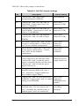
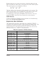
Terms and Abbreviations
Table 1 lists and defines terms and abbreviations that may be used in this
manual.
Table 1. Acronyms
Acronym
Meaning
EPROM
Erasable Programmable Read-Only Memory
EEPROM
Electronically Erasable Programmable Read-Only Memory
NMI
Nonmaskable Interrupt
PIO
Programmable Input/Output Circuit
(Individually Programmable Input/Output)
PRT
Programmable Reload Timer
RAM
Random Access Memory
RTC
Real-Time Clock
SIB2
Serial Interface Board 2
SRAM
Static Random Access Memory
UART
Universal Asynchronous Receiver Transmitter
Conventions
Table 2 lists and defines typographical conventions that may be used in
this manual.
Table 2. Typographical Conventions
Example
Description
while
Courier font (bold) indicates a program, a fragment of a
program, or a Dynamic C keyword or phrase.
// IN-01…
Program comments are written in Courier font, plain face.
Italics
Indicates that something should be typed instead of the
italicized words (e.g., in place of filename, type a file's
name).
Edit
Sans serif font (bold) signifies a menu or menu selection.
...
An ellipsis indicates that (1) irrelevant program text is
omitted for brevity or that (2) preceding program text may
be repeated indefinitely.
[ ]
Brackets in a C function’s definition or program segment
indicate that the enclosed directive is optional.
< >
Angle brackets occasionally enclose classes of terms.
a | b | c
A vertical bar indicates that a choice should be made from
among the items listed.
viii About This Manual
BL1200
Programming Abbreviations
For convenience, this manual uses the following pseudo types.
• uint means unsigned integer
• ulong means unsigned long
These pseudo types are not standard C keywords; therefore, they will not
function in an application unless first declared with typedef or
#define.
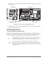
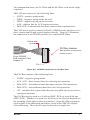
A black square indicates
pin 1 of all headers.
Pin 1
J1
Pin Number 1
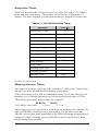
Measurements
All diagram and graphic measurements are in inches followed by millimeters enclosed in parenthesis.
Icons
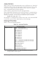
Table 3 displays and defines icons that may be used in this manual.
Table 3. Icons
Icon
Meaning
Refer to or see
Please contact
Caution
Note
High Voltage
Tip
FD
BL1200
Tip
Factory Default
About This Manual ix
x About This Manual
BL1200
CHAPTER 1:
OVERVIEW
Chapter 1 provides an overview and a brief description of the BL1200
features.
BL1200
Overview 11
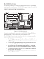
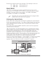
BL1200 Overview
The BL1200 controller is extremely compact and is capable of handling
small control jobs at low cost. The BL1200’s rugged design allows it to be
used in the harshest industrial environments.
Figure 1-1 illustrates the BL1200 board layout.
Watchdog Timer
J3
J4
U3
U1
X0
U4
EPROM
J5
Z180
J10
U11
EEPROM
U2
P1
U5
U6
RAM
U18
J2
J8
U14
L1
C3
U15
J11
RS485
U9
Real-Time Clock
Reset Button
LED
PAL
J6
Crystal
U12
PIO
U16
RS485
U13
Power Optical Isolator Optical Isolator
Driver
Driver
Relay Driver
U19
GND0
U10
J14
J1
H3 (Optically Isolated
Inputs)
H2 (Power,
Serial Ports)
H1 (Relay-Driver
Outputs)
Figure 1-1. BL1200 Controller
Expansion boards may be connected to the BL1200’s 26-pin PLCBus to
handle moderate or large control jobs, all at moderate cost.
The BL1200 differs in several ways from other low-cost programmablelogic controllers widely used in industry:
• The BL1200 is programmed in C, a well-known “high-level
language.” This saves having to learn other coding schemes, such
as ladder logic.
• The BL1200’s open-board design costs less and provides more
mounting flexibility than closed-frame designs.
• A variety of low-cost expansion boards made by Z-World and
others allows the BL1200 to accommodate increased demands.
• The open architecture of the BL1200’s expansion bus makes it
easy to design add-on boards.
• The BL1200’s two RS-485 serial ports allow it to communicate
easily with other devices.
12 Overview
BL1200
Features
The BL1200 has eight optically isolated inputs, eight relay-driver outputs,
and two half-duplex RS-485 serial communication ports. Other standard
features are battery-backed RAM, a battery-backed real-time clock, two
counters, and a switching power supply. These subsystems allow considerable flexibility to read inputs from switches and sensors, and to control
output devices such as high-voltage or low-voltage relays.
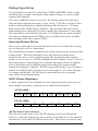
Optically Isolated Inputs
The BL1200’s inputs incorporate NEC 2506-4 optical isolators, as shown
in Figure 1-2. The optical isolator includes two LEDs whose polarities are
reversed to enable the inputs to accept current flowing in either direction.
The inputs even accept alternating current with the help of software that
can detect a pulsing signal.
+5 V
10 kΩ
Input
to PIO
Common
4.3 kΩ
Figure 1-2. BL1200’s Optically Isolated Inputs
The standard 4.3 kΩ load resistor accommodates input voltages of
3 V to 40 V, which is well suited for detecting contact closures.
The BL1200 is protected from external voltage transients because the
internal logic circuits are isolated from the inputs. An input outside the
specified voltage range would likely damage either the load resistor or the
optical isolator chip. Both are easily replaced.
Relay-Driver Outputs
Each of the BL1200’s eight relay-driver outputs can sink a DC current of
approximately 300 mA at about 50 V. Each output includes a protective
diode, allowing it to drive an inductive load such as a relay coil or a small
solenoid.
Serial Ports
The BL1200 has two RS-485 ports that allow serial data to be sent over a pair
of twisted wires up to several kilometers at rates as high as 57,600 bps.
BL1200
Overview 13
A number of BL1200 boards can be connected together on the same
twisted pair, and this same wire pair may be shared with other devices,
such as a PC.
When several devices share an RS-485 bus, one device acts as master and
the others serve as slaves. If a standard 2-wire RS-485 bus is augmented
with two additional wires providing +24 V and ground, the resulting 4-wire
bus can provide power and communications to a network of BL1200s
distributed throughout a building or factory.
Battery-Backed Clock
The BL1200’s time/date clock, accurate to approximately 1 second per
day, can be used to sequence events or to record a history of events. A
small onboard lithium battery powers the clock whenever external power
shuts off. Under normal operating conditions, this battery can power the
clock for approximately 10 years.
Switching Power Supply
The BL1200’s built-in switching power supply accepts unregulated DC
input of 9 V to 35 V. This power supply conserves energy, making the
BL1200 suitable for many battery-powered applications.
Expansion Bus
A 26-pin PLCBus connector along one edge of the BL1200 provides two
buses in one: an LCD interface bus, and the PLC expansion bus.
Various LCDs and keypad units can be used with the BL1200 through this
connector.
Z-World provides several expansion boards that connect directly to the
BL1200 on this bus. You can create an extended system using a Z-World
controller and one or more expansion cards. The cards communicate over
the PLC bus and function as a single system. User-designed expansion
boards can also connect to the BL1200.
See Appendix D for more information on expansion boards.
Appendix E provides details on the PLCBus.
Memory
Memory for running programs on the BL1200 is provided by a batterybacked, static RAM chip and an EPROM. Memory chips from 32K to
512K are supported.
Another, much smaller, nonvolatile block of memory on the BL1200 is
implemented with an EEPROM. The EEPROM’s 512-byte capacity stores
semipermanent information, such as bus addresses for the RS-485 communications ports or calibration constants. The upper half of the EEPROM
can be write protected.
14 Overview
BL1200
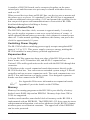
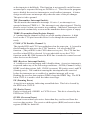
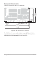
DIN Rail
The BL1200 and its expansion boards can be mounted using plastic standoffs to any flat surface that accepts screws. BL1200s can also be mounted
in modular circuit-board holders and attached to DIN rail, a mounting
system widely used for electrical components and controllers, as shown in
Figure 1-3.
Bus Connectors
BL1200
Modular PC
Board Holders
Expansion Cards
DIN Rail
Figure 1-3. Mounting BL1200 on DIN Rail
A DIN rail is a long metal rail. The BL1200 and other add-on boards slide
snugly into modular, plastic printed-circuit board holders, which then snap
onto the rail.
The circuit holders, 75 mm wide, are available in multiples of lengths of
11.25 mm, 22.5 mm, or 45 mm. These holders can be snapped end-to-end
to create a tray of almost any length.
Appendix B provides detailed specifications for the BL1200.
BL1200
Overview 15
Software Development and Evaluation Tools
Dynamic C, Z-World’s Windows-based real-time C language development
system, is used to develop software for the BL1200. The host PC downloads the executable code through the BL1200’s RS-485 port to one of the
following places:
• battery-backed RAM, or
• ROM written on a separate ROM programmer and then substituted for the standard Z-World ROM.
This allows fast in-target development and debugging.
A BL1200 Developer’s Kit contains the manual, schematics, programming
cable, power supply, 128K SRAM, RS-232 to RS-485 converter, and a
Demonstration Board to simulate input/output.
Z-World’s Dynamic C reference manuals provide complete
software descriptions and programming instructions.
Typical Applications
Machine Control
Many small machines are controlled using contact-closure inputs and
solenoid outputs. The BL1200’s optically isolated input channels can
receive mechanical contact closures and pushbutton signals from a human
operator. Its outputs can operate solenoid valves and small actuators. AC
devices can be switched on and off by adding an expansion board containing relays, such as Z-World’s XP8400 board, or by driving a relay with the
BL1200’s high-current outputs. The high-current outputs can also operate
solid-state relay modules that switch 120 V or 240 V AC.
Distributed Control
In certain types of factory control, and in many manufacturing tests, control must be provided at different locations throughout a building, with
centralized control from a single location. A number of BL1200s can be
networked together with an RS-485 communication bus to solve this type
of problem.
For example, several BL1200s can be used to control several separate
pieces of equipment that test finished products. Each test station, running
autonomously, periodically sends statistics to a central station. Software is
downloaded to the distributed stations over the serial network.
As another example, a network of up to 256 BL1200s is used for a distributed building-access control system. Each BL1200 controls its buildingentry site. Each BL1200 reports to, and is controlled by, a central station.
16 Overview
BL1200
CHAPTER 2:
GETTING STARTED
Chapter 2 provides instructions for connecting the BL1200 to a host PC
and running a sample program.
BL1200
Getting Started 17
Initial BL1200 Setup
Parts Required
•
24 V unregulated DC power supply
•
Programming cable
•
RS-485 to RS-232 converter or XP8700 expansion board.
The necessary parts are supplied with the developer’s kit.
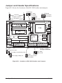
Connecting the BL1200 to a Host PC
1. Connect the power supply to the BL1200.
The BL1200 normally operates from a 24 V unregulated DC power
supply, but will operate satisfactorily with a 12 V unregulated power
supply. However, if the BL1200 is to be connected to one or more
accessory boards that include 24 V relays, the 12 V supply will not
operate the 24 V relays. The 24 V DC wall transformer provided in
Z-World’s Developer’s Kit is recommended.
Connect the two leads from the DC power supply or wall transformer
to sockets 1 and 2 on header H2, as shown in Figure 2-1. Use a small
screwdriver to push down the small plastic lever above the socket to
insert a lead into one of the connection sockets. Do not power up the
power supply until the remaining steps have been completed.
10
1
H3
8
1
H2
10
1
H1
+24V
GND
Figure 2-1. Bl1200 Power Supply Connections at Header H2
Be careful to connect the power supply wires to the correct
sockets on header H2. The BL1200 may be destroyed in an
instant if the power supply is connected to the wrong socket.
A protective diode prevents damage to the BL1200 if the
power supply polarity is reversed.
18 Getting Started
BL1200
2. Check jumpers.
Ten jumpers on the BL1200 board define the hardware configuration.
Appendix B lists the jumper settings.
3. Establish a serial communications link.
A PC “communicates” with the BL1200 via Serial Port 0 on the
BL1200’s microprocessor using RS-485 communications protocols.
There are two options to install the communications link:
Option 1—RS-232 to RS-485 converter. This option with the
developer’s kit is more expensive than the XP8700 communication
board, but provides all the necessary programming accessories.
Use the serial cable to connect the PC’s 9-pin or 25-pin RS-232 serial
port to a Z-World RS-232 to RS-485 converter. Either PC serial port
(COM1 or COM2) may be used. Then connect four wires between the
converter and the BL1200 as shown in Figure 2-2.
9-pin to 25-pin
adapter
(optional)
9-pin serial
connector
serial cable
485+
485
RS-232 to
RS-485
converter
BL1200
to PC
GND
+5 V
4850+
+24 V
GND
4850-
Figure 2-2. Using Converter to Program BL1200
BL1200
Getting Started 19
Figure 2-3 shows a detailed view of the link between the converter and
the BL1200. Two short, insulated wires link sockets 3 and 4 on the
converter and sockets 3 and 4 on header H2 of the BL1200, respectively. These are the two RS-485 channels. The other two wires, for
ground and +5 V, link sockets 7 and 8 on the converter and sockets 7
and 8 on header H2, respectively, as shown.
8
1
Converter
GND
+5 V
10
485
485+
1
H3
8
1
H2
10
1
H1
+24V
GND
Figure 2-3. Detail View of RS-232 to RS-485 Converter Connections
Option 2—XP8700 RS-232 communication board. This option is less
expensive, but lacks the accessories provided with the Developer’s Kit.
Use the serial cable to connect the PC’s 9-pin or 25-pin RS-232 serial
port to the XP8700. Either PC serial port (COM1 or COM2) may be
used. The serial cable may be connected to the RJ-12 jack or to the
header on the XP8700, depending on the plug on the serial cable.
20 Getting Started
BL1200
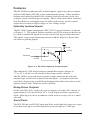
The XP8700 is then connected to the BL1200’s PLCBus port, as shown
in Figure 2-4.
BL1200
GND0
U6
J3
U1
PAL
Z180
J10
U11
EEPROM
U2
U1
1
3.686
MHz
P2
U5
P1
Latch
RN1
U5
U2
RS-232 Driver
C3
C4
R1
R2 D1 D2
C2
U6
RAM
U18
SCC2691 UART
C1
J5
PAL
J6
PAL
X0
U4
EPROM
U4
P1
J4
U3
U14
L1
C3
U15
J2
J8
J11
RS485
U9
Real-Time Clock
U12
PIO
U16
H1
RS-232
Jack
RS485
U13
Power Optical Isolator Optical Isolator
Driver
Driver
Relay Driver
XP8700
U10
J14
J1
J1
H2
H3 (Optically Isolated
Inputs)
Bus Connector
to serial cable
H2 (Power,
Serial Ports)
H1 (Relay-Driver
Outputs)
+24 V
RJ12 Connector
to serial cable
GND
Figure 2-4. Use of 8700 to Program BL1200
4. The BL1200 is now ready for programming. The power supply may be
plugged in and turned on.
Running Dynamic C
Test the Communication Line
Double-click the Dynamic C icon to start the software. Note that the PC
attempts to communicate with the BL1200 each time Dynamic C is started.
No error messages are displayed once communication is established.
BL1200
See Appendix A, Troubleshooting, if an error message such as
Target Not Responding or Communication Error appears.
Once the necessary changes have been made to establish
communication between the host PC and the BL1200, use the
Dynamic C shortcut <Ctrl-Y> to reset the controller and initiate
communication.
Getting Started 21
Selecting Communications Rate, Port, and Protocol
The communication rate, port, and protocol are all selected by choosing
Serial Options from Dynamic C’s OPTIONS menu.
The BL1200’s default communication rate is 19,200 baud. However, the
Dynamic C software shipped by Z-World may be initialized for a different
rate. To begin, adjust the communications rate to 19,200 baud.
Make sure that the PC serial port used to connect the serial cable (COM1
or COM2) is the one selected in the Dynamic C OPTIONS menu. Select
the 1-stop-bit protocol.
Running a Sample Program
As a final test of the communications link, run the sample program
PFLASH.C in the Dynamic C SAMPLES directory. This program flashes the
LED that sits adjacent to the Z180 chip on the BL1200 board.
Prior to running this test, be sure to set the communications parameters in
Dynamic C so that the PC and the BL1200 are handshaking properly.
1. Compile the program by pressing F3 or by choosing Compile from the
COMPILE menu. Dynamic C compiles and downloads the program.
2. Run the program by pressing F9 or by choosing Run from the RUN
menu. The LED on the BL1200 will begin flashing continuously.
4. Press <Ctrl-Z> to stop execution of the program.
5. If needed, press F9 to restart execution of the program.
22 Getting Started
BL1200
CHAPTER 3:
BL1200 OPERATION
Chapter 3 describes how to use the BL1200, with a focus on
• how to set the run and programming modes, and
• how to burn a custom program on EPROM.
BL1200
Operation 23
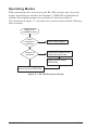
Operating Modes
When starting up after a hard reset, the BL1200 assumes one of several
modes, depending on whether the Dynamic C EPROM is installed and
whether the program jumper across header J1 has been enabled.
The flowchart in Figure 3-1 describes the various actions the BL1200 may
take at startup.
Begin from
hardware reset
Valid
program in
EPROM?
Jumper J1
enabled?
YES
YES
Run user program.
Read input channels for
mode and baud rate.
Write control byte to
EEPROM.
Enter mode specified by
control byte in EEPROM.
Figure 3-1. BL1200 Activity at Startup
24 Operation
BL1200
Run Mode
Once a program has been written and debugged, the program can run from
RAM or an EPROM may be burned.
Before running a program from battery-backed RAM or from a custom
EPROM, first switch the BL1200 from programming mode to run mode.
Reprogram the EEPROM to do this according to the following procedure.
1. Make sure that the BL1200’s power supply is connected properly
at sockets 1 and 2 on header H2, as shown in Figure 3-2.
10
1
H3
8
1
H2
10
1
H1
+24V
GND
Figure 3-2. BL1200 Power Supply Connections at Header H2
2. Connect pins 1 and 2 of header J1 to enable EEPROM reprogramming.
3. Connect a short insulated jumper wire from socket 8 on header
H2 (VCC) to socket 2 on header H3 (COM2).
4. Connect one end of a second short jumper wire to socket 7 on H2
(GND) or socket 10 on header H1 (also GND). Connect the other
end of the wire to socket 7 on header H3 (input channel I4–).
5. Press the reset button. The LED will blink several times, indicating that the new operating mode has been written to the
EEPROM. The BL1200 then begins running continuously.
6 Disconnect the jumper across header J1 and disconnect the wires
connected in Steps 3 and 4.
BL1200
If the Dynamic C EPROM is present on the board, the BL1200
executes the program stored in battery-backed RAM—that is,
the program last run under Dynamic C. If the Dynamic C
EPROM has been replaced with a custom EPROM, then the
BL1200 executes that program.
Operation 25
Returning to Programming Mode
The BL1200 will remain in run mode until the EEPROM is reprogrammed
again. Do the following to return the board to programming mode.
1. Enable EEPROM reprogramming by connecting pins 1 and 2 of
header J1.
2. Connect a short insulated jumper wire from socket 8 on header
H2 (VCC) to socket 1 on header H3 (COM1).
3. Press the reset button. The LED will blink several times, indicating that the new operating mode has been written to the
EEPROM.
4. Disconnect the jumper from header J1 and disconnect the wire
connected in Step 2.
Changing Baud Rate on the BL1200
Use the following procedure to change the baud rate at which the
BL1200’s RS-485 ports communicate with other devices.
1 Make sure the power supply is properly connected at sockets 1
and 2 on header H2 (see Figure 3-1).
2. Connect pins 1 and 2 on header J1.
3. Connect a short, insulated jumper wire from socket 8 on header
H2 (VCC) to socket 1 on header H3 (COM1, the common line for
input ports I0– through I3–).
4. Connect one end of a second, 4-inch jumper wire to socket 7 on
H2 (GND) or socket 10 on header H1 (also GND).
5. Connect the other end of the 4-inch wire to socket 3 on header H3
(I0–), socket 4 on H3 (I1–), or socket 5 on H3 (I2–) as desired,
selecting a baud rate of 57,600 bps, 28,800 bps, or 9600 bps,
respectively. Leave the wire unconnected to select the default
baud rate of 19,200 bps.
6. With the wires still connected, press the board’s reset button. The
LED on the BL1200 board will blink four times, indicating that
information has been written to the EEPROM.
7. Disconnect the jumper across header J1 and disconnect the wires
connected in Steps 3, 4, and 5.
Remember to reset the serial rate in Dynamic C after changing
the baud rate of the BL1200.
26 Operation
BL1200
EPROM
Programming EPROMs
Dynamic C can be used to create a file for programming an EPROM by
selecting the Compile to File option in the COMPILE menu. The BL1200
must be connected to the PC running Dynamic C during this step because
essential library routines must be uploaded from the Dynamic C EPROM
and linked to the resulting file. The output is a binary file (optionally an
Intel hex format file) that can be used to build an application EPROM.
The application EPROM is then programmed with an EPROM programmer that reads either a binary image or the Intel hex format file. The
resulting application EPROM can then replace the EPROM that came with
the BL1200.
Whenever the Dynamic C EPROM is replaced by a custom EPROM, the
BL1200 ignores the program in battery-backed RAM in favor of the
program stored in EPROM.
Choosing EPROMs
Socket U2 can accommodate several different types of EPROMs, including the following.
27C256
27C512
27C010
32K
64K
128K
28 pins
28 pins
32 pins
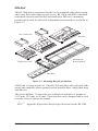
When using a 28-pin EPROM, four pin positions at one end of the socket
are left empty, as shown In Figure 3-3.
U1
J3
J4
U1
U1
PAL
28-pin
EPROM
32-pin
EPROM
J4
PAL
J3
U2
U2
SRAM
U6
J2
SRAM
U6
J2
Figure 3-3. Placement of 28-pin and 32-pin EPROMs on BL1200
BL1200
Remember to set jumpers J2, J3, and J4 on the BL1200 board
according to the settings in Appendix B to indicate the sizes of
EPROM and SRAM chips installed.
Operation 27
Copyrights
The Dynamic C library is copyrighted. Place a label containing the
following copyright notice on the EPROM whenever an EPROM that
contains portions of the Dynamic C library is created.
©1992 Z-World, Inc.
Your own copyright notice may also be included on the label to protect
your portion of the code.
Z-World grants purchasers of the Dynamic C software and the copyrighted
the BL1200 EPROM permission to copy portions of the EPROM library
as described above, provided that:
1 The resulting EPROMs are used only with the BL1200 controllers manufactured by Z-World, Inc., and
2. Z-World’s copyright notice is placed on all copies of the EPROM.
Downloading Programs from a Distance
In some circumstances, there may be a need to download a program to a
BL1200 located some distance away. This is accomplished via a serial
communications link.
Downloading code under these circumstances requires a “monitor”
program on the BL1200. Once written, this program is burned into
EPROM. It then serves as master controller, loading and executing
programs and receiving control when the executed program relinquishes
control.
A properly written monitor program gains control whenever the remote
BL1200 is reset either by power-on, by timeout of a watchdog timer, or by
the reset key. To ensure that the controller sending the downloaded code
can reset a remotely located BL1200, install an external hardware reset
line via one of the remote BL1200’s RS-485 ports (CTS or RXC). Connect the output of the RS-485 receiver to the same reset line as the
BL1200’s onboard reset pushbutton switch.
The BL1200’s memory map and the format for downloaded
files must be correct in a successful monitor program that can
load software files. Both topics are reviewed in Z-World’s
Dynamic C Technical Reference manual.
28 Operation
BL1200
CHAPTER 4:
SYSTEM DEVELOPMENT
Chapter 4 provides the following information to develop the BL1200 for
specific uses.
• Optically Isolated Input
• Relay-Driver Output
• Intermittent Operation
• Onboard LED
• Power-Conserving Configuration
• Serial Ports
• Watchdog Timer
• References
BL1200
System Development 29
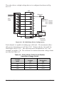
Optically Isolated Input
The BL1200 board has eight optically isolated input channels. Channels
I0– through I3– in Figure 4-1 share a single common line (COM1);
channels I4– through I7– share a second common line (COM2).
H3
10
I7
I6 I4 I2 I0
I6 I3 I1
H2
1
8
H1
1 10
1
COM1 for I0I3
COM2 for I4I7
Figure 4-1. BL1200 Optically Isolated Input Channels
The circuit diagram in Figure 4-2 shows a typical optically isolated input.
+5 V
10 kΩ
Input
to PIO
Common
4.3 kΩ
Figure 4-2. Typical BL1200 Optically Isolated Input
When current flows through an input to the common, or vice versa, one of
the LEDs inside the optical isolator chip illuminates a phototransistor.
This causes current to flow through the 10 kΩ pullup resistor, pulling the
PIO chip’s output low. NEC 2506-4 photocouplers are used, although
other devices may be substituted, if desired. A current of 0.2 mA is sufficient to trigger the photocoupler. The current should not exceed 80 mA so
as not to overheat the photocoupler. Normally, such a high current would
not be encountered without first blowing the 0.5 W 4.3 kΩ resistor.
To avoid overheating the resistor, do not apply more than 50 V. The
resistor supplied will accommodate input of 2 V to 50 V at 0.2 mA to
12 mA. The input can be either AC or DC. If AC is used, the output turns
off briefly each time the AC voltage crosses 0 V.
An AC on-off state can be detected by sampling the logic waveform every
few milliseconds.
30 System Development
BL1200
The common line can be either plus or minus. For example, the common
line can be +24 V when contact closures are being monitored, and the
contacts connect the inputs to ground. For TTL logic input, the common
line would be +5 V, and the TTL drivers would then pull the inputs to
ground, sinking 1 mA.
Relay-Driver Output
The BL1200 has eight high-current output ports. These ports, located on
header H1, are well suited for driving relays and solenoids. The ports can
also be used as logic outputs with the addition of a pullup resistor. Figure 4-3 shows the relay-driver outputs.
H3
10
H2
1
8
H1
1 10
GND
K
1
O8 O6 O4 O2
O7 O5
O3 O1
Figure 4-3. BL1200 Relay Driver
Do not connect to or remove wires from the relay-driver output
ports with a relay (or solenoid) powered up. Doing so can
blow out the driver chip.
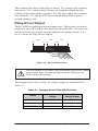
The Sprague driver chip is used. Its voltage ratings are summarized in
Table 4-1.
Table 4-1. Sprague Driver Chip Specifications
Driver
UCN-5841A
BL1200
Breakdown
Voltage
Sustained
Voltage Output
50 V
35 V
UCN-5842A
80 V
50 V
UCN-5843A
100 V
50 V
System Development 31
The relay driver, or high-voltage driver, is configured as shown in Figure 4-4.
H1
1
Serial
Interface
O8
2
O7
3
from
Z180
Solenoid
O6
4
O5
5
O4
6
O3
7
O2
8
O1
9
K
10
Voltage in
Max 35 V 5841A
50 V 5842A
50 V 5843A
Sample
Circuit
+35 V
Power
Supply
GND
Optional
Capacitor
Figure 4-4. BL1200 Relay-Driver Configuration
Each channel is capable of sinking up to 500 mA. The maximum allowable power dissipation is 1.82 W at 25°C. Reduce this by 18.2 mW for
each degree above 25°C. The allowed power dissipation at 70°C, for
example, would be 1 W. The collector-to-emitter saturation voltage limits
are listed in Table 4-2.
Table 4-2. Relay Driver Collector-to-Emitter
Saturation Voltage Limits
Current
(mA)
Collector-Emitter
Voltage
(V)
Power
Dissipation
(W)
100
1.1
0.11
200
1.3
0.26
350
1.6
0.56
32 System Development
BL1200
The output channels are designed to be able to drive inductive loads such
as solenoids or relays. The K line drains the inductive overvoltage. If the
wire connecting K to the power supply is long (inductive), install a filter
capacitor near the board to absorb the voltage surge that occurs when a
device is turned off. If the protective diodes shown in Figure 4-3 are not
connected, inductive loads will blow out the chip.
When driving incandescent lights, take care to protect the relay driver from
overstresses caused by the initial inrush of current.
Software for the Relay Driver
The following routine from the Dynamic C DRIVERS.LIB library allows
writing to the 5841A high-voltage relay-driver chip:
• int hv_wr( char v )
Writes 8 bits to the high-voltage driver. Each bit controls one highvoltage output—a 1 enables (pulls low) the corresponding output,
0 disables the output.
Note that all eight bits are strobed to the output register in one
clock cycle, so all bits change simultaneously. Bit 0 corresponds to output O8, and bit 7 corresponds to output O1. This
routine uses the Z180 CSI/O serial interface to transmit one
character to the relay driver chip.
• int hv_enb()
Enables the 5841 output driver.
• int hv_dis()
Disables the 5841 output driver.
The relay driver is not affected when a hardware reset occurs. In situations
where it is important to disable the relay driver if the system fails, install
an independent turnoff mechanism for equipment controlled by the relaydriver output channels.
If the BL1200’s power supply fails, then the high-voltage driver will be
placed in the OFF state and will remain off when power returns. If the
5841 chip fails because of overstress, it can fail in the ON state, allowing
current to continue to flow. Be sure to consider the consequences of any
such failure and install appropriate protective systems.
BL1200
System Development 33
Intermittent Operation
The BL1200 is equipped with a switching power supply, which enables it
to turn power on and off with software. This is done either under the
control of the time/date clock, or by installing an external switch.
The switching power supply turns off when the signal VOFF is raised high.
It turns on when VOFF is pulled low. A power-on reset lasting approximately 50 milliseconds occurs when the power supply turns on. Computation begins in the program’s main routine approximately 10 milliseconds
after the reset ends.
VOFF can be driven by an external circuit or set permanently in the
enabled (low) state by installing a jumper at header J10. It can also be
controlled by the open-drain output of the 72421 clock chip. The power
supply can be controlled in one of two ways.
1. Install a manual pushbutton that grounds VOFF, enabling the
power supply. The program then calls the library routine powerup
to keep the power supply enabled after the operator releases the
pushbutton. When power is no longer needed, the program calls
the function powerdown, turning the power supply off until
another external event reenables the power supply. This logic can
be used to create a battery-powered instrument that turns off
automatically, conserving the battery, after a certain period of
inactivity.
2. Using the clock, enable power at regular intervals for a short
period of time. The available periods are 1 second, 1 minute, and
1 hour. Pins 2 and 3 of header J8 must be connected; the factory
setting is for pins 3-4 to be connected.
When the power supply is switched on, the power must remain on for at
least 60 ms. As long as the power supply is turned on for only 60 ms of
each second, the power consumption will be decreased by a factor of
approximately 15 to 1. If the power supply is switched on once a minute,
the ratio will be 900 to 1. Powering on once every hour reduces the ratio
to 54,000 to 1.
Now, apply this to a practical situation. If the BL1200 is powered continuously by a 9 V, 500 mA⋅h battery, the board can remain on only 1.5 hours.
With the power enabled only briefly, one time per second, the battery life
can be extended to approximately one day. Powering on briefly once a
minute extends battery life to approximately two months, and powering on
only once an hour extends the battery life to approximately 10 years. This
type of power usage is convenient for applications that involve collection
of data, for example, recording temperature at 1 min intervals. Two library
functions are available for intermittent operation.
34 System Development
BL1200
• setperiodic(int period_code)
Specifies the interval between VOFF pulses from the time-date clock.
A period_code of 4 signifies 1 second, 8 signifies 1 minute, and 12
signifies 1 hour.
• sleep()
Turns power off until next periodic power-on cycle.
The periodic interrupts depend on the mode set into the battery-backed
memory of the time/date clock in the Epson 72421 chip. If a voltage
transient upsets the 72421, or if the board’s lithium battery goes dead, then
the board could fail to wake up at the specified time. To guard against this
kind of failure, add an external wake-up circuit to replace or supplement
the 72421 for critical applications that must run unattended.
Onboard LED
A single LED sits adjacent to the Z180 chip on the BL1200.
The LED turns on (and remains on) whenever the board is powered up. If
an error occurs during startup, the LED flashes one of two continuous
error-message patterns, as explained below.
P attern
M eaning
— · · ·
The board has been set for run m ode, bu t there is no
valid user program in EP R O M or in battery-backed
R AM .
· — · ·
An attem pt w as m ade to write to the EEP R OM with
jum per J11 in write-protect position. (Th is m essage
appears only when initializing EEPR O M .)
The LED also flashes a distinctive verification pattern (four blinks)
whenever one of the parameters in the EEPROM has been changed (see
Appendix D).
The –RTS0 line of Serial Channel 0 controls the onboard LED. The
following function can be used to enable and disable the LED without
disturbing the operation of the serial port.
flasher( int k )
If k is nonzero, the LED is illuminated; if k = 0, the LED is turned off.
BL1200
System Development 35
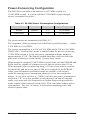
Power-Conserving Configuration
The BL1200 is available with either an 18.432 MHz crystal or a
12.288 MHz crystal. A system with the 12.288 MHz crystal, though
slower, consumes less power.
Table 4-3. BL1200 Power Consumption Configurations
Power Mode
PAL U6
Header J6
Crystal Frequency
Normal
FP0440x
2–3
18.432 MHz
Conserving
FP0445x
1–2
12.288 MHz
The power modes are summarized in Table 4-3.
The frequency of the operating clock is half the crystal frequency — either
9.216 MHz or 6.144 MHz.
The power consumption is 0.8 W at 9.216 MHz and 0.4 W at 6.144 MHz.
If the Z180’s “System Stop” mode is enabled when the power-conserving
12.288 MHz crystal is set up, the power consumption drops further to
approximately 0.2 W. The battery-backed time/date clock can wake the
processor 64 times per second in the “System Stop” mode.
When using the standard 18.4432 MHz crystal, make sure the EPROM and
RAM used are capable of a memory access time no slower than 150 ns.
When using the power-conserving setup, a 150 ns access time is required
for the RAM, and an access time of 200 ns is required for the EPROM.
Other clock frequencies and other setups are possible, with various
tradeoffs among power consumption, memory access time and performance. A very slow clock (e.g., 2 MHz) will decrease power consumption
to about 0.3 W. It is also possible to switch power on and off intermittently or to enter and exit sleep mode or System Stop mode periodically
under control of the battery-backed clock. This can further reduce power
consumption. The cost, of course, is decreased computing power and
slower response time.
36 System Development
BL1200
Serial Ports
The BL1200 has two asynchronous serial ports, shown in Figure 4-5.
These ports, implemented via the Z180’s built-in serial communications
channels, are equipped with half-duplex RS-485 drivers.
10
H3 1
8
H2 1 10 H1
VCC (+5-V output)
+12
1
24 V in
GND
Channel 1 RS-485-
GND for power
Channel 0 RS-485+
Channel 1 RS-485+
Channel 0 RS-485-
Figure 4-5. BL1200 RS-485 Asynchronous Serial Ports
The logical configuration of one of the serial ports appears in Figure 4-6.
enable 485
+5 V
680 Ω
485+
Tx
220 Ω
RS-485 bus
485
Rx
680 Ω
Figure 4-6. Configuration of BL1200 RS-485 Serial Ports
The 680 Ω and 220 Ω resistors are optional. They are needed only on the
two devices located at the ends of an RS-485 twisted-wire pair. When
installed, these resistors terminate and bias the transmission bus, maintaining the line level when no device is driving the bus.
BL1200
System Development 37
The receiver (to Rx) is always enabled. The line “enable 485” enables the
driver (to Tx), which is driven by the PIO on the board. Use the following
function calls to enable and disable the transmitter.
setPIODB(0x80);
// enable
chan 0 driver
resPIODB(0x80);
// disable chan 0 driver
setPIODB(0x40);
// enable
resPIODB(0x40);
// disable chan 1 driver
chan 1 driver
Make sure these calls are used. Do not manipulate the PIO registers
directly. This preserves the relationships among the various PIO inputs
and outputs.
When several devices are connected to an RS-485 twisted pair, one device
is the master device. It sends a command to another device and then
listens for the response from that device. The command contains a device
address. All devices listen, but only the device that recognizes the address
responds.
When the master completes its message, it releases the bus. At some later
time, the slave enables its driver and responds. This delay interval is
known as “turnaround time.” See Figure 4-7.
Master
Turnaround time
Slave
Figure 4-7. Turnaround Time in Master/Slave Communication
If the turnaround time is too short, the master may not have gotten off the
bus before the slave starts to drive the bus. A similar problem can occur
when the slave gets off the bus and the master gets back on the bus to send
the next message. Use a delay interval equal to about three character
transmissions to avoid such problems.
38 System Development
BL1200
Figure 4-8 illustrates how asynchronous data travel after they are transmitted. Every character begins with a start bit and ends with a stop bit. The
start bit has the same polarity as a 0, and the stop bit has the same polarity
as a 1. The 1 state is also the polarity of the line at rest.
485+
Start bit
1
Stop bit
2
4
8
10
20
40
80
485
Figure 4-8. Transmission of Asynchronous Data
(Letter “A” 0x41)
Two special problems can occur when the Z180’s serial ports are used in
half-duplex mode. First, there is no direct way to determine when all the
characters held in the internal transmitter registers have been completely
sent. This happens because the serial port becomes ready for the next
character when the current character is transferred from the transmitter
data register to the transmitter shift register, but there is no way to directly
tell when the transmitter shift register is empty of the last character sent.
When all the characters are sent, the driver must be disabled—but not
before, and not too long after. The best way to determine when a transmission is complete is to make the transmitting station listen to its own
transmission, counting the characters received versus the characters sent.
This is easily done with the BL1200, as the serial port’s receive channel is
always connected to the RS-485 bus.
The second problem involves determining how to time out the turnaround
delay without using a valuable resource such as a timer or a program loop,
which would waste valuable computing time. The receiving device can do
this by sending several 0xff characters with the driver enable off. The
driver can be enabled without sending any spurious data once the start bit
from the last character clears the transmitter shift register. This is because
all the data bits and the stop bit are 1s. The only time delay necessary is a
program loop to time out the length of the start bit after the data register
becomes empty for the last time. This time delay is one-tenth the length of
a full-character time delay. At typical baud rates, it will be of the order of
20 µs to 100 µs.
BL1200
System Development 39
Direct Programming of the Serial Ports
The Z180 technical manuals, listed in the References, provide more
detailed information to help use the serial ports extensively or to use
synchronous communication.
Z-World provides two low-level utility functions to get started:
int sysclock();
int z180baud( int clock, int baud );
The function sysclock returns the clock frequency in units of 1200 Hz,
as read from the EEPROM. (The EEPROM stores the clock frequency at
memory location 108H.)
The function z180baud returns the byte to be stored in CNTLB0/
CNTLB1, considering only the bits needed to set the baud rate. The clock
and baud rates are supplied in units of 1200 Hz. Thus, a 9.216 MHz clock
is expressed by 7680, and 19,200 bps is represented by 16. The function
returns –1 if the baud value cannot be derived from the given clock
frequency.
The serial ports appear to the CPU as a set of registers. Each port can be
accessed directly accessed directly by calling the functions inport and
Table 4-4. Z180 Serial Port UART Registers
Address
Name
Description
00
CNTLA0
Control Register A, Serial Channel 0
01
CNTLA1
Control Register A, Serial Channel 1
02
CNTLB0
Control Register B, Serial Channel 0
03
CNTLB1
Control Register B, Serial Channel 1
04
STAT0
Status Register, Serial Channel 0
05
STAT1
Status Register, Serial Channel 1
06
TDR0
Transmit Data Register, Serial Channel 0
07
TDR1
Transmit Data Register, Serial Channel 1
08
RDR0
Receive Data Register, Serial Channel 0
09
RDR1
Receive Data Register, Serial Channel 1
outport and by using the following symbolic constants in Table 4-4.
For example, to read and write from channel z0, set:
char ch;
ch = inport( RDR0 );
outport( TDR0, ch );
40 System Development
BL1200
Ports may be polled or driven by interrupts. The interrupt vectors are:
0E SER0_VEC
10 SER1_VEC
Z180 Serial Port 0
Z180 Serial Port 1
Baud Rates
The Z180’s serial ports can generate standard baud rates for crystal
frequencies of 6.144 MHz or 9.216 MHz, or a frequency that is a simple
multiple or fraction of these (for example, 3.072 MHz, 4.608 MHz,
6.144 MHz, 9.216 MHz, or 12.288 MHz).
Normally, the crystal on the BL1200 board is stamped with a
number that is twice the clock frequency.
Driving the Serial Ports
Each of the Z180’s independent, full-duplex asynchronous serial channels
has its own baud-rate generator. For either or both channels, the baud rate
can be obtained from an external clock or divided down from the microprocessor clock.
One of the Z180’s internal DMA controllers can be used in conjunction
with the internal serial ports.
The serial ports have an optional multiprocessor communications feature.
When enabled, an extra bit is included in the transmitted character (where
the parity bit would normally go). The receiving Z180s can be programmed to ignore all characters received, except those with the extra
multiprocessing bit enabled. This provides a 1-byte attention message that
can be used to wake up a processor without the processor having to
intelligently monitor all traffic on a shared communications link.
Figure 4-9 shows Serial Channel 0. Serial Channel 1 is similar, but modem
control lines –RTS1 and –DCD0 are not available. Five of the seven
registers shown are directly accessible as internal I/O registers.
Microprocessor Internal Bus
RXA0
RDR0
TDR0
RSR0
TSR0
Shift Register In
RTS0
CTS0
DCD0
CNTLA0
CNTLB0
Baud Rate
Generator
TXA0
Shift Register Out
CLKA0
STAT0
Figure 4-9. BL1200 Serial Channel 0
BL1200
System Development 41
Polling-Type Driver
The polling driver tests the ready flags (TDRE and RDRF) until a ready
condition (for example, transmitter data register empty or receiver data
register full) appears.
If an error condition occurs on receive, the routine must clear the error
flags and take appropriate action, if any. If the –CTS line is used for flow
control, data transmission is halted automatically whenever –CTS goes
high because the TDRE flag is disabled. This prevents the driver from
transmitting more characters because it thinks the transmitter is not ready.
The transmitter will still function with –CTS high, but care must be taken
since the synchronization bit TDRE is not available to properly synchronize loading of the data register (TDR).
Interrupt-Driven Driver
The receiver interrupt for an interrupt-driven driver is enabled for as long
as it is desired to receive characters.
The transmitter interrupt is enabled only while characters are waiting in the
output buffer. When an interrupt occurs, the interrupt routine must
ascertain the cause: receiver data register full, transmitter data register
empty, receiver error, or -DCD0 pin high (Serial Channel 0 only). None of
these interrupts is edge-triggered, so another interrupt will occur immediately if interrupts are re-enabled without disabling the condition that
caused the interrupt. Channel –DCD0 is especially tricky to use because it
cannot be disabled while leaving receive interrupts on. For most designs,
it is suggested that the –DCD0 line be connected directly to ground,
removing it from consideration.
ASCI Status Registers
A status register for each channel provides information about the state of
each channel and allows interrupts to be enabled and disabled.
STAT0 (04H)
7
6
5
4
3
2
1
0
RDRF
OVRN
PE
FE
RIE
/DCD0
TDRE
TIE
R
R
R
R
R/W
R
R
R/W
STAT1 (05H)
7
6
5
4
3
2
1
0
RDRF
OVRN
PE
FE
RIE
CTS1E
TDRE
TIE
R
R
R
R
R/W
R
R
R/W
/DCD0 (Data Carrier Detect)
This bit echoes the state of the /DCD0 input pin for Serial Channel 0.
However, when the input to the pin switches from high to low, the data bit
switches low only after STAT0 has been read. The receiver resets as long
42 System Development
BL1200
as the input pin is held high. This function is not generally useful because
an interrupt is requested as long as /DCD0 is a 1. This forces the programmer to disable the receiver interrupts to avoid endless interrupts. A better
design would cause an interrupt only when the state of the pin changes.
This pin is tied to ground.
TIE (Transmitter Interrupt Enable)
This bit masks the transmitter interrupt. If set to 1, an interrupt is requested whenever TDRE is 1. The interrupt is not edge triggered. This bit
must be set to 0 when you want to stop sending. Otherwise, interrupts will
be requested continuously as soon as the transmitter data register is empty.
TDRE (Transmitter Data Register Empty)
A 1 means that the channel is ready to accept another character. A high
level on the /CTS pin forces this bit to 0 even though the transmitter is
ready.
CTS1E (CTS Enable, Channel 1)
The signals RXS and CTS1 are multiplexed on the same pin. A 1 stored in
this bit makes the pin serve the CTS1 function. A 0 selects the RXS
function. (The pin RXS is the CSIO data receive pin.) The CTS line has
no effect when RXS is selected. It is not advisable to use the CTS1
function on the BL1200 because the RXS line is needed to control several
other devices on the board.
RIE (Receiver Interrupt Enable)
A 1 enables receiver interrupts and 0 disables them. A receiver interrupt is
requested under any of the following conditions: –DCD0 (Channel 0 only),
RDRF (read data register full), OVRN (overrun), PE (parity error), and FE
(framing error). The condition causing the interrupt must be removed
before the interrupts are re-enabled, or another interrupt will occur.
Reading the receiver data register (RDR) clears the RDRF flag. The EFR
bit in CNTLA is used to clear the other error flags.
FE (Framing Error)
A stop bit was missing, indicating scrambled data. This bit is cleared by
the EFR bit in CNTLA.
PE (Parity Error)
Parity is tested only if MOD1 in CNTLA is set. This bit is cleared by the
EFR bit in CNTLA.
OVRN (Overrun Error)
Overrun occurs when bytes arrive faster than they can be read from the
receiver data register. The receiver shift register (RSR) and receiver data
register (RDR) are both full.
BL1200
System Development 43
RDRF (Receiver Data Register Full)
This bit is set when data are transferred from the receiver shift register to
the receiver data register. The bit is set even when one of the error flags is
set, in which case defective data is still loaded to RDR. The bit is cleared
when the receiver data register is read, when the /DCD0 input pin is high,
and by RESET and IOSTOP.
ASCI Control Register A
Control Register A affects various aspects of the asynchronous channel
operation.
CNTLA0 (00H)
7
6
5
4
3
2
1
0
MOD2
MOD1
MOD0
R/W
R/W
R/W
MPE
RE
TE
/RTS0
MPBR/
EFR
R/W
R/W
R/W
R/W
R/W
CNTLA1 (01H)
7
6
5
4
3
2
1
0
MPE
RE
TE
CKA1D
MPBR/
EFR
MOD2
MOD1
MOD0
R/W
R/W
R/W
R/W
R/W
R/W
R/W
R/W
MOD0–MOD2 (Data Format Mode Bits)
MOD0 controls stop bits: 0 ⇒ 1 stop bit, 1 ⇒ 2 stop bits. If 2 stop bits
are expected, then 2 stop bits must be supplied.
MOD1 controls parity: 0 ⇒ parity disabled, 1 ⇒ parity enabled. (See
PEO in control registers B for even/odd parity control.)
MOD2 controls data bits: 0 ⇒ 7 data bits, 1 ⇒ 8 data bits.
MPBR/EFR (Multiprocessor Bit Receive/Error Flag Reset)
Reads and writes on this bit are unrelated. Storing a byte when this bit is 0
clears all the error flags (OVRN, FE, PE). Reading this bit obtains the
value of the MPB bit for the last read operation when multiprocessor mode
is enabled.
/RTS0 (Request to Send, Channel 0)
Store a 1 in this bit to set the RTS0 line from the Z180 high. The output
driver further inverts this line. This bit is essentially a 1-bit output port
without other side effects.
CKA1D (CKA1 Disable)
This bit controls the function assigned to the multiplexed pin (CKA1/–
TEND0): 1 ⇒ –TEND0 (a DMA function) and 0 ⇒ CKA1 (external clock
I/O for Channel 1 serial port).
44 System Development
BL1200
TE (Transmitter Enable)
This bit controls the transmitter: 1 ⇒ transmitter enabled, 0 ⇒ transmitter
disabled. When this bit is cleared, the processor aborts the operation in
progress, but does not disturb TDR or TDRE.
RE (Receiver Enable)
This bit controls the receiver: 1 ⇒ enabled, 0 ⇒ disabled. When this bit is
cleared, the processor aborts the operation in progress, but does not disturb
RDRF or the error flags.
MPE (Multiprocessor Enable)
This bit (1 ⇒ enabled, 0 ⇒ disabled) controls multiprocessor communication mode which uses an extra bit for selective communication when a
number of processors share a common serial bus. This bit has effect only
when MP in control register B is set to 1. When this bit is 1, only bytes
with the MP bit on will be detected. Others are ignored. All bytes
received are processed if this bit is 0. Ignored bytes do not affect the error
flags or RDRF.
ASCI Control Register B
Control Register B for each channel configures multiprocessor mode,
parity and baud rate selection.
CNTLB0 (02H) and CNTLB1 (03H)
7
6
5
4
3
2
1
0
MPBT
MP
/CTS
PS
PEO
DR
SS2
SS1
SS0
R/W
R/W
R/W
R/W
R/W
R/W
R/W
R/W
SS (Source/Speed Select)
Coupled with the prescaler (PS) and the divide ratio (DR), the SS bits
select the source (internal or external clock) and the baud rate divider, as
shown in Table 4-5.
Table 4-5. Baud Rate Divide Ratios
for Source/Speed Select Bits
BL1200
SS2
SS1
SS0
Divide Ratio
0
0
0
÷1
0
0
1
÷2
0
1
0
÷4
0
1
1
÷8
1
0
0
÷ 16
1
0
1
÷ 32
1
1
0
÷ 64
1
1
1
external clock
System Development 45
The prescaler (PS) the divide ratio (DR) and the SS bits form a baud rate
generator (see Figure 4-10).
Processor
Clock
Prescaler
(PS)
÷10
or
÷30
Divide
Ratio
(DR)
Divider
1
2
...
64
External
Clock
16
or
24
Figure 4-10. Baud-Rate Generator
DR (Divide Ratio)
This bit controls one stage of frequency division in the baud rate generator.
If 1 then divide by 64. If 0 then divide by 16. This is the only control bit
that affects the external clock frequency.
PEO (Parity Even/Odd)
This bit affects parity: 0 ⇒ even parity, 1 ⇒ odd parity. It is effective only
if MOD1 is set in CNTLA (parity enabled).
–CTS/PS (Clear to Send/Prescaler)
When read, this bit gives the state of external pin /CTS: 0 ⇒ low,
1 ⇒ high. When /CTS pin is high, RDRF is inhibited so that incoming
receive characters are ignored. When written, this bit has an entirely
different function. If a 0 is written, the baud rate prescaler is set to divide
by 10. If a 1 is written, it is set to divide by 30.
MP (Multiprocessor Mode)
When this bit is set to 1, multiprocessor mode is enabled. The multiprocessor bit (MPB) is included in transmitted data:
start bit, data bits, MPB, stop bits
The MPB is 1 when MPBT is 1 and 0 when MPBT is 0.
MPBT (Multiprocessor Bit Transmit)
This bit controls the multiprocessor bit (MPB). When the MPB is 1,
transmitted bytes will get the attention of other units listening only for
bytes with MPB set.
46 System Development
BL1200
Table 4-6 shows ASCI Control Register B values for baud rates at various
clock frequencies.
Table 4-6. ASCI Control Register B Values for Baud Rates at
Various Clock Frequencies
Clock Frequency (MHz)
Baud
Rate
12.288
76,800
00
38,400
01
9.216
6.144
4,608
3.072
2.304
00
19,200
02
20
01
9600
03
21
02
20
01
4800
04
22
03
21
02
20
2400
05
23
04
22
03
21
1200
06
24
05
23
04
22
600
0D
25
06
24
05
23
300
0E
26
0D
25
06
24
150
2D
0E
26
0D
25
75
2E
2D
0E
26
BL1200
00
System Development 47
Time/Date Clock
The battery-backed time/date clock, also known as the real-time clock or
RTC, uses the Epson 72421 chip.
The 72421A is accurate to approximately one second per day. The
73421B is accurate to approximately five seconds per day. Time is kept to
one second least count and up to 80 years in the future. The lithium
battery should keep the clock going for about 10 years unless the board is
stored at high temperature for long periods with the power off.
An Epson RTC-72421 battery-backed clock appears to the rest of the
controller as 16 I/O registers occupying addresses 050H–05FH. The 16
registers, each four bits wide, appear as the lower four bits of the data byte,
with the upper four bits undefined. Table 4-7 shows how the registers are
arranged.
As can be seen from Table 4-7, the 4-bit registers are mostly binary-coded
decimal (BCD) numbers making up the date and time. The following
notes refer to these registers.
Table 4-7. Epson 72421 Registers
Address
Bit 3
Bit 2
Bit 1
Bit 0
Meaning
Range
050H
051H
052H
053H
054H
055H
056H
057H
058H
059H
05AH
05BH
05CH
S8
D8
S4
S40
M4
M40
H4
AM/PM
D4
M8
M4
S2
S20
M2
M20
H2
H20
D2
D20
M2
Y8
Y80
Y2
Y20
W2
S1
S10
M1
M10
H1
H10
D1
D10
M1
M10
Y1
Y10
W1
Seconds
Tens of secs
Minutes
Tens of mins
Hours
Tens of hrs
Days
Tens of days
Months
Tens of mos
Years
Tens of years
Weekday
0-9
0-5
0-9
0-5
0-9
0-2
0-9
0-3
0-9
0-1
0-9
0-9
0-6
BUSY
HOLD
REG D
MASK
REG E
RSET
REG F
M8
H8
05DH
30
ADJ
Y4
Y40
W4
IRQ
FLG
05EH
T1
T0
05FH
TEST
12/24
48 System Development
INTR/
STND
STOP
BL1200
For 24-hour mode, set the 12/24 bit to 1. Otherwise, the clock runs in 12hour mode and the AM/PM bit will be 1 for PM. When using the 24-hour
mode, mask out the AM/PM bit.
For day of the week, the numbers 0–6 represent Sunday through Saturday.
Leap year is automatically taken into account.
To set the clock for 1990, set year to 90.
Functions to read and write the time/date clock and to change or reset the
time and date are included in the Dynamic C library DRIVERS.LIB.
The following structure is used to hold the date and time:
struct tm{
byte tm_sec;
byte tm_min;
byte tm_hour;
byte tm_mday;
byte tm_mon;
byte tm_year
byte tm_wday;
} tm_val;
//
//
//
//
//
//
//
//
seconds 0-59
minutes 0-59
24 hour time 0-23
day of month 1-31
month 1-12
eg: 90-1990, 101-2001
day of week 0-6
Sunday is 0
Time can also be expressed as seconds since January 1, 1980 (midnight
December 31, 1979).
It takes approximately 600 µs to read the clock chip. The following
functions are provided for reading the time/date clock.
• int tm_rd( struct tm *t )
Reads the time/date clock and returns zero if no error occurs. Returns
-1 if the clock is not working or is not installed.
• long clock()
Reads the 72421 timer and returns time as seconds since January 1,
1980.
The sample program PLCLK.C illustrates a keyboard interface to
display and set the time/date clock manually. The following function
allows the clock to be set from within a program.
• int tm_wr(struct tm *t)
Writes the content of the structure to the clock. Returns 0 if structure is
written normally. Returns –1 if the clock is failing or is not installed.
BL1200
System Development 49
The following functions allow seconds from January 1, 1980 to be
converted to the time structure.
• ulong mktime( struct tm *t )
Converts time expressed as the structure *t into time expressed as
seconds since January 1, 1980. Does not access the timer chip.
• int mktm( struct tm *t, ulong time )
Converts time expressed as seconds (time) into time expressed as the
structure *t. Does not access the timer chip.
50 System Development
BL1200
Watchdog Timer
The watchdog timer is a reliability feature. If the two pins on header J14
are connected, enabling the watchdog, a timer starts running. This timer
must be reset frequently by calling the library function hitwd.
If the watchdog timer runs for 1.6 seconds without being “hit,” it is
considered to have timed out. The BL1200 is then forced into a hardwarereset condition for 50 ms. Once the hardware resets, the board resumes
operation as if the power had just been turned on.
Several Dynamic C library functions allow a power-on reset to be distinguished from a watchdog reset.
The following functions are associated with the watchdog timer.
• void hitwd(void)
Each time this function is called it hits the watchdog timer, postponing
an automatic hardware reset for another 1.6 seconds.
• int wderror(void)
Returns 0 if the previous hardware reset was caused by power on or by
pushing the reset button. Returns a nonzero value if the previous reset
was caused by timeout of the watchdog timer.
Using the Watchdog Timer
The watchdog is “hit” frequently when a Dynamic C program is being
debugged. However, if a jumper is connected across header J14 and a
program that contains no watchdog hits starts running, a reset will take
place after 1.6 seconds, and Dynamic C will report a loss of communications.
The watchdog timer’s purpose is to enable recovery from a fault condition,
such an endless loop or invalid microprocessor state.
Such a fault condition can be caused by an electrical transient or by a software bug. An electrical transient can generate a state internal to the microprocessor that would be impossible during normal operation. A transient
strong enough to upset the state of the microprocessor or erase part of the
memory can be much weaker than that needed to cause permanent damage,
so having the ability to recover from such faults improves the system’s
reliability under stressful environmental conditions.
BL1200
Be especially careful to avoid creating a state in which hitwd
is called repeatedly in an endless loop. The watchdog then
will not time out when it should.
System Development 51
Software bugs that occur only once a week or once a year and cause the
program to enter an endless loop are not unusual. They are difficult to
correct. The following three examples illustrate such bugs.
1. The stack overflows following a coincidence of events such as an
interrupt that occurs when a seldom-executed, but deeply nested
piece of code is executing. If the seldom-executed code is
executed for only 10 ms every five minutes, and if the interrupts
take place only once per hour, on average, then the program will
crash only once or twice per year of continuous operation.
2. A multibyte variable is shared between a high-level and an
interrupt routine. Precautions are not taken to prevent the
occurrence of interrupts while the high-level function is modifying the multibyte variable. Thus the storage of data in the
multibyte variable could be interrupted after only one of two
bytes have been stored, causing the interrupt routine “see” a
mixture of two numbers, the old and new, that is, garbage. If one
of the incorrectly set variables represents an address to jump to,
then the program can crash. The shared keyword provided in
Dynamic C can be used to prevent this type of situation.
3. Hardware and software can interact. Suppose, for example, that a
function processes an A/D conversion value that should always be
positive. If an electrical transient occurs because of the startup of
a nearby motor (which happens, let’s say, only once a day), then
the value of the A/D conversion may go negative and the program
may enter an endless loop. Once again, the programmer has erred
by not anticipating a negative value. It is unlikely the error would
be found through testing.
52 System Development
BL1200
References
Z-World Technical Manuals
Z-World technical manuals are available from Z-World Inc., Davis,
California.
Dynamic C Technical Reference manual. A detailed description of
Dynamic C with some instructions on use.
Z485 Coprocessor Instruction Manual. Detailed information about
installation and use of Z-World’s Z485 communications co-processor
board for IBM PCs.
Zilog Technical Manuals
Zilog technical manuals may be ordered from Zilog, Inc., Campbell,
California.
Z80 PIO Technical Manual. Describes in detail the parallel port used on
the BL1200. Item no. 03-0008-01.
Z80 CTC Technical Manual. More information on the counter-timers
used on the BL1200. Item no. 03-0036-02.
Z80 SIO Technical Manual. Describes the SIO serial port of the BL1200.
A necessity for most SIO programming, especially synchronous modes.
Item no. 03-3033-01.
Z80 Assembly Language Programming. A good reference on assembly
language. Item no. 03-0002-02 (out of print).
Z180 CPU Technical Manual. Description of Z180 processor and
internal peripherals.
When interfacing the Z180 with Z80-style peripherals, consult also the
Z80 CPU Technical Manual, Item no. 03-0029-01, and the Z80 CPU
Programming Manual, Item no. 03-0012-03.
Hitachi Technical Manuals
Order from Hitachi America Ltd., San Jose, California.
HD64180 8-Bit Microprocessor Manual. Covers the HD64180Z, which
is functionally identical to the Zilog Z180 chip used in the BL1200. Item
no. U77.
BL1200
System Development 53
HD64180 8-Bit Microprocessor Programming Manual. Contains a
detailed description of each operation code. Item no. U92.
Specifications for Various Integrated Circuits
Specifications—5841A high-current/high-voltage driver. Sprague Electric
Company, Worcester, Mass., tel. (508) 853-5000.
Specifications—24C04 EEPROM. Microchip, Inc., Chandler, Ariz., tel.
(602) 963-7373. (Note: Xicor of Milpitas, Calif., tel. (408) 432-8888, has
similar parts, and parts of larger capacity.)
54 System Development
BL1200
APPENDIX A:
TROUBLESHOOTING
Appendix A provides procedures for troubleshooting system hardware and
software.
BL1200
Troubleshooting 55
Out of the Box
Check the items listed below before starting development. Rechecking
may help to solve problems found during development.
•
Verify that the BL1200 runs in standalone mode before connecting any
expansion boards or I/O devices.
•
Verify that the entire system has good, low-impedance, separate
grounds for analog and digital signals. The BL1200 is often connected
between the host PC and another device. Any differences in ground
potential can cause serious problems that are hard to diagnose.
•
Do not connect analog ground to digital ground anywhere.
•
Verify that the host PC’s COM port works by connecting a known-good
serial device to the COM port. Remember that a PC’s COM1/COM3
and COM2/COM4 share interrupts. User shells and mouse software, in
particular, often interfere with proper COM-port operation. For example, a mouse running on COM1 can preclude running Dynamic C on
COM3.
•
Use the Z-World power supply supplied with the Developer’s Kit. If
another power supply must be used, verify that it has enough capacity
and filtering to support the BL1200.
•
Use the Z-World cables supplied. The most common fault of other
cables is their failure to properly assert CTS at the RS-485 port of the
BL1200. Without CTS being asserted, the BL1200’s RS-485 port will
not transmit. Assert CTS by either connecting the RTS signal of the
PC’s COM port or looping back the BL1200’s RTS. Check the
connections carefully to the converter or the XP8700 card.
Note that telephone-company wiring has four wires with 4-pin
RJ-11 connectors, whereas the RJ-12 connector has six pins.
56 Troubleshooting
BL1200
Dynamic C Will Not Start
If Dynamic C will not start, an error message on the Dynamic C screen (for
example, Target Not Responding or Communication Error), announces
a communication failure:
•
Wrong Baud Rate — Either Dynamic C’s baud rate is not set correctly
or the BL1200’s baud rate is not set correctly. Both baud rates must be
identical. The BL1200 baud rate is stored in the EEPROM. Chapter 2
described how to change this rate. Dynamic C’s baud rate is set by the
Setup Target command in the SETUP menu.
•
Wrong System Clock Speed in EEPROM —The EEPROM stores the
system clock speed as a word at location 0x108 in multiples of
1200 Hz. If this number is incorrect, the BL1200 will try to communicate at the wrong baud rate.
•
Wrong Communication Mode — Both the PC and the BL1200 must be
using the same protocol: RS-232 (EIA) or RS-485. The BL1200
always uses half-duplex RS-485. Use Dynamic C’s SETUP menu to
check and alter the protocol for the PC.
•
Wrong COM Port — A PC generally has two serial ports, COM1 and
COM2. Specify the one used in the Dynamic C Target Setup menu.
Use trial and error, if necessary.
•
Wrong Port on BL1200 — The BL1200 has two RS-485 serial ports.
Serial Port 0 must be used for the PC interface, as described in Chapter 2.
•
Wrong Operating Mode — Communication with Dynamic C is lost
when the BL1200 is in run mode. Check header J1 and the connections
on header H3 as described in Chapter 2 so that the BL1200 communicates with Dynamic C at 19,200 bps.
•
Wrong Jumper Setting — Check headers J1, J5, and J6 since they affect
the operating mode and the baud rate.
•
Wrong Clock Crystal — The baud rates for serial ports 0 and 1 on the
BL1200 vary, depending on the BL1200 clock frequency. If a the
clock frequency is not 9.216 MHz (18.432 MHz crystal) or 6.144 MHz
(12.288 MHz crystal), the adjustment in baud rate to communicate with
external devices will have to be calculated manually.
•
Plug Reversed on RS-232 to RS-485 Converter — The serial link will
be wired incorrectly if the 10-pin connector on the converter’s serial
cable is reversed.
BL1200
Troubleshooting 57
Dynamic C Loses Serial Link
Dynamic C will lose its link if the program disables interrupts for more
than 50 ms. If a communication method is used that is not driven by the
nonmaskable interrupt (NMI), make sure that interrupts are not disabled
for more than 50 ms. This is not a concern if a communication method
driven by NMI is used.
BL1200 Resets Repeatedly
If the watchdog timer is enabled by installing J14, a system reset will occur
every 1.6 seconds if the watchdog timer is not “hit.” Dynamic C “hits” the
timer, but a user program must include a call to uplc_init at the start of
the program to make sure the watchdog timer is hit periodically.
Input/Output Problems
A strobe is needed to move data in PIO modes 0 and 1. The strobe lines
are connected to J12. Use Mode 3 for static input. Mode 1 may appear to
work, but will be erratic because the strobe line floats.
Power-Supply Problems
The input resistor must be changed when input voltages exceeding 28 V
are used.
If the external power supply does not have sufficient capacity, an additional load such as an LED can trigger a power-fail interrupt, initiating a
hardware reset. The reset triggers the load to be turned off, but then the
computer restarts and turns the load back on. The oscillation can be
corrected by increasing the size of the power supply.
Blown-Out 5841 Driver Chip
The 5841 driver chip[ may blow if SUB floats. Protect the chip by installing a filter capacitor in the line connecting K to the power supply if this
wire is long.
If K is not connected, the 5841 chip will blow if an inductive load is connected. The circuit will then be enable, so be sure to plan for this situation.
58 Troubleshooting
BL1200
Common Programming Errors
Table A-1. Ranges of Dynamic C
Function Types
Type
Range
int
–32,768 (–215) to
+32,767 (215 – 1)
long int
−2,147,483,648 (−231) to
+2147483647 (231 – 1)
float
–6.805646 × 1038 to
+6.805646 × 1038
char
0 to 255
• Values for constants or variables out of range.
• Counting up from, or down to, one instead of zero. In the
software world, ordinal series often begin or terminate with zero,
not one.
• Confusing a function’s definition with an instance of its use in a
listing.
• Not ending statements with semicolons.
• Not inserting commas as required in functions’ parameter lists.
• Leaving out an ASCII space character between characters forming
a different legal—but unwanted—operator.
• Confusing similar-looking operators such as && with &, == with
=, // with /, etc.
• Inadvertently inserting ASCII nonprinting characters into a
source-code file.
BL1200
Troubleshooting 59
60 Troubleshooting
BL1200
APPENDIX B:
SPECIFICATIONS
Appendix B provides the dimensions and specifications for the BL1200
controller.
BL1200
Specifications 61
Hardware Dimensions
(72)
2.835
(69)
(3.4)
0.133
2.717
Figure B-1 illustrates the BL1200’s dimensions.
0.187 dia, 4x
0.133
(4.7)
(3.4)
4.197
(107)
4.33
(110)
Figure B-1. BL1200 Dimensions (in inches)
The BL1200 and its expansion boards fit in standard PC board holders
designed to be mounted on a 35 mm DIN rail. The BL1200 may also be
mounted with screws and standoffs on any flat surface.
62 Specifications
BL1200
Table B-1 presents the specifications for the BL1200 series of controllers.
Table B-1. BL1200 Specifications
Parameter
Board Size
Operating Temperature
Humidity
Input Voltage and Current
Power Consumption
User-Configurable I/O
Digital Inputs
Digital Outputs
Analog Inputs
Analog Outputs
Resistance Measurement
Input
Processor
Clock Speed
SRAM
EPROM
Flash EPROM
EEPROM
Counters
Serial Ports
Serial Rate
Watchdog/Supervisor
Time/Date Clock
Memory-Backup Battery
Keypad and LCD Display
PLCBus Port
BL1200
Specification
4.33” × 2.835” × 0.85”
(110 mm × 72 mm × 22 mm)
-40–+70°C
5%–95%, noncondensing
9–36 V DC, 66 mA at 24 V,
switching supply
• 0.8 W with 9.216 MHz clock
• 0.4 W with 6.144 MHz clock
N/A
8, optically isolated, ±3 V to ±48 V
• 8 channels, sinking continuously 165 mA
each at 50°C and 48 V DC
• 1 channel, sinking continuously 500 mA at
25°C
No
No
No
Z180
9.216 MHz
32K (supports up to 512K)
32K (supports up to 512K)
No
512 bytes
Software-implementable
2 RS-485 (2-wire)
Up to 57,600 bps
Yes
Yes
Yes, 3-year shelf life,
10-year life in use
Supported through PLCBus
Yes
Specifications 63
Jumper and Header Specifications
Figure B-2 shows the locations of the BL1200 headers and jumpers.
J3 EPROM
32K128K
256K, 512K
J5
standard
J4 EPROM
32K
64K512K
POWER CONFIG
low-power
J3
GND0
U1
J4
U3
X0
U4
EPROM
PAL
U19
J11: EEPROM
write-enable
write-protect
J5
J6
Z180
J10
U11
EEPROM
U2
U18
P1
U5
U6
RAM
J2
C3
U15
RS485
J8
U14
L1
J11
U12
Real-Time Clock
PIO
U16
RS485
U13
U9
Power Optical Isolator Optical Isolator
Driver
Driver
Relay Driver
J6
U10
J14
J1
J8
H3
H2
interrupt 2 on clock
power supply controlled by clock
power supply always on
H1
Enable J1 only to
reprogram EEPROM
32K128K
256K, 512K
enable
J2 RAM
do not connect
J4 WATCHDOG
Figure B-2. Locations of BL1200 Headers and Jumpers
64 Specifications
BL1200
Table B-2 shows the jumper connections.
Table B-2. BL1200 Jumper Settings
No.
Description
Factory Setting
J1
Connect pins 1 and 2 only when
reprogramming the EEPROM.
Not connected
J2
Connect pins 1 and 2 for 32K, 64K, or
128K RAM. Connect pins 2 and 3 for
256K or 512K RAM.
Pins 1 and 2
connected (32K)
J3
Connect pins 1 and 2 for 32K, 64K, or
128K EPROM. Connect pins 2 and 3 for
256K or 512K EPROM.
Pins 1 and 2
connected (32K)
J4
Connect pins 1 and 2 for 32K EPROM.
Connect pins 2 and 3 for 64K or larger
EPROMs.
Pins 1 and 2
connected (32K)
J5
(For RAM) Connect pins 1 and 2 for the
low-power configuration. Connect pins 2
and 3 for the standard configuration.
Pins 2 and 3
connected
(standard)
J6
(For EPROM) Connect pins 1 and 2 for
the low-power configuration. Connect
pins 2 and 3 for the standard
configuration.
Pins 2 and 3
connected
(standard)
J8
Connect pins 1 and 2 so that interrupt 2
Pins 3 and 4
will be triggered on the real-time clock.
connected (power
Connect pins 2 and 3 so that the power
supply always on)
supply is controlled by the real-time clock.
Connect pins 3 and 4 so that the power
supply is always on.
J10
When pins 1 and 2 are connected, a nonmaskable interrupt (NMI) will cause a
reset. (Dynamic C triggers NMIs and
power-failures trigger NMIs.)
J11
Connect pins 1 and 2 to write-protect the
Pins 2 and 3
EEPROM. Connect pins 2 and 3 to enable connected
writing to the EEPROM.
(EEPROM writeenabled
J14
Connect pins 1 and 2 to enable the
watchdog timer. Do not connect pins 2
and 3. Normally the watchdog timer is
disabled (pins 1 and 2 not connected).
BL1200
Not connected
Nothing connected
(watchdog
disabled)
Specifications 65
66 Specifications
BL1200
MEMORY,
I/O MAP AND INTERRUPT VECTORS
APPENDIX C:
Appendix C provides detailed information on memory, provides an I/O
map, and lists the interrupt vectors.
BL1200
Memory, I/O Map and Interrupt Vectors 67
BL1200 Memory
The BL1200’s memory is divided into two segments, corresponding to the
memory chip sockets U1 for EPROM and U2 for SRAM. Both the
EPROM chip and the SRAM chip may have 28 or 32 pins. Devices as
large as 512K (8-bit bytes, 32-pin package) may be installed. The static
RAM is backed up during power-off periods by a lithium battery.
A program is run entirely from battery-backed RAM while it is being
developed. Once the program is burned into EPROM, the battery-backed
RAM is normally used only to store data. Therefore, most applications
should work with 32K (8-bit bytes) RAM when running from EPROM.
Additional RAM, say 128K (8-bit bytes) is required to develop applications. In general, 32K of RAM will allow programs up to 20K (2000 C
statements) to be developed, and 128K of RAM will allow programs as
large as 116K (10,000 C statements) to be developed.
Set headers J2, J3 and J4 to correspond to the sizes of the EPROM and
SRAM chips according to the details in Appendix B.
Registers in the I/O space are accessed by calling the Dynamic C library
functions inport and outport, as in these two lines of sample code.
data_value = inport( CNTLA0 );
outport( CNTLA0, data_value );
The library routines IBIT, ISET and IRES can also be used to set and
clear bits in the I/O registers.
68 Memory, I/O Map and Interrupt Vectors
BL1200
Execution Times
Table C-1 provides the execution times for a BL1200 with a 9.216 MHz
clock and zero wait states. These times reflect the use of Dynamic C’s
library. The time required to read from memory is included, but the time
Table C-1. BL1200 Execution Times
Operation
Time (µs)
DMA copy per byte
0.73
Integer assignment
3.4
Integer add
4.4
Integer multiply
18
Integer divide
90
85
Floating add (typical)
Floating multiply
113
Floating divide
320
Long add
28
Long multiply
97
Long divide
415
Floating square root
849
Floating exponent
2503
Floating cosine
3049
to store a result is not.
Memory-Access Times
Two types of memory cycles must be considered. LIR cycles, which fetch
the op code, have the most critical timing requirement.
Some instruction cycles will be standard memory cycles, the other type of
memory cycle. Standard memory cycles require an access time of 95 ns.
The following memory access times are required.
EPROM
SRAM
9.216 MHz, zero-wait
122 ns
176 ns
These times are very conservative. Problems are unlikely, for example, if a
200 ns EPROM is used instead of one rated at 176 ns. However, the
SRAM’s access time must equal that of the EPROM during program development or when executing code in SRAM, because code executes from
RAM during these periods.
BL1200
Memory, I/O Map and Interrupt Vectors 69
Memory Map
Tables C-2 to C-6 list the symbolic names for all the I/O registers on the
BL1200. These symbolic names are treated as unsigned integer constants.
Table C-2. BL1200 Addresses 00-3F Internal Z180 I/O Registers
Address
Name
Description
00
CNTLA0
Control Register A, Serial Channel 0
01
CNTLA1
Control Register A, Serial Channel 1
02
CNTLB0
Control Register B, Serial Channel 0
03
CNTLB1
Control Register B, Serial Channel 1
04
STAT0
Status Register, Serial Channel 0
05
STAT1
Status Register, Serial Channel 1
06
TDR0
Transmit Data Register, Serial Channel 0
07
TDR1
Transmit Data Register, Serial Channel 1
08
RDR0
Receive Data Register, Serial Channel 0
09
RDR1
Receive Data Register, Serial Channel 1
0A
CNTR
Clocked Serial Control Register
0B
TRDR
Clocked Serial Data Register
0C
TMDR0L
Timer Data Register Channel 0, least
0D
TMDR0H
Timer Data Register Channel 0, most
0E
RLDR0L
Timer Reload Register Channel 0, least
0F
RLDR0H
Timer Reload Register Channel 0, most
10
TCR
Timer Control Register
11–13
—
Reserved
14
TMDR1L
Timer Data Register Channel 1, least
15
TMDR1H
Timer Data Register Channel 1, most
16
RLDR1L
Timer Reload Register Channel 1, least
17
RLDR1H
Timer Reload Register Channel 1, most
18
FRC
Free-Running Counter
19–1F
—
Reserved
20
SAR0L
DMA Source Address Channel 0, least
21
SAR0H
DMA Source Address Channel 0, most
22
SAR0B
DMA Source Address Channel 0, extra bits
23
DAR0L
DMA Destination Address Channel 0, least
24
DAR0H
DMA Destination Address Channel 0, most
25
DAR0B
DMA Destination Address Channel 0, extra bits
26
BCR0L
DMA Byte Count Register Channel 0, least
continued…
70 Memory, I/O Map and Interrupt Vectors
BL1200
Table C-2. BL1200 Addresses 00-3F Internal Z180 I/O Registers
(concluded)
Address
Name
Description
27
BCR0H
DMA Byte Count Register Channel 0, most
28
MAR1L
DMA Memory Address Register Channel 1, least
29
MAR1H
DMA Memory Address Register Channel 1, most
2A
MAR1B
DMA Memory Address Register Channel 1, extra
bits
2B
IAR1L
DMA I/O Address Register Channel 1, least
2C
IAR1H
DMA I/O Address Register Channel 1, most
2D
—
Reserved
2E
BCR1L
DMA Byte Count Register Channel 1, least
2F
BCR1H
DMA Byte Count Register Channel 1, most
30
DSTAT
DMA Status Register
31
DMODE
DMA Mode Register
32
DCNTL
DMA / WAIT Control Register
33
IL
Interrupt Vector Low Register
34
ITC
Interrupt / Trap Control Register
35
—
Reserved
36
RCR
Refresh Control Register
37
—
Reserved
38
CBR
MMU Common Base Register
39
BBR
MMU Bank Base Register
3A
CBAR
MMU Common/ Bank Area Register
3B–3D
—
Reserved
3E
OMCR
Operation Mode Control Register
3F
ICR
I/O Control Register
Table C-3. BL1200 Addresses 40-43 PIO Registers
Address
Name
Description
40
PIODA
PIO Port A Data
41
PIOCA
PIO Port A Control
42
PIODB
PIO Port B Data
43
PIOCB
PIO Port B Control
Table C-4. BL1200 Addresses 80-81 LCD Interface
Address
Name
Description
80
—
LCD control register
81
—
LCD data register
BL1200
Memory, I/O Map and Interrupt Vectors 71
Table C-5. BL1200 Addresses C0-CE Expansion Bus
Address
Name
Description
C0
BUSRD0
Primary bus read address
C2
BUSRD1
Secondary bus read address
C4
BUSSPARE
Spare location
C6
BUSRESET
Read this location to reset the bus
C8
BUSADR0
Write bus address, byte 0
CA
BUSADR1
Write bus address, byte 1
CC
BUSADR2
Write bus address, byte 2
CE
BUSWR
Write bus
0B
BUSEXP
Address of bus expansion register
Table C-6. BL1200 Addresses 100-10F
72421 Real-Time Clock Registers
Address
Bit 3
Bit 2
Bit 1
Bit 0
Meaning
Range
100
S8
S4
S2
S1
Seconds
0-9
101
—
S40
S20
S10
10 seconds
0-5
102
M8
M4
M2
M1
Minutes
0-9
103
—
M40
M20
M10
10 minutes
0-5
104
H8
H4
H2
H1
Hours
0-9
105
—
AM/PM
H20
H10
10 hours
0-2
106
D8
D4
D2
D1
Days
0-9
107
—
—
D20
D10
10 days
0-3
108
M8
M4
M2
M1
Months
0-9
109
—
—
—
M10
10 months
0-1
10A
Y8
Y4
Y2
Y1
Years
0-9
10B
Y80
Y40
Y20
Y10
10 years
0-9
10C
—
W4
W2
W1
week days
0-6
10D
30
ADJ
IRQ
FLG
BUSY
HOLD
Register D
—
10E
T1
T0
INTR/
STND
MASK
Register E
—
10F
TEST
12/24
STOP
RSET
Register F
—
72 Memory, I/O Map and Interrupt Vectors
BL1200
Initialized Memory Locations
Table C-7 lists the constants that are initialized at startup.
Table C-7. Constants Initialized at Setup
CLOCKSPEED
Integer containing the clock speed read in units of
1200 Hz from the EEPROM at startup.
BAUDCODE
Integer containing the baud rate in units of 1200 baud
as read from the EEPROM at startup.
JUMPERS
Byte read from the PIB port of the PIO at startup.
Interrupt Vectors
Table C-8 presents a suggested interrupt vector map. Most of these
interrupt vectors can be altered under software control. The addresses are
given in hex, relative to the start of the interrupt vector page, as determined
by the contents of the I-register. These are the default interrupt vectors set
by the boot code in the Dynamic C EPROM.
Table C-8. Interrupt Vectors for Z180 Internal Devices
Address
Name
Description
0x00
INT1_VEC
Expansion bus attention INT1 vector
0x02
INT2_VEC
INT2 vector. Battery-backed timer interrupt when
jumper J8 is set appropriately.
0x04
PRT0_VEC
PRT Timer Channel 0
0x06
PRT1_VEC
PRT Timer Channel 1
0x08
DMA0_VEC
DMA Channel 0
0x0A
DMA1_VEC
DMA Channel 1
0x0C
CSIO_VEC
Clocked Serial I/O
0x0E
SER0_VEC
Asynchronous Serial Port Channel 0
0x10
SER1_VEC
Asynchronous Serial Port Channel 1
A directive such as the following is used to “vector” an interrupt to a user
function in Dynamic C.
#INT_VEC 0x10 myfunction
This particular statement causes the interrupt at offset 10H (serial port 1 of
the Z180) to invoke the function myfunction(). The function must be
declared with the interrupt keyword.
interrupt myfunction() {
...
}
BL1200
Memory, I/O Map and Interrupt Vectors 73
Nonmaskable Interrupts
Power-Fail Interrupts
The following sequence of events takes place when power fails.
1. The nonmaskable interrupt (NMI) signaling power failure is triggered
whenever the unregulated DC input voltage falls below approximately
8 V (subject to voltage divider R3/R4).
2. The system reset is triggered when the regulated +5 V falls below
4.5 V; the reset remains enabled as the voltage falls further. At this
point, the chip select for the SRAM is forced high (standby mode).
Power for the time/date clock and the SRAM is switched to the lithium
backup battery as the regulated voltage falls below the battery voltage
(approximately 3 V).
The power-fail interrupt must be disabled if an external +5 V
power supply is used (not recommended).
The following sample routine demonstrates how to handle a power-fail
interrupt.
#JUMP_VEC NMI_INT myint
interrupt retn myint(){
body of interrupt routine...
for(;;) if( !powerlo() ) return;
}
Normally, a power-fail interrupt routine will not return. Instead, it will
execute shutdown code and then enter a loop until the +5 V falls low
enough to trigger a reset. However, the voltage might fall low enough in a
brownout situation to trigger the power-fail interrupt but not the reset,
resulting in an endless hangup. The library function powerlo returns 1 if
the voltage level falls below the NMI threshold, otherwise it returns 0.
This routine should be called only from an NMI interrupt routine. If
powerlo detects that the low-voltage condition has reversed itself, then
the power-fail routine can restart execution. If a low, but not fatally low,
voltage persists, then you will have to decide what action to take, if any.
The powerlo routine for the BL1200 depends on a jumper being installed
between J1 pin 1 and J10 pin 1. This allows the /NMI signal to be read by
the input used for the programming header. The dual use of this programming header input can present a problem if the low-voltage condition is
present when the processor comes out of reset. This will not happen normally because the reset lasts for about 50 ms after the +5 V passes the
minimum threshold voltage of about 4.5 V. However, if the voltage fails to
74 Memory, I/O Map and Interrupt Vectors
BL1200
rise from the reset threshold to the power-fail threshold within 50 ms, the
program perceives that the programming jumper was installed since the
/NMI signal is low. To force the programming jumper to be ignored always, the EPROM (FP02311 or latter revision) can be edited to clear bit 0
at location 0xE (15 decimal) in the EPROM. This will cause the programming jumper to be ignored.
A situation similar to brownout occurs if the power supply is overloaded.
Say the load temporarily increases, perhaps when an LED is turned on,
causing the power supply to appear to have failed. The interrupt routine
sheds some of the load by doing a shutdown procedure, causing the powerfail condition to go away. If no action is taken to correct the overload, the
system will oscillate around the power fail. To correct this, use a larger
power supply.
Do not forget the interaction that can occur between the watchdog timer
and the power-fail interrupt. If the watchdog is enabled and a brownout
causes an extended stay in the power-fail interrupt routine, then the
watchdog can time out, causing a system restart.
Even if the power is cut off from the board abruptly, a certain amount of
computing time will remain before the +5 V supply falls below 4.5 V. The
amount of time depends on the size of the capacitors in the power supply.
The standard wall transformer provides about 10 ms. If the power cable is
abruptly removed from the BL1200, then only the capacitors on the board
are available, and the time is reduced to a few hundred microseconds.
These times can vary considerably, depending on the board configuration
and the other loads, if any, drawing from the board’s power supply.
The time interval between detection of a power failure and entry to the
user’s power-fail interrupt routine is approximately 100 µs, or less if
Dynamic C’s nonmaskable interrupt communications are not in use.
It is hard to test power-fail interrupt routines presents because the interrupts are normally disabled. Probably the best test method involves
leaving messages in battery-backed memory to track the execution of the
power-fail routines. If a variable transformer is available to drive the wall
transformer, then brownouts and other types of power-fail conditions can
be easily simulated.
BL1200
Memory, I/O Map and Interrupt Vectors 75
Jump Vectors
Jump vectors are special interrupts that occur in a different way. Instead of
loading the address of the interrupt routine from the interrupt vector, jump
vectors cause a jump directly to the address of the vector, for example,
0x66 nonmaskable power-failure interrupt,
which contains a jump instruction to the interrupt routine.
Since nonmaskable interrupts can be used for Dynamic C communications,
the interrupt vector for power failure is normally stored just in front of the
Dynamic C program. A vector may be stored there by the command
#JUMP_VEC NMI_VEC name
The Dynamic C communication routines relay to this vector when the NMI
is caused by a power failure rather than by a serial interrupt.
Interrupt Priorities
Table C-9 lists the interrupt priorities.
Table C-9. Interrupt Priorities
Interrupt Priorities
(Highest Priority)
(Lowest Priority)
*
Trap (Illegal Instruction)
NMI (Nonmaskable Interrupt)
SIO Channel A*
SIO Channel B*
CTC Channel 0*
CTC Channel 1*
CTC Channel 2*
CTC Channel 3*
PIO Channel A*
PIO Channel B*
INT 1 (expansion bus attention line interrupt)
INT 2 (expansion bus attention line interrupt)
PRT Timer Channel 0
PRT Timer Channel 1
DMA Channel 0
DMA Channel 1
Clocked Serial I/O
Asynchronous Serial Port 0
Asynchronous Serial Port 1
The priority of the SIO, CTC, and PIO interrupts can be altered
through the KIO control register.
76 Memory, I/O Map and Interrupt Vectors
BL1200
APPENDIX D:
BL1200
EEPROM
EEPROM 77
EEPROM Parameters
The onboard EEPROM (electrically erasable, programmable, read-only
memory) is used to store the constants and parameters listed in Table D-1.
The four bytes presently in use determine the operation of the BL1200
board when it starts up.
Table D-1. BL1200 EEPROM Assignments
Address
Bytes
Function
Operating Mode:
00
1
1— programming mode
8— run mode/execute user program in RAM or
EPROM on startup
01
1
Baud rate code (in units of 1200 baud)
100
4
Unit serial number*
108
2
Clock speed (in units of 1200 Hz)
*
not yet implemented
The EEPROM has 512 bytes. The upper 256 bytes can be written to only
when header J11 is enabled (pins 2 and 3 are connected). Connect pins 1
and 2 on J11 to write-protect the EEPROM.
When the EEPROM is first initialized, the baud rate is set to 19,200 bits
per second and the operating mode is set to programming mode. The next
section outlines the procedure to change these parameters.
Operating Mode
In programming mode, the board initializes Serial Port 0 for Dynamic C.
When set for run mode, the board attempts to execute a user-written
program stored in battery-backed RAM or in EPROM.
Baud Rate
The baud rate code determines the serial communication rate at which the
BL1200 attempts to communicate with the PC and Dynamic C.
Clock Speed
The clock speed code is used by the BL1200 to compute parameters
necessary to set the serial port. The clock speed is also used by several
Dynamic C library functions.
The clock operates at half the speed of the BL1200’s crystal.
Thus, if 18.432 (or simply 184) is stamped on the crystal case,
the clock speed is 9.216 MHz.
78 EEPROM
BL1200
EEPROM Channels
With header J1 enabled (that is, its two pins are connected), the BL1200—
when restarted by powering up or by pushing the reset button—reads input
channels I0– through I2– and I4– through I6–. It then writes to the
EEPROM data that determine the mode of operation when the BL1200 is
later restarted without J1 enabled.
Each input channel, if connected to VCC and GND, is interpreted as
follows. Notice that channels I3– and I7– are not used:
I0–
I1–
I2–
I4–
I5–
I6–
Set baud rate to 57,600 bps
Set baud rate to 28,800 bps
Set baud rate to 9,600 bps
Set board for run mode
Initialize EEPROM, clock speed 6.144 MHz
Initialize EEPROM, clock speed 9.216 MHz
Input channels I0–, I1–, and I2– are sockets 3, 4, and 5, respectively, on
the BL1200’s header H3. Input channels I4–, I5–, and I6– are sockets 7, 8,
and 9 on header H3. See Figure D-1.
VCC
VCC
COM1
I0+
I1+
I2+
COM2
I3+
PA0PA3
Optical Isolators
I0
I1
I2
I4+
I3
I5+
I6+
I7+
PA4PA7
Optical Isolators
I4
I5
I6
EEPROM Input Channel
Header H3 Socket
COM1
COM2
I0I1I2I4I5I6-
1
2
3
4
5
7
8
9
I7
Figure D-1. EEPROM Channels
BL1200
EEPROM 79
Note that when channel I4– is disconnected (the default condition), the
board is set for programming mode and Serial Port 0 is initialized for use
with Dynamic C. Similarly, when channels I0– through I2– are all left
disconnected (again, the default condition), the BL1200 sets the communications baud rate to 19,200 bits per second.
Inputs I0– through I3– are connected to COM1 (socket 1 on header H3)
and inputs I4– through I7– are connected to COM2 (socket 2 on header
H3). Any input can be turned on by connecting the appropriate common
(COM1 or COM2) line to +5 V (socket 8 on header H2) and connecting
the input channel to GND (socket 7 on header H2 or socket 10 on header
H1).
Changing Parameters Stored in EEPROM
1 Install jumper across header J1.
2 Connect the desired input channel. For example, to change the baud
rate to 57,600, 28,800 or 9,600, connect I0– or I1– or I2–, respectively.
To switch from programming mode to run mode, connect I4–. To
initialize an EEPROM, connect I5– or I6–. Remember that leaving I4–
disconnected (the default condition) switches the board from run mode
back to programming mode. Likewise, leaving I0–, I1–, and I2– all
disconnected will return the communications rate to the default setting
of 19,200 baud.
3 Press the reset button to restart the BL1200. The LED will blink four
times, indicating that one of the parameters stored in EEPROM has
been rewritten.
4 Disconnect J1 and any setup wires. The BL1200 will automatically use
the new mode or baud rate specified for the next restart. The board
will continue to operate with the new setting until the EEPROM is
changed.
Follow the above procedures to change both the baud rate and the operating mode. First, perform the procedure for one of these parameters, then
repeat the procedure for the other parameter.
Error Messages
The LED next to the Z180 chip may flash a continuous dot-dash pattern if
there is an error in setting up the board. Two patterns are possible.
– · · ·
· – · ·
80 EEPROM
The board is set to run mode, but there is no valid user
program in EPROM or in battery-backed RAM.
An attempt was made to write to the EEPROM with J11 in
write-protect position. (This message appears only when
initializing EEPROM.)
BL1200
Remember that EEPROM addresses above 100 may write-protected by a
jumper across header J11.
Library Routines
The following library routines can be used to read and write the EEPROM:
int ee_rd( int address );
int ee_wr( int address, byte data );
The function ee_rd returns a data value or, if a hardware failure occurred,
–1. The function ee_wr returns –1 if a hardware failure occurred, –2 if an
attempt was made to write to the upper 256 bytes with the protection
jumper (header J11) installed, or 0 to indicate a successful write. A writeprotection violation does not wear out the EEPROM. These routines each
require about 2.5 ms to execute. They are not re-entrant, that is, only one
routine at a time will run.
BL1200
The EEPROM has a rated lifetime of only 10,000 writes (unlimited reads). Do not write the EEPROM from within a loop.
The EEPROM should be written to only in response to a human request for each write.
EEPROM 81
82 EEPROM
BL1200
APPENDIX E:
PLCBUS
Appendix E provides the pin assignments for the PLCBus, describes the
registers, and lists the software drivers.
BL1200
PLCBus 83
PLCBus Overview
The PLCBus is a general-purpose expansion bus for Z-World controllers.
The PLCBus is available on the BL1200, BL1600, BL1700, PK2100, and
PK2200 controllers. The BL1000, BL1100, BL1300, BL1400, and
BL1500 controllers support the XP8300, XP8400, XP8600, and XP8900
expansion boards using the controller’s parallel input/output port. The
BL1400 and BL1500 also support the XP8200 and XP8500 expansion
boards. The ZB4100’s PLCBus supports most expansion boards, except
for the XP8700 and the XP8800. The SE1100 adds expansion capability
to boards with or without a PLCBus interface.
Table E-1 lists Z-World’s expansion devices that are supported on the
PLCBus.
Table E-1. Z-World PLCBus Expansion Devices
Device
Description
EXP-A/D12
Eight channels of 12-bit A/D converters
SE1100
Four SPDT relays for use with all Z-World controllers
XP8100 Series
32 digital inputs/outputs
XP8200
“Universal Input/Output Board”
—16 universal inputs, 6 high-current digital outputs
XP8300
Two high-power SPDT and four high-power SPST relays
XP8400
Eight low-power SPST DIP relays
XP8500
11 channels of 12-bit A/D converters
XP8600
Two channels of 12-bit D/A converters
XP8700
One full-duplex asynchronous RS-232 port
XP8800
One-axis stepper motor control
XP8900
Eight channels of 12-bit D/A converters
Multiple expansion boards may
be linked together and connected to a Z-World controller
to form an extended system.
Figure E-1 shows the pin layout
for the PLCBus connector.
GND
A0X
LCDX
D1X
D3X
D5X
D7X
GND
GND
GND
GND
+24 V
(+5 V) VCC
26
24
22
20
18
16
14
12
10
8
6
4
2
25
23
21
19
17
15
13
11
9
7
5
3
1
VCC (+5 V)
/RDX
/WRX
D0X
D2X
D4X
D6X
A1X
A2X
A3X
strobe /STBX
attention /AT
GND
Figure E-1. PLCBus Pin Diagram
84 PLCBus
BL1200
Two independent buses, the LCD bus and the PLCBus, exist on the single
connector.
The LCD bus consists of the following lines.
•
•
•
•
•
LCDX—positive-going strobe.
/RDX—negative-going strobe for read.
/WRX—negative-going strobe for write.
A0X—address line for LCD register selection.
D0X-D7X—bidirectional data lines (shared with expansion bus).
The LCD bus is used to connect Z-World’s OP6000 series interfaces or to
drive certain small liquid crystal displays directly. Figure E-2 illustrates
the connection of an OP6000 interface to a controller PLCBus.
Yellow wire
on top
PLCBus Header
Note position of connector
relative to pin 1.
From OP6000
KLB Interface Card
Header J2
Pin 1
Figure E-2. OP6000 Connection to PLCBus Port
The PLCBus consists of the following lines.
•
/STBX—negative-going strobe.
•
A1X–A3X—three control lines for selecting bus operation.
•
D0X–D3X—four bidirectional data lines used for 4-bit operations.
•
D4X–D7X—four additional data lines for 8-bit operations.
•
/AT—attention line (open drain) that may be pulled low by any device,
causing an interrupt.
The PLCBus may be used as a 4-bit bus (D0X–D3X) or as an 8-bit bus
(D0X–D7X). Whether it is used as a 4-bit bus or an 8-bit bus depends on
the encoding of the address placed on the bus. Some PLCBus expansion
cards require 4-bit addressing and others (such as the XP8700) require
8-bit addressing. These devices may be mixed on a single bus.
BL1200
PLCBus 85
There are eight registers corresponding to the modes determined by bus
lines A1X, A2X, and A3X. The registers are listed in Table E-2.
Table E-2. PLCBus Registers
Register
Address
A3
A2
A1
Meaning
BUSRD0
C0
0
0
0
Read data, one way
BUSRD1
C2
0
0
1
Read data, another
way
BUSRD2
C4
0
1
0
Spare, or read data
BUSRESET
C6
0
1
1
Read this register to
reset the PLCBus
BUSADR0
C8
1
0
0
First address nibble
or byte
BUSADR1
CA
1
0
1
Second address
nibble or byte
BUSADR2
CC
1
1
0
Third address nibble
or byte
BUSWR
CE
1
1
1
Write data
Writing or reading one of these registers takes care of all the bus details.
Functions are available in Z-World’s software libraries to read from or
write to expansion bus devices.
To communicate with a device on the expansion bus, first select a register
associated with the device. Then read or write from/to the register. The
register is selected by placing its address on the bus. Each device recognizes its own address and latches itself internally.
A typical device has three internal latches corresponding to the three
address bytes. The first is latched when a matching BUSADR0 is detected. The second is latched when the first is latched and a matching
BUSADR1 is detected. The third is latched if the first two are latched and
a matching BUSADR2 is detected. If 4-bit addressing is used, then there
are three 4-bit address nibbles, giving 12-bit addresses. In addition, a
special register address is reserved for address expansion. This address, if
ever used, would provide an additional four bits of addressing when using
the 4-bit convention.
If eight data lines are used, then the addressing possibilities of the bus
become much greater—more than 256 million addresses according to the
conventions established for the bus.
86 PLCBus
BL1200
Place an address on the bus by writing (bytes) to BUSADR0, BUSADR1
and BUSADR2 in succession. Since 4-bit and 8-bit addressing modes
must coexist, the lower four bits of the first address byte (written to
BUSADR0) identify addressing categories, and distinguish 4-bit and 8-bit
modes from each other.
There are 16 address categories, as listed in Table E-3. An “x” indicates
that the address bit may be a “1” or a “0.”
Table E-3. First-Level PLCBus Address Coding
First Byte
Mode
Addresses
Full Address Encoding
–
–
–
–
–
–
–
–
–
–
–
–
–
–
–
–
0
0
0
0
0
0
0
0
0
0
1
1
0
1
0
1
4 bits × 3
256
256
256
256
–
–
–
–
–
–
–
–
–
–
–
–
x
x
x
x
0
0
0
0
1
1
1
1
0
0
1
1
0
1
0
1
5 bits × 3
2,048
2,048
2,048
2,048
– – x x 1 0 0 0
– – x x 1 0 0 1
6 bits × 3
16,384
16,384
– – x x 1 0 1 0
6 bits × 1
4
xx1010
– – – – 1 0 1 1
4 bits × 1
1
1011 (expansion register)
x x x x 1 1 0 0
8 bits × 2
4,096
x x x x 1 1 0 1
8 bits × 3
1M
x x x x 1 1 1 0
8 bits × 1
16
xxxx1110
x x x x 1 1 1 1
8 bits × 1
16
xxxx1111
0000
0001
0010
0011
xxxx
xxxx
xxxx
xxxx
x0100
x0101
x0110
x0111
xxxx
xxxx
xxxx
xxxx
xxxxx
xxxxx
xxxxx
xxxxx
xxxxx
xxxxx
xxxxx
xxxxx
xx1000 xxxxxx xxxxxx
xx1001 xxxxxx xxxxxx
xxxx1100 xxxxxxxx
xxxx1101 xxxxxxxx xxxxxxxx
This scheme uses less than the full addressing space. The mode notation
indicates how many bus address cycles must take place and how many bits
are placed on the bus during each cycle. For example, the 5 × 3 mode
means three bus cycles with five address bits each time to yield 15-bit
addresses, not 24-bit addresses, since the bus uses only the lower five bits
of the three address bytes.
BL1200
PLCBus 87
Z-World provides software drivers that access the PLCBus. To allow
access to bus devices in a multiprocessing environment, the expansion
register and the address registers are shadowed with memory locations
known as shadow registers. The 4-byte shadow registers, which are saved
at predefined memory addresses, are as follows.
SHBUS0
Bus expansion
SHBUS0+1
BUSADR0
SHBUS1
SHBUS0+2
BUSADR1
SHBUS1+1
SHBUS0+3
BUSADR2
Before the new addresses or expansion register values are output to the
bus, their values are stored in the shadow registers. All interrupts that use
the bus save the four shadow registers on the stack. Then, when exiting the
interrupt routine, they restore the shadow registers and output the three
address registers and the expansion registers to the bus. This allows an
interrupt routine to access the bus without disturbing the activity of a
background routine that also accesses the bus.
To work reliably, bus devices must be designed according to the following
rules.
1. The device must not rely on critical timing such as a minimum delay
between two successive register accesses.
2. The device must be capable of being selected and deselected without
adversely affecting the internal operation of the controller.
Allocation of Devices on the Bus
4-Bit Devices
Table E-4 provides the address allocations for the registers of 4-bit
devices.
Table E-4. Allocation of Registers
A1
A2
A3
000j
000j
xxxj
digital output registers, 64 registers
64 × 8 = 512 1-bit registers
000j
001j
xxxj
analog output modules, 64 registers
000j
01xj
xxxj
digital input registers, 128 registers
128 × 4 = 512 input bits
000j
10xj
xxxj
analog input modules, 128 registers
000j
11xj
xxxj
128 spare registers (customer)
001j
xxxj
xxxj
512 spare registers (Z-World)
j
x
88 PLCBus
Meaning
controlled by board jumper
controlled by PAL
BL1200
Digital output devices, such as relay drivers, should be addressed with
three 4-bit addresses followed by a 4-bit data write to the control register.
The control registers are configured as follows
bit 3 bit 2
A2 A1
bit 1
A0
bit 0
D
The three address lines determine which output bit is to be written. The
output is set as either 1 or 0, according to D. If the device exists on the
bus, reading the register drives bit 0 low. Otherwise bit 0 is a 1.
For digital input, each register (BUSRD0) returns four bits. The read
register, BUSRD1, drives bit 0 low if the device exists on the bus.
8-Bit Devices
Z-World’s XP8700 and XP8800 expansion boards use 8-bit addressing.
Refer to the XP8700 and XP8800 manual.
Expansion Bus Software
The expansion bus provides a convenient way to interface Z-World’s
controllers with expansion boards or other specially designed boards. The
expansion bus may be accessed by using input functions. Follow the
suggested protocol. The software drivers are easier to use, but are less
efficient in some cases. Table E-5 lists the libraries.
Table E-5. Dynamic C PLCBus Libraries
Library Needed
Controller
DRIVERS.LIB
All controllers
EZIOTGPL.LIB
BL1000
EZIOLGPL.LIB
BL1100
EZIOMGPL.LIB
BL1400, BL1500
EZIOPLC.LIB
BL1200, BL1600, PK2100, PK2200, ZB4100
EZIOPLC2.LIB
BL1700
EZIOBL17.LIB
BL1700
PBUS_TG.LIB
BL1000
PBUS_LG.LIB
BL1100, BL1300
PLC_EXP.LIB
BL1200, BL1600, PK2100, PK2200
BL1200
PLCBus 89
There are 4-bit and 8-bit drivers. The 4-bit drivers employ the following
calls.
• void eioResetPlcBus()
Resets all expansion boards on the PLCBus. When using this call,
make sure there is sufficient delay between this call and the first access
to an expansion board.
LIBRARY: EZIOPLC.LIB, EZIOPLC2.LIB, EZIOMGPL.LIB.
• void eioPlcAdr12( unsigned addr )
Specifies the address to be written to the PLCBus using cycles
BUSADR0, BUSADR1, and BUSADR2.
PARAMETER: addr is broken into three nibbles, and one nibble is
written in each BUSADRx cycle.
LIBRARY: EZIOPLC.LIB, EZIOPLC2.LIB, EZIOMGPL.LIB.
• void set16adr( int adr )
Sets the current address for the PLCBus. All read and write operations
access this address until a new address is set.
PARAMETER: adr is a 16-bit physical address. The high-order
nibble contains the value for the expansion register, and the remaining
three 4-bit nibbles form a 12-bit address (the first and last nibbles must
be swapped).
LIBRARY: DRIVERS.LIB.
• void set12adr( int adr )
Sets the current address for the PLCBus. All read and write operations
access this address until a new address is set.
PARAMETER: adr is a 12-bit physical address (three 4-bit nibbles)
with the first and third nibbles swapped.
LIBRARY: DRIVERS.LIB.
• void eioPlcAdr4( unsigned addr )
Specifies the address to be written to the PLCBus using only cycle
BUSADR2.
PARAMETER: addr is the nibble corresponding to BUSADR2.
LIBRARY: EZIOPLC.LIB, EZIOPLC2.LIB, EZIOMGPL.LIB.
90 PLCBus
BL1200
• void set4adr( int adr )
Sets the current address for the PLCBus. All read and write operations
access this address until a new address is set.
A 12-bit address may be passed to this function, but only the last four
bits will be set. Call this function only if the first eight bits of the
address are the same as the address in the previous call to set12adr.
PARAMETER: adr contains the last four bits (bits 8–11) of the
physical address.
LIBRARY: DRIVERS.LIB.
• char _eioReadD0( )
Reads the data on the PLCBus in the BUSADR0 cycle.
RETURN VALUE: the byte read on the PLCBus in the BUSADR0
cycle.
LIBRARY: EZIOPLC.LIB, EZIOPLC2.LIB, EZIOMGPL.LIB.
• char _eioReadD1( )
Reads the data on the PLCBus in the BUSADR1 cycle.
RETURN VALUE: the byte read on the PLCBus in the BUSADR1
cycle.
LIBRARY: EZIOPLC.LIB, EZIOPLC2.LIB, EZIOMGPL.LIB.
• char _eioReadD2( )
Reads the data on the PLCBus in the BUSADR2 cycle.
RETURN VALUE: the byte read on the PLCBus in the BUSADR2
cycle.
LIBRARY: EZIOPLC.LIB, EZIOPLC2.LIB, EZIOMGPL.LIB.
• char read12data( int adr )
Sets the current PLCBus address using the 12-bit adr, then reads four
bits of data from the PLCBus with BUSADR0 cycle.
RETURN VALUE: PLCBus data in the lower four bits; the upper bits
are undefined.
LIBRARY: DRIVERS.LIB.
BL1200
PLCBus 91
• char read4data( int adr )
Sets the last four bits of the current PLCBus address using adr bits 8–
11, then reads four bits of data from the bus with BUSADR0 cycle.
PARAMETER: adr bits 8–11 specifies the address to read.
RETURN VALUE: PLCBus data in the lower four bits; the upper bits
are undefined.
LIBRARY: DRIVERS.LIB.
• void _eioWriteWR( char ch)
Writes information to the PLCBus during the BUSWR cycle.
PARAMETER: ch is the character to be written to the PLCBus.
LIBRARY: EZIOPLC.LIB, EZIOPLC2.LIB, EZIOMGPL.LIB.
• void write12data( int adr, char dat )
Sets the current PLCBus address, then writes four bits of data to the
PLCBus.
PARAMETER: adr is the 12-bit address to which the PLCBus is set.
dat (bits 0–3) specifies the data to write to the PLCBus.
LIBRARY: DRIVERS.LIB.
• void write4data( int address, char data )
Sets the last four bits of the current PLCBus address, then writes four
bits of data to the PLCBus.
PARAMETER: adr contains the last four bits of the physical address
(bits 8–11).
dat (bits 0–3) specifies the data to write to the PLCBus.
LIBRARY: DRIVERS.LIB.
The 8-bit drivers employ the following calls.
• void set24adr( long address )
Sets a 24-bit address (three 8-bit nibbles) on the PLCBus. All read and
write operations will access this address until a new address is set.
PARAMETER: address is a 24-bit physical address (for 8-bit bus)
with the first and third bytes swapped (low byte most significant).
LIBRARY: DRIVERS.LIB.
92 PLCBus
BL1200
• void set8adr( long address )
Sets the current address on the PLCBus. All read and write operations
will access this address until a new address is set.
PARAMETER: address contains the last eight bits of the physical
address in bits 16–23. A 24-bit address may be passed to this function,
but only the last eight bits will be set. Call this function only if the first
16 bits of the address are the same as the address in the previous call to
set24adr.
LIBRARY: DRIVERS.LIB.
• int read24data0( long address )
Sets the current PLCBus address using the 24-bit address, then reads
eight bits of data from the PLCBus with a BUSRD0 cycle.
RETURN VALUE: PLCBus data in lower eight bits (upper bits 0).
LIBRARY: DRIVERS.LIB.
• int read8data0( long address )
Sets the last eight bits of the current PLCBus address using address bits
16–23, then reads eight bits of data from the PLCBus with a BUSRD0
cycle.
PARAMETER: address bits 16–23 are read.
RETURN VALUE: PLCBus data in lower eight bits (upper bits 0).
LIBRARY: DRIVERS.LIB.
• void write24data( long address, char data )
Sets the current PLCBus address using the 24-bit address, then writes
eight bits of data to the PLCBus.
PARAMETERS: address is 24-bit address to write to.
data is data to write to the PLCBus.
LIBRARY: DRIVERS.LIB.
• void write8data( long address, char data )
Sets the last eight bits of the current PLCBus address using address bits
16–23, then writes eight bits of data to the PLCBus.
PARAMETERS: address bits 16–23 are the address of the PLCBus
to write.
data is data to write to the PLCBus.
LIBRARY: DRIVERS.LIB.
BL1200
PLCBus 93
94 PLCBus
BL1200
APPENDIX F: SAMPLE PROJECTS
The demonstrations, or “projects,” in Appendix F explore BL1200 features, subsystems, and sample programs.
BL1200
Sample Projects 95
Run a Program from Battery-Backed RAM
By switching the BL1200 from programming mode to run mode, a
program may be run from battery-backed RAM, eliminating the need for a
serial link to a PC. With the BL1200 running as a standalone controller, it
can be tested in the field with other equipment that is part of a system.
Later, once the system has been refined and the program debugged, the
code can be burned into an EPROM.
For some applications, it may be convenient to run the BL1200 from
battery-backed RAM indefinitely, without burning a custom EPROM at all.
This would be appropriate, for example, for a system where the software is
changed periodically, or where the board is used temporarily and then
changed to a new configuration. Such a setup is feasible as long as the
BL1200’s onboard battery remains in working order and an incorrect
procedure or errant pointer does not accidentally corrupt the code stored in
memory. Usually, for convenience, and to ensure system reliability, the
final code should be burned into EPROM.
Materials Required
•
One 2-inch piece and one 4-inch piece of solid-core, insulated, 22gauge jumper wire.
•
Program PFLASH.C, provided with Dynamic C.
/***************************************************
PFLASH.C flashes LED on BL1200
***************************************************/
main(){
while(1){
flasher(0); delay(5000);
flasher(1); delay(5000);
}
}
int delay( int n ){
int k;
for( k = 0; k < n; k++ ){}
}
Procedure
1. Once the PC is properly linked to the BL1200, start Dynamic C.
2. Open PFLASH.C in the SAMPLES subdirectory.
3. Press F3 to compile and F9 to download the program to the BL1200.
4. Exit Dynamic C.
5. Disconnect the power supply and switch the BL1200 from programming mode to run mode.
96 Sample Projects
BL1200
Enable header J1. Connect a 2-inch insulated jumper wire from socket
8 on header H2 (VCC) to socket 2 on header H3 (COM2). Connect
one end of a second, 4-inch jumper wire to socket 7 on header H2
(GND) or to socket 10 on header H1 (also GND). Connect the other
end of the 4-inch wire to socket 7 on header H3 (input channel I4–).
10
H3
1
8
H2
1
10
H1
1
6. Reconnect the power supply and press the BL1200’s reset button. With
the BL1200 now in run mode, the LED will wink four times, indicating
that the new operating mode has been written to EEPROM. The LED
then blinks continuously as PFLASH runs from battery-backed RAM.
Disable header J1 and disconnect the 4" wire.
7. To prove that PFLASH.C truly remains in RAM, unplug the BL1200’s
transformer power supply. Plug the transformer back in after 10–20 s.
The LED will immediately begin flashing.
8. Return the board to programming mode.
Enable header J1. Connect socket 8 on header H2 (VCC) with a
jumper wire to socket 1 on header H3 (COM1).
10
H3
1
8
H2
1
10
H1
1
9. Skip Step 9 if the BL1200 will be run at 19,200 baud. Otherwise,
connect one end of the 4" jumper wire to socket 7 on H2 (GND) or
socket 10 on header H1 (GND). For a communications rate of 57,600,
28,800, or 9600 baud, connect the other end of the wire to socket 3,
socket 4, or socket 5, respectively, on header H3 (input channels I0–,
I1–, or I2–).
10. Press the reset button. The LED will blink several times. Disable J1
and disconnect the 4" wire.
BL1200
Sample Projects 97
Read the BL1200’s Input Channels
The BL1200’s eight optically isolated input channels can be used to detect
mechanical switch closures. This project uses the board’s own power
point (VCC) and ground (GND) to trigger one or more of the input
channels. When read by software, the eight inputs appear as a single 8-bit
binary word. The program SEEINPUT.C displays this binary word as a
hexadecimal number in Dynamic C’s STDIO window.
Materials Required
•
Two 2-inch pieces and one 4-inch piece of insulated, solid-core, 22gauge jumper wire.
•
Program SEEINPUT.C, provided with Dynamic C.
/*****************************************************
SeeInput.C Reads BL1200’s optically isolated input
channels.
*******************************************************/
int i, j;
main(){
while(1){
j = inport(PIODA);
// read input word
printf( “%x “, j );
// write to STDIO
for( i= 0; i<30000; i++){} // pause
}
}
Procedure
1. Once the PC is properly linked to the BL1200, start Dynamic C.
2. Install the two 2-inch jumper wires between socket 8 on header H2
(VCC) and sockets 1 and 2 on header H3 (COM1, COM2), as shown.
This provides +5 V to the common lines that enable the eight input
ports.
10
H3
1
8
H2
1
10
H1
1
If the RS-232 to RS-485 converter is used, socket 8 of
header H2 will get rather crowded with wires. Make a
“T” from jumper wire, then insert its tail in the socket.
98 Sample Projects
BL1200
3. Open SEEINPUT.C in the SAMPLES subdirectory.
4. Press F3 to compile and F9 to run the program. The watch window and
STDIO window will appear. The STDIO window will display a
hexadecimal value representing the status of the eight input channels
approximately twice a second. With none of the input channels pulled
to ground, hex FF indicates that each channel is a “1.”
5. Connect one end of a 4" jumper wire to socket 7 on header H2 (GND)
or to socket 10 on header H1 (GND).
6. Connect the other end of the 4" jumper to socket 3 on header H3,
grounding input channel I0–. The input status byte now reads FE.
7. Connecting the wire to one of the other ports (grounding it) will cause a
corresponding change in the hex value displayed.
8. Try enabling two of the ports at the same time by adding another
ground wire from socket 10 of header H1 or splicing the existing one
into two. Grounding both I6– and I1–, for example, produces an input
status byte of BD.
9. Disconnect the 4" wire(s) and the 2" wires from the BL1200.
10. Press <Ctrl-Z> to stop the program.
BL1200
Sample Projects 99
Control the BL1200’s Output Channels
Each of the BL1200’s eight output channels can drive an inductive load
such as a solenoid or relay. For this exercise, a simple, noninductive load
circuit consisting of an LED and a resistor will be used in series. With this
setup, each channel operates as a logic output. Power for the test circuit is
obtained from the onboard +5 V power point (VCC).
Materials Required
•
A 330 Ω, ¼ W resistor and a miniature LED
•
Program ENOUTPUT.C, provided with Dynamic C.
/*****************************************************
EnOutput.C Repeatedly turns one of the BL1200’s eight
output channels on and off.
*******************************************************/
int i;
main(){
hv_enb();
// enable driver
while(1){
hv_datum='\x00';
// hex 00 == all OFF
hv_wr(hv_datum);
// write byte to driver
for(i=0;i<10000;i++)hitwd(); // short pause
hv_datum='\x04';
// hex 04 == port O6 ON
hv_wr(hv_datum);
// write byte to driver
for(i=0;i<30000;i++)hitwd(); // longer pause
}
}
Procedure
1. Once the PC is properly linked to the BL1200, start Dynamic C.
2. Open ENOUTPUT.C in the SAMPLES subdirectory.
3. Wire-wrap or solder together the resistor and the LED, making a load
circuit 3" to 4" long, as shown.
10
H3
1
8
H2
VCC
100 Sample Projects
1
10
H1
1
GND O8 O6 O4 O2
K O7 O5 O3 O1
BL1200
4. Connect the resistor end of the load circuit to socket 8 of header H2
(VCC).
5. Press F3 to compile and F9 to run ENOUTPUT.C. The watch window
will appear after a few seconds. There is no STDIO window because
the program does not write to or read from STDIO (i.e., there are no
calls to printf, getchar, etc.).
6. Touch the free end of the LED-resistor circuit to output channel O1 on
header H1 (the right-most socket, socket 1). Nothing happens. The
LED remains unlit. Now touch the lead to each of the other seven
channels on H1. The only response is at channel O6 (socket 6). With
the load circuit connected there, the LED flashes about twice a second.
If the LED does not flash at all, even when connected to
channel O6, the polarity may be reversed. Try turning the
circuit around, connecting the LED at VCC and using the
resistor’s lead to probe the output channels.
The call to hv_wr in ENOUTPUT.C writes an 8-bit hexadecimal value to
the output driver. Any bits that are 1 in this value will turn on the corresponding output channels (bit 7 for O1…bit 0 for O8). As written,
ENOUTPUT.C sends a value of 4 to the driver chip. The third bit is a one,
turning on output channel O6.
7. Press F4 to return to Dynamic C’s editor. Change the assignment to
hv_datum so it writes hex 80 instead of 4. The new line should read:
hv_datum='\x80';
// hex 80 == port O1 ON
The binary equivalent of hex 80 is 1000 0000. This byte, when sent to
the output driver, turns on output channel O1.
8. Press F9 to run the program again.
9. Move the LED’s wire to each of the output ports, verifying that the
LED flashes only when connected to output channel O1 (socket 1).
10. Press F4 again.
11. Edit ENOUTPUT.C once more, this time changing the call to hv_datum
so it writes hex CF, enabling all channels except O3 and O4:
12. Press F9.
13. Move the free end of the LED-resistor circuit from socket to socket.
Verify that all channels except O3 and O4 (sockets 3 and 4) have been
enabled.
14. Press <Ctrl-Z>. Do not save the modified version of ENOUTPUT.C.
15. Remove the LED-resistor circuit from the BL1200.
BL1200
Sample Projects 101
Test the Real-Time Kernel
Dynamic C’s real-time kernel (RTK) allows the program to be subdivided
into prioritized tasks. Each task can be treated as a separate program,
running independently of other tasks. The RTK, which relies on the
system clock, executes tasks in order of priority.
For more information about the real-time kernel, consult the
Dynamic C manuals.
Materials Required
•
Program DEMO_RT.C, provided with Dynamic C.
The five tasks within DEMO_RT.C are named “task 1,” “task 2,” “task 4,”
“task 5,” and “backgnd.”
Tasks 1 and 2 simulate a tank containing 1000 L of liquid. A “level flag,”
equivalent to a mechanical float switch, switches on when the level of
liquid falls below a predefined point. Task 2 is a control loop. Whenever
the level in the tank is low, task 2 sets an intake flag (visible on the screen,
and always 0 or 1), which opens an intake valve. When the temperature
falls too low, task 2 sets a heater flag (also visible on screen), turning on
the heater. The temperature setpoint is the desired temperature of the tank.
It, too, is visible.
Task 4 simulates a train car in transit from Sacramento to San Jose. Its
output on the screen is the moving “T.”
Task 5, invoked every five clock ticks, calls the library routine runwatch.
This processes any watch window command entered while the program is
running. Because tasks 1, 2, and 4 all have higher priority than task 5, they
will not be delayed by the use of watch window commands that examine
variables processed by the running program.
The background task “backgnd” runs when there is nothing else to do. All
display updates are performed by this task. This ensures that the “vital”
high-priority tasks are not delayed by the relatively time-consuming calls
to printf.
Procedure
1. Once the PC is properly linked to the BL1200, start Dynamic C.
2. Open DEMO_RT.C in the SAMPLES subdirectory.
102 Sample Projects
BL1200
3. Press F3 to compile and F9 to run DEMO_RT.C. The watch window and
STDIO window appear after a few seconds. The STDIO window
displays output from the five independent tasks.
Real-time kernel demo Sacramento Davis
temp=
55.48
T
volume= 1005.00
Leave Sacramento
intake=1 heater=0
set temperature=56.00 F4/arrows to change
Oakland
San Jose
4. Press F4 to enable the keyboard.
5. Change the set temperature by five or six degrees. (Be patient. Your
key presses, which have low priority, must await their turn.) Notice that
the tank temperature, displayed near the top of the STDIO window,
adjusts quickly to the new set temperature. The train and liquid intake
controller chug along, unaffected.
6. The set temperature may also be changed with a watch window
command. Press F4 again to deactivate the keyboard. Then type
settemp=70
followed by ENTER. The watch window processes the command and
the value displayed in the STDIO window changes accordingly.
7. Press <Ctrl-Z> to stop the program.
BL1200
Sample Projects 103
Read the System Clock
This routine the contents of the BL1200’s battery-backed real-time clock
to be read and modified.
Materials Required
•
Program SETCLOCK.C, provided with Dynamic C.
Procedure
1. Once the PC is properly linked to the BL1200, start Dynamic C.
2. Open SETCLOCK.C in the SAMPLES subdirectory.
3. Press F3 to compile and F9 to run SETCLOCK.C. The watch window
and STDIO window will appear. The time and date currently stored in
the clock are displayed in the STDIO window.
yy mm dd hh mm ss day
92 08 19 21 43 03 wed
^
4. Press F4 to enable the keyboard.
5. Change the value of a field. Press R to reset the entire record. . (Be
patient. The response to key presses is somewhat slow.)
6. Press Q to quit, then ‹ESC›.
7. Press <Ctrl-Z> to stop the program.
104 Sample Projects
BL1200
APPENDIX G:
BATTERY
Appendix G provides information about the onboard lithium battery.
BL1200
Battery 105
Storage Conditions and Shelf Life
The battery on the BL1200 will provide approximately 9,000 hours of
backup for the real-time clock and static RAM as long as proper storage
procedures are followed. Boards should be kept sealed in the factory
packaging at room temperature until field installation. The board should
not be exposed to extremes of temperature, humidity or contaminants. The
backup time is affected by many factors including the amount of time the
board is unpowered, size of static RAM, temperature, humidity, and
exposure to contaminants including dust and chemicals. Protection against
environmental extremes will help maximize battery life.
Replacing the Lithium Battery
Use the following steps to replace the battery.
1. Locate the three pins on the bottom side of the printed circuit board
that secure it to the board.
2. Carefully de-solder the pins and remove the battery. Use a solder
sucker to clean up the holes.
3. Install the new battery and solder it to the board. Use only a Panasonic
BR2325-1GM or equivalent.
106 Battery
BL1200
Battery Cautions
•
Caution (English)
There is a danger of explosion if battery is incorrectly replaced.
Replace only with the same or equivalent type recommended by the
manufacturer. Dispose of used batteries according to the
manufacturer’s instructions.
•
Warnung (German)
Explosionsgefahr durch falsches Einsetzen oder Behandein der
Batterie. Nur durch gleichen Typ oder vom Hersteller empfohlenen
Ersatztyp ersetzen. Entsorgung der gebrauchten Batterien gemäb den
Anweisungen des Herstellers.
•
Attention (French)
Il y a danger d’explosion si la remplacement de la batterie est incorrect.
Remplacez uniquement avec une batterie du même type ou d’un type
équivalent recommandé par le fabricant. Mettez au rebut les batteries
usagées conformément aux instructions du fabricant.
•
Cuidado (Spanish)
Peligro de explosión si la pila es instalada incorrectamente. Reemplace
solamente con una similar o de tipo equivalente a la que el fabricante
recomienda. Deshagase de las pilas usadas de acuerdo con las
instrucciones del fabricante.
•
Waarschuwing (Dutch)
Explosiegevaar indien de batterij niet goed wordt vervagen.
Vervanging alleen door een zelfde of equivalent type als aanbevolen
door de fabrikant. Gebruikte batterijen afvoeren als door de fabrikant
wordt aangegeven.
•
Varning (Swedish)
Explosionsfära vid felaktigt batteribyte. Använd samma batterityp eller
en likvärdigt typ som rekommenderas av fabrikanten. Kassera använt
batteri enligt fabrikantens instruktion.
BL1200
Battery 107
108 Battery
BL1200
INDEX
Symbols
#INT_VEC ..................................
#JUMP_VEC ................................
/AT ..............................................
/CTS .................................... 43,
/DCD0 ........................................
/RDX ..........................................
/RTS0 .........................................
/STBX ........................................
/WRX ..........................................
73
76
85
46
42
85
44
85
85
= (assignment) ........................... 59
4-bit bus operations ..... 85, 86, 88
5 × 3 addressing mode ............... 87
5841 driver chip ......................... 58
8-bit bus operations ..... 85, 87, 89
A
A0X ............................................ 85
A1X, A2X, A3X ................... 85, 86
addresses
encoding ................................. 87
modes ..................................... 87
PLCBus .................................. 87
applications ................................ 16
ASCI .......................................... 44
Control Register A ................. 44
Control Register B ................. 45
status registers ........................ 42
asynchronous channel operation 44
asynchronous data transmission . 39
attention line .............................. 85
B
background routine .................... 88
BL1200
battery
cautions ................................ 107
replacing .............................. 106
shelf life ........................ 63, 106
battery-backed RAM ................. 16
baud rates ....... 41, 46, 47, 57, 63
changing ................................. 26
bidirectional data lines ............... 85
BL1200
board layout ........................... 12
default communication rate ... 22
dimensions ............................. 62
features ................................... 13
mounting ......................... 15, 62
overview ................................ 12
power supply .......................... 18
setup ....................................... 18
board layout ............................... 12
bus
control registers ..................... 89
digital inputs .......................... 89
expansion 84, 85, 86, 87, 88, 89
8-bit drivers ....................... 92
addresses ............................ 88
devices ........................ 88, 89
functions ....... 90, 91, 92, 93
rules for devices ................. 88
software drivers ................. 89
LCD ....................................... 85
operations
4-bit ...................... 85, 86, 88
8-bit ............................. 85, 89
BUSADR0 .......................... 86, 87
BUSADR1 .......................... 86, 87
BUSADR2 .......................... 86, 87
BUSADR3 .......................... 92, 93
Index 109
BUSRD0 ............... 89, 90, 91, 93
BUSRD1 ............................. 89, 90
BUSWR ..................................... 90
C
changing baud rate ..................... 26
CKA1 ......................................... 44
CKA1 disable ............................ 44
CKA1/TEND0 ........................... 44
CKA1D ...................................... 44
clock .......................................... 49
clock frequency
system ............... 45, 46, 47, 57
CNTLA ...................................... 43
CNTLB ...................................... 45
common problems
programming errors ............... 59
wrong cables .......................... 56
wrong COM port ................... 56
communication
Dynamic C ............................. 76
RS-485 ................................... 14
serial ...................................... 16
serial ports ............................. 13
connectors
26-pin PLCBus
pin assignments .................. 84
constants
initialization ........................... 73
CSIO .......................................... 43
CTS ............................................ 43
enable ..................................... 43
prescaler ................................. 46
CTS/PS ...................................... 46
CTS1 .......................................... 43
D
D0X–D7X .................................. 85
Data Carrier Detect .................... 42
data format mode bits ................ 44
DCD0 ......................................... 43
DEMO_RT.C .............................. 102
DIN rail ............................... 15, 62
110 Index
DIP relays .................................. 84
divide ratio ................................. 46
DMA .......................................... 44
downloading programs .............. 28
downloading software ................ 28
DR .............................................. 46
drivers
software
expansion bus .................... 89
expansion bus 8-bit ............ 92
relay ................................... 89
DRIVERS.LIB ............................ 89
Dynamic C ................................. 21
communication ...................... 76
serial options .......................... 22
will not start ........................... 57
E
ee_rd ........................................ 81
ee_wr ........................................ 81
EEPROM
baud rate ................................ 78
changing stored parameters ... 80
clock speed ............................ 78
constants ................................ 73
initialization ............. 78, 79, 80
input channels ........................ 79
library routines ....................... 81
operating mode ...................... 78
programming ...................... 78
run ...................................... 78
programming
error messages ................... 80
write-protect ...... 14, 35, 78, 81
writes
lifetime ............................... 81
wrong clock frequency ........... 57
EFR ............................................ 43
EFR bit ....................................... 43
eioPlcAdr12 ........................... 90
eioReadD0 ................................ 91
eioReadD1 ................................ 91
eioReadD2 ................................ 91
eioResetPlcBus ..................... 90
BL1200
eioW
riteWR ................................ 92
eioWriteWR
ENOUTPUT.C ........................... 100
I
EPROM ....................... 16, 27, 73
choosing ................................. 27
copyright ................................ 28
installing ................................ 27
options ................................... 27
programming .......................... 27
Exp-A/D12 ................................. 84
expansion boards
reset ........................................ 90
expansion bus
14, 84, 85, 86, 87, 88, 89
8-bit drivers ........................... 92
addresses ................................ 88
devices ............................ 88, 89
digital inputs .......................... 89
functions ........... 90, 91, 92, 93
rules for devices ..................... 88
software drivers ..................... 89
expansion register ...................... 88
EZIOBL17.LIB ......................... 89
EZIOLGPL.LIB ......................... 89
EZIOMGPL.LIB ......................... 89
EZIOPL2.LIB ........................... 89
EZIOPLC.LIB ........................... 89
EZIOTGPL.LIB ......................... 89
initialization constants ............... 73
inport ............................ 90, 91, 93
input
optically isolated ...... 13, 30, 98
intermittent operation ................. 34
power supply .......................... 34
interrupt vectors ......................... 76
default .................................... 73
interrupts ........ 43, 73, 76, 85, 88
nonmaskable .......................... 76
power failure .......................... 76
routine .................................... 76
routines .................................. 88
serial ...................................... 76
F
FE ....................................... 43, 44
flasher ........................................ 35
framing error .............................. 43
frequency
system clock ...... 45, 46, 47, 57
H
H2 .............................................. 18
high-voltage driver ..................... 32
hitwd ........................................ 51
hv_dis ...................................... 33
hv_enb ...................................... 33
hv_wr ........................................ 33
BL1200
J
jump vectors .............................. 76
jumpers ...................................... 19
board locations ....................... 64
connections ............................ 65
L
LCD ........................................... 85
LCD bus ..................................... 85
LCDX ......................................... 85
libraries
function .................................. 86
liquid crystal display .................. 85
M
memory ...................................... 14
battery-backed ....................... 16
MOD0 ......................................... 44
MOD1 .................................. 43, 44
MOD2 ......................................... 44
mode
programming .......................... 96
run .......................................... 96
modes
addressing .............................. 87
Index 111
mounting .................................... 15
MP ....................................... 45, 46
MPBR/EFR ................................ 44
MPBT ......................................... 46
MPE ........................................... 45
multiprocessor
bit receive/error
flag reset ............................ 44
bit transmit ............................. 46
enable ..................................... 45
mode ...................................... 46
multiprocessor mode
mode ...................................... 44
N
NMI ........................................... 76
NMI_VEC .................................... 76
nonmaskable interrupts ....... 58, 76
O
onboard LED ............................. 35
operating clock
frequency ............................... 36
operating modes ......................... 24
programming .......................... 26
run mode ................................ 25
optically isolated input ........ 30, 98
outport .......................... 90, 91, 93
output
relay driver ...................... 13, 31
overrun ....................................... 43
overrun error .............................. 43
OVRN .................................. 43, 44
P
parity .......................................... 46
even/odd ................................ 46
parity error ................................. 43
PE ....................................... 43, 44
PEO ............................................ 46
PFLASH.C .................................. 96
112 Index
PLCBus .......... 84, 85, 86, 88, 89
26-pin connector
pin assignments .................. 84
4-bit operations ............... 85, 87
8-bit operations ............... 85, 87
addresses ................................ 87
memory-mapped I/O register . 86
reading data ........................... 86
relays
DIP ..................................... 84
drivers ................................ 89
writing data ............................ 86
ports
serial ...................................... 16
power fail
oscillation on .......................... 75
watchdog ................................ 75
power supply .............................. 18
clock frequency ...................... 36
connection .............................. 18
modes ..................................... 36
power conservation ................ 36
specification ........................... 18
switching ................................ 14
power-failure interrupt ............... 76
powerlo ...................................... 74
prescaler ..................................... 46
programming .............................. 16
programming mode .................... 96
R
RAM
battery-backed ....................... 16
RDR ........................................... 43
RDRF ........................... 43, 44, 45
RE .............................................. 45
read data register full ................. 43
read-only memory ...................... 16
read12data ............................. 91
read24data ............................. 93
read4data ................................ 92
read8data ................................ 93
BL1200
reading data on the PLCBus . 86, 91
receiver data register .................. 43
receiver data register full ........... 44
receiver enable ........................... 45
receiver interrupt enable ............ 43
receiver interrupts ...................... 43
receiver shift register ................. 43
relay driver ................................. 32
output .............................. 13, 31
software ................................. 33
request to send ........................... 44
reset
expansion boards ................... 90
reset, from remote station .......... 28
ROM
programmable ........................ 16
RS-232 converter ................ 19, 20
RS-485
serial communication ...... 14, 19
serial ports ............................. 37
RSR ........................................... 43
RTS0 .......................................... 44
run mode .................................... 96
RXS ............................................ 43
S
sample program ......................... 22
sample project
control output channels ........ 100
read input channels ................ 98
read system clock ................. 104
run program from RAM ......... 96
test real-time kernel ............. 102
SE1100 ....................................... 84
SEEINPUT.C ............................. 98
select PLCBus address ............... 90
serial communication ......... 16, 19,
...................... 42, 44, 45, 47
RS-485 ................................... 37
serial interrupt ............................ 76
Serial Port 0 ............................... 57
BL1200
serial ports ................... 13, 16, 37
ASCI Status Regsiter ............. 42
drivers .................................... 41
interrupt-driven driver ........... 42
interrupts ................................ 41
polling-type driver ................. 42
programming .......................... 40
registers .................................. 40
Serial Port 0 ........................... 57
set12adr .................................. 90
set16adr .................................. 90
set24adr .................................. 92
set4adr .................................... 91
set8adr .................................... 93
SETCLOCK.C ........................... 104
setperiodic ........................... 35
shadow registers......................... 88
sleep ............................................ 35
software
libraries .................................. 86
PLCBus .................................. 86
source (C term) ........................ 59
source/speed select .................... 45
SS0 ............................................ 45
SS1 ............................................ 45
SS2 ............................................ 45
STAT0 ........................................ 42
switching power supply ............. 14
sysclock .................................. 40
system clock frequency ...... 45, 46,
47, 57
T
TDR ............................................ 45
TDRE .................................. 43, 45
TE .............................................. 45
technical manuals ....................... 53
Dynamic C ............................. 53
Hitachi ................................... 53
integrated circuits .................. 54
Microchip .............................. 54
Sprague .................................. 54
Zilog ....................................... 53
Index 113
TEND0 ....................................... 44
TIE ............................................. 43
W
time/date clock ........................... 48
tm_rd ........................................ 49
transmitter data register ............. 43
empty ..................................... 43
transmitter enable ....................... 45
transmitter interrupt enable ........ 43
troubleshooting
5841 driver chip ..................... 58
baud rate ................................ 57
com port ................................. 57
communication mode ............. 57
input/output problems ............ 58
memory size ........................... 57
nonmaskable interrupts .......... 58
power supply .......................... 58
repeated interrupts ................. 58
RS-232 to RS-485 converter .. 57
serial link ............................... 58
watchdog timer ...................... 58
turnaround time
master/slave communication .. 38
watchdog timer ............ 51, 52, 58
wderror .................................... 51
write12data ........................... 92
write24data ........................... 93
write4data ............................. 92
write8data ............................. 93
writing data on the PLCBus 86, 92
XP8100 ...................................... 84
XP8200 ...................................... 84
XP8300 ...................................... 84
XP8400 ...................................... 84
XP8500 ...................................... 84
XP8600 ...................................... 84
XP8700 ........................ 84, 85, 89
connection ....................... 20, 21
programming BL1200 ........... 20
troubleshooting ...................... 56
XP8800 ............................... 84, 89
XP8900 ...................................... 84
V
Z
VOFF ......................................... 34
Z180 Port 1 ................................ 73
z180baud .................................. 40
114 Index
X
BL1200