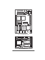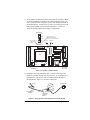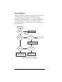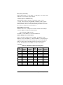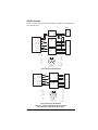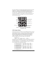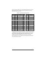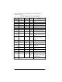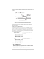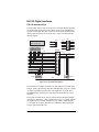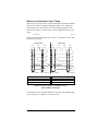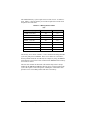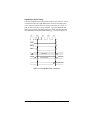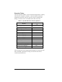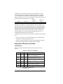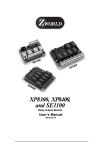
1
BL1300 C-Programmable Controller Users Manual Revision 3 Z-World BL1300 Users Manual Part Number 019-0006-03 Revision 3 021-0021-03 Printed in U.S.A. Last Revised by TI August 25, 1998 Copyright © 1998 Z-World, Inc. All rights reserved. Z-World reserves the right to make changes and improvements to its products without providing notice. Trademarks Dynamic C® is a registered trademark of Z-World. PLCBus is a trademark of Z-World. SmartBlock is a trademark of Z-World. Windows® is a registered trademark of Microsoft Corporation. Notice to Users When a system failure may cause serious consequences, protecting life and property against such consequences with a backup system or safety device is essential. The buyer agrees that protection against consequences resulting from system failure is the buyers responsibility. This device is not approved for life-support or medical systems. Company Address Z-World 2900 Spafford Street Davis, California 95616-6800 USA Telephone: Facsimile: 24-Hour FaxBack: Web Site: E-Mail: (530) 757-3737 (530) 753-5141 (530) 753-0618 http://www.z w orld.com [email protected] TABLE OF CONTENTS About This Manual vii Overview 1-1 Getting Started 2-1 BL1300 Operation 3-1 System Development 4-1 BL1300 Overview .............................................................................. 1-2 SmartBlock Features .......................................................................... 1-4 Options and Upgrades ........................................................................ 1-5 Software Development and Evaluation Tools .................................... 1-5 Initial BL1300 Setup .......................................................................... 2-2 Parts Required ............................................................................... 2-2 Connecting the BL1300 to a Host PC ................................................ 2-2 Running Dynamic C ........................................................................... 2-5 Test the Communication Line ....................................................... 2-5 Selecting Communications Rate, Port, and Protocol .................... 2-5 Running a Sample Program ............................................................... 2-5 Operating Modes ............................................................................... Run Mode ...................................................................................... Changing Baud Rate on the BL1300 ............................................ EPROM .............................................................................................. Programming EPROMs ................................................................ Choosing EPROMs ....................................................................... Copyrights ..................................................................................... 3-2 3-3 3-3 3-3 3-3 3-4 3-5 Dynamic C Libraries .......................................................................... 4-2 Data Communication ......................................................................... 4-3 Parallel Communication ................................................................ 4-3 Serial Communication ................................................................... 4-3 Z180 Serial Ports ............................................................................... 4-7 ASCI Status Registers ................................................................... 4-9 ASCI Control Register A .......................................................... 4-10 ASCI Control Register B .......................................................... 4-12 Software Drivers for Z180 Serial Ports ....................................... 4-14 BL1300 Table of Contents s iii Serial Communication Controller Ports ........................................... 4-16 RS-485 Network ......................................................................... 4-17 SCC Baud Rate Generation ......................................................... 4-19 SCC Software Drivers ................................................................. 4-21 Parallel Communication ................................................................... 4-24 Parallel Connections ................................................................... 4-24 Using Protocol Switch PIOs ....................................................... 4-27 Use BL1300 to Drive a Printer ................................................. 4-27 BL1300 Printer Emulation ........................................................ 4-28 BL1300 Digital Interfaces ............................................................... 4-29 PIO LSI Interface Chip ............................................................... 4-29 Using PIO Ports ........................................................................ 4-31 References 5-1 Appendix A: Troubleshooting A-1 Appendix B: Specifications B-1 Out of the Box .................................................................................... A-2 Dynamic C Will Not Start .................................................................. A-2 Dynamic C Loses Serial Link ............................................................ A-3 BL1300 Resets Repeatedly ................................................................ A-3 Interrupts Off for Long Periods ......................................................... A-3 Input/Output Problems ....................................................................... A-3 Power-Supply Problems ..................................................................... A-3 Common Programming Errors ........................................................... A-4 Hardware Dimensions ........................................................................ B-2 Jumper and Header Specifications ..................................................... B-4 Appendix C: Memory, I/O Map, and Interrupt Vectors C-1 BL1300 Memory ............................................................................... C-2 Physical Memory .......................................................................... C-2 Memory and Input/Output Cycle Timing ...................................... C-3 Input/Output Cycle Timing ......................................................... C-5 Execution Timing .......................................................................... C-6 Memory Map ..................................................................................... C-7 Input/Output Select Map ............................................................... C-7 Z180 Internal Input/Output Registers Addresses 00-3F ................ C-8 KIO Registers 0040-004F on Dynamic Interface Board (8-bit decode) ........................................................................... C-10 BL1300 Registers 0080-00D0 (8-bit decode) ............................ C-11 Epson 72421 Timer Registers 4000-400F .................................. C-12 Other Addresses .......................................................................... C-12 iv s Table of Contents BL1300 Interrupt Vectors .............................................................................. C-13 Nonmaskable Interrupts .............................................................. C-14 Power Failure Interrupts ........................................................... C-14 Jump Vectors ............................................................................... C-15 Interrupt Priorities ....................................................................... C-16 Initialized RAM Locations .............................................................. C-16 Appendix D: SmartBlock Subsystems D-1 Appendix E: PLCBus E-1 Appendix F: Simulated PLCBus Connection F-1 Appendix G: Power Management G-1 Appendix H: Hardware Configuration H-1 EEPROM Parameters ........................................................................D-2 Library Routines ................................................................................D-3 Time/Date Clock ................................................................................D-3 Time/Date Functions .....................................................................D-4 Watchdog Timer .................................................................................D-5 Use of Watchdog Timer ................................................................D-5 PLCBus Overview ............................................................................. E-2 Allocation of Devices on the Bus ...................................................... E-6 4-Bit Devices ................................................................................ E-6 8-Bit Devices ................................................................................ E-7 Expansion Bus Software .................................................................... E-7 BL1300 .............................................................................................. F-2 Power Consumption ...........................................................................G-2 Intermittent Operation ........................................................................G-2 Appendix I: Battery I-1 Battery Life and Storage Conditions ................................................... I-2 Replacing Soldered Lithium Battery ................................................... I-2 Battery Cautions ................................................................................. I-3 Index Schematics BL1300 Table of Contents s v vi s Table of Contents BL1300 ABOUT THIS MANUAL This manual provides instructions for installing, testing, configuring, and interconnecting the Z-World BL1300 controller. Instructions to get started using Dynamic C programming functions are included. Complete C and Dynamic C references and programming resources are referenced when necessary. Assumptions Assumptions are made regarding the user's knowledge and experience in the following areas: Ability to design and engineer the target system that a BL1300 will control. Understanding of the basics of operating a software program and editing files under Windows on a PC. Knowledge of the basics of C programming. $ For a full treatment of C, refer to the following texts. The C Programming Language by Kernighan and Ritchie (published by Prentice-Hall). and/or C: A Reference Manual by Harbison and Steel (published by Prentice-Hall). Knowledge of basic Z80 assembly language and architecture. $ For documentation from Zilog, refer to any of the following texts. Z180 MPU User's Manual Z180 Serial Communication Controllers Z80 Microprocessor Family User's Manual BL1300 About This Manual s v Acronyms Table 1 lists acronyms that may be used in this manual. Table 1. Acronyms Acronym Meaning EPROM Erasable Programmable Read Only Memory EEPROM Electronically Erasable Programmable Read Only Memory NMI Nonmaskable Interrupt PIO Parallel Input/Output Circuit (Individually Programmable Input/Output) PRT Programmable Reload Timer RAM Random Access Memory RTC Real Time Clock SIB Serial Interface Board SRAM Static Random Access Memory UART Universal Asynchronous Receiver Transmitter Conventions Table 2 lists and defines the typographic conventions that may be used in this manual. Table 2. Typographic Conventions Example Description While Courier font (bold) indicates a program, a fragment of a program, or a Dynamic C keyword or phrase. // IN-01… Program comments are written in Courier font, plain face. Italics Indicates that something should be typed instead of the italicized words (e.g., in place of filename, type a file’s name). Edit Sans serif font (bold) signifies a menu or menu selection. ... An ellipsis indicates that (1) irrelevant program text is omitted for brevity or that (2) preceding program text may be repeated indefinitely. [ ] Brackets in a C function’s definition or program segment indicate that the enclosed directive is optional. < > Angle brackets occasionally enclose classes of terms. a|b|c A vertical bar indicates that a choice should be made from among the items listed. vi s About This Manual BL1300 Programming Pseudo Types For convenience, this manual uses the following pseudo types: uint means unsigned integer ulong means unsigned long These pseudo types are not standard C keywords; therefore, they will not function in an application unless first declared with typedef or #define. A black square indicates pin 1 of all headers. Pin 1 J1 Pin Number 1 Measurements All diagram and graphic measurements are in inches followed by millimeters enclosed in parenthesis. Icons Table 3 displays and defines icons that may be used in this manual. Table 3. Icons Icon $ ( Meaning Refer to or see Please contact Caution ! Note High Voltage 7,3 FD BL1300 Tip Factory Default About This Manual s vii viii s About This Manual BL1300 OVERVIEW Chapter 1 provides an overview and a brief description of the BL1300 features. BL1300 Overview s 1-1 BL1300 Overview The BL1300 is a general-purpose communications hub that transfers and controls data across any of its six communication ports, with an emphasis on supporting IBM PC or compatible computers. The BL1300 consists of a main board with a Z-World SmartBlockTM that provides the processing power, as shown in Figure 1-1. DB25 Connector 26-pin square connectors parallel ports SmartBlock Microprocessor Module Reset Pushbutton RS-232 Drivers RS-485 Drivers DIN Connectors Figure 1-1. BL1300 Features Figure 1-2 shows the layout of the main board and Figure 1-3 shows the layout for the SmartBlock. Two ASCI serial ports (1 and 2) are implemented using the serial ports of the Z180 microprocessor chip. These RS-232 ports are asynchronous. Both Zilog Serial Communication Controller (SCC) serial ports (3 and 4) can be configured as either RS-485/RS-422 or RS-232 interfaces, and are implemented using the SCC. The SCC supports both asynchronous and synchronous communications with various protocols, such as SDLC, HDLC and Bisync. The clock can be transmitted on a separate signal line or embedded in the data signal using any of several standard techniques. Either full-duplex or half-duplex can be implemented in RS-485 multidrop systems. 1-2 s Overview BL1300 U12 J4 P05 J16 J2 J6 P6 J5 P5 Jack PIO U7 U9 U10 J3 PIO J9 J8 RP4 J11 LEDs P3 P4 J1 P2 P1 J10 J7 U5 U4 U3 U1 J12 J14 RP1 RP2 RP3 SCC U2 J15 J13 U6 U8 PAL Reset Pushbutton Figure 1-2. BL1300 Main Board Layout J7 J8 J3 J2 J1 U4 U2 U3 CLOCK U1 PAL EEPROM U5 Z180 J4 SRAM U6 U7 Supervisor J5 EPROM CRYSTAL J6 R5 J10 Figure 1-3. SmartBlock Layout BL1300 Overview s 1-3 The BL1300 has two 16-bit parallel ports with 16 lines that can be configured as a Centronics style interface. Each line can be configured as a TTL-level input or output. The lines can be programmed to interrupt the microprocessor in response to various external signals. The ports are implemented with the Zilog PIO. Cabling and software make it easy to use these ports for bidirectional communications with a PC bidirectional printer port. The maximum data rate is approximately 60,000 bytes per second from the computer to the BL1300, or 30,000 bytes per second to the PC. The parallel ports are general and can be used for other purposes, such as driving industrial I/O Opto 22 racks. The BL1300 can be mounted in the standard enclosure shown in Figure 1-4. The four mounting holes in the board can be used to mount the board in another enclosure. Screw holes are also provided to fasten the SmartBlock to the main board for high-vibration environments. Figure 1-4. Optional BL1300 Enclosure SmartBlock Features Z180 microprocessor running at 9.216 MHz Memory management unit (MMU) to address 1M Two programmable reload timers Two DMA channels. Two asynchronous serial ports One clocked serial port Dynamic Random Access Memory (DRAM) refresh unit Wait state generator Interface device for Motorola-type peripherals 32K SRAM with provision for battery backup, also accepts 128K, 256K, or 512K memory chips with 28 or 32 pins 32K EPROM, also accepts up to 256K chips with 28 or 32 pins 1-4 s Overview BL1300 Epson 72421 battery backed time of day clock. 512 byte EEPROM, the upper 256 bytes can be write-protected Microprocessor supervisor provides power fail detect, power on reset, battery backup and watchdog timer. 18.432 MHz system crystal providing a 9.216 MHz microprocessor clock Lithium backup battery $ Appendix B provides detailed specifications for the BL1300. Options and Upgrades The following accessories are available for the BL1300. Protective enclosure Developers kit with RS-485/RS-422 driver chips and resistor packs for RS-485 multidrop networks Switching power regulator Mini DIN-8 to DB25M cable Mini DIN-8 to DB9F null modem cable Mini DIN-8 to bare leads cable ( For ordering information, or for more details about the various options and prices, call your Z-World Sales Representative at (530) 757-3737. Software Development and Evaluation Tools Dynamic C, Z-Worlds Windows-based real-time C language development system, is used to develop software for the BL1300. The host PC downloads the executable code through the Dynamic C Interface Board to one of the following places: battery-backed RAM, or ROM written on a separate ROM programmer and then substituted for the standard Z-World ROM. This allows fast in-target development and debugging. $ BL1300 Z-Worlds Dynamic C reference manuals provide complete software descriptions and programming instructions. Overview s 1-5 1-6 s Overview BL1300 GETTING STARTED Chapter 2 provides instructions for connecting the BL1300 to a host PC and running a sample program. BL1300 Getting Started s 2-1 Initial BL1300 Setup Parts Required 24 V unregulated DC power supply Programming cable Dynamic C Interface Board Connecting the BL1300 to a Host PC 1. Connect the power supply to the BL1300 power supply jack J4. Do not plug the transformer into the wall until all the connections and jumpers have been set. 2. Check the drivers in positions U1, U2, U3, and U4. The factoryinstalled LT1180 chips at U1 and U2 support RS-232 communication at P3 and P4. To enable the RS-485/RS-422 ports at P3 and P4, remove the LT1180 drivers from U1 and U2, and install a 75175 in U3 and a 75174 in U4. Figure 2-1 illustrates the locations. Only one set of drivers may be installed in U1/U2 or U3/U4 at one time. The ports will not work if both sets of drivers are installed at the same time, and the components may be damaged. RP4 P4 P3 P2 P1 J10 J1 J11 J7 U5 U3 U4 SCC U2 U1 RP1 RP2 RP3 ( For information about the BL1300 accessory kit containing the RS-485 drivers, call your Z-World Sales Representative at (530) 757-3737. Reset Pushbutton Figure 2-1. Location of Driver Chips and Serial Ports 2-2 s Getting Started BL1300 3. Set the jumpers on jumper block J04 of the Dynamic C Interface Board for RS-232 or RS-485 according to the communication protocol to be used. Set the baud rate using pins 3-4 and 5-6 on jumper block J07 on the Interface Board. Connect pins 1-2 on J07 to run the program in the battery-backed RAM on reset, instead of Dynamic C. Figure 2-2 shows the Interface Board and its jumper configurations. Baud Rate 57,500 28,800 Connect pins 7-8 to disable Interface Board (behave as if not connected) 19,200 9600 Connect pins 1-2 to run program in RAM RS-485 RS-232 2 4 6 8 1012 14 16 J01 15 1 J06 J04 RS-485 RS-232 J07 U03 U01 KIO U04 U02 J02 U05 Reset Button U06 R1 J05 Jack J03 J08 40-pin connection to BL1300 SmartBlock Leave disconnected DC Power Connector Figure 2-2. Dynamic C Interface Board 4. Establish a serial communications link. Connect header J06 on the Dynamic C Interface Board to the 40-pin header, J1, on the BL1300s SmartBlock. The 40-wire cable is included with the Dynamic C Interface Board. Figure 2-3 shows the connections. To PC 300 BL1 Transformer J1 J06 Programming Cable J01/J02 Dynamic C Interface Board Figure 2-3. Using Dynamic C Interface Board to Program BL1300 BL1300 Getting Started s 2-3 A PC communicates with the BL1300 via the Dynamic C Interface Board using an RS-232 or an RS-485 serial link. There are two 10-pin serial headers on the Dynamic C Interface Board, one for RS-232 communication (J01) and one for RS-485 communication (J02). Connect the programming cable to the appropriate header. Figure 2-4 shows the programming cable included in the developers kit. To PC 6 9 1 To PC 5 3M 3631 3M 3473 9 9-pin to 25-pin adapter (optional) 2 3 1 To Dynamic C Interface Board Figure 2-4. BL1300 Developers Kit Programming Cable Although the Interface Board has its own power supply connections at J03, as shown in Figure 2-2, do not connect the transformer to the Interface Board. The Interface Board will receive its power through the 40-wire cable connecting it to the BL1300 SmartBlock. The reset button on the Interface Board is connected in parallel with the reset button on the BL1300. 5. Connect pins 2-3 on SmartBlock jumper block J2 to write-enable the EEPROM. Connect the pins on SmartBlock jumper block J3 to enable the watchdog timer. $ See Appendix D, SmartBlock Subsystems, for more information about the EEPROM. 6. The BL1300 is now ready for programming. The power supply transformer may be plugged in and turned on. 2-4 s Getting Started BL1300 Running Dynamic C Test the Communication Line Double-click the Dynamic C icon to start the software. Note that the PC attempts to communicate with the BL1300 each time Dynamic C is started. No error messages are displayed once communication is established. $ ! See Appendix A, Troubleshooting, if an error message such as Target Not Responding or Communication Error appears. Once the necessary changes have been made to establish communication between the host PC and the BL1300, use the Dynamic C shortcut Ctrl Y to reset the controller and initiate communication. Selecting Communications Rate, Port, and Protocol The communication rate, port, and protocol are all selected by choosing Serial Options from Dynamic Cs OPTIONS menu. The BL1300s default communication rate is 19,200 bps. However, the Dynamic C software shipped by Z-World may be initialized for a different rate. To begin, adjust the communications rate to 19,200 bps. Make sure that the PC serial port used to connect the serial cable (COM1 or COM2) is the one selected in the Dynamic C OPTIONS menu. Select the 1-stop-bit protocol. Running a Sample Program A sample program, PSFLASH.C, is supplied in the Dynamic C SAMPLES subdirectory. This program flashes the LEDs on the board. Prior to running this test, be sure to set the communications parameters in Dynamic C so that the PC and the BL1300 are handshaking properly. 1. Compile the program by pressing F3 or by choosing Compile from the COMPILE menu. Dynamic C compiles and downloads the program. 2. Run the program by pressing F9 or by choosing Run from the RUN menu. The LEDs on the BL1300 will begin flashing continuously. 4. Press Ctrl Z to stop execution of the program. 5. If needed, press F9 to restart execution of the program. The Dynamic C SAMPLES subdirectory contains other sample programs that illustrate the features of the BL1300. These programs may be used as a basis for new applications. BL1300 Getting Started s 2-5 2-6 s Getting Started BL1300 BL1300 OPERATION Chapter 3 describes how to use the BL1300, with a focus on how to set the run and programming modes, and how to burn a custom program on EPROM. BL1300 Operation s 3-1 Operating Modes A hardware reset takes place when the BL1300 is powered up, when the reset button is pressed, or when the watchdog timer times out. If a valid program (created with Dynamic C) has been installed in EPROM, the program starts running. A valid program is recognized by a code that Dynamic C places in the file used to burn the EPROM. The flowchart in Figure 3-1 shows the startup sequence of the BL1300 after a hardware reset. Begin from hardware reset Valid program in YES EPROM? Run program. Dynamic C Interface board connected? Dynamic C Interface Board connected? Valid program in RAM? NO Error halt YES YES Run application in RAM. YES Interface Board J07:1-2 connected? YES Valid program in RAM? NO Run Dynamic C at baud rate specified by Interface Board J07:3-4 & J07:5-6 Flash Error Signal LED 4 Figure 3-1. BL1300 Activity at Startup 3-2 s Operation BL1300 Run Mode Before running a program from battery-backed RAM, be sure pins 1 and 2 on jumper block J07 of the Dynamic C Interface Board are connected. If a valid user program is already in EPROM, that program will run when the reset button is pushed. ! If the Dynamic C EPROM is present on the board, the BL1300 executes the program stored in battery-backed RAMthat is, the program last run under Dynamic C. If the Dynamic C EPROM has been replaced with a custom EPROM, then the BL1300 executes that program. Changing Baud Rate on the BL1300 The baud rate may be changed by connecting the appropriate pins on jumper block J07 of the Dynamic C Interface Board, as shown in Figure 2-2, then pushing the reset button. Be sure the power to the BL1300 is disconnected before changing any jumper connections. EPROM Programming EPROMs Dynamic C can be used to create a file for programming an EPROM by selecting the Compile to File option in the COMPILE menu. The BL1300 must be connected to the PC running Dynamic C during this step because essential library routines must be uploaded from the Dynamic C EPROM and linked to the resulting file. The output is a binary file (optionally an Intel hex format file) that can be used to build an application EPROM. The application EPROM is then programmed with an EPROM programmer that reads either a binary image or the Intel hex format file. The resulting application EPROM can then replace the EPROM that came with the BL1300. Whenever the Dynamic C EPROM is replaced by a custom EPROM, the BL1300 ignores the program in battery-backed RAM in favor of the program stored in EPROM. When doing program development with Dynamic C, it is best to use a 128K SRAM or larger. Dynamic C will work with a 32K SRAM, but the total program space will be limited to 16K of root and 16K of extended memory. This is enough for many programs, but it is inconvenient to run BL1300 Operation s 3-3 out of memory during development. Once a program is burned into EPROM, there is no reason to use SRAM larger than 32K unless the data space is larger than 32K. Choosing EPROMs Socket U6 can accommodate several different types of EPROMs, including the following. 27C256 27C512 27C010 27C020 32K 64K 128K 256K 28 pins 28 pins 32 pins 32 pins When using a 28-pin EPROM, four pin positions at one end of the socket are left empty, as shown In Figure 3-2. U5 J4 U1 U5 28-pin SRAM U6 U6 EPROM J5 32-pin SRAM J4 EPROM J5 J6 J6 Figure 3-2. Placement of 28-pin and 32-pin EPROMs on BL1300 The corresponding jumper settings for jumper blocks J4, J5, and J6 are shown in Figure 3-3. J4 J5 J6 64K or larger EPROM 32K128K SRAM 256K512K SRAM FD 32K EPROM 32-pin EPROM FD 28-pin EPROM FD Figure 3-3. BL1300 Jumper Settings for Different-Sized SRAM and EPROM Either 28-pin or 32-pin SRAM chips may be used. 3-4 s Operation BL1300 Copyrights The Dynamic C library is copyrighted. Place a label containing the following copyright notice on the EPROM whenever an EPROM that contains portions of the Dynamic C library is created. ©19911995 Z-World, Inc. Your own copyright notice may also be included on the label to protect your portion of the code. Z-World grants purchasers of the Dynamic C software and the copyrighted SmartBlock EPROM permission to copy portions of the EPROM library as described above, provided that: 1. The resulting EPROMs are used only with the BL1300 controllers manufactured by Z-World, Inc., and 2. Z-Worlds copyright notice is placed on all copies of the EPROM. BL1300 Operation s 3-5 3-6 s Operation BL1300 SYSTEM DEVELOPMENT Chapter 4 provides the following information to develop the BL1300 for specific uses. Dynamic C libraries Data communication Serial ports Serial Communication Controller ports Parallel communication Digital interfaces BL1300 System Development s 4-1 Dynamic C Libraries Functions specific to the BL1300 can be found in the software libraries supplied with Dynamic C. These libraries are maintained in source code so they can be easily modified or augmented by the user. The BL1300 functions are in the BL13XX.LIB, DRIVERS.LIB, PRPORT.LIB, and SERIAL.LIB libraries. Whenever unresolved calls to functions remain after an application is compiled, Dynamic C scans all the source libraries for functions with that name. When found, the functions are extracted from the library and are compiled with the application. The libraries are scanned until no more unresolved names are found, so library functions can call other library functions and their order of appearance in the library is not important. Dynamic C also accesses a library in the EPROM on the BL1300 board. This library is in machine language and the library functions can be called directly from a program. This library has the advantage that the code does not need to be downloaded, reducing the compile time, particularly for the standard version of Dynamic C with its slower communication rate. The EPROM library version is used if the same function appears in both the EPROM library and the source library. Use the following preprocessor command to replace a function in the EPROM library. #KILL func1, func2, func3 . . . This causes the specified functions in the EPROM library to be ignored. Replaceable functions in the EPROM library have a period (.) in their name. The KILL directive will change the period to an underscore (_), causing a search for a legal C name to occur. Your own version of the function can then be added to the program or taken from one of the libraries. 4-2 s System Development BL1300 Data Communication The BL1300 is capable of both parallel and serial communication. These options are described briefly in the following sections. Parallel Communication Parallel communication uses four or eight data paths to transfer data. In serial communication, a single bit at a time is transferred, and only one data path in the direction of transmission is required (two data paths are required if an external data clock is used). Parallel communication can be much faster, but is more expensive because of the need for multiple communication lines. Personal computers are usually equipped with a parallel communication port to drive a printer. It is possible to communicate between the PC and the BL1300 using such a parallel port at a much higher data rate than can be obtained with a serial port, that is, about 40,000 bytes per second out of the PC and 10,000 bytes per second to the PC. The maximum rate possible on a serial port is 115,200 bits per second. The parallel interface capability of the BL1300 makes it suited for many jobs that could otherwise only be accomplished by using special interface cards plugged into the PC. Parallel communication uses an interlocked handshake so that data are not lost if the PC or BL1300 get distracted by higher priority tasks. This high-speed protocol is discussed in more detail later in this chapter. Serial Communication The serial data communication modes available on the BL1300 are variations of asynchronous and synchronous protocols, as shown in Figure 4-1. Asynchronous serial communication is characterized by individual data characters prefixed by a start bit and terminated by at least one stop bit, with optional parity bits. Asynchronous data can be sent slowly, with arbitrary gaps between characters. At least 10 bits must be sent to transmit eight data bits. Data are sent with the least significant bit first. Figure 4-2 shows the format of a single character. Besides the overhead of the start and stop bits, another disadvantage to asynchronous communication is the chance that the communications will get out of sync with the data stream. This can occur if the data are sent continuously, with the next start bit immediately following the last stop bit. Although asynchronous communications can run at high speeds, particularly if a separate clock line is used, it is more commonly used at lower speeds of 115,200 bps or less. BL1300 System Development s 4-3 Serial Synchronous Clock External Clock Clock Recovered from Data Mode Monosync Bisync SDLC Encoding NRZ, NRZI, FM0, FM1 Signal Level Unbalanced (RS-232) Balanced (RS-485) Asynchronous Clock Internal, external Modes Parity, stop bits, data bits Signal Level Unbalanced (RS-232) Balanced (RS-485) Figure 4-1. Serial Communication Protocols T=1/baud_rate S D D D D D D D Data Bits 7 or 8 Start Bit D P Parity Bit ST ST Stop Bits 1, 1.5 or 2 RS-232 voltage levels are shown Figure 4-2. Format of Single Character in Asynchronous Serial Communication 4-4 s System Development BL1300 Synchronous communication does not use start and stop bits. It requires a separate clock and a regular procedure for detecting the start of a message and identifying the first bit. The clock can either be transmitted on a completely separate line or embedded in the signal and then extracted by a phase-locked loop. SDLC is the most popular synchronous transmission method. SDLC is a bit stream made up of a multiple of 8-bit bytes. It follows the rule that no more than five 1s can appear consecutively in the data stream, and enforces this rule by inserting a 0 following any group of five 1s. The receiver deletes any zeros following five 1s, thus reversing the insertion of the spurious zeros. A special flag character, 01111110, with six 1s is used to mark the start and end of a frame of data. A few other special characters with more than five 1s are used for control. This bit stuffing algorithm guarantees that there will be transitions in the data stream when using NRZI encoding of the data. This makes it possible to recover the clock from the data stream using a phase-locked loop. A phase-locked loop observes transitions in the data stream and keeps internal clock transitions lined up with the transitions in the data by speeding up or slowing down the internal clock by a small amount. An SDLC data frame is followed by a special 2 byte cyclic redundancy check word having a high probability of detecting errors in the data stream. All bit stuffing and check sums are handled by hardware, allowing very high data rates of millions of bits per second. Direct Memory Access (DMA) transfers are necessary at baud rates above 400,000 bits per second since data cannot be handled by programmed inputs/outputs at such speeds. DMA transfers use special hardware to move data directly between the microprocessor memory and the serial port. Various errors can occur in serial communication. When a low is detected where a stop bit should be, this is called a framing error. An overrun error occurs if data come in faster than the microprocessor removes it, to the point where the input queue overflows. A parity error occurs if parity is enabled and the parity bit is not correct (it can be even or odd parity). Serial data are often transmitted over wires using unbalanced (RS-232) or balanced (RS-485/RS-422) voltage-level signaling. RS-232 signaling is used by the standard IBM PCs COM port. The voltage levels range from 6 V for a 1 to +6 V for a 0. RS-232 is suitable only for low to moderate speeds over short distances, such as 15 m (50 ft). RS-485 signaling is over a twisted-pair transmission line using balanced signalinga 1 indicates that the + signal is higher than the signal, while a 0 indicates the opposite. This type of signaling is suitable for longer distances and data rates, such as 100,000 bits per second at 1000 m. Slower speeds and thicker wire allow even greater distances. Usually the voltage swing on BL1300 System Development s 4-5 each side of a balanced pair is 0 V to 2 V, although the standard allows a much greater range and a considerable difference in ground potential between the two sides of the link. RS-485 communication can be full-duplex or half-duplex. In half-duplex, the transmitter sends a message, then stops driving the transmission line. The receiver can then begin to drive the line and send a reply. Data are sent in one direction at a time and only a single twisted pair plus ground is necessary. In full-duplex, a twisted pair in each direction is needed. The communication is multidrop if a number of stations listen to the messages at one time and have the option of replying. The twisted-pair communication lines must be terminated by their characteristic impedance and biased if there are times when no transmitter is driving the line. Modems are used to transmit data over the universal telephone system or over lines too long for RS-485. Modems are also used for broadband systems where many data signals are multiplexed at radio frequencies over coaxial cable, radio, or microwave. Modems convert the high and low voltage levels to shifts in frequency or phase of the signal in such a way that the signal is not degraded by the transmission. 4-6 s System Development BL1300 Z180 Serial Ports Two of the BL1300s serial ports use the asynchronous serial controller interface (ASCI) built into the Z180 microprocessor. These ports are available through P1 (Channel 0) and P2 (Channel 1) of the ASCI. These ports can deliver a maximum baud rate of 57,600 bps with the standard 9.216 MHz system clock. There is a separate baud-rate generator for each channel. The baud rate can be divided down from the microprocessor clock for either channel. One of the internal DMA controllers can be used with the internal serial ports. Figure 4-3 shows the signals available on jacks P1 and P2. MINI8 TXA0 /TXA0 RXA0 /RXA0 RS-232 TXA1 U6 /TXA1 RXA1 /RXA1 Z180_TXA0 Z180_RXA0 Z180_TXA1 Z180_RXA1 Z180 SCC_/DTRA SCC_/DCDA P1 (z0) 1 RTS0 2 CTS0 6 TX 8 RX Shield GND 6 4 2 P6 P8 P2 P1 P2 P2 (z1) 7 8 5 P1 P1 P2 /RTS0 RTS0 /CTS0 CTS0 RS-232 U7 /DTRA DTRA /DCDA DCDA Z180_/RTS0 Z180_/CTS0 SCC P6 P8 1 3 1 DTRA (SCC) 2 DCDA (SCC) 6 TX 8 RX Shield GND 2 4 J1 1 P4 P4 P7 3 Back Side of DIN Connector Figure 4-3. Signals on BL1300 on P1 and P2 Jacks, ASCI Channels 0 and 1, RS-232 Driver Chips The serial ports have an optional multiprocessor communication feature. When enabled, an extra bit is included in the transmitted character where the parity bit would normally go. Receiving Z180s can be programmed to ignore all received characters except those with the extra multiprocessing bit set. This provides a 1 byte attention message that can wake up a processor without the processor having to intelligently monitor all traffic on a shared communications link. The block diagram in Figure 4-4 shows Serial Channel 0. Serial Channel 1 is similar, but modem control lines RTS1 and CTS1 are not available directly. DTR and DCD from the serial communication controller can be used if handshaking lines are required for Channel 1. Five of the seven registers are directly accessible as internal I/O registers. BL1300 System Development s 4-7 microprocessor internal bus RXA0 RDR0 TDR0 RSR0 TSR0 Shift Register In RTS0 CTS0 DCD0 CNTLA0 Baud Rate Generator CNTLB0 TXA0 Shift Register Out CLKA0 STAT0 Figure 4-4. Z180 Serial Channel 0 A separate interrupt vector is used by each of the two channels. The interrupt vectors are SER0_VEC and SER1_VEC. The Channel 0 interrupt has the higher priority. The serial ports can be polled or interrupt-driven. A polling driver tests the ready flags (TDRE and RDRF) until a ready condition appears (transmitter data register empty or receiver data register full). If an error condition occurs on receive, the routine must clear the error flags and take appropriate action, if any. If the CTS line is used for flow control, transmission of data is automatically stopped when CTS goes high because the TDRE flag is disabled. This prevents the driver from transmitting more characters because the driver thinks the transmitter is not ready. The transmitter will still function with CTS high, but care should be exercised since TDRE is not available to properly synchronize loading of the data register (TDR). An interrupt-driven port works when the receiver interrupt is enabled as long as the program wants to receive characters. The transmitter interrupt is enabled only while characters are waiting in the output buffer. When an interrupt occurs, the interrupt routine must determine the cause: receiver data register full, transmitter data register empty, or receiver error. All of these interrupts are level-triggered, and another interrupt will occur immediately if the interrupts are re-enabled without disabling the condition causing the interrupt. 4-8 s System Development BL1300 ASCI Status Registers The Z180 incorporates an asynchronous serial communication interface (ASCI) that supports two independent full-duplex channels. Appendix C summarizes the addresses of these registers. A status register for each channel provides information about the state of each channel and allows interrupts to be enabled and disabled. STAT0 (04H) 7 6 5 4 3 2 1 0 RDRF OVRN PE FE RIE /DCD0 TDRE TIE R R R R R/W R R R/W STAT1 (05H) 7 6 5 4 3 2 1 0 RDRF OVRN PE FE RIE CTS1E TDRE TIE R R R R R/W R/W R R/W /DCD0 (Data Carrier Detect) This bit echoes the state of the /DCD0 input pin for Serial Channel 0. However, when the input to the pin switches from high to low, the data bit switches low only after STAT0 has been read. The receiver is held reset as long as the input pin is held high. This function is not generally useful because an interrupt is requested as long as /DCD0 is a 1. This forces the programmer to disable the receiver interrupts to avoid endless interrupts. A better design would cause an interrupt only when the state of the pin changes. This pin is tied to ground. TIE (Transmitter Interrupt Enable) This bit masks the transmitter interrupt. If set to 1, an interrupt is requested whenever TDRE is 1. The interrupt is not edge triggered. This bit must be set to 0 when there is a need to stop sending. Otherwise, interrupts will be requested continuously as soon as the transmitter data register is empty. TDRE (Transmitter Data Register Empty) A 1 means that the channel is ready to accept another character. A high level on the /CTS pin forces this bit to 0 even though the transmitter is ready. CTS1E (CTS Enable, Channel 1) The signals RXS and CTS1 are multiplexed on the same pin. A 1 stored in this bit selects the pin to serve the CTS1 function. A 0 selects the RXS function. (The pin RXS is the CSIO data receive pin.) The CTS line has no effect when RXS is selected. It is not advisable to use the CTS1 function on the BL1300 because the RXS line is needed to control several other devices on the board. BL1300 System Development s 4-9 RIE (Receiver Interrupt Enable) A 1 enables receiver interrupts and 0 disables them. A receiver interrupt is requested under any of the following conditions: /DCD0 (Channel 0 only), RDRF (receiver data register full), OVRN (overrun), PE (parity error), FE (framing error). The condition causing the interrupt must be removed before interrupts are re-enabled, or another interrupt will occur. Reading the receiver data register (RDR) clears the RDRF flag. The EFR bit in CNTLA is used to clear the other error flags. FE (Framing Error) A stop bit was missing, indicating scrambled data. This bit is cleared by the EFR bit in CNTLA. PE (Parity Error) Parity is tested only if MOD1 in CNTLA is set. This bit is cleared by the EFR bit in CNTLA. OVRN (Overrun Error) Overrun occurs when bytes arrive faster than they can be read from the receiver data register. The receiver shift register (RSR) and receiver data register (RDR) are both full. RDRF (Receiver Data Register Full) This bit is set when data are transferred from the receiver shift register to the receiver data register. It is always set when one of the error flags is set, in which case defective data are loaded to RDR. The bit is cleared when the receiver data register is read, when the /DCD0 input pin is high, and by RESET and IOSTOP. ASCI Control Register A Control Register A affects various aspects of the serial channel operation. CNTLA0 (00H) 7 6 5 4 3 2 1 0 MOD2 MOD1 MOD0 MPE RE TE /RTSO MPBR/ EFR R/W R/W R/W R/W R/W R/W R/W R/W 5 4 3 2 1 0 MOD2 MOD1 MOD0 R/W R/W R/W CNTLA1 (01H) 7 6 MPE RE TE R/W R/W R/W 4-10 s System Development MPBR/ CKA1D EFR R/W R/W BL1300 MOD0MOD2 (Data Format Mode Bits) MOD0 controls stop bits: 0 ⇒ 1 stop bit, 1 ⇒ 2 stop bits. If 2 stop bits are expected, then 2 stop bits must be supplied. MOD1 controls parity: 0 ⇒ parity disabled, 1 ⇒ parity enabled. (See PEO in ASCI Control Register B for even/odd parity control.) MOD2 controls data bits: 0 ⇒ 7 data bits, 1 ⇒ 8 data bits. MPBR/EFR (Multiprocessor Bit Receive/Error Flag Reset) Reads and writes on this bit are unrelated. Storing a byte when this bit is 0 clears all the error flags (OVRN, FE, PE). Reading this bit obtains the value of the MPB bit for the last read operation when multiprocessor mode is enabled. /RTS0 (Request to Send, Channel 0) Store a 1 in this bit to set the RTS0 line from the Z180 high. This line is further inverted by the output driver. This bit is essentially a 1-bit output port without other side effects. CKA1D (CKA1 Disable) This bit controls the function assigned to the multiplexed pin (CKA1/ TEND0): 1 ⇒ TEND0 (a DMA function) and 0 ⇒ CKA1 (external clock I/O for Channel 1 serial port). TE (Transmitter Enable) This bit controls the transmitter: 1 ⇒ transmitter enabled, 0 ⇒ transmitter disabled. When this bit is cleared, the processor aborts the operation in progress, but does not disturb TDR or TDRE. RE (Receiver Enable) This bit controls the receiver: 1 ⇒ enabled, 0 ⇒ disabled. When this bit is cleared, the processor aborts the operation in progress, but does not disturb RDR, RDRF, or the error flags. MPE (Multiprocessor Enable) This bit (1 ⇒ enabled, 0 ⇒ disabled) controls multiprocessor communication mode which uses an extra bit for selective communication when a number of processors share a common serial bus. This bit has effect only when MP in Control Register B is set to 1. When this bit is 1, only bytes with the MP bit on will be detected. Others are ignored. All bytes received are processed if this bit is 0. Ignored bytes do not affect the error flags or RDRF. BL1300 System Development s 4-11 ASCI Control Register B Control Register B for each channel configures the multiprocessor mode, parity, and baud rate selection. CNTLB0 (02H) and CNTLB1 (03H) 7 6 5 4 3 2 1 0 MPBT MP /CTS PS PEO DR SS2 SS1 SS0 R/W R/W R/W R/W R/W R/W R/W R/W SS (Source/Speed Select) Coupled with the prescaler (PS) and the divide ratio (DR) The SS bits select the source (internal or external clock) and the baud rate divider, as shown in Table 4-1. Table 4-1. Baud Rate Divide Ratios for Source/Speed Select Bits SS2 SS1 SS0 Divide Ratio 0 0 0 0 1 1 1 1 0 0 1 1 0 0 1 1 0 1 0 1 0 1 0 1 ÷1 ÷2 ÷4 ÷8 ÷ 16 ÷ 32 ÷ 64 external clock The prescaler (PS), the divide ratio (DR), and the SS bits form a baud-rate generator (see Figure 4-5). Processor Clock Prescaler (PS) ÷10 or ÷30 Divide Ratio (DR) Divider 1 2 ... 64 External Clock 16 or 64 Figure 4-5. Baud-Rate Generator DR (Divide Ratio) This bit controls one stage of frequency division in the baud-rate generator. If 1 then divide by 64. If 0 then divide by 16. This is the only control bit that affects the external clock frequency. 4-12 s System Development BL1300 PEO (Parity Even/Odd) This bit affects parity: 0 ⇒ even parity, 1 ⇒ odd parity. It is effective only if MOD1 is set in CNTLA (parity enabled). CTS/PS (Clear to Send/Prescaler) When read, this bit gives the state of external pin /CTS: 0 ⇒ low, 1 ⇒ high. When /CTS pin is high, RDRF is inhibited so that incoming receive characters are ignored. When written, this bit has an entirely different function. If a 0 is written, the baud rate prescaler is set to divide by 10. If a 1 is written, it is set to divide by 30. MP (Multiprocessor Mode) When this bit is set to 1, multiprocessor mode is enabled. The multiprocessor bit (MPB) is included in transmitted data. start bit, data bits, MPB, stop bits The MPB is 1 when MPBT is 1 and 0 when MPBT is 0. MPBT (Multiprocessor Bit Transmit) This bit controls the multiprocessor bit (MPB). The MPB is 1 when MPBT is 1 and 0 when MPBT is 0. When the MPB is 1, transmitted bytes will get the attention of other units listening only for bytes with MPB set. Table 4-2 relates ASCI Control Register B to the baud rate in bits per second. The baud rate at 18.432 MHz is, of course, twice that at 9.216 MHz. Table 4-2. Baud Rates for ASCI Control Register B Baud Rate at 9.216 MHz Baud Rate at 18.432 MHz (bps) (bps) 00 57,600 115,200 20 19,200 38,400 01 28,800 57,600 21 9600 19,200 02 or 08 14,400 28,800 22 or 28 4800 9600 03 or 09 7200 14,400 23 or 29 2400 4800 04 or 0A 3600 7200 24 or 2A 1200 2400 05 or 0B 1800 3600 25 or 2B 600 1200 06 or 0C 900 1800 26 or 2C 300 600 0D 450 900 2D 150 300 0E 225 450 2E 75 150 ASCI B Value BL1300 ASCI B Value Baud Rate at 9.216 MHz Baud Rate at 18.432 MHz (bps) (bps) System Development s 4-13 Software Drivers for Z180 Serial Ports A function to compute the control word for CNTLB0/CNTLB1 is built into the following function call. int z180baud( int clock, int baud ) This functions return the byte to be stored in CNTLB0/CNTLB1, considering only the bits needed to set the baud rate. Both the clock and baud rates are expressed in multiples of 1200. Thus a 9.216 MHz clock is expressed as 7680 and 19,200 bits per second is expressed by 16. The return value is 1 if the baud value cannot be derived from the given clock frequency. The function sysclock returns the system clock frequency in multiples of 1200 Hz. Each port is supported by four routines that control initialization, sending, receiving, and resetting. These routines are full-duplex, buffer-oriented, and interrupt-driven. These library functions can be used to send and receive messages on Serial Port 1. int int int int ser_init_z1( char mode, char baud ) ser_send_z1( char* buf, byte* count ) ser_rec_z1 ( char* buf, byte* count ) ser_kill_z1() The function ser_init_z1 initializes Serial Port 1 as specified. The mode parameter is a set of flags, as shown below. The baud parameter is expressed in multiples of 1200 bits per second. bit 0 0 1 1 stop bit 2 stop bits bit 1 0 1 no parity parity enabled bit 2 0 1 7-bit data 8-bit data bit 4 0 1 even parity odd parity For example, the statement below would initialize Port Z1 to communicate with 8 data bits, no parity, and 1 stop bit at 9600 baud. ser_init_z1(4,9600/1200); // Initialize ZIO port 1 After initialization, the functions ser_send_z1 and ser_rec_z1 are used to transfer data between the buffer and the serial port. The count parameter is decremented as characters are transferred. When count reaches zero, the transfer stops and the serial port is disabled. The calling program can monitor count to see the progress of the transfer. The ser_kill_z1 function immediately turns off both send and receive. 4-14 s System Development BL1300 ! Declare count to be a shared variable if the library functions are modified so that count is an int rather than a char. It is important to remember that the serial routines supplied with Dynamic C are interrupt-driven. This means that the transmission will continue in the background while the program is doing other things. Pointers are passing to a counter and a buffer. Both the counter and the buffer are changed by the interrupt routines. Always use static or global variables for the counter and buffer. A demonstration program, SER_DEMO.C, is available to demonstrate the use of the serial driver. ! The stack and the program will be corrupted if pointers to function variables stored on the stack are passed to the interrupt service routine and then that function is exited. ! Make count a shared variable if the library functions are modified so that count is larger than a byte. BL1300 System Development s 4-15 Serial Communication Controller Ports The serial communication controller (SCC) ports of the BL1300 can be configured to be either RS-232 or RS-485. They are factory-configured as RS-232 ports with RTS/CTS handshaking for both ports. SCC Channel A can also use the DCDA and DTRA signals when pins 13 and 24 on header J1 are connected. These signals are hardwired into jack P2, which is controlled by ZIO Channel 1, so care is needed when using both channels. Figure 4-6 shows the signals and jumper connections available to configure the SCC RS-232 ports. $ See Chapter 2, Getting Started, for details about enabling the RS-485 ports in jacks P3 and P4 by replacing the RS-232 driver chips with RS-485 driver chips. MINI8 P6 P8 RS-232 U7 SCC_/DTRA J14 SCC_/RTSA SCC_TXCA J15 SCC_/CTSA SCC P1 P2 /DTRA SCC_/DCDA DTRA DCDA /DCDA U2U4 SCC_RXCA SCC_TXDA 1 4 J1 3 P1 P4 P6 /TXDA P8 /RXDA RXDA P4 P7 P2 P42 U2 TXDA SCC_RXDA 2 P41 RS-232 U2U3 P2 J12 SCC_/RTSB SCC_TXCB J13 SCC_/CTSB U1U4 U1U3 SCC_RXCB SCC_TXDB SCC_RXDB P31 P1 P32 P2 /TXDA /RXDA P6 RS-232 U1 TXDA RXDA P3 P8 P4 (scc0) 1 P3 (scc1) 1 /CTSB RXCB 6 TX 8 RX Shield GND TXCA 6 2 TXCB or 7 8 or 2 /RTSA or /RTSB 5 4 2 or 3 1 Back Side of DIN Connector /CTSA RXCA 4 DTRA 7 DCDA 6 TX 8 RX Shield GND Figure 4-6. Signals on BL1300 on P3 and P4 Jacks, SCC Channels A and B, RS-232 Driver Chips 4-16 s System Development BL1300 RS-485 Network Figure 4-7 shows the signal flow and jumpers available for configuring the SCC RS-485 ports. MINI8 P6 P8 RS-232 U7 /DTRA /DCDA 2 SCC_/DTRA 1 SCC_/DCDA 4 J1 3 RS-485 J14 SCC_/RTSA SCC P2 P1 P2 DTRA DCDA U4 U2U4 SCC_TXCA TXDA SCC_TXDA P1 P4 P1 P4 P6 P3 P6 P3 P2 P7 P2 P7 P8 P5 P8 P5 J15 SCC_/CTSA U2U3 SCC_RXCA RS-485 SCC_RXDA U3 RXDA 4 P4 (scc0) 1 /RTS- TXC+ 7 8 TXC/CTS+ 6 4 5 or RXC+ 3 /RTS+ or or 2 P4 RX- 6 TX+ 7 3 2 5 /CTSor 1 RXC- TX- 8 Back Side of DIN Connector RX+ Shield GND (a) SCC Channel A, RS-485 Driver RS-485 J12 SCC_/RTSB SCC U4 U1U4 SCC_TXCB SCC_TXDB TXDB U1U3 SCC_RXCB RS-485 SCC_RXDB U3 RXDB P6 P3 P6 P3 P2 P7 P2 P7 P8 P5 P8 or 7 8 or /CTS+ 5 2 TXC+ 6 4 3 5 RX- 6 TX+ 7 1 TX- /CTSor RXC+ 3 /RTS+ or /RTSTXC- P3 P5 4 P3 (scc1) 2 P1 P4 J13 SCC_/CTSB 1 P1 P4 RXCBack Side of DIN Connector 8 RX+ Shield GND (b) SCC Channel B, RS-485 Driver Figure 4-7. Signals on BL1300 on P3 and P4 Jacks, SCC Channels A and B, RS-485 Driver Chips BL1300 System Development s 4-17 Do not install jumpers at J1 for Channel A when using the RS-485 driver, as these are connections for DCDA and DTRA with an RS-232 interface. Four resistor packs are supplied with the BL1300 accessory kit: 120 Ω (RP4, red dot, Bourne PN 4608X-102-121), 220 Ω (RP3, yellow dot, Bourne PN 4608X-102-221), and 680 Ω (RP2, RP1, green dot, Bourne PN 4608X-102-681). The 120 Ω resistor pack (RP4) is for terminating RS-485 multidrop networks that have a long length. These packs should only be installed in the first and last boards in the network; a terminating resistor pack usually has to be installed in the last board in the network. Resistor packs for RP1, RP2 and RP3 provide bias for the signal pairs. These resistor packs are only needed for half-duplex multidrop networks when there is a chance that there will be no board driving a line. RP4 P4 P3 P2 P1 J10 J1 J11 J7 U5 U3 U4 SCC U2 U1 RP1 RP2 RP3 Figure 4-8 shows the locations for installing these resistor packs. Reset Pushbutton Figure 4-8. Location of BL1300 Bias and Termination Resistor Packs Figure 4-9 shows the mini DIN-8 connections on the BL1300 board. The view is from the bottom of the board with the mini DIN-8 connectors on the right edge of the board. 8 7 4 6 5 2 1 3 Figure 4-9. BL1300 mini-DIN Connections (view from bottom side of board) 4-18 s System Development BL1300 SCC Baud Rate Generation The clock used by the SCC, PCLK, operates at the same frequency, 9.216 MHz, as the SmartBlock system clock. The frequency of the SmartBlock system clock can be changed by changing the crystal on the SmartBlock. In addition to using the SmartBlock system clock as a source for clocking data communications, the SCC can use either a separate oscillator crystal or an externally supplied clock for each of its two channels. The clock source is divided by internal baud-rate generators so that each channel is able to generate its own clock at the desired frequency. A third source of a clock is the digital phase-locked loop inside the SCC, which can recover clock information from the incoming signal. Figure 4-10 illustrates these clock generation schemes. Baud Rate Generator PCLK BaudRate Generator RTxC BAUD Baud rate divisor is 4 to 262144 Digital Phase-Locked Loop RTxC Digital PhaseLocked Loop BAUD DPLL Maximum clock frequency is 20 MHz Figure 4-10. Alternate SCC Clock Generation Schemes When there is no clock supplied externally, the maximum data rate for asynchronous communication is 1/16 the maximum baud rate, which is ¼ the system PCLK. Two formulas are available to calculate the time constant when the baud rate is known, or to calculate the baud rate when the time constant is known. time constant = baud rate = BL1300 clock frequency −2 2 × clock rate × baud rate clock frequency 2 × clock rate × ( time constant + 2) System Development s 4-19 The baud rates listed in Table 4-3 can be obtained with various baud rate divisors and a system clock of 9.216 MHz, or with the auxiliary 7.3728 MHz crystal installed on Channel A. The auxiliary crystal increases the choice of baud rates to all the baud rates that are obtainable from the serial port on an IBM PC. Table 4-3. SCC Baud Rates for Selected Divisors and Clock Frequencies Clock Frequency 9.216 MHz Asynchronous Parameters 7.3728 MHz Time Constant Divisor 144,000 115,200 0 64 96,000 76,800 1 96 72,000 57,600 2 128 57,600 46,080 3 160 48,000 38,400 4 192 36,000 28,800 6 256 32,000 25,600 7 288 28,800 23,040 8 320 24,000 19,200 10 384 19,200 — 13 480 14,400 — 18 640 12,000 9,600 22 768 9,600 — 28 960 The maximum baud rate in synchronous modes or in asynchronous mode with an external clock is 16 times higher, or 2.304 MHz, when the 9.216 MHz PCLK is used. The SCC has a built in digital phase-locked loop that can be used to recover a clock from a data stream. When the internal phase-locked loop is used to generate the clock from the data stream, the data rate is limited to 1/16 or 1/32 the driving frequency of the phase-locked loop, which in turn is limited to 10 MHz, the maximum auxiliary crystal frequency that is allowed. The 1/16 factor applies in FM0 and FM1 modes. The 1/32 factor applies in NRZ, NRZI and Manchester modes. This limits the maximum data rate to 625,000 bps in the FM mode, and to 312,500 bps in the other modes. 4-20 s System Development BL1300 The various methods of encoding and decoding the data stream are shown in Figure 4-11. The SCC can decode Manchester data, but it cannot encode it. The NRZ mode can be used in an asynchronous mode or with an external clock. The NRZI mode provides sufficient transitions to recover the clock if SDLC is used. SDLC never has more than five 1s in sequence because of the bit stuffing used. The clock can always be recovered in the FM modes. Data 1 1 0 0 1 0 NRZ Direct representation NRZI Transition on zero FM1 Extra transition on 1 FM0 Extra transition on 0 Manchester Transition in center, up zero, down 1 Figure 4-11. Methods for Encoding and Decoding Data Stream in SCC SCC Software Drivers The BL1300 lacks both a hardware reset for initializing the SCC ports and an interrupt line for the SCC. Always perform a software reset upon entry into the program. The SCC uses INT1 to generate an interrupt to the processor. This interrupt must be enabled before the SCC functions supplied in BL13XX.LIB can be used. The following program lines perform a software reset for both channels and enables INT1. scc_rst( 2 ); outport( ITC, inport( ITC ) | 0x02 ); The function scc_rst(channel) accepts a channel number to specify an individual channel or a 2 to reset both channels. After resetting the SCC ports and enabling INT1, use the following library functions to send and receive messages on SCC Serial Ports 0 and 1. int int int int int int int int BL1300 asyn_init_scc0 asyn_send_scc0 asyn_rec_scc0 asyn_kill_scc0 asyn_init_scc1 asyn_send_scc1 asyn_rec_scc1 asyn_kill_scc1 ( char mode, ( char* buf, ( char* buf, () ( char mode, ( char* buf, ( char* buf, (); char baud ) char* count ) char* count ) char baud ) char* count ) char* count ) System Development s 4-21 The function asyn_init_sccx initializes the specified SCC port. The mode parameter controls the data format as follows. bit 0 0 1 1 stop bit 2 stop bits bit 1 0 1 no parity parity enabled bit 2 0 1 7-bit data 8-bit data bit 3 0 1 even parity odd parity 00 01 10 11 clock rate data rate 16 times data rate 32 times data rate 64 times data rate 0 1 use system clock (9.216 MHz) user-installed crystal bits 5 & 4 bit 6 For example, if mode is 0x14, the port is set for 8-bit data, no parity, 1 stop bit and 16 times data rate. If mode is 12, the port is set for 7-bit data, even parity, one stop bit and 16 times data rate. Always use at least 16 times data rate for asynchronous communications. Using 1 times data rate will result in framing errors. The baud parameter must be expressed in multiples of 1200 bps. For example, a value of 8 specifies 9600 bps. If a user-installed crystal is used, set the external integer variable CLOCKSPEED to 1/1200 the speed of the crystal. For example, a 7.3728 Hz crystal (crystal for Port 0 installed in factory) would require a value of 6,144. Save the actual value of CLOCKSPEED and restore it after initializing the SCC port. After initialization, the functions asyn_send_sccx and asyn_rec_sccx are used to transfer data between the buffer and the serial port. The count parameter is a pointer to a type char that is decremented as characters are transferred. When count reaches zero, the transfer stops and the serial port is disabled. The count parameter can be monitored to see the progress of the transfer. The asyn_kill_sccx function immediately turns both send and receive off. ! If the library functions are modified so that count is type int rather than char, then count should be declared to be a shared variable. 4-22 s System Development BL1300 It is important to remember that the SCC routines supplied with Dynamic C are interrupt-driven. This means that they will continue to execute in the background while the main program continues running. This is a problem only if the send or receive routines are called from functions other than main. Remember that pointers are being passed to a counter and a buffer, and these items will be changed by the interrupt routines. The stack will become corrupted if the interrupt routine pointers are passed to variables stored on a functions stack and then that function is exited. Always use static or global variables for count and buf. Because of the high baud rates available to the SCC, data can be input faster than even a polled driver can handle. DMA transfers, which support these high data rates, are supported with the following functions. int int int int dma_mem_scc0 dma_scc0_mem dma_mem_scc1 dma_scc1_mem ( ( ( ( long long long long mem, mem, mem, mem, int int int int size size size size ); ); ); ); These functions use the Z180s DMA channels to transfer data between a memory location and an SCC port. The memory location can be within the Z80s 64K code space, or the memory location can be at any physical SRAM location that is not mapped into code space. The long mem argument is the physical address of the buffer. The function phy_adr( char* buf ) returns the long address of a Dynamic C variable. This variable should be global or static to avoid problems with overwriting the stack. The function dma_mem_sccx outputs characters to the SCC port, while dma_sccx_mem inputs characters. The demonstration programs DMA_OUTx.C, DMA_INx.C and DMALPBK.C provide examples of the use of the DMA transfer functions. $ BL1300 For a complete description of the Z85C30 SCC, consult the Serial Communication Controllers manual, available from Zilog or from Z-World. System Development s 4-23 Parallel Communication The standard IBM PC printer port originated with the original IBM PC and is probably a variation of a printer port designed by the Centronics Company. The BL1300 is able to communicate with such a port. These three methods for using the printer port are available. 1. The BL1300 looks to the PC like a printer. Thus, unmodified PC software can send print output to the BL1300 2. The BL1300 drives an IBM-style printer. 3. The printer ports are used for bidirectional communications at much higher speeds than can be obtained using serial ports. Data rates of 60,000 bytes per second are possible. Parallel Connections Figure 4-12 shows the standard cables and connectors for interfacing the BL1300 to a Centronics parallel port. 1 Communication bits: D0-D7 outbound bits B0-B3 inbound bits 2 1 14 Standard IBM PC printer cable 18 36 25 26 N.C. 13 25 EIA DB25 connector (female, front view, interface end) 1 19 Centronix style 36-pin connector (printer cable end, male) Figure 4-12. Interfacing BL1300 with Centronics Parallel Port The BL1300 has two parallel ports. Both ports are available on 26-pin headers that cable directly to a DB25 connector with the correct assignments for a printer port. One of the ports is also available on a female DB25 connector. 4-24 s System Development BL1300 Table 4-4 lists the signals on the corresponding PIO parallel ports and the printer interface lines. Lines PA0PA7 belong to PIO Port A and lines PB0PB7 belong to PIO Port B. Table 4-4. BL1300 PIO Pin Assignments PIO Pin DB25 No. Pin No. Description PIO Pin No. DB25 Pin No. 20 GND Description 1 1 PB0 / –Strobe 14 2 14 AF2=+5 / –Autofeed 15 8 PA6 / Data Bit 6 3 2 PA0 / Data Bit 0 16 21 GND 4 15 PB7–B3 / -Error 17 9 PA7 / Data Bit 7 5 3 PA1 / Data Bit 1 18 22 GND 6 16 PB2=INIT1 / –Int 19 10 PB1 / –Ack 7 4 PA2 / Data Bit 2 20 23 GND 8 17 PB3 / –Select Input 21 11 PB4–B0 / +Busy 9 5 PA3 / Data Bit 3 22 24 GND 10 18 GND 23 12 PB5–B1 / +P. End 11 6 PA4 / Data Bit 4 24 25 GND 12 19 GND 25 13 PB6–B2 / +Select 13 7 PA5 / Data Bit 5 26 — not connected A standard PC printer cable has a 36-pin male Centronics connector on the printer end and a 25-pin male DB25 connector on the other end. The PC printer interface and the BL1300 both have a DB25 female connector. A straight through male-male DB25 cable can be used to connect the BL1300 parallel port to a PC parallel port, allowing high-speed communication with the proper software. BL1300 System Development s 4-25 Table 4-5 maps the pins on the DB25 connector to the pins on the Centronics connector. Table 4-5. DB25 and Centronics Pin Mapping BL1300 Signal DB25 Pin No. Centronix Pin No. Name PA0 2 2 Data 0 Parallel data line to printer PA1 3 3 Data 1 Parallel data line to printer PA2 4 4 Data 2 Parallel data line to printer PA3 5 5 Data 3 Parallel data line to printer PA4 6 6 Data 4 Parallel data line to printer PA5 7 7 Data 5 Parallel data line to printer PA6 8 8 Data 6 Parallel data line to printer PA7 9 9 Data 7 Parallel data line to printer PB0 1 1 –Strobe Negative-going 1 µs pulse to indicate data ready on data lines PB1 10 10 –Ack Negative-going 5 µs pulse to indicate data received by printer PB2 31 16 –Int 50 µs pulse to initialize printer PB3 36 17 –Select Input Set negative to indicate printer is selected (do not drive high) PB4 11 11 +Busy Indicates printer cannot receive data PB5 12 12 +P. End PB6 13 13 +Select Indicates printer is selected PB7 32 15 –Error Iindicates error, off line, etc. 14 –Auto Feed Causes printer to automatically add a line feed in certain circumstances; pull high with resistor if needed +5 V GND 14 All others 4-26 s System Development Function Indicates printer is out of paper Signal ground BL1300 Figure 4-13 shows the standard communication protocol between a PC and a printer. Data Strobe ~5 µs Busy Interrupt on falling edge if enabled Ack ~5 µs Standard IBM Protocol Figure 4-13. Standard PCPrinter Communication Protocol The standard protocol can be captured with the BL1300s PIO Port 0 mimicking a printer. Using Protocol Switch PIOs The functions in this section are in the Dynamic C PRPORT.LIB library. The PIO port addresses in the function descriptions depend on which device is being run with the BL1300. The BL1300 preprocessor needs the port addresses. Use one of the following commands for functions that do not specify the PIO port directly. #ifdef USEPS1 1 #define #define #define #define PIODA_1 PIOCA_1 PIODB_1 PIOCB_1 // use PIO Port B on the // BL1300 0x90 0x92 0x91 0x93 PIODA_1 PIOCA_1 PIODB_1 PIOCB_1 // use PIO Port A on the // BL1300 (default) 0x80 0x82 0x81 0x83 #else #define #define #define #define Use BL1300 to Drive a Printer int prsend0_init() Initializes the PIO Port 0 to output characters to an IBM-style printer. int prsend0( char data ) Sends one character to the printer connected to PIO Port 0. BL1300 System Development s 4-27 Use the functions prsend1_init and prsend1 for PIO Port 1. The functions prsend0 and prsend1 return the following codes. 0 character sent correctly 1 printer is off line 2 printer is out of paper These functions are not interrupt-driven. BL1300 Printer Emulation Several functions enable the BL1300 to receive data like a printer. int plink_init0( struct circ_buf *ptr, char* buf, int amask ) Initializes first PIO port to receive characters sent to a printer. PARAMETERS: circ_buf has several indices and a mask. ptr points to one structure in static memory used to keep track of data in the buffer. buf points to an array that must be a power of 2 in size. amask reflects the size of *buf, and is 7, 15, 31, 63, 127, etc., depend- ing on the buffer size. If the buffer size is 128 bytes, then the mask must be 127. int plink_rdy0() Returns 1 if a printer character is waiting in the buffer. Returns zero if the buffer is empty. int plink_getc0( int no_purge ) Retrieves the next character from the circular buffer. If no_purge is 1, the character is not removed from the buffer. If no_purge is 0, the character is removed from the buffer. Interrupts must be enabled when this function is called. These BL1300 printer emulation functions are interrupt-driven. Each character received causes an interrupt that adds the character to the buffer. 4-28 s System Development BL1300 BL1300 Digital Interfaces PIO LSI Interface Chip The Zilog PIO interface chip at U9 and U10 is a 44-pin chip that provides 16 parallel input/output lines, each of which can be set up individually as an input or an output. The lines can also be used to detect transitions and interrupt the microprocessor in various ways. Figure 4-14 illustrates the interface signals. PIO Port A = P5/P05 PIO Port B = P6 +5 V PB2 1 INIT 2 /RESET 3 /ASTB1 1 2 ARDY1 /BSTB1 3 4 BRDY1 /ASTB2 5 6 ARDY2 /BSTB2 7 GND 10 kΩ 10 kΩ J6 J5 9 8 BRDY2 10 GND P5/P6 PB0 1 2 PA0 3 4 PA1 5 6 PB2 or INIT PA2 7 8 PB3 PA3 9 PA4 11 PA5 13 PA6 PA7 15 17 PB1 19 PB4 21 PB5 23 PB6 25 AF PB7 10 kΩ +5 V Figure 4-14. PIO Header Connections The PIO lines are available on headers P5, P05 (PIO Port A) and P6 (PIO Port B). Each of the port lines PA0PA7 and PB0PB7 can serve as inputs or outputs, depending upon the mode. The eight lines on header J6 are handshaking lines consisting of a ready line and a strobe line for each of the ports. The signals on header J5 are used to reset the BL1300 through a parallel connection to PIO Port A. With a jumper across pins 12 (factory default), the signal from pin 6 (INIT) on header P5 goes to PB2. Jumpering pins 2-3 on header J5 ties pin 6 on header P5 to /RESET so that bringing this line low will reset the BL1300. BL1300 System Development s 4-29 The connections on these ports are designed for interfacing to a Centronics-compatible port. Connector P05 provides a pin-compatible DB25 connector that can be connected directly to either a printer or to a PC printer port with a standard Centronics printer cable or a straight-through cable. $ Dynamic C functions are provided in the PRPORT.LIB library to drive these ports for printer control with a PC. See the section on Parallel Communication in Chapter 4 for more information on the use of these ports as a printer driver. The parallel port can also be used to read a cross-wire keyboard by setting each row to zero volts and monitoring the columns, which are held up by the pull-up resistors. The microprocessor can use the parallel port to detect closures of any of the keys in the keypad. The output impedance of the PIO ports is approximately 80 Ω for sinking current and 160 Ω for sourcing current. ! Do not apply voltages below ground or above VCC to the PIO ports. The PIO ports are flexible, and have a number of operating modes. The four ports are controlled by the following eight registers. 0x80 0x82 0x81 0x83 0x90 0x92 0x91 0x93 PIO Port A 1 data PIO Port A 1 command PIO Port B 1 data PIO Port B 1 command PIO Port A 2 data PIO Port A 2 command PIO Port B 2 data PIO Port B 2 command (PIODA_1) (PIOCA_1) (PIODB_1) (PIOCB_1) (PIODA_2) (PIOCA_2) (PIODB_2) (PIOCB_2) These addresses are not defined in EPROM as most of the device addresses for the SmartBlock are. So for convenience you may want to use the #define statement to assign these values to easily remembered names. The names in parenthesizes are recommended for compatibility with the sample programs. Each pair of registers controls one of the 8-bit ports and the two handshaking lines associated with each port. The bits associated with each port are shown in the PIO header connection diagram in Figure 4-14. For example, PB0 is bit 0 in Port B. 4-30 s System Development BL1300 The ports have these four modes of operation. 1. Mode 0strobed byte output. When a byte is stored in the data register by the microprocessor, the eight associated output lines change their level, to high for a 1 and to low for a 0. The ready handshake line is also set high. If an external device pulses the /Strobe signal, the ready line will be reset. If interrupts are enabled for the port, a PIO interrupt will be requested. This allows for interrupt-driven parallel output to an external device. 2. Mode 1strobed byte input. Mode 1 latches eight bits into the PIO registers on the /Strobe signal from an external device. The /Strobe signal also causes the ready line to go low. An interrupt is then requested. After the microprocessor reads the data register, the Ready line is raised to indicate to the external device that the port is ready for another data character. 3. Mode 2bidirectional strobed communication (Port A only). Mode 2 uses Port A and all four handshake lines. It allows data to be transferred in both directions under control of the four handshake lines. 4. Mode 3static input or output , input/output selectable by bit. Mode 3 is a general-purpose input/output mode, and each bit can be individually specified as input or output. In Mode 3 the input lines can also serve as interrupt request lines. Either transition to high or low can be specified for the interrupt request. Interrupts for specific input lines are controlled with a mask and specifying an AND or an OR function of the masked lines. Interrupts on PIO ports are edge triggered. Using PIO Ports In order to set up a port, a sequence of bytes is first written to the command register. The data register is then subsequently read or written to transfer data. Figure 4-15 shows the control register bytes. D7 D6 X X 1 1 1 1 Identifies this as mode control word 0 0 = Mode 0 0 1 = Mode 1 1 0 = Mode 2 1 1 = Mode 3 Figure 4-15. BL1300 PIO Port Control Register Bytes The mode control word specifies the mode for the port. BL1300 System Development s 4-31 The input/output register control word must immediately follow the mode control word only when the mode is Mode 3. This specifies which bits are inputs and which bits are outputs. See Figure 4-16. D7 D6 D5 D4 D3 D2 D1 D0 0 bit is output 1 bit is input Figure 4-16. BL1300 PIO Port I/O Register Control Word The interrupt vector word specifies the interrupt vector for the relevant PIO channel. See Figure 4-17. D7 D6 D5 D4 D3 D2 D1 0 Identifies this as interrupt vector word Interrupt vector Figure 4-17. BL1300 PIO Port Interrupt Vector Word The vectors for the PIO ports are as follows. 0x12 0x14 0x32 0x34 PIO Port A 1 PIO Port B 1 PIO Port A 2 PIO Port B 2 (PIOA_1_VEC) (PIOB_1_VEC) (PIOA_2_VEC) (PIOB_2_VEC) The interrupt control word specifies the conditions under which an interrupt is generated. See Figure 4-18. D7 D6 D5 D4 0 1 1 1 Identifies this as interrupt control word 0 No mask world follows 1 Mask word follows 0 Active level for interrupt is low 1 Active level is high 0 Interrupt on OR function 1 Interrupt on AND function 0 Interrupt disabled 1 Interrupt enabled (after M1) Figure 4-18. BL1300 PIO Port Interrupt Control Word 4-32 s System Development BL1300 The mask control word must immediately follow the interrupt control word if bit D4 is set. Always mask output bits of the port, as unpredictable behavior will result from these bits being specified as interrupt bits. See Figure 4-19. D7 D6 D5 D4 D3 D2 D1 D0 Mask bits: A bit is monitored and an interrupt is generated if the bit is set as input and the mask bit is set to 0. Do not set a bit specified as output as a mask bit. Figure 4-19. BL1300 PIO Port Mask Control Word The interrupt disable word allows you enable and disable an interrupt for a port that is already defined by an interrupt control word. The interrupt disable word can also be used to disable interrupts on an unconfigured port. See Figure 4-20. D7 X X X 0 1 1 1 Identifies this as interrupt disable word 0 Interrupt disable 1 Interrupt enable Figure 4-20. BL1300 PIO Port Interrupt Disable Word The sample Dynamic C program PIODEMO.C in the SAMPLES directory illustrates how to configure a PIO port for interrupts. BL1300 System Development s 4-33 4-34 s System Development BL1300 REFERENCES BL1300 References s 5-1 Z-World Technical Manuals Dynamic C Technical Reference Manual. A detailed manual on the use of Dynamic C. Zilog Technical Manuals Not all of these manuals are available from Z-World. Check with your local Zilog office (Campbell, CA, Tel. 408-370-8120) before contacting Z-World. Z80 PIO Parallel Input/Output Technical Manual (DC-0008-03). Covers the parallel ports on the BL1300 in more detail. Z80 Assembly Language Programming (03-0002-02). A good reference on assembly language. Serial Communications Controllers (DC-8316-00). Data on SCC serial port. A necessity for most SCC programming, especially for synchronous modes. Z180 MPU Users Manual.(DC-8276-04) Description of the Z180 processor and internal peripherals. Some material relating to interface with Z80 style peripherals may be covered better in the Z80 Users Manual. Z80 Users Manual (DC-8309-01) Hitachi Technical Manuals Available from Z-World or from Hitachi America (San Jose, CA, Tel. 408-435-8300). HD64180 8-Bit Microprocessor Hardware Manual (U77). Covers the HD64180Z, which is functionally identical to the Z180 used in the SmartBlock. HD64180 8-Bit Microprocessor Programming Manual (U92). Gives a very detailed description of each operation code. Specifications on Integrated Circuits Please contact the following companies directly for data on these components. 24C04 EEPROM Microchip, Chandler, AZ (602) 963-7373. Xicor, Milpitas, CA (408) 432-8888, has similar parts and parts of larger capacity. 5-2 s References BL1300 Epson 72421 Real-Time Clock Integrated Electronics Corp. (IEC) Sacramento, CA (916) 363-6030. Maxim MAX691 Watchdog Timer Bell Industries, Rocklin, CA (916) 652-0414. BL1300 References s 5-3 5-4 s References BL1300 APPENDIX A: TROUBLESHOOTING Appendix A provides procedures for troubleshooting system hardware and software. BL1300 Appendix A: Troubleshooting s A-1 Out of the Box Check the items listed below before starting development. Rechecking may help to solve problems found during development. Verify that the entire system has good, low-impedance, separate grounds for analog and digital signals. The BL1300 is often connected between the host PC and another device. Any differences in ground potential can cause serious problems that are hard to diagnose. Do not connect analog ground to digital ground anywhere. Verify that the host PCs COM port works by connecting a known-good serial device to the COM port. Remember that a PCs COM1/COM3 and COM2/COM4 share interrupts. User shells and mouse software, in particular, often interfere with proper COM-port operation. For example, a mouse running on COM1 can preclude running Dynamic C on COM3. Use the Z-World power supply supplied with the developers kit. If another power supply must be used, verify that it has enough capacity and filtering to support the BL1300. Use the Z-World cables supplied. Dynamic C Will Not Start If Dynamic C will not start, an error message on the Dynamic C screen (for example, Target Not Responding or Communication Error), announces a communication failure: Wrong Baud Rate Either Dynamic Cs baud rate is not set correctly or the Interface Board baud rate is not set correctly. Both baud rates must be identical. The baud rate is stored in the EEPROM. Chapter 2 described how to change this rate using J07 in the Interface Board. Dynamic Cs baud rate is set by the Serial Options command in the OPTIONS menu. Wrong System Clock Speed in EEPROM The EEPROM stores the system clock speed as a word at location 0x108 in multiples of 1200 Hz. If the EEPROM is corrupted, then only the 9600 bps setting will work until the correct clock speed is entered into the EEPROM. A 9.216 MHz clock is assumed if there is no EEPROM. A-2 s Appendix A: Troubleshooting BL1300 Wrong Communication Mode Both the PC and the BL1300 must be using the same protocol: RS-232 (EIA) or RS-485. Check the jumper settings on the Interface Boards J04. Make sure J01 is used for RS-232, J02 for RS-485. Use Dynamic Cs Serial Options command in the OPTIONS menu to check and alter the protocol for the PC. Wrong COM Port A PC generally has two serial ports, COM1 and COM2. Specify the one used in the Dynamic C Serial Options command in the OPTIONS menu. Use trial and error, if necessary. Wrong Operating Mode Check jumper J4 and the connections on header J9, as described in Chapter 2. Dynamic C Loses Serial Link Dynamic C will lose its link if the program disables interrupts for more than 50 ms. If a communication method is used that is not driven by the nonmaskable interrupt (NMI), make sure that interrupts are not disabled for more than 50 ms. This is not a concern if a communication method driven by NMI is used. BL1300 Resets Repeatedly If the watchdog timer is enabled by installing J3 on the SmartBlock, a system reset will occur every 1.6 s if the watchdog timer is not hit. Dynamic C hits the timer automatically in edit mode or in debug mode, but a user program must include a call to uplc_init at the start of the program to make sure the watchdog timer is hit periodically. Interrupts Off for Long Periods If communications not driven by the nonmaskable interrupt do not turn off interrupts for long periods of time in a program, the communication link with the PC will drop. This is not a problem with the NMI mode on. Input/Output Problems A strobe is needed to move data in PIO Modes 0 and 1. The strobe lines are connected to H5 and H6. Use Mode 3 for static input. Mode 1 may appear to work, but will be erratic because the strobe line floats. Power-Supply Problems If the external power supply does not have sufficient capacity, an additional load such as an LED can trigger a power-fail interrupt that initiates a hardware reset. The reset triggers the load to be turned off, but then the computer restarts and turns the load back on. This oscillation can be corrected by increasing the size of the power supply. BL1300 Appendix A: Troubleshooting s A-3 Common Programming Errors Values for constants or variables are out of range. Type Range int –32,768 (–215) to +32,767 (215–1) long int −2,147,483,648 (−231) to +2147483647 (231−1) float –6.805646 × 1038 to +6.805646 × 1038 Counting up from, or down to, one instead of zero. In the software world, ordinal series often begin or terminate with zero, not one. Confusing a functions definition with an instance of its use in a listing. Not ending statements with semicolons. Not inserting commas as required in functions parameter lists. Leaving out an ASCII space character between characters forming a different legalbut unwantedoperator. Confusing similar-looking operators such as && with &, == with =, // with /, etc. Inadvertently inserting ASCII nonprinting characters into a source-code file. A-4 s Appendix A: Troubleshooting BL1300 APPENDIX B: SPECIFICATIONS Appendix B provides the dimensions and specifications for the BL1300 controller. BL1300 Appendix B: Specifications s B-1 Hardware Dimensions (12) (10) 0.40 typ (18) 0.7 typ, 3x 1.15 0.48 (29.2) 3.65 (92.7) 3.90 (99.1) Figure B-1 illustrates the BL1300s dimensions. 0.43 (11) 4.18 (106) 5.20 (25) ~1.0 (22) ~0.85 (132) Figure B-1. BL1300 Dimensions B-2 s Appendix B: Specifications BL1300 Table B-1 presents the specifications for the BL1300 controllers. Table B-1. BL1300 Specifications Parameter Specification Board Size 5.2" × 3.9" × 1.0" (132 mm × 99.1 mm × 25 mm) Enclosure Size 5.45" × 4.15" × 1.6" (138 mm × 105 mm × 41 mm) Operating Temperature -40°C to +70°C Humidity 5% to 95%, noncondensing Input Voltage and Current 9 V to 36 V (DC), 100 mA at 24 V, switching regulator option User-Configurable I/O 32 software-selectable as inputs or outputs, TTL and CMOS compatible Digital Inputs See User-Configurable I/O Digital Outputs See User-Configurable I/O Analog Inputs No Analog Outputs No Resistance Measurement Input No Processor Z180 Clock Speed 9.216 MHz SRAM 32K (supports up to 512K EPROM 32K (supports up to 512K) Flash EPROM No EEPROM 512 bytes Counters Software implementable Serial Ports Two RS-232 (with RTS/CTS handshake) and two RS-232 or RS-422/RS-485 Serial Rate • Two ports (selectable RS-232 or RS-422/ RS-485) up to 115,200 bps Watchdog/Supervisor Yes Time/Date Clock Yes Memory-Backup Battery Yes, Panasonic BR2325-1HG 3-V lithium, 165 mA⋅h, 3-year shelf life, 10-year life in use Keypad and LCD Display No PLCBus Port No, limited expansion capability through PIO Port B (header P6) • Two ports (fixed RS-232) up to 57,600 bps BL1300 Appendix B: Specifications s B-3 Jumper and Header Specifications Figure B-2 shows the locations of the BL1000 headers and jumper blocks. P05 J4 Jack P5 J5 P6 J2 J3 J6 PIO PIO U9 U10 J16 J9 J8 J14 J15 J13 J12 SCC Main Board U5 J7 P1 P2 P4 P3 J7 J8 J10 J11 J1 J3 Reset Pushbutton J2 J1 U1 TM Z180 J4 SmartBlock J5 CRYSTAL J6 J10 Figure B-2. Locations of BL1300 Headers and Jumper Blocks B-4 s Appendix B: Specifications BL1300 Table B-2 shows the jumper connections. Table B-2. BL1300 Jumper Settings Header Description Factory Setting Main Board J1 Connect pins 1–3 and pins 2–4 to bring SCC Not connected signals DTRA and DCDA to jack P4 pins 4 & 7 J5 Connect pins 1–2 to connect INIT signal to PIO Pins 1–2 connected Port A, connect pins 2–3 to reset BL1300 J8, J9 Permanently connected Pins permanently connected J12 Connect pins 1–2 for RS-232 /RTSB or RS-485 /RTS±, connect pins 2–3 for RS-232 TXCB or Pins 1–2 connected RS-485 TXC± J13 Connect pins 1–2 for RS-232 /CTSB or RS-485 /CTS±, connect pins 2–3 for RS-232 RXCB or Pins 1–2 connected RS-485 RXC± J14 Connect pins 1–2 for RS-232 /RTSA or RS-485 /RTS±, connect pins 2–3 for RS-232 TXCA or Pins 1–2 connected RS-485 TXC± J15 Connect pins 1–2 for RS-232 /CTSA or RS-485 /CTS±, connect pins 2–3 for RS-232 DTRA or Pins 1–2 connected RS-485 RXC± SmartBlock™ J2 Connect pins 1–2 to write-protect EEPROM, connect pins 2–3 to write-enable EEPROM Pins 1–2 connected J3 Connect to enable watchdog timer Not connected J4 Connect pins 1–2 for 32K–128K SRAM, connect pins 2–3 for 256K–512K SRAM Pins 1–2 connected J5 Connect pins 1–2 for 64K or larger EPROM, connect pins 2–3 for 32K EPROM Pins 2–3 connected J6 Connect pins 1–2 for 32-pin EPROM, connect pins 2–3 for 28-pin EPROM Pins 2–3 connected ! SCC signals DCDA and DTRA are hardwired into RS-232 port P2. These signals may also be used on jack P4 when using RS-232 drivers in U1 and U2. Do not jumper pins 13 and 24 on header J1 when using RS-485 drivers in U3 and U4 to avoid conflicts with the RS-485 signals. BL1300 Appendix B: Specifications s B-5 B-6 s Appendix B: Specifications BL1300 MEMORY, I/O MAP, AND INTERRUPT VECTORS APPENDIX C: Appendix C provides detailed information on memory, provides an I/O map, and lists the interrupt vectors. BL1300 Appendix C: Memory, I/O Map, and Interrupt Vectors s C-1 BL1300 Memory The SmartBlock has two chip sockets, one for ROM and one for RAM. Sockets U5 and U6 will accept either 28-pin or 32-pin memory chips. Physical Memory Figure C-1 shows the memory map of the 1M address space. Reserved for expansion board C0000 1024K 768K Socket U5 RAM 40000 256K Socket U6 EPROM 00000 Figure C-1. Memory Map of 1M Address Space Figure C-2 shows the memory map within the 64K virtual space. 64K XMEM XMEM UNITIALIZED DATA UNITIALIZED DATA STACK STACK UNUSED UNUSED USER CODE RAM RAM USER CODE ROM LIBRARY ROM LIBRARY 0 RAM-Based ROM-Based Figure C-2. Memory Map of 64K Virtual Space The various registers in the input/output (I/O) space can be accessed in Dynamic C by the symbolic names listed below. These names are treated as unsigned integer constants. The Dynamic C library functions inport and outport access the I/O registers directly. data_value = inport( CNTLA0 ); outport( CNTLA0, data_value ); C-2 s Appendix C: Memory, I/O Map, and Interrupt Vectors BL1300 Memory and Input/Output Cycle Timing There are two types of memory cycles that need to be considered: standard memory cycles and Load Instruction Register (LIR) cycles. LIR cycles, which fetch the op code, have the most critical timing requirement. The memory access time, t, in nanoseconds, can be calculated for these cycles using t = 2T -95 , (C-1) where T is the period of a clock cycle. Figure C-3 shows these cycles with and without a wait state. 0 wait states T1 T2 1 wait state T3 T1 T2 Tw T3 /ME /RD /WR address address data TAD = 70 ns TDRS = 25 ns 0 wait access time = 2T - 95 ns = 105 ns for 10.00 MHz clock = 122 ns for 9.216 MHz clock = 229 MHz for 6.144 MHz clock data TAD = 70 ns TDRS = 25 ns 1 wait access time = 3T - 95 ns = 205 ns for 10.00 MHz clock = 230 ns for 9.216 MHz clock = 391 ns for 6.144 MHz clock Figure C-3. Memory Cycles for 9.216 MHz Processor With and Without a Wait State The standard version of the PAL generates a wait state only during the LIR cycles. Therefore it is called a ½ wait state PAL. BL1300 Appendix C: Memory, I/O Map, and Interrupt Vectors s C-3 The standard memory cycles require an access time of 2.5T - 95 nanoseconds. Table C-1 lists the memory access times required for various clock frequencies and wait states. Table C-1. Memory Access Times (ns) Clock Frequency EPROM SRAM 9.3 MHz, 0 wait states 122 176 9.3 MHz, 1 wait state 230 283 10 MHz, 0 wait states 105 155 10 MHz, 1 wait state 205 255 11.059 MHz, 0 wait states 85 130 11.059 MHz, 1 wait state 175 220 12.488 MHz, 0 wait states 65 105 12.488 MHz, 1 wait state 145 185 The memory access times in Table C-1 were calculated assuming that LIR cycles only take place in EPROM. These access times are conservative, and no problem should be encountered, for example, by using an EPROM with a memory access time of 150 ns instead of an EPROM with a memory access time of 120 ns. The user who consults the schematic will note that chip select is always enabled in the EPROM and SRAM, allowing access to begin earlier in the cycle at the expense of increased power consumption. This makes clock speeds in excess of 10 MHz possible with low-cost memory. C-4 s Appendix C: Memory, I/O Map, and Interrupt Vectors BL1300 Input/Output Cycle Timing Customer peripheral devices are usually interfaced as I/O devices. This is convenient because only eight address lines need to be decoded in most cases. Figure C-4 shows how wait cycles are inserted in I/O cycles. At least one wait cycle (TW) is always inserted. Up to four additional wait states can be inserted, depending on the setup of the wait-state generator. One additional wait state, the default number (TW1), is shown in Figure C-4. T1 T2 Tw Tw 1 T3 /IOE /RD /WR A0A15 D0D7 write D0D7 read Figure C-4. Inserting Wait Cycles in I/O Cycles BL1300 Appendix C: Memory, I/O Map, and Interrupt Vectors s C-5 Execution Timing The times reported in Table C-2 were measured using Dynamic C and they reflect the use of Dynamic C libraries. The time required to fetch the arguments from memory, but not to store the result, is included in the timings. The times are for a 9.216 MHz clock with 0 wait states. Table C-2. BL1300 Execution Times for Dynamic C Operation Execution Time (µs) DMA copy (per byte) 0.73 Integer assignment (i=j;) 3.4 Integer add (j+k;) 4.4 Integer multiply (j*k;) 18 Integer divide (j/k;) 90 Floating add (p+q;) (typical) 85 Floating multiply (p*q;) 113 Floating divide (p/q;) 320 Long add (l+m;) 28 Long multiply (l*m;) 97 Long divide (l/m;) 415 Floating square root (sqrt(q);) 849 Floating exponent (exp(q);) 2503 Floating cosine (cos(q);) 3049 The execution times can be adjusted proportionally for clock speeds other than 9.216 MHz. Operations involving one wait state will slow the execution speed about 25%. C-6 s Appendix C: Memory, I/O Map, and Interrupt Vectors BL1300 Memory Map Input/Output Select Map The Dynamic C library functions IBIT, ISET and IRES in the BIOS.LIB library allow bits in the I/O registers to be tested, set, and cleared. Both 16-bit and 8-bit I/O addresses can be used. The I/O select map shown in Table C-3 indicates the addresses in use. Table C-3. I/O Select Map Address (Range) Description 0000–003F Z180 internal control registers (16-bit) 0040–005F Dynamic C Interface Board (8-bit) 0060–007F Available I/O space 8-bit address 0080–00DF BL1300 control and data registers 00E0–00FF Available I/O space 8-bit address 0100–013F Available 16-bit address 2000 Available 16-bit address 4000 Battery-backed clock control 6000 EEPROM clock control register 8000 EEPROM data register A000 Power fail test register C000 Watchdog control register D000–D03F Available 16-bit address E000–E03F Available 16-bit address F000–F03F Available 16-bit address The Dynamic C Interface Board decodes only the low 8 bits of the address. The registers at 2000, 4000, 6000, 8000 and A000 decode only the upper 4-bits of the I/O address. BL1300 Appendix C: Memory, I/O Map, and Interrupt Vectors s C-7 Z180 Internal Input/Output Registers Addresses 00-3F The internal registers for the I/O devices built into to the Z180 processor occupy the first 40 (hex) addresses of the I/O space. These addresses are listed in Table C-4. Table C-4. Z180 Internal I/O Registers Addresses 00-3F Address Name Description 00 CNTLA0 Serial Channel 0, Control Register A 01 CNTLA1 Serial Channel 1, Control Register A 02 CNTLB0 Serial Channel 0, Control Register B 03 CNTLB1 Serial Channel 1, Control Register B 04 STAT0 Serial Channel 0, status register 05 STAT1 Serial Channel 1, status register 06 TDR0 Serial Channel 0, transmit data register 07 TDR1 Serial Channel 1, transmit data register 08 RDR0 Serial Channel 0, receive data register 09 RDR1 Serial Channel 1, receive data register 0A CNTR Clocked serial control register 0B TRDR Clocked serial data register 0C TMDR0L Timer data register Channel 0, least 0D TMDR0H Timer data register Channel 0, most 0E RLDR0L Timer reload register Channel 0, least 0F RLDR0H Timer reload register Channel 0, most 10 TCR Timer control register 11–13 — Reserved 14 TMDR1L Timer data register Channel 1, least 15 TMDR1H Timer data register Channel 1, most 16 RLDR1L Timer reload register Channel 1, least 17 RLDR1H Timer reload register Channel 1, most 18 FRC Free-running counter 19–1E — Reserved registers 1F CCR CPU control register for the 18 MHz chip; write 0x80 to get 18.432 MHz, write 0 to get 9.216 MHz. continued… C-8 s Appendix C: Memory, I/O Map, and Interrupt Vectors BL1300 Table C-4. Z180 Internal I/O Registers Addresses 00-3F (concluded) Address Name Description 20 SAR0L DMA source address Channel 0, least 21 SAR0H DMA source address Channel 0, most 22 SAR0B DMA source address Channel 0, extra bits 23 DAR0L DMA destination address Channel 0, least 24 DAR0H DMA destination address Channel 0, most 25 DAR0B DMA destination address Channel 0, extra bits 26 BCR0L DMA byte count register Channel 0, least 27 BCR0H DMA byte count register Channel 0, most 28 MAR1L DMA memory address register Channel 1, least 29 MAR1H DMA memory address register Channel 1, most 2A MAR1B 2B IAR1L DMA I/O address register Channel 1, least 2C IAR1H DMA I/O address register Channel 1, most 2D — Reserved 2E BCR1L DMA byte count register Channel 1, least 2F BCR1H DMA byte count register Channel 1, most 30 DSTAT DMA status register 31 DMODE DMA mode register 32 DCNTL DMA/WAIT control register 33 IL Interrupt vector low register 34 ITC Interrupt/trap control register 35 — Reserved 36 RCR Refresh control register 37 — Reserved 38 CBR MMU common base register 39 BBR MMU bank base register 3A CBAR MMU common/ bank area register DMA memory address register Channel 1, extra bits 3B–3D — Reserved 3E OMCR Operation mode control register 3F ICR I/O control register BL1300 Appendix C: Memory, I/O Map, and Interrupt Vectors s C-9 KIO Registers 0040-004F on Dynamic Interface Board (8-bit decode) Table C-5 lists KIO registers 0040-004F on the Dynamic C Interface Board. Table C-5. KIO Registers 0040-004F on the Dynamic C Interface Board Address Name Description 40 PIODA PIO Port A data 41 PIODB PIO Port B data 42 PIOCA PIO Port A command 43 PIOCB PIO Port B command 44 CTC0 CTC Channel 0 45 CTC1 CTC Channel 1 46 CTC2 CTC Channel 2 47 CTC3 CTC Channel 3 48 SIODA SIO Channel A data 49 SIOCA SIO Channel A command/ status 4A SIODB SIO Channel B data 4B SIOCB SIO Channel B command/status 4C PIAD PIA Port C data 4D PIAC PIA Port C command 4E KIOC KIO command 4F — Reserved C-10 s Appendix C: Memory, I/O Map, and Interrupt Vectors BL1300 BL1300 Registers 0080-00D0 (8-bit decode) The names and associated values of the BL1300 registers, listed in Table C-6, are not defined in the EPROM, and must be defined within the user program. Table C-6. BL1300 Registers 0080–00D0 Address Name Description 80 PIODA_1 PIO Port A 1 data 81 PIODB_1 PIO Port B 1 data 82 PIOCA_1 PIO Port A 1 command 83 PIOCB_1 PIO Port B 1 command 90 PIODA_2 PIO Port A 2 data 91 PIODB_2 PIO Port B 2 data 92 PIOCA_2 PIO Port A 2 command 93 PIOCB_2 PIO Port B 2 command A0 SCCCB SCC Channel B command A1 SCCCA SCC Channel A command A2 SCCDB SCC Channel B data A3 SCCDA SCC Channel A data B0 EN12 Enable Channel A transmitter (RS-485) C0 EN34 Enable Channel B transmitter (RS-485) D0 LD1 LED 1 control Addresses 01003FFF, except addresses xx40xx5F xx80xxDF (8-bit decodes) (8-bit decodes) are available for customer use. BL1300 Appendix C: Memory, I/O Map, and Interrupt Vectors s C-11 Epson 72421 Timer Registers 4000-400F Table C-7 lists the Epson 72421 timer registers. Table C-7. Epson 72421 Timer Registers 4000-400F Address Name Bit 3 Bit 2 Bit 1 Bit 0 Meaning Range 4000 4001 SEC1 SEC10 S8 — S4 S40 S2 S20 S1 S10 seconds 10 seconds 0-9 0-5 4002 4003 MIN1 MIN10 M8 — M4 M40 M2 M20 M1 M10 minutes 10 minutes 0-9 0-5 4004 4005 HOUR1 HOUR10 H8 — H4 AM/PM H2 H20 H1 H10 hours 10 hours 0-9 0-2 4006 4007 DAY1 DAY10 D8 — D4 — D2 D20 D1 D10 days 10 days 0-9 0-3 4008 4009 MONTH1 M8 MONTH10 — M4 — M2 — M1 M10 months 10 months 0-9 0-1 400A 400B YEAR1 YEAR10 Y8 Y80 Y4 Y40 Y2 Y20 Y1 Y10 years 10 years 0-9 0-9 400C WEEK — W4 W2 W1 week days 0-6 400D TREGD 30 ADJ IRQ FLG BUSY HOLD Register D — 400E TREGE T1 T0 INTR/ MASK STND Register E — 400F TREGF TEST 12/24 STOP Register F — RSET Other Addresses Table C-8 lists the other registers. Table C-8. Other Register Addresses Address Name Description 6000 SCL EEPROM clock control register 8000 SDA_RW EEPROM data register A000 PFO Power fail test register C000 HWD WDO Write (hit watchdog) Read watch dog state D000-FFFF — Reserved address space C-12 s Appendix C: Memory, I/O Map, and Interrupt Vectors BL1300 Interrupt Vectors Table C-9 presents a suggested interrupt vector map. Most of these interrupt vectors can be altered under program control. The addresses are given here in hex, relative to the start of the interrupt vector page, as determined by the contents of the I-register. These are the default interrupt vectors set by the boot code in the Dynamic C EPROM. Table C-9. Interrupt Vectors for Z180 Internal Devices Address Name Description 0x00 INT1_VEC Expansion bus attention INT1 vector. 0x02 INT2_VEC Expansion bus attention INT2 vector. 0x04 PRT0_VEC PRT Timer Channel 0 0x06 PRT1_VEC PRT Timer Channel 1 0x08 DMA0_VEC DMA Channel 0 0x0A DMA1_VEC DMA Channel 1 0x0C CSIO_VEC Clocked serial I/O 0x0E SER0_VEC Asynchronous Serial Port Channel 0 0x10 SER1_VEC Asynchronous Serial Port Channel 1 To vector an interrupt to a user function in Dynamic C, use a directive such as the following. #INT_VEC 0x10 myfunction The above example causes the interrupt at offset 10H (Serial Port 1 of the Z180) to invoke the function myfunction(). The function must be declared with the interrupt keyword, as shown below. interrupt [reti] myfunction() { ... } The optional reti keyword indicates that the return is by a reti instruction, which is necessary for the KIO peripherals, but not for Z180 peripherals. $ BL1300 Refer to the Dynamic C manuals for further details on interrupt functions. Appendix C: Memory, I/O Map, and Interrupt Vectors s C-13 Nonmaskable Interrupts Power Failure Interrupts The following sequence of events takes place when power fails. 1. The power-failure nonmaskable interrupt (NMI) is triggered when the unregulated DC input voltage falls below approximately 1.3 V. 2. The system reset is triggered when the regulated +5 V supply falls below 4.5 V. The reset remains enabled as the voltage falls further. At this point, the chip select for the SRAM is forced high (standby mode). The time/date clock and SRAM are switched to the lithium backup battery as the regulated voltage falls below the battery voltage of approximately 3 V. The following function shows how to handle a power-failure interrupt. #JUMP_VEC NMI_VEC myint interrupt retn myint(){ body of interrupt routine while(!IBIT(WDO,0)){} // input voltage is still below the threshold // that triggered the NMI return; // if just a power glitch, return } Normally, a power-failure interrupt routine will not return, but will execute the shutdown code and then enter a loop until the +5 V voltage falls low enough to trigger a reset. However, the voltage might fall low enough in a brownout situation to trigger a power failure interrupt, but not low enough to reset, resulting in an endless hangup. Bit 0 of WDO is 0 when the voltage level is below the NMI threshold, and 1 otherwise. If this bit indicates that the low-voltage condition has reversed itself, then the powerfail routine can restart execution. If a lowbut not fatally lowvoltage persists, then you will have to decide what action to take, if any. A situation similar to a brownout will occur if the power supply is overloaded. For example, when an LED is turned on, the voltage supplied to the Z180 may dip below 7.9 V. The interrupt routine does a shutdown. This turns the LED off, clearing the problem. However, the cause of the overload may persist, and the system will oscillate, alternately experiencing an overload and then resetting. To correct this situation, you need to get a larger power supply. Do not forget the interaction between the watchdog timer and the powerfailure interrupt. If a brownout causes an extended stay in the powerfailure interrupt routine, the watchdog can time out and cause a system restart. C-14 s Appendix C: Memory, I/O Map, and Interrupt Vectors BL1300 A few milliseconds of computing time remain when the +5 V supply falls below 4.5 V, even if power is abruptly cut off from the board. The amount of time depends on the size of the capacitors in the power supply. The standard wall transformer provides about 10 ms. If the power cable is abruptly removed from the BL1300 side, only the capacitors on the board are available and the computing time is reduced to a few hundred microseconds. These times can vary considerably depending on the system configuration and loads on the 5 V or 9 V power supplies. The interval between the power-failure detection and entry to the powerfailure interrupt routine is approximately 100 µs, or less if Dynamic C NMI communications is not in use. Testing power-failure interrupt routines presents some problems. Normally, a power-failure interrupt routine disables interrupts. Probably the best test method is to leave messages in battery-backed memory to track the execution of the power-failure routines. Use a variable transformer to simulate brownouts and other types of power-failure conditions. The power-failure interrupt must be disabled if an external +5 V power supply is used. Jump Vectors These special interrupts occur in a different manner. Instead of loading the address of the interrupt routine from the interrupt vector, these interrupts cause a jump directly to the address of the vector, which will contain a jump instruction to the interrupt routine. This example illustrates a jump vector. 0x66 nonmaskable power-failure interrupt Since nonmaskable interrupts (NMI) can be used for Dynamic C communications, an interrupt vector for power failure is normally stored just in front of the Dynamic C program. Use the command #JUMP_VEC NMI_VEC name to store the vector here. The Dynamic C communication routines relay to this vector when the NMI is caused by a power failure rather than by a serial interrupt. BL1300 Appendix C: Memory, I/O Map, and Interrupt Vectors s C-15 Interrupt Priorities Table C-10 lists the interrupt priorities. Table C-10. Interrupt Priorities Interrupt Priorities (Highest Priority) Trap (illegal instruction) NMI (nonmaskable interrupt) INT 0 (maskable interrupts, Level 0; three modes) INT 1 (maskable interrupts, Level 1; PLCBus attention line interrupt) INT 2 (maskable interrupts, Level 2) PRT Timer Channel 0 PRT Timer Channel 1 DMA Channel 0 DMA Channel 1 Clocked serial I/O Z180 Serial Port 0 (Lowest Priority) Z180 Serial Port 1 Initialized RAM Locations The following symbols are defined as unsigned integer constants that are initialized at startup. CLOCKSPEEDthe clock speed as read from the EEPROM at startup (in multiples of 1200 Hz). BAUDCODEthe baud rate as read from the EEPROM at startup (in multiples of 1200 bps). JUMPERSbyte read from the PIA port of the KIO at startup time. C-16 s Appendix C: Memory, I/O Map, and Interrupt Vectors BL1300 APPENDIX D: SMARTBLOCK SUBSYSTEMS Appendix D describes the basic functional units of the SmartBlock and the library functions to access and control these subsystems. BL1300 Appendix D: SmartBlock Subsystems s D-1 EEPROM Parameters The onboard EEPROM (electrically erasable, programmable, read-only memory) is used to store the constants and parameters listed in Table D-1. Table D-1. BL1300 EEPROM Assignments Address Bytes 0 1 Function Startup Mode. If 1, enter Program Mode. If 8, execute program loaded at startup. Baud rate code (in multiples of 1200 bps). 1 1 0x100 6 0x108 2 0x10A 2 Network node address. 0x10C 1 Wait states, value to be inserted in DCNTL for I/O and memory wait states. Default = 0x70 for 4 I/O wait states and 1 memory wait states. Always initialize this value because it is read by the startup code and inserted in the DCNTL register. Unit serial number—binary-coded decimal time and date in the format seconds, minutes, hour, day, month, year Microprocessor clock speed (in multiples of 1200 Hz) The EEPROM has 512 bytes. Bytes 0255 can be written to at any time, but the upper 256 bytes can be written to only when jumper J2 on the SmartBlock is enabled (pins 2 and 3 are connected). Connect pins 1 and 2 on J2 to write-protect the EEPROM. Figure D-1 shows the EEPROM memory and jumper block J16 settings. 200 100 256 x 8 00 J2 J2 256 x 8 protectable 1 2 3 EEPROM write-protected 1 2 3 EEPROM unprotected Figure D-1. BL1300 EEPROM Memory and Jumper Block Settings D-2 s Appendix D: SmartBlock Subsystems BL1300 Library Routines The following library routines can be used to read and write the EEPROM: int ee_rd( int address ); int ee_wr( int address, byte data ); The function ee_rd returns a data value or, if a hardware failure occurred, 1. The function ee_wr returns 1 if a hardware failure occurred, 2 if an attempt was made to write to the upper 256 bytes with the protection jumper (J2) installed, or 0 to indicate a successful write. A write-protection violation does not wear out the EEPROM. These routines each require about 2 ms to execute. They are not re-entrant, that is, only one routine at a time will run. These functions each require about 2.5 ms to execute, and are not reentrant. ! The EEPROM has a rated lifetime of only 10,000 writes (unlimited reads). Do not write the EEPROM from within a loop. The EEPROM should be written to only in response to a human request for each write. Time/Date Clock The battery-backed real-time clock is based on the Epson 72421 chip, which is accurate to approximately one second per day. Time is kept to one second least count and up to 80 years in the future. A Dynamic C library program is available to read and write the clock chip. The lithium battery should keep the clock going for about 10 years, except if the board is run at high temperature for long periods. An Epson RTC-72421 battery-backed clock appears as 16 registers from the addresses 4000H400FH. The registers are four bits wide and appear as the lower four bits of the data byte, with the upper four bits undefined. $ Table C-7 in Appendix C, Memory, I/O Map and Interrupt Vectors, lists the Epson 72421 registers The clock appears as 16 input/output registers with addresses of 4000H to 400FH. The 16 registers are each 4 bits, with the upper 4 bits of the register undefined. The 4-bit registers are mostly binary-coded decimal numbers making up the date and time. The following steps refer to these registers. 1. Set the 12/24 bit to 1 for 24-hour mode and 0 for 12-hour mode. The AM/PM bit will then be set to 1 for PM. Mask out the AM/PM bit in 24-hour mode. BL1300 Appendix D: SmartBlock Subsystems s D-3 2. The days of the week are represented by 0 for Sunday through 6 for Saturday. 3. Leap year is automatically taken into account. 4. Set the year to 90 for 1990, to 91 for 1991, and so on. Time/Date Functions Time/date functions can be found in the Dynamic C DRIVERS.LIB library. The sample program SETCLOCK.C provides a keyboard interface to display and set the time/date clock. The following structure is defined to hold the time and date. struct char char char char char char 2001 char tm{ tm_sec; tm_min; tm_hour; tm_mday; tm_mon; tm_year tm_wday; } tm_val; // // // // // // seconds 0-59 minutes 0-59 24 hour time 0-23 day of month 1-31 month 1-12 e.g., 90 - 1990, 101 - // day of week 0-6/ // Sunday == 0 Time can also be expressed as seconds since January 1, 1980 (that is, midnight, December 31, 1979). The following functions are provided to read the time/date clock. Note that this takes about 600 µs. int tm_rd( struct tm *t ) Sets the real-time clock and returns zero, or returns 1 if the clock is not working or is not installed. ulong clock() Reads the 72421 timer and returns time as seconds since January 1, 1980. int tm_wr( struct tm *t ) Writes the contents of the structure to the clock and returns 0. If the clock is failing or not installed 1 is returned. ulong mktime( struct tm *t ) Converts time expressed as the structure tm into time expressed as seconds since January 1, 1980 (midnight December 31, 1979). Does not access the timer chip. int mktm( struct *tm, long time ) Converts time expressed as seconds into the structure *tm. Does not access the timer chip. D-4 s Appendix D: SmartBlock Subsystems BL1300 The sample program SETCLOCK.C allows you to change the time and date. The sample program LCDCLK.C shows how to access the time/date clock. ! LCDCLK.C cannot be run using the BL1300 as there is no onboard LCD interface. Watchdog Timer The watchdog timer is a reliability feature. If the watchdog timer is enabled by connecting a jumper across header J3, a timer starts running that can be reset by calling the library function hitwd. The watchdog times out if it is allowed to run for 1.6 seconds without being reset by hitwd. The SmartBlock is then forced into a hardware reset condition for 50 ms, after which the board resumes operation as if the power has just been turned on. It is possible to distinguish between a power-on reset and a watchdog reset when the program starts execution by using the function wderror. The watchdog is hit frequently while debugging is being done with Dynamic C. However if you start an application that does not hit the watchdog, and a jumper is connected across header J3, a reset will take place after 1.6 seconds and Dynamic C will report a loss of communications. The watchdog timer is interfaced with an I/O register at address 0C000HEX. 0C000 HWDWrite to hit the watchdog and reset its timer. Use the library function hitwd to hit the watchdog. 0C000 WDORead the state of WDO bit from 72421. This must be read after startup but before hitting the watchdog. Use the library function wderror to do this. void hitwd (void) Hits the watchdog timer, postponing an automatic hardware reset for another 1.6 seconds. int wderror (void) Returns non-zero if the previous reset was caused by the watchdog timer timing out. This function returns zero if the previous reset was caused by power-on, or by the reset pushbutton. Use of Watchdog Timer The watchdog timers purpose is to cause a recovery from a fault condition, such as an endless loop or an illegal microprocessor state. Such a fault condition can be caused by an electrical transient or by a software bug. An electrical transient can generate a state internal to the microprocessor that would be impossible during normal operation. A transient strong enough to upset the state of the microprocessor or erase part of the BL1300 Appendix D: SmartBlock Subsystems s D-5 memory can be much weaker than that needed to cause permanent damage, so it is useful to have the ability to recover from such faults and improve the system reliability under stressful environmental conditions. Software bugs that only occur once a week or once a year and cause the program to enter an endless loop are not unusual, and are difficult to correct. The following are examples of such bugs. 1. The stack overflows only when a coincidence of events takes place, such as an interrupt when a seldom-executed, but deeply nested piece of code is executing. If the seldom-executed code is executed only for 10 µs every 5 min, and the interrupts take place only on the average once every hour, then it can be computed that the program will crash about once per year of continuous operation. 2. A multibyte variable is shared between a high-level and an interrupt routine, and proper precautions are not taken to prevent interrupts while the high-level function modifies the multibyte variable. In this case, if the storage to the multibyte variable is interrupted after one or two bytes have been stored, then the interrupt routine will see a mixture of two numbers, the old and new, or garbage. If the variable is an address to jump to, then the program can crash. The shared keyword is provided in Dynamic C to prevent this type of situation. 3. Hardware and software can interact. For example, a function processes an analog-to-digital (A/D) conversion value that should always be positive. If an electrical transient occurs when a nearby motor starts (which only happens once a day) and makes the value of the A/D conversion negative, the program will enter an endless loop. The programmer has made an error since the negative value was not anticipated, but is unlikely to ever find the error through testing. ! Take care to prevent a state that includes hitwd in an endless loop. If this is not done, the watchdog will be unable to time out and reset the system. D-6 s Appendix D: SmartBlock Subsystems BL1300 APPENDIX E: PLCBUS Appendix E provides the pin assignments for the PLCBus, describes the registers, and lists the software drivers. BL1300 Appendix E: PLCBus s E-1 PLCBus Overview The PLCBus is a general-purpose expansion bus for Z-World controllers. The PLCBus is available on the BL1200, BL1600, BL1700, PK2100, and PK2200 controllers. The BL1000, BL1100, BL1300, BL1400, and BL1500 controllers support the XP8300, XP8400, XP8600, and XP8900 expansion boards using the controllers parallel input/output port. The BL1400 and BL1500 also support the XP8200 and XP8500 expansion boards. The ZB4100s PLCBus supports most expansion boards, except for the XP8700 and the XP8800. The SE1100 adds expansion capability to boards with or without a PLCBus interface. Table E-1 lists Z-Worlds expansion devices that are supported on the PLCBus. Table E-1. Z-World PLCBus Expansion Devices Device Description EXP-A/D12 Eight channels of 12-bit A/D converters SE1100 Four SPDT relays for use with all Z-World controllers XP8100 Series 32 digital inputs/outputs XP8200 “Universal Input/Output Board” —16 universal inputs, 6 high-current digital outputs XP8300 Two high-power SPDT and four high-power SPST relays XP8400 Eight low-power SPST DIP relays XP8500 11 channels of 12-bit A/D converters XP8600 Two channels of 12-bit D/A converters XP8700 One full-duplex asynchronous RS-232 port XP8800 One-axis stepper motor control XP8900 Eight channels of 12-bit D/A converters Multiple expansion boards may be linked together and connected to a Z-World controller to form an extended system. Figure E-1 shows the pin layout for the PLCBus connector. GND A0X LCDX D1X D3X D5X D7X GND GND GND GND +24 V (+5 V) VCC 26 24 22 20 18 16 14 12 10 8 6 4 2 25 23 21 19 17 15 13 11 9 7 5 3 1 VCC (+5 V) /RDX /WRX D0X D2X D4X D6X A1X A2X A3X strobe /STBX attention /AT GND Figure E-1. PLCBus Pin Diagram E-2 s Appendix E: PLCBus BL1300 Two independent buses, the LCD bus and the PLCBus, exist on the single connector. The LCD bus consists of the following lines. LCDXpositive-going strobe. /RDXnegative-going strobe for read. /WRXnegative-going strobe for write. A0Xaddress line for LCD register selection. D0X-D7Xbidirectional data lines (shared with expansion bus). The LCD bus is used to connect Z-Worlds OP6000 series interfaces or to drive certain small liquid crystal displays directly. Figure A-2 illustrates the connection of an OP6000 interface to a BL1200 controller. OP6000 14-conductor ribbon cable. Note position of arrows. to keypad pin 1 BL1200 connection at the PLCBus port. Note position of connector relative to pin 1. P1 H3 Figure E-2. OP6000 Connection to BL1200 PLCBus Port The PLCBus consists of the following lines. /STBXnegative-going strobe. A1XA3Xthree control lines for selecting bus operation. D0XD3Xfour bidirectional data lines used for 4-bit operations. D4XD7Xfour additional data lines for 8-bit operations. /ATattention line (open drain) that may be pulled low by any device, causing an interrupt. BL1300 Appendix E: PLCBus s E-3 The PLCBus may be used as a 4-bit bus (D0XD3X) or as an 8-bit bus (D0XD7X). Whether it is used as a 4-bit bus or an 8-bit bus depends on the encoding of the address placed on the bus. Some PLCBus expansion cards require 4-bit addressing and others (such as the XP8700) require 8-bit addressing. These devices may be mixed on a single bus. There are eight registers corresponding to the modes determined by bus lines A1X, A2X, and A3X. The registers are listed in Table E-2. Table E-2. PLCBus Registers Register Address A3 A2 A1 Meaning BUSRD0 C0 0 0 0 Read data, one way BUSRD1 C2 0 0 1 Read data, another way BUSRD2 C4 0 1 0 Spare, or read data BUSRESET C6 0 1 1 Read this register to reset the PLCBus BUSADR0 C8 1 0 0 First address nibble or byte BUSADR1 CA 1 0 1 Second address nibble or byte BUSADR2 CC 1 1 0 Third address nibble or byte BUSWR CE 1 1 1 Write data Writing or reading one of these registers takes care of all the bus details. Functions are available in Z-Worlds software libraries to read from or write to expansion bus devices. To communicate with a device on the expansion bus, first select a register associated with the device. Then read or write from/to the register. The register is selected by placing its address on the bus. Each device recognizes its own address and latches itself internally. A typical device has three internal latches corresponding to the three address bytes. The first is latched when a matching BUSADR0 is detected. The second is latched when the first is latched and a matching BUSADR1 is detected. The third is latched if the first two are latched and a matching BUSADR2 is detected. If 4-bit addressing is used, then there are three 4-bit address nibbles, giving 12-bit addresses. In addition, a special register address is reserved for address expansion. This address, if ever used, would provide an additional four bits of addressing when using the 4-bit convention. E-4 s Appendix E: PLCBus BL1300 If eight data lines are used, then the addressing possibilities of the bus become much greatermore than 256 million addresses according to the conventions established for the bus. Place an address on the bus by writing (bytes) to BUSADR0, BUSADR1 and BUSADR2 in succession. Since 4-bit and 8-bit addressing modes must coexist, the lower four bits of the first address byte (written to BUSADR0) identify addressing categories, and distinguish 4-bit and 8-bit modes from each other. There are 16 address categories, as listed in Table E-3. An x indicates that the address bit may be a 1 or a 0. Table E-3. First-Level PLCBus Address Coding First Byte Mode Addresses Full Address Encoding – – – – – – – – – – – – – – – – 0 0 0 0 0 0 0 0 0 0 1 1 0 1 0 1 4 bits × 3 256 256 256 256 – – – – – – – – – – – – x x x x 0 0 0 0 1 1 1 1 0 0 1 1 0 1 0 1 5 bits × 3 2,048 2,048 2,048 2,048 – – x x 1 0 0 0 – – x x 1 0 0 1 6 bits × 3 16,384 16,384 – – x x 1 0 1 0 6 bits × 1 4 xx1010 – – – – 1 0 1 1 4 bits × 1 1 1011 (expansion register) x x x x 1 1 0 0 8 bits × 2 4,096 x x x x 1 1 0 1 8 bits × 3 1M x x x x 1 1 1 0 8 bits × 1 16 xxxx1110 x x x x 1 1 1 1 8 bits × 1 16 xxxx1111 0000 0001 0010 0011 xxxx xxxx xxxx xxxx x0100 x0101 x0110 x0111 xxxx xxxx xxxx xxxx xxxxx xxxxx xxxxx xxxxx xxxxx xxxxx xxxxx xxxxx xx1000 xxxxxx xxxxxx xx1001 xxxxxx xxxxxx xxxx1100 xxxxxxxx xxxx1101 xxxxxxxx xxxxxxxx This scheme uses less than the full addressing space. The mode notation indicates how many bus address cycles must take place and how many bits are placed on the bus during each cycle. For example, the 5 × 3 mode means three bus cycles with five address bits each time to yield 15-bit addresses, not 24-bit addresses, since the bus uses only the lower five bits of the three address bytes. BL1300 Appendix E: PLCBus s E-5 Z-World provides software drivers that access the PLCBus. To allow access to bus devices in a multiprocessing environment, the expansion register and the address registers are shadowed with memory locations known as shadow registers. The 4-byte shadow registers, which are saved at predefined memory addresses, are as follows. SHBUS0 Bus expansion SHBUS0+1 BUSADR0 SHBUS1 SHBUS0+2 BUSADR1 SHBUS1+1 SHBUS0+3 BUSADR2 Before the new addresses or expansion register values are output to the bus, their values are stored in the shadow registers. All interrupts that use the bus save the four shadow registers on the stack. Then, when exiting the interrupt routine, they restore the shadow registers and output the three address registers and the expansion registers to the bus. This allows an interrupt routine to access the bus without disturbing the activity of a background routine that also accesses the bus. To work reliably, bus devices must be designed according to the following rules. 1. The device must not rely on critical timing such as a minimum delay between two successive register accesses. 2. The device must be capable of being selected and deselected without adversely affecting the internal operation of the controller. Allocation of Devices on the Bus 4-Bit Devices Table E-4 provides the address allocations for the registers of 4-bit devices. Table E-4. Allocation of Registers A1 A2 A3 000j 000j xxxj digital output registers, 64 registers 64 × 8 = 512 1-bit registers 000j 001j xxxj analog output modules, 64 registers 000j 01xj xxxj digital input registers, 128 registers 128 × 4 = 512 input bits 000j 10xj xxxj analog input modules, 128 registers 000j 11xj xxxj 128 spare registers (customer) 001j xxxj xxxj 512 spare registers (Z-World) j x Meaning controlled by board jumper controlled by PAL E-6 s Appendix E: PLCBus BL1300 Digital output devices, such as relay drivers, should be addressed with three 4-bit addresses followed by a 4-bit data write to the control register. The control registers are configured as follows bit 3 A2 bit 2 A1 bit 1 A0 bit 0 D The three address lines determine which output bit is to be written. The output is set as either 1 or 0, according to D. If the device exists on the bus, reading the register drives bit 0 low. Otherwise bit 0 is a 1. For digital input, each register (BUSRD0) returns four bits. The read register, BUSRD1, drives bit 0 low if the device exists on the bus. 8-Bit Devices Z-Worlds XP8700 and XP8800 expansion boards use 8-bit addressing. Refer to the XP8700 and XP8800 manual. Expansion Bus Software The expansion bus provides a convenient way to interface Z-Worlds controllers with expansion boards or other specially designed boards. The expansion bus may be accessed by using input functions. Follow the suggested protocol. The software drivers are easier to use, but are less efficient in some cases. Table E-5 lists the libraries. Table E-5. Dynamic C PLCBus Libraries Library Needed Controller DRIVERS.LIB All controllers EZIOTGPL.LIB BL1000 EZIOLGPL.LIB BL1100 EZIOMGPL.LIB BL1400, BL1500 EZIOPLC.LIB BL1200, BL1600, PK2100, PK2200, ZB4100 EZIOPLC2.LIB BL1700 EZIOBL17.LIB BL1700 PBUS_TG.LIB BL1000 PBUS_LG.LIB BL1100, BL1300 PLC_EXP.LIB BL1200, BL1600, PK2100, PK2200 BL1300 Appendix E: PLCBus s E-7 There are 4-bit and 8-bit drivers. The 4-bit drivers employ the following calls. void eioResetPlcBus() Resets all expansion boards on the PLCBus. When using this call, make sure there is sufficient delay between this call and the first access to an expansion board. LIBRARY: EZIOPLC.LIB, EZIOPLC2.LIB, EZIOMGPL.LIB. void eioPlcAdr12( unsigned addr ) Specifies the address to be written to the PLCBus using cycles BUSADR0, BUSADR1, and BUSADR2. PARAMETER: addr is broken into three nibbles, and one nibble is written in each BUSADRx cycle. LIBRARY: EZIOPLC.LIB, EZIOPLC2.LIB, EZIOMGPL.LIB. void set16adr( int adr ) Sets the current address for the PLCBus. All read and write operations access this address until a new address is set. PARAMETER: adr is a 16-bit physical address. The high-order nibble contains the value for the expansion register, and the remaining three 4-bit nibbles form a 12-bit address (the first and last nibbles must be swapped). LIBRARY: DRIVERS.LIB. void set12adr( int adr ) Sets the current address for the PLCBus. All read and write operations access this address until a new address is set. PARAMETER: adr is a 12-bit physical address (three 4-bit nibbles) with the first and third nibbles swapped. LIBRARY: DRIVERS.LIB. void eioPlcAdr4( unsigned addr ) Specifies the address to be written to the PLCBus using only cycle BUSADR2. PARAMETER: addr is the nibble corresponding to BUSADR2. LIBRARY: EZIOPLC.LIB, EZIOPLC2.LIB, EZIOMGPL.LIB. E-8 s Appendix E: PLCBus BL1300 void set4adr( int adr ) Sets the current address for the PLCBus. All read and write operations access this address until a new address is set. A 12-bit address may be passed to this function, but only the last four bits will be set. Call this function only if the first eight bits of the address are the same as the address in the previous call to set12adr. PARAMETER: adr contains the last four bits (bits 811) of the physical address. LIBRARY: DRIVERS.LIB. char _eioReadD0( ) Reads the data on the PLCBus in the BUSADR0 cycle. RETURN VALUE: the byte read on the PLCBus in the BUSADR0 cycle. LIBRARY: EZIOPLC.LIB, EZIOPLC2.LIB, EZIOMGPL.LIB. char _eioReadD1( ) Reads the data on the PLCBus in the BUSADR1 cycle. RETURN VALUE: the byte read on the PLCBus in the BUSADR1 cycle. LIBRARY: EZIOPLC.LIB, EZIOPLC2.LIB, EZIOMGPL.LIB. char _eioReadD2( ) Reads the data on the PLCBus in the BUSADR2 cycle. RETURN VALUE: the byte read on the PLCBus in the BUSADR2 cycle. LIBRARY: EZIOPLC.LIB, EZIOPLC2.LIB, EZIOMGPL.LIB. char read12data( int adr ) Sets the current PLCBus address using the 12-bit adr, then reads four bits of data from the PLCBus with BUSADR0 cycle. RETURN VALUE: PLCBus data in the lower four bits; the upper bits are undefined. LIBRARY: DRIVERS.LIB. BL1300 Appendix E: PLCBus s E-9 char read4data( int adr ) Sets the last four bits of the current PLCBus address using adr bits 8 11, then reads four bits of data from the bus with BUSADR0 cycle. PARAMETER: adr bits 811 specifies the address to read. RETURN VALUE: PLCBus data in the lower four bits; the upper bits are undefined. LIBRARY: DRIVERS.LIB. void _eioWriteWR( char ch) Writes information to the PLCBus during the BUSWR cycle. PARAMETER: ch is the character to be written to the PLCBus. LIBRARY: EZIOPLC.LIB, EZIOPLC2.LIB, EZIOMGPL.LIB. void write12data( int adr, char dat ) Sets the current PLCBus address, then writes four bits of data to the PLCBus. PARAMETER: adr is the 12-bit address to which the PLCBus is set. dat (bits 03) specifies the data to write to the PLCBus. LIBRARY: DRIVERS.LIB. void write4data( int address, char data ) Sets the last four bits of the current PLCBus address, then writes four bits of data to the PLCBus. PARAMETER: adr contains the last four bits of the physical address (bits 811). dat (bits 03) specifies the data to write to the PLCBus. LIBRARY: DRIVERS.LIB. The 8-bit drivers employ the following calls. void set24adr( long address ) Sets a 24-bit address (three 8-bit nibbles) on the PLCBus. All read and write operations will access this address until a new address is set. PARAMETER: address is a 24-bit physical address (for 8-bit bus) with the first and third bytes swapped (low byte most significant). LIBRARY: DRIVERS.LIB. E-10 s Appendix E: PLCBus BL1300 void set8adr( long address ) Sets the current address on the PLCBus. All read and write operations will access this address until a new address is set. PARAMETER: address contains the last eight bits of the physical address in bits 1623. A 24-bit address may be passed to this function, but only the last eight bits will be set. Call this function only if the first 16 bits of the address are the same as the address in the previous call to set24adr. LIBRARY: DRIVERS.LIB. int read24data0( long address ) Sets the current PLCBus address using the 24-bit address, then reads eight bits of data from the PLCBus with a BUSRD0 cycle. RETURN VALUE: PLCBus data in lower eight bits (upper bits 0). LIBRARY: DRIVERS.LIB. int read8data0( long address ) Sets the last eight bits of the current PLCBus address using address bits 1623, then reads eight bits of data from the PLCBus with a BUSRD0 cycle. PARAMETER: address bits 1623 are read. RETURN VALUE: PLCBus data in lower eight bits (upper bits 0). LIBRARY: DRIVERS.LIB. void write24data( long address, char data ) Sets the current PLCBus address using the 24-bit address, then writes eight bits of data to the PLCBus. PARAMETERS: address is 24-bit address to write to. data is data to write to the PLCBus. LIBRARY: DRIVERS.LIB. void write8data( long address, char data ) Sets the last eight bits of the current PLCBus address using address bits 1623, then writes eight bits of data to the PLCBus. PARAMETERS: address bits 1623 are the address of the PLCBus to write. data is data to write to the PLCBus. LIBRARY: DRIVERS.LIB. BL1300 Appendix E: PLCBus s E-11 E-12 s Appendix E: PLCBus BL1300 APPENDIX F: SIMULATED PLCBUS CONNECTION BL1300 Appendix F: Simulated PLCBus Connections s D-1 BL1300 Expansion boards can be connected to the BL1300 PIO port on header P5 with an expander cable (Z-World part number 540-0015). The first two pins of the expander cable must extend past the end of header P5. Cut the wire that runs from pin 2 of the 26-pin expander cable connection to pin 3 of the 20-pin connector. Then supply +5 V from an external source to the expansion board at pin 1 of the expander cable. Dynamic Cs PBUS_LG.LIB library provides software that may be used for programming. Note: The first two pins of the expander cable connector must extend past the end of the controllers header. (A 20-pin connector is used because an 18-pin connector is not available.) Cut the wire leading from pin 1 on BL1300 header P5. Strip and run this lead to VCC (available on pin 1 of SmartBlock header J1). Pin 1 PLCBus Signal PA0 (P5:3) PA1 (P5:5) PA2 (P5:7) PA3 (P5:9) PA4 (P5:11) PA5 (P5:13) PA6 (P5:15) PA7 (P5:17) /STBX A3X A2X A1X D2X D3X D0X D1X BL1300 Header P5 PIO Signal PLCBus Connector Picks up PA0PA7. Leaves PB0PB7 available. Expander Cable 540-0015 Figure F-1. BL1300 Expander Cable Connection ! Use an external power supply with expansion boards connected to the BL1300. There is no provision in the expander cable to supply +24 V from the controller to header P1 or P2 on the expansion boards. F-2 s Appendix F: Simulated PLCBus Connections BL1300 APPENDIX G: POWER MANAGEMENT Appendix G provides information about power consumption and intermittent operation. BL1300 Appendix G: Power Management s G-1 Power Consumption Table G-1 provides the power consumption for various BL1300 components. The figures are approximate. Remember to add a safety margin. Table G-1. Current Draw of Major BL1300 Components (mA) Main Board 4.608 MHz 9.216 MHz 16V8Q PALs 40 45 85C30 SCC 10 12 External crystal (each) 4 4 PIO (2 installed) 10 14 LT1180 RS-232 drivers (2 installed) 46 46 RS-485 drivers (2 installed) 120 120 Sub-total 230 241 SmartBlock™ 4.608 MHz 9.216 MHz Z180 10 20 22CEV10 PALs 50 55 32K RAM 10 20 64K EPROM 20 30 Standby 1 1 Program 7 7 nil nil 91–97 101–107 321–327 342–349 24C04 EEPROM 72421 clock Sub-total BL1300 Total Intermittent Operation You can turn power on and off under program control on BL1300s equipped with a switching power supply. This is done under the control of the time/date clock or by an external switch. The switching power supply turns off when the signal VOFF is raised high and turns on when VOFF is pulled low. When the supply turns on, there is a power-on reset lasting approximately 50 ms. The applications main routine begins execution approximately 10 ms after the power-on reset. G-2 s Appendix G: Power Management BL1300 VOFF can either be driven by an external circuit, or controlled by the open drain output of the Epson 72421 clock chip. You can control the power in one of the following two ways. 1. An operator pushbutton grounds VOFF, enabling power. The application then calls the library routine powerup to keep the power enabled after the operator releases the pushbutton. When power is no longer needed, the program calls the function powerdown to turn the power off until another external event reenables power. This logic can be used to create a battery-powered instrument that turns off automatically after a certain period of inactivity to conserve the battery. 2. Power is enabled periodically for a short period of time. The following periods are available. 1 second 1 minute 1 hour The minimum time for power to be on is approximately 60 ms. Power consumption will be decreased by a factor of approximately 15 to 1 if the power is on for only 60 ms every second. If the power is on only once a minute, the ratio will be 900 to 1. Once every hour reduces the ratio to 54,000 to 1. If a 9 V, 500 mA hour battery is used, the battery life with power on continuously is only 1.5 h. The battery life would be extended to approximately one day with power enabled every second. Enabling power only once a minute extends battery life to approximately two months. Enabling power every hour extends battery life to approximately 10 years. This type of power usage is convenient for data collection applications, for example, recording the temperature at 1 min intervals under battery power. ( VOFF can be enabled permanently by installing a header at J16 and jumpering pins 12. For more information on this option, including factory installation of J16 for quantity orders, call your Z-World Sales Representative at (530) 757-3737. The following library functions are used for intermittent operation. setperiodic( int period_code ) Specifies the interval between VOFF pulses from the time/date clock. The values for period_code are 4 =1 second, 8 =1 minute, and 12 = 1 hour. void sleep() Turns power off until next periodic time. BL1300 Appendix G: Power Management s G-3 The periodic interrupts depend on the modes set into the battery-backed memory of the time/date clock, the 72421 chip. If the 72421 is upset by a voltage transient or the lithium battery goes dead, then the board could fail to wake up at the specified time. For this reason it is advisable to add an external wake-up circuit to replace or supplement the 72421 for critical applications that must run unattended. G-4 s Appendix G: Power Management BL1300 APPENDIX H: BL1300 HARDWARE CONFIGURATION Appendix H: Hardware Configuration s H-1 If you change the BL1300 clock speed, you must either calculate the new baud rates based on the new clock or modify locations 0x108 and 0x109 of the EEPROM. The Dynamic C EPROM generates baud rates based on the following considerations. 1. If no EEPROM is installed on the SmartBlock or if the baud rate for the Dynamic C Interface Board is set to 9600 bps, then the microprocessor clock speed, which affects the baud rate, is assumed to be 9.216 MHz. 2. If an EEPROM is installed and the baud rate jumpers on the Dynamic C Interface Board are set to 19,200 bps, 28,800 bps, or 57,600 bps, then the system clock speed is taken from address 0x108 of the EEPROM. This clock speed is expressed as a 16-bit number in units of 1200 Hz. Thus, 9.216 MHz is represented by the decimal number 7680. An 18.432 MHz crystal will result in the baud rates corresponding to the jumper settings listed in chapter Installation. If you use a different clock speed for the microprocessor, then either the value at 0x108 in the EEPROM must be altered, or the new baud rates must be calculated. For example if a 6.144 MHz clock is used (12.288 MHz crystal), then 28,800 bps becomes 19,200 bps since the ratio of 6.144 MHz/9.216 MHz = 19,200 bps/28,800 bps. For the debugging port, a given baud rate can be generated if the clock speed is exactly divisible by 32 times the baud rate. Thus, 9,216,000 Hz divided by (32 × 19,200 bps) = 15, so a baud rate of 19,200 bps can be achieved with a 9.216 MHz clock. But, 38,400 bps can only be achieved by changing the clock to a different speed, such as 6.144 MHz. Keep in mind that if you wish to use the asynchronous ports on the Z180, only clock frequencies in the series 12.288 MHz, 6.144 MHz, 3.072 MHz or 9.216 MHz, 4.108 MHz will allow you to obtain the standard baud rates. $ For a list of available baud rates, see Table 4-2, Baud Rates for ASCI Control Register B, in Chapter 4, System Development. H-2 s Appendix H: Hardware Configuration BL1300 APPENDIX I: BATTERY Appendix I provides information about the onboard lithium battery. BL1300 Appendix I: Battery s I-1 Battery Life and Storage Conditions The battery on the BL1300 controller will provide approximately 9,000 hours of backup time for the onboard real-time clock and static RAM. However, backup time longevity is affected by many factors including the amount of time the controller is unpowered and the static RAM size. The controller should be stored at room temperature in the factory packaging until field installation. Take care that the controller is not exposed to extreme temperature, humidity, and/or contaminants such as dust and chemicals. To ensure maximum battery shelf life, follow proper storage procedures. Replacement batteries should be kept sealed in the factory packaging at room temperature until installation. Protection against environmental extremes will help maximize battery life. Replacing Soldered Lithium Battery Use the following steps to replace the battery. 1. Locate the three pins on the bottom side of the printed circuit board that secure the battery to the board. 2. Carefully de-solder the pins and remove the battery. Use a solder sucker to clean up the holes. 3. Install the new battery and solder it to the board. Use only a Panasonic BR2325-1HG or its equivalent. I-2 s Appendix I: Battery BL1300 Battery Cautions Caution (English) There is a danger of explosion if battery is incorrectly replaced. Replace only with the same or equivalent type recommended by the manufacturer. Dispose of used batteries according to the manufacturers instructions. Warnung (German) Explosionsgefahr durch falsches Einsetzen oder Behandein der Batterie. Nur durch gleichen Typ oder vom Hersteller empfohlenen Ersatztyp ersetzen. Entsorgung der gebrauchten Batterien gemäb den Anweisungen des Herstellers. Attention (French) Il y a danger dexplosion si la remplacement de la batterie est incorrect. Remplacez uniquement avec une batterie du même type ou dun type équivalent recommandé par le fabricant. Mettez au rebut les batteries usagées conformément aux instructions du fabricant. Cuidado (Spanish) Peligro de explosión si la pila es instalada incorrectamente. Reemplace solamente con una similar o de tipo equivalente a la que el fabricante recomienda. Deshagase de las pilas usadas de acuerdo con las instrucciones del fabricante. Waarschuwing (Dutch) Explosiegevaar indien de batterij niet goed wordt vervagen. Vervanging alleen door een zelfde of equivalent type als aanbevolen door de fabrikant. Gebruikte batterijen afvoeren als door de fabrikant wordt aangegeven. Varning (Swedish) Explosionsfära vid felaktigt batteribyte. Använd samma batterityp eller en likvärdigt typ som rekommenderas av fabrikanten. Kassera använt batteri enligt fabrikantens instruktion. BL1300 Appendix I: Battery s I-3 I-4 s Appendix I: Battery BL1300 INDEX Symbols #INT_VEC C-13 #JUMP_VEC C-14, C-15 /AT E-3 /CTS 4-9, 4-13 /DCD0 4-9, 4-10 /RDX E-3 /RTS0 4-11 /STBX E-3 /WRX E-3 = (assignment) A-4 4-bit bus operations E-4, E-6 5 × 3 addressing mode E-5 75174 driver chip 2-2 75175 driver chip 2-2 8-bit bus operations E-4, E-5, E-7 A A0X E-3 A1X, A2X, A3X E-3, E-4 accessory kit 2-2 addresses encoding E-5 inputs/outputs C-7 modes E-5 PLCBus E-4, E-5 ASCI 4-7, 4-9, 4-10, 4-12 description 1-2 handshake signals 4-7 mini-8 connections 4-6 multiprocessor communications 4-7 ASCI serial ports 1-2 ASCI status registers 4-9 Control Register A 4-10 Control Register B 4-12 MOD0 4-11 MOD1 4-10, 4-11, 4-13 MOD2 4-11 asyn_init_scc 4-21 BL1300 asyn_kill_sccx 4-21 asyn_send_scc 4-21 asynchronous serial communication 4-3 interface 4-9 attention line E-3 B background routine E-6 battery cautions I-2, I-3 power consumption G-2 replacing I-2 shelf life B-3 battery-backed RAM 2-4 battery-backed RAM 1-5, C-15 baud rate 3-2, 4-12, 4-13, 4-14, B-3 adjusting for system clock rate H-2 ASCI Control Register B 4-13 changing 3-3 divide ratios 4-12 SCC 4-20 BAUDCODE C-16 Bell Industries 5-3 bias RS-485 4-18 transmission line 4-6 bidirectional data lines E-3 board layout 1-3 brownout C-14, C-15 bus control registers E-7 expansion E-2, E-3, E-4, E-5, E-6, E-7 4-bit drivers E-8 8-bit drivers E-10 addresses E-6 devices E-6, E-7 Index s 1 bus expansion digital inputs E-7 functions E-8, E-9, E-10, E-11 rules for devices E-6 software drivers E-7 LCD E-3 operations 4-bit E-4, E-6 8-bit E-4, E-7 BUSADR0 E-4, E-5 BUSADR1 E-4, E-5 BUSADR2 E-4, E-5 BUSADR3 E-10, E-11 BUSRD0 E-7, E-8, E-9, E-11 BUSRD1 E-7, E-8 BUSWR E-8 C cable DIN-8 to bare leads 1-5 DIN-8 to DB25M 1-5 DIN-8 to DB9F 1-5 changing baud rate 3-3 CKA1D 4-11 clock D-4 changing clock speed H-2 frequency 4-13, 4-14 real-time 5-3 SCC clock encoding methods 4-21 system A-2 time/date 5-3, C-14 CLOCKSPEED C-16 CNTLA 4-10, 4-13 CNTLB0 4-14 CNTLB1 4-14 common problems programming errors A-4 wrong COM port A-2 communication Dynamic C C-15 2 s Index communication RS-232 2-4, 3-2 RS-485 2-4, 3-2 serial 2-4, 3-2, 4-8, 4-12, 4-13, 4-14, 4-15, C-8 connecting BL1300 to PLCBus F-2 connectors Centronics pin assignments 4-26 26-pin PLCBus pin assignments E-2 CTS 4-8 CTS/PS 4-13 CTS1E 4-9 D D0XD7X E-3 default communication rate 2-5 digital interfaces 4-29 dimensions B-2 DIN-8 to bare leads cable 1-5 DIN-8 to DB25M cable 1-5 DIN-8 to DB9F null modem cable 1-5 DIP relays E-2 display liquid crystal E-3 divide ratio 4-12 DMA 4-11 DMA_IN.C 4-23 dma_mem_sccx 4-23 DMA_OUT.C 4-23 dma_sccx_mem 4-23 drivers expansion bus E-7 4-bit E-8 8-bit E-10 relay E-7 DRIVERS.LIB 4-2, E-7 Dynamic C 2-5, 3-2, 5-2 communications C-15 libraries 4-2 BL1300 Dynamic C serial options 2-5 standard version 4-2 troubleshooting A-2 Dynamic C Interface Board 2-3, 2-4 J04 2-3 J06 2-3 J07 2-3 KIO registers C-10 run program in RAM 2-3 setting baud rate 2-3 setting RS-232 or RS-485 protocol 2-3 E ee_rd D-3 ee_wr D-3 EEPROM 1-5, 3-3, 5-2 constants C-13 jumper settings D-2 library routines D-3 write-protect D-2, D-3 writes lifetime D-3 wrong clock frequency A-2 EFR bit 4-10 EIA levels 4-5 eioPlcAdr12 E-8 eioReadD0 E-9 eioReadD1 E-9 eioReadD2 E-9 eioResetPlcBus E-8 eioWriteWR E-10 enclosure 1-4 EPROM 1-5, 3-2, 3-3 choosing 3-4 copyright 3-5 installing 3-4 options 3-4 programming 3-3 execution times C-6 Exp-A/D12 E-2 BL1300 expansion boards reset E-8 expansion bus E-2, E-3, E-4, E-5, E-6, E-7 4-bit drivers E-8 8-bit drivers E-10 addresses E-6 devices E-6, E-7 digital inputs E-7 expansion register E-6 functions E-8, E-9, E-10, E-11 registers E-4, E-6 rules for devices E-6 software drivers E-7 EZIOBL17.LIB E-7 EZIOLGPL.LIB E-7 EZIOMGPL.LIB E-7 EZIOPL2.LIB E-7 EZIOPLC.LIB E-7 EZIOTGPL.LIB E-7 F features 1-2 framing error 4-10, 4-11 frequency system clock 4-13, A-2 function libraries E-4 H handshake signals ASCI 4-7 SCC 4-16 HD64180Z microprocessor 5-2 Hitachi America 5-2 Hitachi technical manuals 5-2 hitwd D-5 I inport C-2, C-7, C-14, E-8, E-9, E-11 inputs/outputs cycle timing C-5 devices C-8 Index s 3 inputs/outputs map C-8 select map C-7 space C-8 Integrated Electronics 5-3 intermittent operation G-2 optional jumper installation G-3 options G-3 interrupt priorities C-16 interrupt routines C-14, C-15 interrupt service routine 4-14 interrupt vectors C-13, C-15 default C-13 Z180 internal devices C-13 interrupts A-3, C-13, C-15, E-3, E-6 and ASCI 4-9 nonmaskable A-3, C-14, C-15 power failure C-14, C-15 routines E-6 serial 4-8, 4-9, 4-10, C-15 IOSTOP 4-10 J jump vectors C-15 jumper blocks connections B-5 location B-4 jumper settings baud rate 3-3 DCDA 4-16 DTRA 4-16 EEPROM 2-4, D-2 EPROM size 3-4 intermittent operation G-3 J01 Dynamic C Interface Board 2-4 J02 Dynamic C Interface Board 2-4 J04 Dynamic C Interface Board 2-3 J06 Dynamic C Interface Board 2-3 J07 Dynamic C Interface Board 2-3 4 s Index jumper settings J1 4-16, 4-19 J1 SmartBlock 2-3 J12 4-17 J13 4-17 J14 4-17 J15 4-17 J16 G-3 J2 SmartBlock 2-4 J3 SmartBlock 2-4 J4 SmartBlock 3-4 J5 SmartBlock 3-4 J6 SmartBlock 3-4 program/run 2-3, 2-4 RS-232 DCDA 4-16 SCC 4-16, 4-17 Channel A 4-19 SRAM size 3-4 summary B-5 watchdog timer 2-4 JUMPERS C-16 K KILL 4-2 KIO registers Dynamic C Interface Board C-10 L LCD E-3 LCD bus E-3 LCDCLK.C D-5 LCDX E-3 LED 2-5, C-14 libraries function E-4 library EPROM vs. source 4-2 replacing EPROM functions 4-2 source 4-2 liquid crystal display E-3 lithium backup battery C-14, I-2 lprsend 4-27 LT1180 driver chips 2-2 BL1300 M memory access times C-4 battery-backed C-15 map C-2 memory cycles C-3 execution timing C-6 inserting wait states C-5 LIR cycles C-3 standard C-4 Microchip 5-2 mini-8 pin connections to PCB 4-18 mktime D-4 mktm D-4 mode addressing E-5 modems 4-6 multidrop networks resistor packs 1-5 multiprocessor bit 4-11, 4-13 multiprocessor communications 4-7 multiprocessor mode 4-13 N NMI A-3, C-14, C-15 NMI_VEC C-14, C-15 nonmaskable interrupts A-3, C-14, C-15 O operating modes 3-2 run mode 3-3 options 1-5 outport 4-21, C-2, C-7, E-8, E-9, E-11 overloaded power supply C-14 overrun error (OVRN) 4-10, 4-11 P parallel communication description 4-3, 4-24 pin assignments 4-25 BL1300 parallel communication protocol 4-26 specifying PIO 4-27 parallel ports see PIO ports parity 4-11, 4-13, 4-14 error 4-10, 4-11 PBUS_TG.LIB F-2 PC A-3 parity error 4-10, 4-11 periodic interrupts G-4 PIO ports 4-29 bidirectional mode 4-31 bit mode 4-31 connecting to Centronics device 4-25 connector 4-29 description 1-4 handshaking 4-29 I/O register control word 4-32 I/O registers 4-30 input mode 4-31 interrupt control word 4-32 interrupt disable word 4-33 interrupt vector word 4-32 mask control word 4-33 Mode 0 4-31 Mode 1 4-31 Mode 2 4-31 Mode 3 4-31 mode control word 4-31 modes 4-31 output mode 4-31 pin assignments 4-28 printer drivers 4-27 printer emulation 4-28 specifying 4-27 use as digital interface 4-29 using PIO ports 4-31 PIODEMO.C 4-33 PLCBus E-2, E-3, E-4, E-5, E-6, E-7 26-pin connector pin assignments E-2 Index s 5 PLCBus 4-bit operations E-4, E-5 8-bit operations E-4, E-5 addresses E-4, E-5 BL1300 connections F-2 memory-mapped I/O register E-4 reading data E-4 relays DIP E-2 drivers E-7 writing data E-4 plink_getc0 4-28 plink_init0 4-28 plink_rdy0 4-28 Port Z0 4-14 ports serial 1-5 power consumption G-2 power failure detection 2-4 interrupts C-14, C-15 power regulator switching 1-5 power supply Dynamic C Interface Board 2-4 powerdown G-3 powerup G-3 prescaler 4-12 printer drivers 4-27 printer emulation 4-28 programming 5 PRPORT.LIB 4-2, 4-31 prsend 4-27 prsend_init 4-27 PSFLASH.C 2-5 R RAM battery-backed 2-4, C-15 read-only memory 3-2, 3-3 read12data E-9 read24data E-11 read4data E-10 read8data E-11 6 s Index reading data on the PLCBus E-4, E-9 real-time clock 5-3 receiver data register 4-8, 4-10, 4-11 receiver enable 4-11 receiver shift register 4-8, 4-10 registers Dynamic C Interface Board C-10 inputs/outputs C-7 KIO C-10 other C-12 user-defined C-11 Z180 C-8, C-9, C-10 regulated input voltage C-14 reset 4-10 expansion boards E-8 hardware 3-2 system C-14 resistor packs 4-18 receiver interrupts 4-10 ROM programmable 3-2, 3-3 RS-232 2-4, 3-2, 4-5 driver chips 2-2 mini-8 connections ASCI 4-6 SCC 4-17 RS-422/RS-485 2-4, 3-2, 4-5, 4-6 bias resistors 4-18 driver chips 1-5, 2-2 mini-8 connections SCC 4-17 SCC Channel A RS-485 driver 4-16 SCC Channel B RS-485 driver 4-16 terminating resistors 4-18 receiver shift register 4-8, 4-10 running sample program 2-5 S sample programs 4-23, D-5 LCDCLK.C D-5 PIODEMO.C 4-33 BL1300 sample programs PSFLASH.C 2-5 SER_DEMO.C 4-15 SCC 1-2 baud rate generation 4-19 baud rate table 4-20 channel signals 4-17 clock encoding methods 4-21 description 1-2, 4-16 digital phase-locked loop 4-18 encoding/decoding data 4-20 handshaking 4-16 initializing 4-22 modes 4-22 ports 4-16 RS-232 mini-8 connections 4-17 RS-422/RS-485 Channel A driver 4-16 Channel B driver 4-16 mini-8 connections 4-17 serial ports 1-2 software drivers 4-21 software reset 4-21 system clock frequency 4-19 scc_rst 4-21 SDLC synchronous transmission 4-5 select PLCBus address E-8 SE1100 E-2 SER_DEMO.C 4-15 ser_init_z0 4-14 ser_init_z1 4-14 ser_kill_z1 4-14 ser_rec_z1 4-14 ser_send_z1 4-14 SER0_VEC 4-8 SER1_VEC 4-8 Serial Channel 0 block diagram 4-7 serial communication 2-4, 3-2, 4-8, 4-12, 4-13, 4-14, 4-15, C-8 character format 4-5 description 4-3, 4-5 BL1300 serial communication multiprocessor bit 4-13 protocols 4-5 serial ports 4-7 serial communication controller see SCC serial interrupts 4-8, 4-9, 4-10, C-15 serial ports 1-5, 4-8, 4-15 ASCI 1-2 SCC 1-2 SERIAL.LIB 4-2 function library 4-14 set12adr E-8 set16adr E-8 set24adr E-10 set4adr E-9 set8adr E-11 SETCLOCK.C D-5 setperiodic G-3 shadow registers E-6 shared variables 4-14 shutdown C-14 sleep G-3 SmartBlock EEPROM 2-4 features 1-4 J1 2-3 J2 2-4 J3 2-4 J4 3-4 J5 3-4 J6 3-4 layout 1-3 parts 1-4 software libraries 4-14, E-4 drivers SCC 4-21 Z180 serial ports 4-14 source (C term) A-4 specifications B-3 stack corruption 4-14 start bit 4-13 Index s 7 startup sequence 3-2 stop bits 4-11, 4-13, 4-14 switching voltage regulator 1-5 sysclock 4-14 system clock changing H-2 system clock frequency A-2 system reset C-14 T terminating resistors RS-485 4-18 termination twisted pair 4-6 time and date C-14 time/date clock 5-3, C-14 drivers D-3 registers C-12, D-3 timer C-8 watchdog 3-2, C-14 tm_rd D-4 tm_wr D-4 transmitter data register 4-8, 4-9 transmitter interrupt enable 4-9 transmitter shift register 4-7, 4-8 troubleshooting baud rate A-2 COM port A-3 communication mode A-3 input/output problems A-3 nonmaskable interrupts A-3 power supply A-3 repeated interrupts A-3 serial link A-3 watchdog timer A-3 U U1 2-2 U2 2-2 U3 2-2 U4 2-2 unregulated input voltage C-14 8 s Index V variables initialization C-16 VOFF G-2 W watchdog timer 3-2, A-3, C-14, D-5 drivers D-5 wderror D-5 write12data E-10 write24data E-11 write4data E-10 write8data E-11 writing data on the PLCBus E-4, E-10 X Xicor 5-2 XP8100 E-2 XP8200 E-2 XP8300 E-2 XP8400 E-2 XP8500 E-2 XP8600 E-2 XP8700 E-2, E-4, E-7 XP8800 E-2, E-7 XP8900 E-2 Z Z180 5-2 channel signals 4-6 internal I/O registers C-8, C-9, C-10 Port 1 C-13 Serial Channel 0 4-9 serial ports 4-7 software drivers 4-14 z180baud 4-14 Zilog 5-2 ZIO see Z180 serial ports BL1300 Z-World 2900 Spafford Street Davis, California 95616-6800 USA Telephone: Facsimile: 24-Hour FaxBack: Web Site: E-Mail: (530) 757-3737 (530) 753-5141 (530) 753-0618 http://www.z w orld.c om [email protected] Part No. 019-0006-03 Revision 3 Printed in U.S.A.