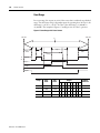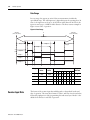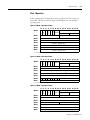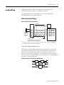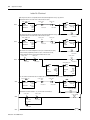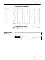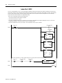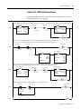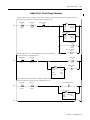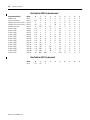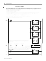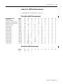
1
Multi-Channel High Speed Counter Module (Catalog Number 1746-HSCE2) User Manual Important User Information Because of the variety of uses for the products described in this publication, those responsible for the application and use of this control equipment must satisfy themselves that all necessary steps have been taken to assure that each application and use meets all performance and safety requirements, including any applicable laws, regulations, codes and standards. The illustrations, charts, sample programs and layout examples shown in this guide are intended solely for purposes of example. Since there are many variables and requirements associated with any particular installation, Rockwell International Corporation does not assume responsibility or liability (to include intellectual property liability) for actual use based upon the examples shown in this publication. Rockwell Automation publication SGI-1.1, Safety Guidelines for the Application, Installation and Maintenance of Solid-State Control (available from your local Rockwell Automation office), describes some important differences between solid-state equipment and electromechanical devices that should be taken into consideration when applying products such as those described in this publication. Reproduction of the contents of this copyrighted publication, in whole or part, without written permission of Rockwell Automation, is prohibited. Throughout this manual we use notes to make you aware of safety considerations: ATTENTION Identifies information about practices or circumstances that can lead to personal injury or death, property damage or economic loss Attention statements help you to: • identify a hazard • avoid a hazard • recognize the consequences IMPORTANT Identifies information that is critical for successful application and understanding of the product. PLC-5 is a registered trademark of Rockwell Automation. SLC, SLC 500, SLC 5/01, SLC 5/02, SLC 5/03, SLC 5/04, and SLC 5/05 are trademarks of Rockwell Automation. RSLogix 500 is a trademark of Rockwell Software, Inc. Summary of Changes The information below summarizes the changes to this manual since the last printing. To help you find new information and updated information in this release of the manual, we have included change bars as shown to the right of this paragraph. New Information i The table below lists sections that include new information. For this new information See page(s) A comparison of Class 1 and Class 4 1-4 Suggestions for reducing noise 3-4 Calculations for adding a resistor to your system 3-8 and 3-9 Clarification on INT: Interrupt Enable function 4-7 Initialization errors caused by the OTE instruction 5-6 Block transfer using a PLC-5, application example 3 6-10 Soft presets, application example 4 6-15 Changing presets dynamically, application example 5 6-18 Retentive counters, application example 6 6-23 A comparison of 1746-HSCE2 to 1746-HSCE Appendix E Publication 1746-UM002A-US-P Summary of Changes ii Publication 1746-UM002A-US-P Table of Contents Preface Who Should Use This Manual . . . . . . . . . . . . . . . . . . . . . . . . . . . . How to Use This Manual . . . . . . . . . . . . . . . . . . . . . . . . . . . . . . . . Manual Contents . . . . . . . . . . . . . . . . . . . . . . . . . . . . . . . . . . . Related Documentation . . . . . . . . . . . . . . . . . . . . . . . . . . . . . . Conventions Used In This Manual . . . . . . . . . . . . . . . . . . . . . . . . . Rockwell Automation Support . . . . . . . . . . . . . . . . . . . . . . . . . . . . Local Product Support . . . . . . . . . . . . . . . . . . . . . . . . . . . . . . . Technical Product Assistance. . . . . . . . . . . . . . . . . . . . . . . . . . . Your Questions or Comments on the Manual . . . . . . . . . . . . . . P-1 P-2 P-2 P-3 P-3 P-4 P-4 P-4 P-4 Chapter 1 Module Overview Multi-Channel High-Speed Counter Module Overview . . . . . . . . . Counters . . . . . . . . . . . . . . . . . . . . . . . . . . . . . . . . . . . . . . . . . . Inputs . . . . . . . . . . . . . . . . . . . . . . . . . . . . . . . . . . . . . . . . . . . . Outputs. . . . . . . . . . . . . . . . . . . . . . . . . . . . . . . . . . . . . . . . . . . Operation . . . . . . . . . . . . . . . . . . . . . . . . . . . . . . . . . . . . . . . . . Operating Class. . . . . . . . . . . . . . . . . . . . . . . . . . . . . . . . . . . . . . . . Class 1. . . . . . . . . . . . . . . . . . . . . . . . . . . . . . . . . . . . . . . . . . . . Class 4. . . . . . . . . . . . . . . . . . . . . . . . . . . . . . . . . . . . . . . . . . . . Class 1 vs Class 4 Comparison . . . . . . . . . . . . . . . . . . . . . . . . . Hardware Features . . . . . . . . . . . . . . . . . . . . . . . . . . . . . . . . . . . . . LEDs. . . . . . . . . . . . . . . . . . . . . . . . . . . . . . . . . . . . . . . . . . . . . Jumpers. . . . . . . . . . . . . . . . . . . . . . . . . . . . . . . . . . . . . . . . . . . 1-1 1-1 1-2 1-2 1-2 1-4 1-4 1-4 1-4 1-5 1-5 1-6 Chapter 2 Module Operation i Operating Modes . . . . . . . . . . . . . . . . . . . . . . . . . . . . . . . . . . . . . . Input Configurations . . . . . . . . . . . . . . . . . . . . . . . . . . . . . . . . . . . Pulse/External Direction . . . . . . . . . . . . . . . . . . . . . . . . . . . . . . Pulse/Internal Direction . . . . . . . . . . . . . . . . . . . . . . . . . . . . . . Up and Down Pulses. . . . . . . . . . . . . . . . . . . . . . . . . . . . . . . . . X1 Quadrature Encoder . . . . . . . . . . . . . . . . . . . . . . . . . . . . . . X2 Quadrature Encoder . . . . . . . . . . . . . . . . . . . . . . . . . . . . . . X4 Quadrature Encoder . . . . . . . . . . . . . . . . . . . . . . . . . . . . . . Input Frequency . . . . . . . . . . . . . . . . . . . . . . . . . . . . . . . . . . . . . . . Gate/Preset Modes . . . . . . . . . . . . . . . . . . . . . . . . . . . . . . . . . . . . . No Preset . . . . . . . . . . . . . . . . . . . . . . . . . . . . . . . . . . . . . . . . . Soft Preset Only . . . . . . . . . . . . . . . . . . . . . . . . . . . . . . . . . . . . Store/Continue . . . . . . . . . . . . . . . . . . . . . . . . . . . . . . . . . . . . . Store/Hold/Resume. . . . . . . . . . . . . . . . . . . . . . . . . . . . . . . . . . Store/Preset/Hold/Resume . . . . . . . . . . . . . . . . . . . . . . . . . . . . Store/Preset/Start . . . . . . . . . . . . . . . . . . . . . . . . . . . . . . . . . . . Gate and Preset Limitations . . . . . . . . . . . . . . . . . . . . . . . . . . . Gate and Preset Considerations. . . . . . . . . . . . . . . . . . . . . . . . . 2-1 2-2 2-2 2-2 2-3 2-3 2-3 2-4 2-4 2-5 2-5 2-5 2-5 2-5 2-6 2-6 2-6 2-6 Publication 1746-UM002A-US-P Table of Contents ii Summary of Available Counter Configurations. . . . . . . . . . . . . . . . 2-7 Counter Types . . . . . . . . . . . . . . . . . . . . . . . . . . . . . . . . . . . . . . . . 2-7 Linear Counter . . . . . . . . . . . . . . . . . . . . . . . . . . . . . . . . . . . . . 2-7 Ring Counter . . . . . . . . . . . . . . . . . . . . . . . . . . . . . . . . . . . . . . 2-8 Rate Value . . . . . . . . . . . . . . . . . . . . . . . . . . . . . . . . . . . . . . . . . . . 2-8 Accuracy . . . . . . . . . . . . . . . . . . . . . . . . . . . . . . . . . . . . . . . . . . 2-9 Output Control . . . . . . . . . . . . . . . . . . . . . . . . . . . . . . . . . . . . . . . 2-9 Range Control . . . . . . . . . . . . . . . . . . . . . . . . . . . . . . . . . . . . . . . . 2-9 Count Range. . . . . . . . . . . . . . . . . . . . . . . . . . . . . . . . . . . . . . 2-10 Rate Range . . . . . . . . . . . . . . . . . . . . . . . . . . . . . . . . . . . . . . . 2-12 Counter Input Data . . . . . . . . . . . . . . . . . . . . . . . . . . . . . . . . . . . 2-12 Class 1 Operation . . . . . . . . . . . . . . . . . . . . . . . . . . . . . . . . . . 2-13 Class 4 Operation . . . . . . . . . . . . . . . . . . . . . . . . . . . . . . . . . . 2-14 Input Word Bit Values . . . . . . . . . . . . . . . . . . . . . . . . . . . . . . 2-15 Output State Byte . . . . . . . . . . . . . . . . . . . . . . . . . . . . . . . . . . 2-16 Counter Status Bytes. . . . . . . . . . . . . . . . . . . . . . . . . . . . . . . . 2-16 Chapter 3 Installation and Wiring Compliance to European Union Directives. . . . . . . . . . . . . . . . . . . EMC Directive . . . . . . . . . . . . . . . . . . . . . . . . . . . . . . . . . . . . . Low Voltage Directive . . . . . . . . . . . . . . . . . . . . . . . . . . . . . . . Prevent Electrostatic Discharge . . . . . . . . . . . . . . . . . . . . . . . . . . . . Setting the Jumpers. . . . . . . . . . . . . . . . . . . . . . . . . . . . . . . . . . . . . Installing the Module . . . . . . . . . . . . . . . . . . . . . . . . . . . . . . . . . . . Important Wiring Considerations. . . . . . . . . . . . . . . . . . . . . . . . . . Considerations for Reducing Noise. . . . . . . . . . . . . . . . . . . . . . Electronic Protection . . . . . . . . . . . . . . . . . . . . . . . . . . . . . . . . . . . Auto Reset Operation . . . . . . . . . . . . . . . . . . . . . . . . . . . . . . . . Input and Output Connections . . . . . . . . . . . . . . . . . . . . . . . . . . . Removing the Terminal Block . . . . . . . . . . . . . . . . . . . . . . . . . Encoder Wiring . . . . . . . . . . . . . . . . . . . . . . . . . . . . . . . . . . . . . . . Differential Encoder Wiring . . . . . . . . . . . . . . . . . . . . . . . . . . . Single-Ended Encoder Wiring (Open Collector). . . . . . . . . . . . Single-Ended Wiring (Discrete Devices) . . . . . . . . . . . . . . . . . . 3-1 3-1 3-1 3-2 3-2 3-3 3-4 3-4 3-5 3-5 3-6 3-6 3-7 3-7 3-8 3-9 Chapter 4 Configuration and Programming Publication 1746-UM002A-US-P Selecting Operating Class . . . . . . . . . . . . . . . . . . . . . . . . . . . . . . . . Power-up Reset . . . . . . . . . . . . . . . . . . . . . . . . . . . . . . . . . . . . . . . . Module Programming. . . . . . . . . . . . . . . . . . . . . . . . . . . . . . . . . . . Programming Cycle . . . . . . . . . . . . . . . . . . . . . . . . . . . . . . . . . Data Format . . . . . . . . . . . . . . . . . . . . . . . . . . . . . . . . . . . . . . . 4-1 4-1 4-1 4-2 4-2 Table of Contents iii Module Setup Block . . . . . . . . . . . . . . . . . . . . . . . . . . . . . . . . . . . . 4-6 Programming Block Identification Bit. . . . . . . . . . . . . . . . . . . . 4-6 TRMT: Transmit Bit . . . . . . . . . . . . . . . . . . . . . . . . . . . . . . . . 4-6 DEBUG: Debug Mode Selection Bit . . . . . . . . . . . . . . . . . . . . 4-6 INT: Interrupt Enable. . . . . . . . . . . . . . . . . . . . . . . . . . . . . . . . 4-7 RVF: Rate Value Format. . . . . . . . . . . . . . . . . . . . . . . . . . . . . . 4-7 PRA: Program Range Allocation . . . . . . . . . . . . . . . . . . . . . . . 4-7 Op Mode: Operating Mode . . . . . . . . . . . . . . . . . . . . . . . . . . . 4-8 Range Allocation Values . . . . . . . . . . . . . . . . . . . . . . . . . . . . . . 4-8 Range Allocation Examples . . . . . . . . . . . . . . . . . . . . . . . . . . . . 4-9 Counter Configuration Block . . . . . . . . . . . . . . . . . . . . . . . . . . . . 4-10 Programming Block Identification Bit. . . . . . . . . . . . . . . . . . . 4-10 TRMT: Transmit Bit . . . . . . . . . . . . . . . . . . . . . . . . . . . . . . . 4-10 DEBUG: Debug Mode Selection Bit . . . . . . . . . . . . . . . . . . . 4-11 PGMn: Program Counter Number Bits . . . . . . . . . . . . . . . . . 4-11 CType: Counter Type Bit . . . . . . . . . . . . . . . . . . . . . . . . . . . 4-11 Input Config: Input Configuration Bits . . . . . . . . . . . . . . . . . 4-11 G/P Mode: Gate/Preset Mode Bits . . . . . . . . . . . . . . . . . . . . . 4-12 Minimum/Maximum Count Value Block. . . . . . . . . . . . . . . . . . . 4-12 Programming Block Identification Bit. . . . . . . . . . . . . . . . . . . 4-13 TRMT: Transmit Bit . . . . . . . . . . . . . . . . . . . . . . . . . . . . . . . 4-13 DEBUG: Debug Mode Selection Bit . . . . . . . . . . . . . . . . . . . 4-13 AUTO PRESET: Automatic Preset Bit . . . . . . . . . . . . . . . . . . 4-13 CNTR No.: Counter Number Bits . . . . . . . . . . . . . . . . . . . . 4-14 Preset Value . . . . . . . . . . . . . . . . . . . . . . . . . . . . . . . . . . . . . . 4-14 Minimum/Maximum Count Value Words . . . . . . . . . . . . . . . 4-14 Counter Type . . . . . . . . . . . . . . . . . . . . . . . . . . . . . . . . . . . . . 4-15 Minimum/Maximum Rate Value Block . . . . . . . . . . . . . . . . . . . . 4-15 Programming Block Identification Bit. . . . . . . . . . . . . . . . . . . 4-16 TRMT: Transmit Bit . . . . . . . . . . . . . . . . . . . . . . . . . . . . . . . 4-16 DEBUG: Debug Mode Selection Bit . . . . . . . . . . . . . . . . . . . 4-16 CNTR No.: Counter Number Bits . . . . . . . . . . . . . . . . . . . . 4-16 Minimum/Maximum Rate Value Words . . . . . . . . . . . . . . . . 4-16 Operating Class. . . . . . . . . . . . . . . . . . . . . . . . . . . . . . . . . . . . 4-17 Program Ranges Block . . . . . . . . . . . . . . . . . . . . . . . . . . . . . . . . . 4-17 Programming Block Identification Bit. . . . . . . . . . . . . . . . . . . 4-18 TRMT: Transmit Bit . . . . . . . . . . . . . . . . . . . . . . . . . . . . . . . 4-18 DEBUG: Debug Mode Selection Bit . . . . . . . . . . . . . . . . . . . 4-18 CNTR No.: Counter Number Bits . . . . . . . . . . . . . . . . . . . . 4-18 Rtype: Range Type. . . . . . . . . . . . . . . . . . . . . . . . . . . . . . . . . 4-19 Range No.: Range Number Bits . . . . . . . . . . . . . . . . . . . . . . . 4-19 Range Start Value, Range Stop Value . . . . . . . . . . . . . . . . . . . 4-20 Output State: Output State Byte . . . . . . . . . . . . . . . . . . . . . . . 4-20 Publication 1746-UM002A-US-P Table of Contents iv Counter Control Block . . . . . . . . . . . . . . . . . . . . . . . . . . . . . . . . . Transmit Bit . . . . . . . . . . . . . . . . . . . . . . . . . . . . . . . . . . . . . . Programming Block Identification Bit . . . . . . . . . . . . . . . . . . Control Words . . . . . . . . . . . . . . . . . . . . . . . . . . . . . . . . . . . . ENn: Enable Counter (n) Bit. . . . . . . . . . . . . . . . . . . . . . . . . SPn: Soft Preset Only (n) Bit . . . . . . . . . . . . . . . . . . . . . . . . . IDn: Internal Direction (n) Bit . . . . . . . . . . . . . . . . . . . . . . . . C/R(n): Count or Rate Value Bit . . . . . . . . . . . . . . . . . . . . . . P(n): Program Counter (n) Bit. . . . . . . . . . . . . . . . . . . . . . . . Output ON (OR) Mask . . . . . . . . . . . . . . . . . . . . . . . . . . . . . Output OFF (AND) Mask . . . . . . . . . . . . . . . . . . . . . . . . . . . Enable Range . . . . . . . . . . . . . . . . . . . . . . . . . . . . . . . . . . . . . Determining Actual Output State. . . . . . . . . . . . . . . . . . . . . . Programming Block Default Values . . . . . . . . . . . . . . . . . . . . . . . Class 1 . . . . . . . . . . . . . . . . . . . . . . . . . . . . . . . . . . . . . . . . . . Class 4 . . . . . . . . . . . . . . . . . . . . . . . . . . . . . . . . . . . . . . . . . . 4-20 4-21 4-21 4-21 4-22 4-22 4-22 4-23 4-23 4-23 4-23 4-24 4-24 4-25 4-25 4-27 Chapter 5 Start Up, Operation, Troubleshooting, and Debug Mode Start Up . . . . . . . . . . . . . . . . . . . . . . . . . . . . . . . . . . . . . . . . . . . . . Normal Operation . . . . . . . . . . . . . . . . . . . . . . . . . . . . . . . . . . . . . Troubleshooting . . . . . . . . . . . . . . . . . . . . . . . . . . . . . . . . . . . . . . . Module Diagnostic Errors. . . . . . . . . . . . . . . . . . . . . . . . . . . . . Module Programming Errors . . . . . . . . . . . . . . . . . . . . . . . . . . Application Errors. . . . . . . . . . . . . . . . . . . . . . . . . . . . . . . . . . . Debug Mode Operation . . . . . . . . . . . . . . . . . . . . . . . . . . . . . . . . . Activating Debug Mode . . . . . . . . . . . . . . . . . . . . . . . . . . . . . . 5-1 5-2 5-2 5-3 5-3 5-4 5-7 5-7 Chapter 6 Application Examples Publication 1746-UM002A-US-P Example 1 - Direct Addressing . . . . . . . . . . . . . . . . . . . . . . . . . . . . 6-2 Ladder File 8 - HSCE2 . . . . . . . . . . . . . . . . . . . . . . . . . . . . . . . 6-2 Ladder File 9 - HSCE2 Initialization Routine. . . . . . . . . . . . . . 6-3 Data Table for N10 File (hexidecimal) . . . . . . . . . . . . . . . . . . . 6-7 Data Table for N11 File (decimal) . . . . . . . . . . . . . . . . . . . . . . 6-7 Example 2 - Indirect Addressing . . . . . . . . . . . . . . . . . . . . . . . . . . . 6-7 Ladder File 8 - HSCE2 . . . . . . . . . . . . . . . . . . . . . . . . . . . . . . . 6-8 Ladder File 9 - HSCE2 Initialization Routine. . . . . . . . . . . . . . 6-9 Data Table for N10 File (hexidecimal) . . . . . . . . . . . . . . . . . . 6-10 Data Table for N11 File (decimal) . . . . . . . . . . . . . . . . . . . . . 6-10 Example 3 - Block Transfers . . . . . . . . . . . . . . . . . . . . . . . . . . . . . 6-10 Ladder File 8 - HSCE2 . . . . . . . . . . . . . . . . . . . . . . . . . . . . . . 6-11 Ladder File 9 - HSCE2 Initialization Routine. . . . . . . . . . . . . 6-13 Data Table for N10 File (hexidecimal) . . . . . . . . . . . . . . . . . . 6-14 Data Table for N11 File (decimal) . . . . . . . . . . . . . . . . . . . . . 6-14 Table of Contents Example 4 - Using Soft Presets . . . . . . . . . . . . . . . . . . . . . . . . . . . Ladder File 8 - HSCE2 . . . . . . . . . . . . . . . . . . . . . . . . . . . . . . Ladder File 9 - HSCE2 Initialization Routine . . . . . . . . . . . . . Data Table for N10 File (hexidecimal) . . . . . . . . . . . . . . . . . . Data Table for N11 File (decimal) . . . . . . . . . . . . . . . . . . . . . Example 5 - Change Presets Dynamically . . . . . . . . . . . . . . . . . . . Ladder File 8 - HSCE2 . . . . . . . . . . . . . . . . . . . . . . . . . . . . . . Ladder File 9 - HSCE2 Initialization Routine . . . . . . . . . . . . . Ladder File 14 - Preset Change Subroutine . . . . . . . . . . . . . . . Data Table for N10 File (hexidecimal) . . . . . . . . . . . . . . . . . . Data Table for N11 File (decimal) . . . . . . . . . . . . . . . . . . . . . Example 6 - Retentive Counters . . . . . . . . . . . . . . . . . . . . . . . . . . Ladder File 8 - HSCE2 . . . . . . . . . . . . . . . . . . . . . . . . . . . . . . Ladder File 9 - HSCE2 Initialization Routine . . . . . . . . . . . . . Data Table for N10 File (hexidecimal) . . . . . . . . . . . . . . . . . . Data Table for N11 File (decimal) . . . . . . . . . . . . . . . . . . . . . v 6-15 6-16 6-17 6-18 6-18 6-18 6-19 6-20 6-21 6-22 6-22 6-23 6-24 6-25 6-25 6-25 Appendix A Specifications General . . . . . . . . . . . . . . . . . . . . . . . . . . . . . . . . . . . . . . . . . . . . . . A-1 Inputs A, B, and Z . . . . . . . . . . . . . . . . . . . . . . . . . . . . . . . . . . . . . A-1 Outputs (sourcing) . . . . . . . . . . . . . . . . . . . . . . . . . . . . . . . . . . . . . A-2 On-State Current Derating . . . . . . . . . . . . . . . . . . . . . . . . . . . . A-2 Throughput and Timing . . . . . . . . . . . . . . . . . . . . . . . . . . . . . . . . . A-3 Appendix B Connecting a Differential Encoder Appendix C Module Programming Quick Reference Appendix D Frequently Asked Questions Appendix E Comparing 1746-HSCE2 to 1746-HSCE Glossary Index Publication 1746-UM002A-US-P Table of Contents vi Publication 1746-UM002A-US-P Preface Read this preface to familiarize yourself with the rest of the manual. This preface covers the following topics: • who should use this manual • how to use this manual • related publications • conventions used in this manual • Rockwell Automation support Who Should Use This Manual Use this manual if you are responsible for designing, installing, programming, or troubleshooting control systems that use Allen-Bradley small logic controllers. You should have a basic understanding of SLC 500™ products. You should understand programmable controllers and be able to interpret the ladder logic instructions required to control your application. If you do not, contact your local Rockwell Automation representative for information on available training courses before using this product. 1 Publication 1746-UM002A-US-P P-2 How to Use This Manual As much as possible, we organized this manual to explain, in a task-by-task manner, how to install, configure, program, operate and troubleshoot an SLC 500-based system using the 1746-HSCE2 module. Manual Contents If you want... See A description of the purpose and scope of this manual, as well as references to related publications Preface An overview of the 1746-HSCE2 module Chapter 1 A description of module operation, including operating modes and input configurations Chapter 2 Information on module installation, input and output wiring, terminal block removal, Chapter 3 and wiring diagrams Publication 1746-UM002A-US-P Instructions on how to configure the module and descriptions of programming parameters Chapter 4 A description of module start-up, normal operation, troubleshooting, and debug mode operation Chapter 5 Application examples Chapter 6 Specifications for temperature, humidity, input, output, and voltage Appendix A Information on connecting a differential encoder to the multi-channel high-speed counter module Appendix B A quick reference to the 1746-HSCE2 module programming blocks Appendix C Answers to frequently asked questions about the 1746-HSCE2 module Appendix D A comparison of the 1746-HSCE2 to the 1746-HSCE. Appendix E Definitions of terms used in this manual Glossary P-3 Related Documentation The table below provides a listing of publications that contain important information about SLC™ products. For Read this document Document number A reference manual containing status file data, instruction set, and troubleshooting information SLC 500™ and MicroLogix™ 1000 Instruction Set Reference Manual 1747-6.15 A description of how to install and use your Modular SLC 500 programmable controller SLC 500™ Modular Hardware Style Installation and Operation Manual 1747-6.2 An overview of the SLC 500™ family of products SLC 500 System Overview 1747-SO001B-US-P A CD-ROM containing a collection of SLC 500 user and reference manuals. SLC 500™ Literature Collections 1747-CD1-1 A procedural and reference manual for technical personnel who use Hand-Held Terminal User Manual an HHT to develop control applications 1747-NP002 An introduction to HHT for first-time users, focusing on simple tasks Getting Started Guide for HHT and exercises to allow the user to begin programming in the shortest possible time 1747-NM009 In-depth information on grounding and wiring Allen-Bradley programmable controllers 1770-4.1 Allen-Bradley Programmable Controller Grounding and Wiring Guidelines Application Considerations for A description of important differences between solid-state programmable controller products and hard-wired electromechanical Solid-State Controls devices SGI-1.1 An article on wire sizes and types for grounding electrical equipment National Electrical Code Published by the National Fire Protection Association of Boston, MA A glossary of industrial automation terms and abbreviations AG-7.1 Allen-Bradley Industrial Automation Glossary If you would like a manual, you can: • download a free electronic version from the internet at www.theautomationbookstore.com • purchase a printed manual by: – contacting your local distributor or Rockwell Automation representative – visiting www.theautomationbookstore.com and placing your order – calling 1.800.963.9548 (USA/Canada) or 001.330.725.1574 (Outside USA/Canada) Conventions Used In This Manual The following conventions are used throughout this manual: • Bulleted lists (like this one) provide information, not procedural steps. • Numbered lists provide sequential steps or hierarchical information. • Italic type is used for emphasis. • Text in this font indicates words or phrases you should type. Publication 1746-UM002A-US-P P-4 Rockwell Automation Support Rockwell Automation offers support services worldwide, with over 75 Sales/ Support Offices, 512 authorized distributors and 260 authorized Systems Integrators located throughout the United States alone, plus Rockwell Automation representatives in every major country in the world. Local Product Support Contact your local Rockwell Automation representative for: • sales and order support • product technical training • warranty support • support service agreement Technical Product Assistance If you need to contact Rockwell Automation for technical assistance, please review the Troubleshooting section of Chapter 5 first. Then call your local Rockwell Automation representative. Your Questions or Comments on the Manual If you find a problem with this manual, please notify us. If you have any suggestions for how this manual could be made more useful to you, please contact us at the address below: Rockwell Automation Control and Information Group Technical Communication, Dept. A602V P.O. Box 2086 Milwaukee, WI 53201-2086 Publication 1746-UM002A-US-P Chapter 1 Module Overview This chapter contains the following: • multi-channel high-speed counter module overview • operating class • hardware features Multi-Channel High-Speed Counter Module Overview The 1746-HSCE2 is an intelligent counter module with its own microprocessor and I/O that is capable of reacting to high-speed input signals without the intervention of the SLC processor. The module is compatible with the SLC 500 family and can be used in a remote chassis with the SLC Remote I/O Adapter Module (1747-ASB). Counters The module is able to count in either direction. A maximum of four pulse counters are available (or 2 quadrature counters). Each counter can count to +/- 8,388,607 as a ring or linear counter. In addition to providing a count value, the module provides a rate value up to +/-1 MHz, dependent on the type of input. The rate value is the input frequency (in Hertz) to the counter. When the count value is increasing, the rate value is positive. When the count value is decreasing, the rate value is negative. Counters can also be preset to any value between the minimum and maximum values. The conditions that preset the count value and generate capture values are configured by the gate/preset modes. The four counters can have different gate/ preset modes. 1 Publication 1746-UM002A-US-P 1-2 Module Overview Inputs The module features six high-speed differential inputs labeled ±A1, ±B1, ±Z1, ±A2, ±B2, and ±Z2. It supports quadrature encoders with ABZ inputs and/or up to six discrete switches. In addition, x1, x2, and x4 counting configurations are provided to fully use the capabilities of high resolution quadrature encoders. The inputs can be wired for single-ended or differential use. Inputs are opto-isolated from the backplane. Outputs Eight outputs are available, four real (dc sourcing) and four virtual bits. The virtual outputs are available to the processor only. The real outputs are protected from overloads by a self-resetting fuse. The outputs can be controlled by any or all of the counters and/or directly controlled by the user’s program. Up to 16 dynamically configurable ranges are available, using rates or counts to control outputs. The ranges, programmed with range start and range stop values, can overlap. If the count or rate is within more than one range, the output patterns of those ranges are combined (logically ORed) to determine the actual status of the output. When an output is enabled by more than one counter and/or with the user program, its output state is determined by logically ORing the programmed setpoints of all those counters and the user program. Operation Module operation is controlled by user-programmed settings in the following six module programming blocks. • Module Setup Block • Counter Configuration Block • Minimum/Maximum Count Value Block • Minimum/Maximum Rate Value Block • Program Ranges Block • Counter Control Block Publication 1746-UM002A-US-P Module Overview 1-3 Most programming parameters, except those in the Module Setup and Counter Configuration blocks, are dynamic and can be changed without halting counter operation. The table below lists the static and dynamic parameters by programming block. Programming Block Parameter Type(1) Operating Mode Module Setup Range Allocation Interrupt Enable Static Rate Value Format Counter Type Counter Configuration Input Configuration Static(2) Gate/Preset Mode Min./Max. Count Value Min./Max. Rate Value Minimum Count Static(2) Maximum Count Static(2) Preset Value Dynamic(3) Minimum Rate Maximum Rate Dynamic Counter Number Range Type Program Range Range Number Start Value Dynamic Stop Value Output Image Enabled Soft Preset Only Internal Direction Counter Control Output ON Mask Dynamic Output OFF Mask Count or Rate Value Range Enable Mask (1) STATIC = the associated counter must be disabled to set this parameter. DYNAMIC = this parameter may be changed while the associated counter is running. (2) Only the selected counter must be disabled. (3) Under specific conditions, this parameter is dynamic. See page 4-14 for more information. Publication 1746-UM002A-US-P 1-4 Module Overview Operating Class Module operation differs slightly based on the operating class. The operating class is selected via the module ID code. Class 1 Class 1 operation is compatible with all SLC 500 processors. In Class 1 operation, the module uses 8 input and 8 output words and has an associated ID code of 3511. A maximum of four 16-bit counters are available in this operating class. Class 4 Class 4 operation is compatible with SLC 5/03 and above systems. In Class 4 operation, the module uses 23 input and 8 output words and has an associated ID code of 15912. A maximum of four 24-bit counters are available in this class. Class 1 vs Class 4 Comparison Publication 1746-UM002A-US-P Class Class 1 Class 4 Counters 16-bit (±32,767) 24-bit (±8,388,607) Input Words 8 with limited information. 23 with all information. Backplane Interrupts Not permitted. Permitted. Use in RIO Chassis Permitted. Not permitted. Use in ControlNet Chassis Not permitted. Permitted. Module ID Code 3511 15912 Module Overview Hardware Features 1-5 The module’s hardware features are illustrated below. Refer to Chapter 3 for detailed information on installation and wiring. Figure 1.1 Hardware Features COUNTER OUTPUT STATUS Input Status LEDs 0 1 2 A1 B1 Z1 RUN A2 B2 Z2 FLT Output Status LEDs 3 INPUT STATUS Running Status LED Fault Status LED HSCE2 Input and Output Terminals LEDs The front panel has a total of twelve indicator LEDs, as shown in Figure 1.1 on page 1-5. LED Color Indicates 0 OUT Green ON/OFF status of real output 1 OUT Green ON/OFF status of real output 2 OUT Green ON/OFF status of real output 3 OUT Green ON/OFF status of real output RUN Green Running status of the module FLT Red Steady on: Module fault Flashing: Output overcurrent A1 Yellow ON/OFF status of input A1 A2 Yellow ON/OFF status of input A2 B1 Yellow ON/OFF status of input B1 B2 Yellow ON/OFF status of input B2 Z1 Yellow ON/OFF status of input Z1 Z2 Yellow ON/OFF status of input Z2 Publication 1746-UM002A-US-P 1-6 Module Overview Jumpers Six jumpers select the input voltages for the six inputs A1, B1, Z1, A2, B2, and Z2. The module accepts input voltages of 5V dc, 12V dc, or 24V dc. See Chapter 3 for jumper locations and settings. Publication 1746-UM002A-US-P Chapter 2 Module Operation The chapter contains information about: • operating modes • input configurations • gate/preset modes • counter types • rate value • outputs • range types Operating Modes The module’s operating mode determines the number of available counters and which inputs are attached to them. The three operating modes and their input assignments are summarized in Figure 2.1. Figure 2.1 Operating Mode Input Assignments A1 B1 A1 Counter 1 Counter 3 B1 Z1 A2 B2 Counter 1 Counter 3 B2 Z1 Counter 2 A2 Counter 4 Z2 Counter 2 Counter 4 Z2 Operating Mode 1 Operating Mode 2 A1 Counter 1 Counter 3 B2 Counter 2 Counter 4 B1 Z1 A2 Z2 Operating Mode 3 1 Publication 1746-UM002A-US-P 2-2 Module Operation Input Configurations Input configurations determine how the A and B inputs cause the counter to increment or decrement. The six available configurations are: • Pulse/External Direction • Pulse/Internal Direction • Up and Down Pulses • X1 Quadrature Encoder • X2 Quadrature Encoder • X4 Quadrature Encoder See the Summary of Available Counter Configurations on page 2-7 for the input configurations available for the counters, based on operating mode. Pulse/External Direction With this configuration, the B input controls the direction of the counter, as shown below. If the B input is low (0), the counter increments on the rising edges of input A. If the input B is high (1), the counter decrements on the rising edges of input A. Figure 2.2 Pulse/External Direction Configuration Count Pulse Encoder or Sensor Input A Direction Control Input B Input Z Sensor or Switch Count Pulse Direction Control High = Decrement Low = Increment Count 1 2 3 2 1 0 1 2 Pulse/Internal Direction When the Pulse/Internal Direction configuration is selected, a bit written from the backplane determines the direction of the counter. The counter increments on the rising edge of the input if the bit is low (0) and decrements on the rising edge of the input if the bit is high (1). Publication 1746-UM002A-US-P Module Operation 2-3 Up and Down Pulses In this configuration, the counter increments on the rising edge of pulses applied to input A and decrements on the rising edge of pulses applied to input B. NOTE When both inputs transition simultaneously or near simultaneously, the net result is no change to the count value. Therefore, simultaneous (or near simultaneous) pulses are ignored and no change in the count value is reported. Figure 2.3 Up and Down Pulse Configuration Input A Increment Pulse (count up) Incrementing Encoder or Sensor Input B Input Z Decrementing Encoder or Sensor Decrement Pulse (count down) Module Increment Pulse (Input A) Decrement Pulse (Input B) Count 1 2 3 2 1 0 1 2 X1 Quadrature Encoder When a quadrature encoder is attached to inputs A and B, the count direction is determined by the phase angle between inputs A and B. If A leads B, the counter increments. If B leads A, the counter decrements. The counter changes value only on one edge of input A as shown in Figure 2.4 on page 2-4. NOTE If B is low, the count increments on the rising edge of input A and decrements on the falling edge of input A. If B is high, all transitions on input A are ignored. X2 Quadrature Encoder Like the X1 Quadrature Encoder, the count direction is determined by the phase angle between inputs A and B. If A leads B, the counter increments. If B leads A, the counter decrements. However, the counter changes value on the rising and falling edges of input A, as shown in Figure 2.4 on page 2-4. Publication 1746-UM002A-US-P 2-4 Module Operation X4 Quadrature Encoder Operation is similar to the X2 Quadrature Encoder configuration, except the counter changes value on the rising and falling edges of inputs A and B as shown in Figure 2.4. Figure 2.4 Quadrature Encoder Configurations A Input A B Input B Z Quadrature Encoder Input Z Reverse Rotation Forward Rotation A B 1 2 3 2 1 0 X1 Count 1 2 3 4 5 6 5 4 3 2 1 0 X2 Count 1 2 3 4 5 6 7 8 9 10 11 12 11 10 9 8 7 6 5 4 3 2 1 X4 Count IMPORTANT The input configuration is limited by the operating mode. In mode 1, Counters 1 and 2 can be assigned any input configuration. In mode 2, Counter 1 can be assigned any configuration, but Counters 2 and 3 are configured as pulse/ internal direction. In mode 3, all counters have the pulse/ internal direction configuration. See the Summary of Available Counter Configurations on page 2-7. Input Frequency Input frequency is determined by the input configuration as shown in the table below. Input Configuration Input Frequency X4 Quadrature Encoder 250 kHz X2 Quadrature Encoder 500 kHz All Other Configurations 1 MHz IMPORTANT The minimum high and low times for the pulse train are 475 ns. Therefore, the input pulse train must fall between a 47.5 to 52.5 percent duty cycle at 1 MHz. Publication 1746-UM002A-US-P 0 Module Operation Gate/Preset Modes 2-5 A counter’s gate/preset mode determines what, if any, gating is applied to the counter and what, if any, conditions will preset the counter to the preset value. The Z inputs are the only inputs used for gating or presetting. The six gate/preset modes are described below. No Preset The counter is not preset under any conditions. The Z inputs are not used. Soft Preset Only The counter is preset when the matching preset bit in the SLC 500 output image table experiences a positive transition, but not in response to the Z input. NOTE The soft preset bit operates in all the gate/preset modes except No Preset. Store/Continue store, continue counting The count value is captured when the module detects an inactive-to-active transition on the Z input of the counter. This stored value is made available to the backplane. A stored status bit in the input image table is set to signal the processor that a new value is available. This bit is active until the capture value is read by the processor. Therefore, it is on for a maximum of 10 ms in Class 1, and a maximum of one scan or 10 ms, whichever is shorter, in Class 4. If a second capture event occurs before the first is read, the first value is lost. The count and rate values are not affected by a store event. Store/Hold/Resume counter has stopped counting resume counting stop count store count The count value, captured when the module detects a positive transition on the Z input, is made available to the backplane. A stored status bit is set in the input image table to signal the processor that a new value is available. This bit is active until the capture value is read by the processor. Therefore, it is on for a maximum of 10 ms in Class 1, and a maximum of one scan or 10 ms, whichever is shorter, in Class 4. The count value is held as long as the Z input is active. Because the count value is not changing, the rate value is equal to zero while the counter is held. Publication 1746-UM002A-US-P 2-6 Module Operation Store/Preset/Hold/Resume counter has stopped counting stop count, store count, preset start counting from preset The counter is set to its programmed preset value when the module detects a positive transition on the Z input of the counter. The capture value is made available to the backplane. A stored status bit is set in the input image table to signal the processor that a new value is available. This bit is active until the capture value is read by the processor. Therefore, it is on for a maximum of 10 ms in Class 1, and a maximum of one scan or 10 ms, whichever is shorter, in Class 4. The preset counter value is held as long as the Z input remains active. Because the count value is not changing, the rate value equals zero while the preset value is held. Store/Preset/Start store count, preset, start counting The counter is set to its programmed preset value when the module detects a positive transition on the Z input of the counter. The capture value is made available to the backplane. A stored status bit is set in the input image table to signal the processor that a new value is available.This bit is active until the capture value is read by the processor. Therefore, it is on for a maximum of 10 ms in Class 1, and a maximum of one scan or 10 ms, whichever is shorter, in Class 4. Gate and Preset Limitations Because only the Z inputs are used for external gating and presetting, the only gate/preset modes available for Counters 3 and 4 are No Preset and Soft Preset Only. All six modes are always available for Counters 1 and 2. IMPORTANT In Class 1, Operating Mode 2, Counter 2 does not have a capture value available. In Class 1, Operating Mode 3, no capture values are available. Gate and Preset Considerations Z-pulse Preset Operation In applications where the Z pulse of the encoder is being used to preset the position, and where the Z pulse of the encoder is aligned with either the A or B pulses, the capture or count value may be affected by ± 1 count. If the Z pulse is edge aligned with the A pulse, preset operations may not be performed accurately in any of the quadrature modes. If the Z pulse is edge aligned with the B pulse, preset operation may not be performed accurately in the X4 quadrature mode only. A small capacitor (for example, 0.01 µF) across the Z inputs will dis-align these inputs and should correct this condition. Capture Value Bit Operation In programs exceeding 10 ms scan times, the capture value bit may be reset before it is read into the I/O image at the processor. Publication 1746-UM002A-US-P Module Operation Summary of Available Counter Configurations The table below summarizes the input configurations and gate/preset modes available for all counters, based on operating mode. Operating Mode Counter Input Configuration Gate/Preset Mode 1 1 All All 2 All All 1 All All 2 Pulse/Internal Direction All 3 Pulse/Internal Direction No Preset or Soft Preset Only 1 Pulse/Internal Direction All 2 Pulse/Internal Direction All 3 Pulse/Internal Direction No Preset or Soft Preset Only 4 Pulse/Internal Direction No Preset or Soft Preset Only 2 3 Counter Types 2-7 Each counter can be programmed to operate as a linear or ring counter. Both types are described below. Linear Counter The figure below demonstrates linear counter operation. In linear operation, the count value must remain within the programmed minimum/maximum values. If the count value goes above or below these values, the counter stops counting, and an overflow/underflow bit is set. In the overflow or underflow condition, the rate value continues to be updated and valid. The number of pulses accumulated in an overflow/underflow state are ignored. The counter begins counting again when pulses are applied in the proper direction. For example, if you exceed the maximum by 1,000 counts, you do not need to apply 1,000 counts in the opposite direction before the counter begins counting down. The first pulse in the opposite direction decrements the counter. Figure 2.5 Linear Counter Diagram Minimum Value 0 Maximum Value Count Up Counter Value Count Down Underflow Overflow Publication 1746-UM002A-US-P 2-8 Module Operation Ring Counter Figure 2.6 demonstrates ring counter operation. In ring counter operation, the count value changes between programmable minimum and maximum values. If, when counting up, the counter reaches the maximum value, it rolls over to the minimum value. If, when counting down, the counter reaches the minimum value, it rolls over to the maximum value. Figure 2.6 Ring Counter Diagram Maximum Value Minimum Value Rollover Count Up Count Down Rate Value The rate value reported to the processor is calculated in counts per second (Hz), and is available with all input configurations. The input configuration determines how the rate value is calculated. When the count value is increasing, the rate value is positive. When the count value is decreasing, the rate value is negative. The rate value is generally calculated as follows: When the first input pulse is received, the value of an independent, free-running timer (Ta) is recorded. The module waits approximately 16 ms, while counting more input pulses. After 16 ms, the module waits for the next input pulse, and the value of the independent timer (Tb) is again recorded. The module then calculates the rate value using the formula: number of counts rate value = ---------------------------------------------- Tb – Ta Additional checks ensure that rates below 1 Hz, which are not supported by the module, and frequencies due to motor vibration, are not counted in the rate value calculation. Table 2.1 Typical Rate Update Times Publication 1746-UM002A-US-P Rates (Hz) Time Between Pulses (ms) Time Between Updates (ms) 1 to 59 17 to 1000 17 to 1000 60 to 1000 0 to 16 0 to 33 Above 1000 0 to 1 16 Module Operation 2-9 Accuracy The accuracy of the rate value can be ±0.005% (typical). For this resolution, the rate measurement value must be transferred in single-precision floating-point format. This format is only available when the module operates as Class 4. Fractional rates, those between 1 and 0 or -1 and 0, are not reported. The rate measurement value can also be transferred as an integer value. The integer format is available in both Class 1 and Class 4. Output Control All eight outputs can be controlled by any or all of the counters, or they can be controlled by the user program. When controlled by a counter, an output can be programmed to turn on or off based on the count value and/or rate value of the counter. The eight outputs are divided into four real outputs and four virtual outputs. The outputs can be activated from the user program or from the module in response to specified input events. The status of the real outputs is available to the user program. The virtual outputs are available only to the user program. They have no real output associated with them. The real outputs are protected from overloads by a self-resetting fuse. Range Control The module can be programmed to use either counter or rate ranges to determine whether an output is active. Up to 16 dynamically configurable ranges are available. The ranges, programmed using range start and range stop values, can overlap. When the count is within more than one range, the output patterns of those ranges are combined (logically ORed) to determine the actual status of the output. A mixture of count ranges and rate ranges may be used. Publication 1746-UM002A-US-P 2-10 Module Operation Count Range In a count range, the outputs are active if the count value is within the user-defined range. The valid count range is dependent upon the operating class. In Class 1, the valid range is -32,767 to +32,767. In Class 4, the valid range is -8,388,607 to +8,388,607. The examples in Figure 2.7 and Figure 2.8 use Class 1 operation. Figure 2.7 Count Range with Linear Counter -32,767 Range 4 Stop Value on +32,767 0 Range 2 Range 1 Range 4 Start Value Range 3 Output 0 off Output 1 Output 2 Output 3 Range Start Value Stop Value 1 -7000 2 Outputs(1) 7 6 5 4 3 2 1 0 -5000 0 0 0 0 0 0 0 1 0 -1000 +4500 0 0 0 0 0 0 1 0 1 3 -4000 +3000 0 0 0 0 0 1 0 0 2 4 +9000 -9000 0 0 0 0 1 0 0 1 0 and 3 (1) Bits 0 through 3 are real outputs. Bits 4 through 7 are virtual outputs. Publication 1746-UM002A-US-P Outputs Affected Module Operation 2-11 Figure 2.8 Count Range with Ring Counter Range 3 32,000 500 200 1 Range 2 32,767 23,000 8,000 Range 4 20,000 10,000 12,500 Range Start Value Stop Value 1 10,000 2 Range 1 Outputs(1) Outputs Affected 7 6 5 4 3 2 1 0 12,500 0 0 0 0 0 0 0 1 0 200 8,000 0 0 0 0 0 0 1 0 1 3 32,000 500 0 0 0 0 0 1 0 0 2 4 20,000 23,000 0 0 0 0 1 0 0 1 0 and 3 (1) Bits 0 through 3 are real outputs. Bits 4 through 7 are virtual outputs. Publication 1746-UM002A-US-P 2-12 Module Operation Rate Range In a rate range, the outputs are active if the rate measurement is within the user-defined range. The valid input rate is dependent upon the operating class. In Class 1, the input rate can be up to 32,767 Hz in either direction. In Class 4, the input rate can be up to 1 MHz in either direction. The linear counter example in Figure 2.9 uses Class 1 operation. Figure 2.9 Rate Range -32,767 (min. rate value) 0 +32,767 (max. rate value) Rate Value Range 4 Range 2 Range 1 Range 4 Range 3 on off Output 0 Output 1 Output 2 Output 3 Range Start Value Stop Value 1 -7000 2 Outputs(1) Outputs Affected 7 6 5 4 3 2 1 0 -5000 0 0 0 0 0 0 0 1 0 -1000 +4500 0 0 0 0 0 0 1 0 1 3 -4000 +3000 0 0 0 0 0 1 0 0 2 4 +20000 -20000 0 0 0 0 1 0 0 1 0 and 3 (1) Bits 0 through 3 are real outputs. Bits 4 through 7 are virtual outputs. Counter Input Data Publication 1746-UM002A-US-P The format of the counter input data table depends on the module’s mode and class of operation. The status data formats for Class 1 and Class 4 are shown below, followed by explanations of the programming bits and status bytes. Mode 1 is the default for both Class 1 and Class 4 operation. Module Operation 2-13 Class 1 Operation In this operating class, the input data consists of eight words. The counters are sixteen bits. The data stored in an input word change based on the module’s operating mode. Figure 2.10 Mode 1 Input Data Format Word 1 0 OP MODE FB1 DEBUG PERR ACK Word 0 MFLT 15 14 13 12 11 10 09 08 07 06 05 04 03 02 01 00 Counter 2 Status Output State Virtual Real Counter 1 Status Word 2 Counter 1: Count Value Word 3 Counter 1: Rate Value Word 4 Counter 1: Capture Value(1) Word 5 Counter 2: Count Value Word 6 Counter 2: Rate Value Word 7 Counter 2: Capture Value(1) (1) See page 2-5. for a description of capture values. Figure 2.11 Mode 2 Input Data Format Word 1 0 OP MODE FB1 DEBUG PERR ACK MFLT 15 14 13 12 11 10 09 08 07 06 05 04 03 02 01 00 Word 0 Counter 2: Status Output State Virtual Real Counter 1: Status Word 2 Counter 1: Count Value Word 3 Counter 1: Rate Value Word 4 Counter 1: Capture Value(1) Word 5 Counter 2: Count or Rate Value Word 6 0 0 0 0 Word 7 0 0 0 0 Counter 3: Status Counter 3: Count or Rate Value (1) See page 2-5. for a description of capture values. Figure 2.12 Mode 3 Input Data Format Word 1 0 FB1 DEBUG PERR ACK Word 0 MFLT 15 14 13 12 11 10 09 08 07 06 05 04 03 02 01 00 Counter 2 Status OP MODE Output State Virtual Real Counter 1 Status Word 2 Counter 1: Count or Rate Value Word 3 Counter 2: Count or Rate Value Word 4 Counter 4: Status Counter 3: Status Word 5 Counter 3: Count or Rate Value Word 6 Counter 4: Count or Rate Value Word 7 Not Used. Set equal to 0000H Publication 1746-UM002A-US-P 2-14 Module Operation Class 4 Operation In Class 4 operation, the counter data consist of a maximum of 23 words. Figure 2.13 Class 4 Data Format Word 1 FB1 DEBUG PERR ACK Word 0 MFLT 15 14 13 12 11 10 09 08 07 06 05 04 03 02 01 00 0 Counter 2 Status OP MODE Output State Virtual Real Counter 1 Status Word 2 Upper 4 digits: Counter 1 Count Value Word 3 Lower 3 digits: Counter 1 Count Value Word 4 Counter 1 Rate Value(1) Word 6 Upper 4 digits: Counter 1 Capture Value Word 7 Lower 3 digits: Counter 1 Capture Value Word 8 Upper 4 digits: Counter 2 Count Value Word 9 Lower 3 digits: Counter 2 Count Value Word 10 Counter 2 Rate Value(1) Word 11 Word 12 Upper 4 digits: Counter 2 Capture Value Word 13 Lower 3 digits: Counter 2 Capture Value Word 14 Counter 4 Status Counter 3 Status Word 15 Upper 4 digits: Counter 3 Count Value Word 16 Lower 3 digits: Counter 3 Count Value Word 17 Counter 3 Rate Value(1) Word 18 Word 19 Upper 4 digits: Counter 4 Count Value Word 20 Lower 3 digits: Counter 4 Count Value Word 21 Counter 4 Rate Value(1) Word 22 Transferred in Mode 3(2) Transferred in Modes 2 and 3(2) Transferred in all Modes(2) Word 5 (1) The format of the Rate Values is programmed with the Rate Value Format bit in the Module Setup programming block. This bit specifies the rate value to be in integer or floating-point format. The default is integer format. Count values are always transferred in integer format. See Data Format on page 4-2. (2) Data values transferred. Regardless of operating mode, the module will transfer up to 23 words. Words that do not contain relevant data are set to 0000H. Publication 1746-UM002A-US-P Module Operation 2-15 Input Word Bit Values ACK: Acknowledge Bit This bit makes a 0 to 1 transition to signal the receipt of programming data. MFLT: Module Fault Bit This bit is reset when the module is functioning normally. PERR: Programming Error Bit The state of this bit is valid only when the acknowledge bit is set. This bit is reset when the last programming block is accepted without error. It is set when any one of the reserved bits are set or another programming error has occurred. For a list of other programming error conditions, see Module Programming Errors on page 5-3. DEBUG: Debug Mode Bit This bit is set when the debug mode is active. IMPORTANT When the debug mode is active, the input data file shows the programming setup, not rate and count values. For details, see Debug Mode Operation on page 5-7. FB1: Fuse Status Bit The FB1 fuse status bit is set (1) when the fuse is open. In addition, the module fault LED blinks to indicate an open fuse. When FB1 is set (1), the real outputs do not function. Virtual outputs are not affected. The input word reflects this condition. The module tries resetting the outputs at intervals of 500 ms. During each retry, the fuse status bit is reset (0). After the overload condition is corrected, the fuse bit resets (0) automatically. Publication 1746-UM002A-US-P 2-16 Module Operation OP MODE: Operating Mode Bits The module uses these two bits to tell the processor what mode it is in. In class 1, the data value that an input word contains changes based on the operating mode. Table 2.2 Mode Bit Settings Bit 09 Bit 08 Mode 0 0 Reserved 0 1 Mode 1 1 0 Mode 2 1 1 Mode 3 Output State Byte These bits correspond to the real or virtual state of the outputs. Bits 00 through 03 represent real outputs. Bits 04 through 07 represent virtual outputs. Counter Status Bytes Each counter has an associated status byte. The format of the byte depends on the module’s class of operation as shown below. Figure 2.14 Class 1 Counter Status Byte Format 15 07 C/R 14 06 CapV 13 05 ROvF 12 04 RUdF 11 03 COvF 10 02 CUdF 09 01 09 01 08 00 CState Figure 2.15 Class 4 Counter Status Byte Format Publication 1746-UM002A-US-P 15 07 14 06 13 05 12 04 11 03 10 02 0 CapV ROvF RUdF COvF CUdF 08 00 CState Module Operation 2-17 C/R: Count/Rate Bit The count/rate bit is used only in Class 1 operating mode. Because only one data word is available for Counters 2 and 3 in operating mode 2, and one data word for each of the four counters in operating mode 3, the module transfers either the counter’s count or rate value. When this bit is reset (0), the data in the corresponding word is the count value. When this bit is set (1), the data in the corresponding word is the rate value. CapV: Capture Value Bit This bit is used for Counters 1 and 2 only. When the gate/preset mode is set to Store/Continue, Store/Hold/Resume, Store/Preset/Hold/Resume, or Store/Preset/Start, this bit is set until the capture value is read. The capture value is read as a result of an I/O scan or immediate input instruction. The capture value bit is on for a maximum of 10 ms in Class 1, and a maximum of one scan or 10 ms, whichever is shorter, in Class 4. ROvF: Rate Overflow Bit This bit is set when the rate is greater than the maximum rate value. RUdF: Rate Underflow Bit This bit is set when the rate is less than the minimum rate value. COvF: Counter Overflow Bit When the counter is configured as a linear counter, this bit is set when the count would become one over the maximum count value. NOTE Counter overflow or underflow bits are reset when a pulse in the opposite direction is received. CUdF: Counter Underflow Bit When the counter is configured as a linear counter, this bit is set when the count would become one under the minimum count value. Publication 1746-UM002A-US-P 2-18 Module Operation CState: Counter State Bits These two bits show the operational state of the counter. Table 2.3 Counter State Bit Settings Publication 1746-UM002A-US-P Bits 09 or 01 Bits 08 or 00 Operating State 0 0 Stopped 0 1 Running 1 0 Hold 1 1 Reserved Chapter 3 Installation and Wiring This chapter provides the following information: • compliance to European Union Directives • module installation • wiring considerations • input/output connections • encoder wiring • switch wiring Compliance to European Union Directives If this product has the CE mark, it is approved for installation within the European Union and EEA regions. It has been designed and tested to meet the following directives. EMC Directive This product is tested to meet Council Directive 89/336/EED Electromagnetic Compatibility (EMC) and the following standards, in whole or in part, documented in a technical construction file: EN50081-2 EMC — Generic Emission Standard, Part 2 – Industrial Environment EN50082-2 EMC — Generic Emission Standard, Part 2 – Industrial Environment This product is intended for use in an industrial environment. Low Voltage Directive This product is tested to meet Council Directive 73/23/EEC Low Voltage, by applying the safety requirements of EN 61131-2 Programmable Controllers, Part 2 – Equipment Requirements and Tests. For specific information required by EN61131-2, see the appropriate sections in this publication, as well as the following Allen-Bradley publications: • Industrial Automation, Wiring and Grounding Guidelines for Noise Immunity, publication 1770-4.1 • Automation Systems Catalog, publication B111 1 Publication 1746-UM002A-US-P 3-2 Installation and Wiring Prevent Electrostatic Discharge ATTENTION Static discharges may cause permanent damage to the module. Follow these guidelines when you handle the module: • Touch a grounded object to discharge static potential. • Wear an approved wrist-strap grounding device. • Handle module by plastic case only. Avoid contact between module circuits and any surface which can hold an electrostatic charge. • If available, use a static-safe work station. Setting the Jumpers Six jumpers are located in a column on the side of the module. Use the jumpers to select the input voltage for each of the inputs A1, B1, Z1, A2, B2, and Z2. The settings are shown in the figure below. Figure 3.1 Jumper Settings JP1 (A1 ) JP2 (B1) JP3 (Z1) JP4 (A2) JP5 (B2) JP6 (Z2) Jumper Settings 5V dc 4.2-12V dc 24V dc 10-30V dc (default) IMPORTANT For a 12V dc encoder signal, use the 24V dc jumper setting. Publication 1746-UM002A-US-P Installation and Wiring 3-3 ATTENTION If jumpers are not set to match the encoder type, the module may be damaged. Installing the Module ATTENTION Disconnect power before attempting to install, remove, or wire the module. 1. Make sure your SLC power supply has adequate reserve current capacity. The module requires 250 mA at +5V dc. 2. Align the full-sized circuit board with the chassis card guide as shown in Figure 3.2. The first slot of the first chassis is reserved for the processor. 3. Slide the module into the chassis until the top and bottom latches catch. To remove the module, press the release clips at the top and bottom of the module and slide it out. 4. Cover all unused card slots with the Card Slot Filler, catalog number 1746-N2. Figure 3.2 Installing the Module Publication 1746-UM002A-US-P 3-4 Installation and Wiring Important Wiring Considerations Use the following guidelines when planning the system wiring for the module: • Install the SLC500 system in a NEMA-rated enclosure. • Disconnect power to the SLC processor and the module before wiring. • Make sure the system is properly grounded. • Group this module and low voltage DC modules away from AC I/O or high voltage DC modules. • Shielded cable is required for high-speed input signals A, B, and Z. Use individually shielded, twisted-pair cable lengths up to 300 m (1000 ft.). • Shields should be grounded only at one end. Ground the shield wire outside the module at the chassis mounting screw. Connect the shield at the encoder end only if the housing is electronically isolated from the motor and ground. Figure 3.3 Grounding the Shield Wire at the Chassis Mounting Screw Spade Connector Chassis Mounting Tab Mounting Screw Star Washer • If you have a junction in the cable, treat the shields as conductors at all junctions. Do not ground them to the junction box. • If your application requires only low frequency inputs, you can use a filter to minimize high frequency noise. • If the Z pulse is edge aligned with A or B pulses, capture/preset operation may be affected by ± 1 count. A small capacitor (0.01µF) across the Z inputs will dis-align these inputs and should correct this condition. See Z-pulse Preset Operation on page 2-6. Considerations for Reducing Noise In high noise environments, the 1746-HSCE2 inputs may accept “false” pulses, particularly when using low frequency input signals with slowly sloping pulse edges. To minimize the effects of high frequency noise on low frequency signals, the user can do the following: • Identify and remove noise sources. • Route 1746-HSCE2 input cabling away from noise sources. • Install low pass filters on input signals. Filter values are dependent on the application and can be determined empirically. • Use devices which output differential signals, like differential encoders, to minimize the possibility that a noise source will cause a false input. Publication 1746-UM002A-US-P Installation and Wiring Electronic Protection 3-5 The electronic protection of the 1746-HSCE2 has been designed to provide protection for the module from overload current conditions. The protection is based on a thermal cut-out principle. In the event of a short circuit or overload current condition on an output channel, all channels will turn off within milliseconds after the thermal cut-out temperature has been reached. IMPORTANT The module does not provide protection against reverse polarity wiring or wiring to AC power sources. Electronic protection is not intended to replace fuses, circuit breakers, or other code-required wiring protection devices. Auto Reset Operation IMPORTANT 1746-HSCE2 outputs perform auto-reset under overload conditions. When an output channel overload occurs as described above, all channels turn off within milliseconds after the thermal cut-out temperature has been reached. While the overcurrent condition is present, the module tries resetting the outputs at intervals of 500 ms. If the fuse cools below the thermal cut-out temperature, all outputs auto-reset and resume control of their external loads as directed by the module until the thermal cut-out temperature is again reached. Removing power from an overloaded output channel would also allow the fuse to cool below the thermal cut-out temperature, allowing auto-reset to occur when power is restored. The output channels then operate as directed by the module until the thermal cut-out temperature is again reached. To avoid auto-reset of output channels under overload conditions, monitor the fuse blown status bit (FB1) in the module’s status file and latch the outputs off when an overcurrent condition occurs. An external mechanical fuse can also be used to open output circuits when they are overloaded. Publication 1746-UM002A-US-P 3-6 Installation and Wiring Input and Output Connections Input and output wiring terminals are shown in the figure below. Each terminal accepts #14 AWG wire. Tighten screws only tight enough to immobilize the wire. The torque applied to the screw should not exceed 0.9 Nm (8 in-lb). Figure 3.4 Terminal Wiring Release Screw A1+ A1B1+ B1Z1+ A2+ B2+ Z1A2B2- Z2+ OUTPUT COMMON OUTPUT 1 OUTPUT 3 Release Screw Z2OUTPUT 0 OUTPUT 2 OUTPUT +Vdc Removing the Terminal Block Remove the terminal block by turning the slotted terminal block release screws counterclockwise. The screws are attached to the terminal block, so it will follow as the screws are turned out. ATTENTION To avoid cracking the removable terminal block, alternate turning the slotted terminal block release screws. Publication 1746-UM002A-US-P Installation and Wiring Encoder Wiring 3-7 Differential encoders provide the best immunity to electrical noise. We recommend, whenever possible, to use differential encoders. The wiring diagrams on the following pages are provided to support the Allen-Bradley encoders you may already own. Differential Encoder Wiring Figure 3.5 Differential Encoder Wiring Cable(1) Power Supply 1() 1() 1() Allen-Bradley 845H Series differential encoder 1() 1() 1() Shield shield/housing Connect only if housing is electronically isolated from the motor and ground. Earth Module Inputs (1) Refer to your encoder manual for proper cable type. The type of cable used should be twisted pair, individually shielded cable with a maximum length of 300m (1000 ft.). Differential Encoder Output Waveforms The Figure 3.6 shows the different encoder output waveforms. If your encoder matches these waveforms, the encoder signals can be directly connected to the associated screw terminals on the module. For example, the A lead from the encoder is connected to the module’s A+ screw. If your encoder does not match these waveforms, some wiring modifications may be necessary. See Appendix B for a description of these modifications. Figure 3.6 Differential Encoder Output Waveforms A A B B Z Z Publication 1746-UM002A-US-P 3-8 Installation and Wiring Single-Ended Encoder Wiring (Open Collector) Figure 3.7 Single-Ended Encoder Wiring Cable(1) R Power Supply (2) 1() 1() 1() Allen-Bradley 845H Series single-ended encoder 1() 1() 1() Shield shield/housing Connect only if housing is electronically isolated from the motor and ground. Earth Module Inputs (1) Refer to your encoder manual for proper cable type. The type of cable used should be twisted-pair, individually shielded cable with a maximum length of 300m (1000 ft.). (2) External 2K resistors are needed if they are not internal to the encoder. For 5V dc jumper position: Vcc – Vmin )R = (------------------------------------Imin Vcc – Vmin )- – 1 K Ω For 24V dc jumper position: R = (------------------------------------ Imin where:R = pull-up resistor value Vcc = power supply voltage Vmin = 4.2 V dc Imin = 6.3 mA Pull-up Resistor Value (R)(1) 127 Ω 238 Ω 2140 Ω Power Supply Voltage (Vcc) 5V dc 12V dc 24V dc (1) Resistance values may change, depending upon your application. Single-Ended Encoder Output Waveforms The figure below shows the single-ended encoder output waveforms. When the waveform is low, the encoder output transistor is on. When the waveform is high, the encoder output transistor is off. Figure 3.8 Single-Ended Encoder Output Waveforms A B Z Publication 1746-UM002A-US-P Installation and Wiring 3-9 Single-Ended Wiring (Discrete Devices) Figure 3.9 Discrete Device Wiring Power Supply Proximity Sensor 1() 1() Solid-State Switch R (1) 1() 1() 1() 1() Photo-electric Sensor with Open Collector Sinking Output Module Inputs (1) External 2K resistors are needed if not internal to the sensor. . For 5V dc jumper position: ( Vcc – Vmin ) R = -------------------------------------Imin Vcc – Vmin )- – 1 K Ω For 24V dc jumper position: R = (------------------------------------ Imin where:R = pull-up resistor value Vcc = power supply voltage Vmin = 4.2 V dc Imin = 6.3 mA Power Supply Voltage (Vcc) 5V dc 12V dc 24V dc Pull-up Resistor Value (R)(1) 127 Ω 238 Ω 2140 Ω (1) Resistance values may change, depending upon your application. Publication 1746-UM002A-US-P 3-10 Installation and Wiring Publication 1746-UM002A-US-P Chapter 4 Configuration and Programming This chapter provides information about: • selecting operating class • module programming • programming blocks • programming block default values Selecting Operating Class The 1746-HSCE2 module has two operating classes which are determined by the ID code used by the module. Class 1 operation uses 8 input and 8 output words and is compatible with SLC 5/01 and above processors and the 1747-ASB module. Enter ID Code 3511 to select Class 1 operation. Class 4 operation uses 23 input and 8 output words and is compatible with SLC 5/03 and above processors and with 1747-ACN15 and -ACNR15 modules. Enter ID Code 15912 to select Class 4 operation. See Operating Class on page 1-4 for more information on Class 1 and Class 4 operation. Power-up Reset Whenever power is cycled or the processor mode is switched to RUN, all counters are reset to their defaults. The counters, ranges, presets, etc., need to be reprogrammed. See the default settings on page 4-25. Module Programming Module programming consists of the following six blocks: • Module Setup • Counter Configuration • Minimum/Maximum Count Value • Minimum/Maximum Rate Value • Program Ranges • Counter Control 1 Publication 1746-UM002A-US-P 4-2 Configuration and Programming Each block is made up of eight words. The first word is the control word. The remaining seven words are data words. The control word determines which parameters are in the data words. This programming method applies to both classes of operation. The programming blocks are described on pages 4-6 through 4-20. Programming Cycle Except for the Counter Control Block, all programming blocks are written to the module with a programming cycle. Programming cycles are controlled by the transmit and acknowledge bits. A programming cycle consists of six steps. 1. Write the new data into the correct output image table words. A bit in the first output word determines the type of programming block. 2. Set theTransmit bit in the output image table. The 1746-HSCE2 will not act on the new programming block until the Transmit bit is set. 3. Once the module is finished with the programming block, it sets any necessary error bits and the Acknowledge bit in the input image table. 4. When the ladder logic perceives that the Acknowledge bit is set, it must check for any errors. The error bits are only valid when the Acknowledge bit is set. 5. After responding to any errors, the ladder logic must reset the Transmit bit. 6. The module responds by resetting the Acknowledge bit, and the programming cycle is complete. Data Format In Class 4, the counter accepts rate data in either integer or floating-point data formats, depending upon the setting of the rate value bit. Both formats are explained below. NOTE Count values are always in integer format. The format of rate values is selected in the Module Setup Block as either integer or floating-point formats. All other data is in integer format. Publication 1746-UM002A-US-P Configuration and Programming 4-3 Integer Format In integer format, two words may be needed to hold each data value because the values can exceed ±32768 (decimal) when the module is in Class 4 operation. The combined decimal value of both words is calculated as follows: actual value = (value of first word x 1000) + value of second word Both word values must have the same sign or a programming error results. If the value is positive, both words must be positive. If the value is negative, both words must be negative. NOTE A value of zero in either word may be paired with either sign in the other word. The following example illustrates how numbers are represented in integer format. Table 4.1 Integer Format Example First Word Second Word Data 12 345 12,345 -12 -345 -12,345 12 0 12,000 -12 0 -12,000 Floating-Point Format Floating-point notation (IEEE 754 single-precision used) is difficult to read and use, but may be simplified by using programming software to view and use the data in a floating-point file. Reading the Data In the following example, the 1746-HSCE2 module is located in slot 3. The rate value, in floating point rate value format, is located in input data file words 4 and 5 (I:3.4 and I:3.5). To view the rate value for counter 1, use the copy instruction as shown below. COP Copy File Source Dest Length #I:3.4 #F8:1 1 The source is the input data file, and the destination is the floating point file. The length is 1, the number of elements of the destination file in the COP instruction. Publication 1746-UM002A-US-P 4-4 Configuration and Programming Writing the Data In the following example the floating point value is copied to the Max. Rate Value Block minimum value. The 1746-HSCE2 module is located in slot 3. COP Copy File Source Dest Length #F8:1 0:3.1 2 The source is the floating-point file, and the destination is the output data file. The length is 2, the number of elements of the destination file in the COP instruction. Converting from Two-Word Integer to Floating-Point Format You can use RSLogix500™ programming software to convert the values from integer to floating-point notation using the compute instruction, as shown. In this example, the 1746-HSCE2 module is located in slot 3, the upper 4 digits of the rate value are stored in the input data file word 4 (I:3.4), and the lower 3 digits of the rate value are stored in input data file word 5 (I:3.5). The compute instruction is as follows: CPT Compute Dest F8:1 Expression ( I:3.4 * 1000 ) + I:3.5 The destination is in the floating-point file F8. Publication 1746-UM002A-US-P Configuration and Programming 4-5 Converting from Floating-Point to Two-word Integer Format RSLogix500 programming software can also be used to convert from floating-point to two-word integer format as shown. F8:4 holds the number to be converted. It is divided by 1000 and the result is placed in F8:3. TWO-WORD 1 TEMP DIV Divide Source A F8:4 0.0 < Source B 1000.0 1000.0 < Dest F8:3 0.0 < 0001 The value in F8:3 is moved to N7:34, yielding the upper word (Most Significant Word - MSW). TWO-WORD 1 MSW MOV Move Source 0.0 Dest 0< 0002 F8:3 < N7:34 Rung 3 is used only when the original value in F8:4 is positive. If the value in N7:34 was rounded up, as determined by comparing it to the floating point version in F8:3, the value must be adjusted by subtracting one from it. The lower (Least Significant Word) - LSW) is then calculated by subtacting (MSW multiplied by 1000) from the original value. FLOAT TO TWO-WORD INT VALUE 0003 GEQ Grtr Than or Eql (A>=B) Source A F8:4 0.0 < Source B 0.0 0.0 < TWO-WORD INT 1 MSW GRT Greater Than (A>B) Source A N7:34 0< Source B F8:3 0.0 < TWO-WORD INT 1 MSW SUB Subtract Source A 0< Source B 1< Dest 0< N7:34 1 N7:34 TWO-WORD INT 1 LSW CPT Compute Dest N7:35 0< Expression F8:4 - ( N7:34 * 1000.0 ) Rung 4 is used only when the original value in F8:4 is negative. If the value in N7:34 was rounded up, as determined by comparing it to the floating point version in F8:3, the value must be adjusted by adding one to it. The lower (LSW) is then calculated by adding (MSW multiplied by 1000) to the original value. FLOAT TO TWO-WORD INT VALUE TWO-WORD INT 1 MSW TWO-WORD INT 1 MSW 0004 LES Less Than (A<B) Source A F8:4 0.0 < Source B 0.0 0.0 < LES Less Than (A<B) Source A N7:34 0< Source B F8:3 0.0 < ADD Add Source A 0< Source B 1< Dest 0< N7:34 1 N7:34 TWO-WORD INT 1 LSW CPT Compute Dest N7:35 0< Expression F8:4 + ( ( - N7:34 ) * 1000.0 ) Publication 1746-UM002A-US-P 4-6 Configuration and Programming Module Setup Block Figure 4.1 shows the format of the Module Setup block. This block sets the module’s basic configuration and range allocation to the counters. Counters cannot be running when this block is sent to the module or a programming error results. Sending this block to the module sets all other module parameters to their default values. See Programming Block Default Values on page 4-25. Figure 4.1 Module Setup Block Format Word 4 0 0 0 0 0 0 0 0 0 0 0 0 0 0 0 PRA Word 3 0 0 RVF Word 2 0 INT Word 1 0 DEBUG Word 0 TRMT 15 14 13 12 11 10 09 08 07 06 05 04 03 02 01 00 0 0 0 0 0 0 Op Mode 0 0 0 0 0 0 0 0 0 0 Counter 1 Range Allocation 0 0 0 0 0 0 0 0 0 0 0 Counter 2 Range Allocation 0 0 0 0 0 0 0 0 0 0 0 Counter 3 Range Allocation Words 5-7 1 RESERVED: Must equal 0 Programming Block Identification Bit (Word 0, Bit 0) This bit identifies the type of block. TRMT: Transmit Bit (Word 0, Bit 15) A 0 to 1 transition starts a programming cycle. This bit is not set until all words are in the output table. DEBUG: Debug Mode Selection Bit (Word 0, Bit 12) When this bit is set, the debug mode is activated. Debug mode returns the input data file showing current settings in the module setup block. Up to three sets of ranges can be allocated. The last set is always allocated automatically. If three sets of ranges are allocated, the fourth and last set is shown in word 5 in debug mode. For details, see Debug Mode Operation on page 5-7. Publication 1746-UM002A-US-P Configuration and Programming 4-7 INT: Interrupt Enable (Word 1, Bit 10) IMPORTANT Interrupt mode is not available in Class 1. Setting this bit while using Class 1 causes a programming error. In Class 4, when this bit is set (1), the module generates an I/O interrupt to the SLC processor whenever one of the eight outputs changes state. When this bit is reset (0), the module will not generate an interrupt. IMPORTANT An I/O interrupt must be defined if the INT bit is set. The I/O interrupt subroutine number is defined in the advanced configuration window of the program’s I/O configuration. See the SLC 500 and MicroLogix 1000 Instruction Set Reference Manual, publication number 1747-6.15, for more information on I/O interrupts. RVF: Rate Value Format (Word 1, Bit 09) IMPORTANT This bit is not used in Class 1. Setting this bit while using Class 1 causes a programming error. In Class 4, the module transmits the rate value in a two-word integer format when this bit is reset (0). The module transmits the rate value in single-precision floating-point format when this bit is set (1). PRA: Program Range Allocation (Word 1, Bit 08) When this bit is set (1), the module programs the range allocation to the values in words 2, 3, and 4. Publication 1746-UM002A-US-P 4-8 Configuration and Programming Op Mode: Operating Mode (Word 1, Bits 01 and 00) These two bits program the module’s operating mode. The combinations are shown below: Table 4.2 Operating Mode Programming Bit Settings Bit 01 Bit 00 Operating Mode 0 0 Reserved 0 1 Mode 1 1 0 Mode 2 1 1 Mode 3 Using the reserved setting causes a programming error. Range Allocation Values (Words 2, 3, and 4, Bits 00 to 04) Sixteen ranges are available for programming output on/off positions and rates. These ranges are assigned to the counters using these range allocation parameters. Each value is the number of ranges assigned to each counter. The operating mode parameter is read before the range allocation values. The module’s operating mode determines which counters’ allocation values are read. • In Mode 1, two counters are used. Only the Counter 1 allocation value is read. All other ranges are automatically assigned to Counter 2. Set words 3 and 4 to 0. • In Mode 2, three counters are used. The Counter 1 and Counter 2 allocation values are read. All other ranges are automatically assigned to Counter 3. Set word 4 to 0. • In Mode 3, all four counters are used. The Counter 1, Counter 2, and Counter 3 allocation values are read. All other ranges are automatically assigned to Counter 4. The sum of the range allocation values cannot exceed 16, or the module responds with a programming error. Unused range allocation words in Modes 1 and 2 must equal zero, or an error occurs. IMPORTANT The number of ranges for the last configured counter used must equal zero, otherwise the module fills in the value and errors, even if the value is correct. Publication 1746-UM002A-US-P Configuration and Programming 4-9 Range Allocation Examples Mode 1 Example In the Module Setup block below, 4 ranges are assigned to Counter 1. The remaining 12 are assigned to Counter 2. The last counter is not specified. Figure 4.2 Module Setup in Mode 1 (Showing Hex Format) 15 14 13 12 11 10 09 08 07 06 05 04 03 02 01 00 Hex 0 0 0 0 0 0 0 0 0 0 0 0 0 0 0 1 Word 0 0 0 0 1 0 0 0 0 0 0 0 1 0 0 0 0 0 0 0 1 Word 1 0 1 0 1 0 0 0 0 0 0 0 0 0 0 0 0 0 1 0 0 Word 2 0 0 0 4 0 0 0 0 0 0 0 0 0 0 0 0 0 0 0 0 Word 3 0 0 0 0 0 0 0 0 0 0 0 0 0 0 0 0 0 0 0 0 Word 4 0 0 0 0 0 0 0 0 0 0 0 0 0 0 0 0 0 0 0 0 Word 5 0 0 0 0 0 0 0 0 0 0 0 0 0 0 0 0 0 0 0 0 Word 6 0 0 0 0 0 0 0 0 0 0 0 0 0 0 0 0 0 0 0 0 Word 7 0 0 0 0 Mode 3 Example In the Module Setup block below, four ranges are assigned to Counter 1. Eight ranges are assigned to Counter 2. Two ranges are assigned to Counter 3. The last two ranges are assigned to Counter 4, but the counter is not specified. IMPORTANT The number of ranges for the last configured counter used must equal zero, otherwise the module fills in the value and errors, even if the value is correct. Figure 4.3 Module Setup in Mode 3 (Showing Hex Format) 15 14 13 12 11 10 09 08 07 06 05 04 03 02 01 00 Hex 0 0 0 0 0 0 0 0 0 0 0 0 0 0 0 1 Word 0 0 0 0 1 0 0 0 0 0 0 0 1 0 0 0 0 0 0 1 1 Word 1 0 1 0 3 0 0 0 0 0 0 0 0 0 0 0 0 0 1 0 0 Word 2 0 0 0 4 0 0 0 0 0 0 0 0 0 0 0 0 1 0 0 0 Word 3 0 0 0 8 0 0 0 0 0 0 0 0 0 0 0 0 0 0 1 0 Word 4 0 0 0 2 0 0 0 0 0 0 0 0 0 0 0 0 0 0 0 0 Word 5 0 0 0 0 0 0 0 0 0 0 0 0 0 0 0 0 0 0 0 0 Word 6 0 0 0 0 0 0 0 0 0 0 0 0 0 0 0 0 0 0 0 0 Word 7 0 0 0 0 Publication 1746-UM002A-US-P 4-10 Configuration and Programming Counter Configuration Block Figure 4.4 shows the format of the Counter Configuration Block. This block programs the following parameters of the selected counters: • Counter Type • Input Configuration • Gate/Preset Mode • Rate Value Format • Rate Value Update Period All four counters can be programmed with one block. When this programming block is sent to the module, the selected counter(s) cannot be running or a programming error results. Sending this programming block to the module erases all programmed output ranges of the selected counter(s). Figure 4.4 Counter Configuration Block Format PGM3 PGM2 0 0 0 0 0 0 1 0 0 0 G/P Mode Input Config Counter 1 Counter 2 0 0 0 0 0 0 0 0 0 0 0 0 G/P Mode Input Config 0 0 0 0 0 0 0 Counter 4 0 0 Counter 3 Word 6 RESERVED: Must equal 0 Word 7 RESERVED: Must equal 0 Programming Block Identification Bit (Word 0, Bit 01) This bit identifies the type of block. TRMT: Transmit Bit (Word 0, Bit 15) A 0 to 1 transition starts a programming cycle. 0 CType 0 G/Pmode 0 CType Word 5 G/Pmode RESERVED: Must equal 0 Word 4 Publication 1746-UM002A-US-P 0 RESERVED: Must equal 0 Word 2 Word 3 0 CType PGM4 0 0 CType 0 PGM1 0 DEBUG Word 1 TRMT 15 14 13 12 11 10 09 08 07 06 05 04 03 02 01 00 Word 0 Counter 3 or 4 as indicated Configuration and Programming 4-11 DEBUG: Debug Mode Selection Bit (Word 0, Bit 12) When this bit is set, the debug mode is activated. Debug mode returns the input data file showing current settings in the counter configuration block. For details, see Debug Mode Operation on page 5-7. PGMn: Program Counter Number Bits (Word 0, Bits 08 to 11) These four bits select the counters to which the programming block is applied. If the bit is reset, the associated counter is not programmed and the counter can be running when this block is sent. In addition, the associated programming words must be zero or a programming error occurs. A counter must be stopped when programmed with this block. CType: Counter Type Bit (Words 1 and 3, Bit 00; Word 5, Bits 00 and 08) For each counter, this bit defines whether the counter is a ring or linear counter. Table 4.3 Counter Type Programming Bit Settings Bit Counter Type 0 Ring Counter 1 Linear Counter Input Config: Input Configuration Bits (Words 1 and 3, Bits 01 to 03) These bits define the input configuration for Counters 1 and 2. Counters 3 and 4 are always Pulse/Internal Direction counters and do not require programming bits. The table below shows the input configuration programming bit values. Table 4.4 Input Configuration Programming Bit Settings Bit 03 Bit 02 Bit 01 Input Configuration 0 0 0 RESERVED 0 0 1 Up/Down Pulses 0 1 0 Pulse/External Direction 0 1 1 Pulse/Internal Direction 1 0 0 Quadrature X1 1 0 1 Quadrature X2 1 1 0 Quadrature X4 1 1 1 RESERVED Publication 1746-UM002A-US-P 4-12 Configuration and Programming G/P Mode: Gate/Preset Mode Bits (Words 1 and 3, Bits 04 to 06; Word 5, Bits 09 and 01) Counters 3 and 4 have only two gate/preset modes available. Therefore, they have only one G/P mode bit. When this single bit is equal to zero, the No Preset mode is selected. When the bit is set, the Soft Preset mode is selected. Three bits determine the Gate/Preset Mode for Counters 1 and 2. The table below shows the G/P Mode settings for counters 1 and 2. Table 4.5 Gate/Preset Mode Programming Bit Settings for Counters 1 and 2 Bit 06 Bit 05 Bit 04 Gate/Preset Mode 0 0 0 No Preset 0 0 1 Soft Preset Only 0 1 0 RESERVED 0 1 1 RESERVED 1 0 0 Store/Continue/Soft Preset 1 0 1 Store/Hold/Resume/Soft Preset 1 1 0 Store/Preset/Hold/Resume/Soft Preset 1 1 1 Store/Preset/Start/Soft Preset NOTE Minimum/Maximum Count Value Block Publication 1746-UM002A-US-P All configurations and modes are not available to all counters. See the Summary of Available Counter Configurations on page 2-7. Figure 4.5 shows the format of the Minimum/Maximum Count Value block. This programming block programs the minimum and maximum counter value and preset value parameters of the selected counter. As long as the min/max counter values are not changed from their currently programmed values, the counter can be running when this block is sent to the module. If the minimum/maximum values are changed, the counter must be stopped when this block is sent or a programming error is generated. The preset values can be changed with the counter running. Configuration and Programming 4-13 Figure 4.5 Minimum/Maximum Count Value Block 0 0 DEBUG TRMT Word 0 0 AUTO PRESET 15 14 13 12 11 10 09 08 07 06 05 04 03 02 01 00 CNTR No 0 0 0 0 Word 1 Upper 4 digits: Minimum Count Value Word 2 Lower 3 digits: Minimum Count Value Word 3 Upper 4 digits: Maximum Count Value Word 4 Lower 3 digits: Maximum Count Value Word 5 Upper 4 digits: Preset Value Word 6 Lower 3 digits: Preset Value Word 7 RESERVED: Must equal zero 0 1 0 0 Programming Block Identification Bit (Word 0, Bit 02) This bit identifies the type of block. TRMT: Transmit Bit (Word 0, Bit 15) A 0 to 1 transition starts a programming cycle. DEBUG: Debug Mode Selection Bit (Word 0, bit 12) When this bit is set, the debug mode is activated. Debug mode returns the input data file showing current settings in the Min./Max. Count Value block. For details, see Debug Mode Operation on page 5-7. AUTO PRESET: Automatic Preset Bit (Word 0, bit 10) This bit is used to automatically preset the count value. If this bit is set (1) when the programming block is sent, the count value is set to its preset value. If the bit is reset (0), the count value is not changed. Publication 1746-UM002A-US-P 4-14 Configuration and Programming CNTR No.: Counter Number Bits (Word 0, Bit 08 and 09) These two bits select the counter to which this programming block is applied. Table 4.6 Counter Number Bit Settings Bit 09 Bit 08 Counter Number 0 0 Counter 1 0 1 Counter 2 1 0 Counter 3 1 1 Counter 4 Preset Value (Words 5 and 6) The preset value can be programmed to any number between the minimum count value and the maximum count value. If the preset value does not fall between the minimum and maximum count values, a programming error results. The preset value is specified in the two-word integer data format as described in Integer Format on page 4-3. This value may be changed with the counter running, if minimum and maximum values are equal to their previously programmed values. Minimum/Maximum Count Value Words (Words 1 to 4) The valid range of the parameter is dependent upon the operating class. Class 1 Count Value Class 4 Count Value Minimum -32,767 to +32,766 Minimum -8,388,607 to +8,388,606 Maximum (Min. Value +1) to +32,767 Maximum (Min. Value +1) to +8,388,607 The minimum/maximum count value can be changed after the output ranges have been programmed. However, they cannot be changed while the counter is enabled. When the minimum/maximum values are changed, they are checked against the ranges. If any of the new values are outside the range boundaries, the new values are not accepted, and the programming error bit is set. The preset value is always included with this block, and its value must fall between the minimum/maximum count values. The data is in the two-word integer format as described in Integer Format on page 4-3. Publication 1746-UM002A-US-P Configuration and Programming 4-15 Counter Type The meanings of the minimum and maximum counter values are dependent on the counter type. Ring Counter As a ring counter, the counter counts between the minimum and maximum values. When counting up, if the maximum value is reached, the counter rolls over to the minimum value. When counting down, if the minimum value is reached, the counter rolls over to the maximum value. Linear Counter As a linear counter, the counter counts between the minimum and the maximum value. If the maximum value would be exceeded when the counter is counting up, the counter stops counting and an overflow bit is set in the status field of the counter. If, while counting down, the counter reaches a value that would be less than the minimum value, an underflow bit is set in the status field of the counter. The number of pulses accumulated in an overflow/underflow state are ignored. The counter begins counting again when pulses are applied in the proper direction. For example, if you exceed the maximum by 1,000 counts, you do not need to apply 1,000 counts in the opposite direction before the counter begins counting down. The first pulse in the opposite direction decrements the counter. If the linear counter is in an overflow/underflow state, the rate value continues to update. Figure 4.6 shows the format of the Minimum/Maximum Rate Value programming block. This block programs the minimum and maximum rate values of the selected counter. All counters can be running when this block is sent to the module. Figure 4.6 Min./Max. Rate Value Block Word 0 Word 1 Word 2 Word 3 Word 4 Word 5-7 0 0 DEBUG 15 14 13 12 11 10 09 08 07 06 05 04 03 02 01 00 TRMT Minimum/Maximum Rate Value Block 0 CNTR No 0 0 0 0 1 0 0 0 Minimum Rate Value in integer or floating point notation Maximum Rate Value in integer or floating point notation RESERVED: Must equal zero Publication 1746-UM002A-US-P 4-16 Configuration and Programming Programming Block Identification Bit (Word 0, Bit 03) This bit identifies the type of block. TRMT: Transmit Bit (Word 0, Bit 15) A 0 to 1 transition starts a programming cycle. DEBUG: Debug Mode Selection Bit (Word 0, bit 12) When this bit is set, the debug mode is activated. Debug mode returns the input data file showing current settings in the Min./Max. Rate Value block. For details, see Debug Mode Operation on page 5-7. CNTR No.: Counter Number Bits (Word 1, Bits 08 and 09) These two bits select the counter to which this programming block is applied. Table 4.7 Counter Number Bit Settings Bit 09 Bit 08 Counter Number 0 0 Counter 1 0 1 Counter 2 1 0 Counter 3 1 1 Counter 4 Minimum/Maximum Rate Value Words (Words 1 to 4) The valid range of this parameter is dependent on the operating class of the module. Class 1 Rate Value (Hz) Class 4 Rate Value (Hz) Minimum -32,767 to +32,766 Minimum -1,000,000 to +999,999 Maximum (Min. Value +1) to +32,767 Maximum (Min. Value +1) to +1,000,000 If the calculated rate value is less than the minimum value, a rate underflow bit is set in the input image table. If the calculated rate value is greater than the maximum value, a rate overflow bit is set in the input image table. Outputs assigned to the counter still function normally. Publication 1746-UM002A-US-P Configuration and Programming 4-17 Operating Class The format of the minimum/maximum rate values depends on the operating class of the module. Class 1 When the module is operating as Class 1, the minimum/maximum rate values are programmed in two-word integer format. Class 4 When the module is operating as Class 4, the data format of the minimum/ maximum rate values is determined by the rate value format bit in the Module Setup programming block. When this bit specifies that the rate value be in floating-point format, the minimum/maximum rate values are also programmed in floating-point format. When the rate value format bit specifies integer format, the minimum/maximum rate value is also in two-word integer format. When programmed in integer format, the data has the same format as described in Integer Format on page 4-3. NOTE Program Ranges Block The minimum/maximum rate values can be changed after output ranges have been programmed. The new values are checked against the ranges. If the new values are outside the range boundaries, the new values are not accepted, and the programming error bit is set. Figure 4.7 shows the format of the Program Ranges programming block. This block programs the following parameters: • Associated Counter • Range Type • Range Number • Range Start Point • Range End Point • Output State All counters can be running when this block is sent to the module. Publication 1746-UM002A-US-P 4-18 Configuration and Programming Figure 4.7 Program Ranges Block 0 0 RType 0 DEBUG Word 0 TRMT 15 14 13 12 11 10 09 08 07 06 05 04 03 02 01 00 Word 1 0 0 0 1 0 0 0 0 Range Number Word 2 Range Start Value Word 3 Word 4 Range Stop Value Word 5 Word 6 CNTR No 0 0 Word 7 0 0 0 0 0 0 Output State Virtual Real RESERVED: Must equal zero Programming Block Identification Bit (Word 0, Bit 04) This bit identifies the type of block. TRMT: Transmit Bit (Word 0, Bit 15) A 0 to 1 transition starts a programming cycle. DEBUG: Debug Mode Selection Bit (Word 0, bit 12) When this bit is set, the debug mode is activated. Debug mode returns the input data file showing current settings in the Program Ranges block. For details, see Debug Mode Operation on page 5-7. CNTR No.: Counter Number Bits (Word 0, Bits 08 and 09) These two bits select the counter to which this programming block is applied. The counter number and range number must correspond to a valid combination as determined by the information in the Module Setup Block. See Range Allocation Values on page 4-8. Publication 1746-UM002A-US-P Configuration and Programming 4-19 Table 4.8 Counter Number Programming Bit Settings Bit 09 Bit 08 Counter Number 0 0 Counter 1 0 1 Counter 2 1 0 Counter 3 1 1 Counter 4 The valid range of this parameter is dependent on the programmed operating mode. Rtype: Range Type (Word 0, Bit 10) When this bit equals zero, the range specified in this block is a count range. The output state is active when the count value of the associated counter is within the programmed range. When this bit equals one, the range specified is a rate range. The output state is active when the rate value of the associated counter is within the programmed range. Range No.: Range Number Bits (Word 1, Bits 00 to 15) These bits define which ranges (0-15) will be programmed or reset. If a bit is set (1), the corresponding range is programmed. The number of ranges available is programmed with the range allocation parameters in the Module Setup programming block. The range number word is subject to the following special conditions: • If the range start value equals the range stop value and word 6 equals zero, the range indicated is reset. • If a range or ranges not belonging to the indicated counter are set, the block is rejected and a programming error results. • If the range number equals zero and words two through 7 are equal to zero, all ranges associated with the counter are reset. • Setting more than one range bit when the values for range start and range stop are different causes a programming error. NOTE Each of the 16 ranges has a unique bit. For example, the ranges allocated for Counter 2 begin sequentially after the ranges for Counter 1. Publication 1746-UM002A-US-P 4-20 Configuration and Programming Range Start Value, Range Stop Value (Words 2 to 5) When specifying a count range, the range start and range stop values must be within the range of the minimum and maximum count values programmed in the Minimum/Maximum Count Value programming block. The rate range must be programmed using the same data format as the rate value. If the rate value is specified in floating-point format, the rate range is also. If the rate value is specified in integer format, the rate range is programmed in integer format. Count values are always in two-word integer format, as described in Integer Format on page 4-3. If the range start and range stop numbers are equal, the range specified by the range number is erased from memory. Output State: Output State Byte (Word 6, Bits 08 to 15) This byte defines the state of the outputs while the programmed range is active. It is combined with other output state bytes and output masks to define the actual output states. See Determining Actual Output State on page 4-24 for a description of how the bytes are combined. If the start value is less than the stop value, the output state is applied when the count or rate is within the range specified by the two values. (For example, see ranges 1 through 3 on page 2-10.) If the start value is greater than the stop value, the output state is applied when the count or rate is outside the range. (For example, see range 4 on page 2-10.) At least one of these bits must be set when programming a range or a programming error is generated. Counter Control Block Figure 4.8 shows the format of the Counter Control programming block. This block allows you to change the state of the following counter controls for all four counters in one cycle: • Enable/Disable Counter • Soft Preset (if enabled) • Internal Direction (if enabled) • Output ON Mask • Output OFF Mask • Count or Rate Value (Class 1 only) • Enable/Disable Range Publication 1746-UM002A-US-P Configuration and Programming 4-21 All counters can be running when this block is sent to the module. Figure 4.8 Counter Control Block Format 0 0 0 0 0 0 0 1 0 0 0 0 Word 1 P1 0 0 0 0 0 0 0 0 0 0 0 Word 2 P2 0 0 0 0 0 0 0 0 0 0 0 Word 3 P3 0 0 0 0 0 0 0 0 0 0 0 ID3 SP3 Word 4 P4 0 0 0 0 0 0 0 0 0 0 0 ID4 SP4 Word 5 Output OFF (AND) Mask 0 SP2 ID1 0 ID2 0 EN4 EN3 EN2 EN1 0 SP1 Word 0 C/R4 C/R3 C/R2 C/R1 15 14 13 12 11 10 09 08 07 06 05 04 03 02 01 00 Output ON (OR) Mask Word 6 Enable Ranges Word 7 RESERVED: Must Equal Zero Transmit Bit The transmit bit is not used. A programming cycle is not needed to program these bits. The block is acted upon for every program scan that bit 07 of word 0 is set. Therefore, a transmit bit is not used. NOTE If an invalid condition exists, the PERR and ACK bits are set and all data in the block is considered invalid. Programming Block Identification Bit (Word 0, Bit 07) This bit identifies the type of block. Control Words (Words 1 to 4) Each counter has its own control word. Table 4.9 Control Word Assignments Control Words Counter Number Word 1 Counter 1 Word 2 Counter 2 Word 3 Counter 3 Word 4 Counter 4 In the following programming bits, (n) equals the counter number. Publication 1746-UM002A-US-P 4-22 Configuration and Programming ENn: Enable Counter (n) Bit (Words 1 to 4, Bit 00) On power-up or when the EN(n) bit is reset, the counter is in a frozen state. The counter is free to run when the EN(n) bit is set. All of the counters must be disabled before transmitting a Module Setup programming block. The affected counters must be disabled before transmitting a Counter Configuration programming block. The affected counter must also be disabled before sending new minimum/maximum count values. NOTE Disabling a counter does not cause an output with the counter to turn off. As long as the count value is within the programming range the output remains active. NOTE Enabling a counter that is not present causes a programming error. SPn: Soft Preset Only (n) Bit (Words 1 to 4, Bit 01) When the counter has its gate/preset mode set to any mode except No Preset, the counter is set to its preset value when the corresponding bit makes a 0 to 1 transition. Setting this bit in No Preset mode causes a programming error. NOTE Soft preset does not work when the counter’s P(n) bit is changed from 1 to 0 to 1 at the same time that the SP(n) bit is changed from 1 to 0 to 1. For example, when word 1 goes from 8003H to 0000H and back to 8003H, counter 1 is not preset. IDn: Internal Direction (n) Bit (Words 1 to 4, Bit 02) When the counter has its input configuration set to Pulse/Internal Direction, the state of this bit determines the direction in which the counter counts. When this bit is reset, the counter increments. When this bit is set, the counter decrements. Setting this bit in other than the Pulse/Internal Direction mode causes a programming error. Publication 1746-UM002A-US-P Configuration and Programming 4-23 C/R(n): Count or Rate Value Bit (Words 1 to 4, Bit 08) These bits are only used when the module is configured for Class 1 operation. Depending on the operating mode, the module only transmits the counter’s count or rate value. The count value is transmitted when the C/R(n) bit is reset. The rate value is transmitted when the C/R(n) bit is set. When configured for Class 4, setting these bits generates a programming error. P(n): Program Counter (n) Bit (Words 1 to 4, Bit 15) If this bit is reset, bits 1 to 14 must be zero or a programming error results. This bit must be set before the counter control bits are updated for the counter. This allows the user to write 0000H into unused words in the block without inadvertently changing the state of a counter. When this bit is zero, all other bit values in the word are retained inside the module. This affects the soft preset, SP(n), as described in the note on page 4-22. Output ON (OR) Mask (Word 5, Bits 00 to 07) This is a bit pattern which allows the user program to globally turn on outputs, regardless of the programmed ranges and Enable Ranges bytes. When a bit in this byte is zero, the output will turn on based on the programmed ranges, the state of the enable ranges byte, and Output OFF Mask. When this bit is one, the output is on if the corresponding bit in the Output OFF Mask equals one. Output OFF (AND) Mask (Word 5, Bits 08 to 15) This is a bit pattern to globally turn off outputs, regardless of the programmed ranges and enable ranges bytes. When a bit in this mask is zero, the output is off regardless of the programmed ranges and the state of the Output ON Mask. When a bit in this mask is one, the output turns on based on the programmed ranges, the state of the enabled ranges byte, and the Output ON Mask. NOTE The outputs do not turn on if the corresponding bits are not set here. Publication 1746-UM002A-US-P 4-24 Configuration and Programming Enable Range (Word 6) When a bit in this word is reset (0), the corresponding range (1-16) is disabled, and the output state for the range is ignored. When a bit in this word is set (1), the corresponding output state for the range is used to determine the state of the eight outputs. Bits in this word should be zero, unless you want to specifically enable the range. Determining Actual Output State The actual state of an output is determined as follows: 1. The enable range bits determine if a range should be checked to see if it is active. 2. The output state bytes of all active ranges that are enabled are logically ORed. 3. The Output ON Mask is logically ORed with the results of step 2. 4. The Output OFF Mask is logically ANDed with the results of step 3. 5. The result is applied to the outputs. IMPORTANT Outputs are always off when the SLC processor is in Program mode. The outputs are only enabled when the processor is in the Run mode. Outputs not assigned to a counter can only be turned on with the Output ON Mask. Figure 4.9 Determining Actual Outputs Publication 1746-UM002A-US-P Range Bit Setting 1 1 0 0 1 1 0 0 Output ON Mask 0 0 0 1 0 0 0 1 Output OFF Mask 0 0 0 0 1 1 1 1 Actual Outputs 0 0 0 0 1 1 0 1 Configuration and Programming Programming Block Default Values 4-25 The following tables list the default values for all of the programmed parameters in each class and operating mode. The default operating mode for each class is mode 1. Class 1 Table 4.10 Class 1, Mode 1 Default Values Parameter Counter 1 Counter 2 Debug Mode Selection Inactive Range Allocation 8 8 Counter Type Ring Ring Input Configuration X1 Quadrature X1 Quadrature Gate/Preset Mode Store/Preset/Start Store/Preset/Start Minimum Count -32,767 -32,767 Maximum Count +32,767 +32,767 Minimum Rate -32,767 -32,767 Maximum Rate +32,767 +32,767 Preset Value 0 0 All Output Ranges Not programmed. Interrupt Enable Interrupt disabled Rate Value Format Integer (not programmable) Table 4.11 Class 1, Mode 2 Default Values Parameter Counter 1 Counter 2 Counter 3 Debug Mode Selection Inactive Range Allocation 8 4 4 Counter Type Ring Ring Ring Input Configuration X1 Quadrature Pulse/Internal Pulse/Internal Gate/Preset Mode Store/Preset/Start No Preset No Preset Minimum Count -32,767 -32,767 -32,767 Maximum Count +32,767 +32,767 +32,767 Minimum Rate -32,767 -32,767 -32,767 Maximum Rate +32,767 +32,767 +32,767 Preset Value 0 0 0 All Output Ranges Not programmed. Interrupt Enable Interrupt disabled Rate Value Format Integer (not programmable) Publication 1746-UM002A-US-P 4-26 Configuration and Programming Table 4.12 Class 1, Mode 3 Default Values Publication 1746-UM002A-US-P Parameter Counter 1 Counter 2 Counter 3 Counter 4 Debug Mode Selection Inactive Range Allocation 4 4 4 4 Counter Type Ring Ring Ring Ring Input Configuration Pulse/Internal Pulse/Internal Pulse/Internal Pulse/Internal Gate/Preset Mode No Preset No Preset No Preset No Preset Minimum Count -32,767 -32,767 -32,767 -32,767 Maximum Count +32,767 +32,767 +32,767 +32,767 Minimum Rate -32,767 -32,767 -32,767 -32,767 Maximum Rate +32,767 +32,767 +32,767 +32,767 Preset Value 0 0 0 0 All Output Ranges Not programmed. Interrupt Enable Interrupt disabled Rate Value Format Integer Configuration and Programming 4-27 Class 4 Table 4.13 Class 4, Mode 1 Default Values Parameter Counter 1 Counter 2 Debug Mode Selection Inactive Range Allocation 8 8 Counter Type Ring Ring Input Configuration X1 Quadrature X1 Quadrature Gate/Preset Mode Store/Preset/Start Store/Preset/Start Minimum Count -8,388,607 -8,388,607 Maximum Count +8,388,607 +8,388,607 Minimum Rate -1,000,000 -1,000,000 Maximum Rate +1,000,000 +1,000,000 Preset Value 0 0 All Output Ranges Not programmed. Interrupt Enable Interrupt disabled. Rate Value Format Integer Table 4.14 Class 4, Mode 2 Default Values Parameter Counter 1 Counter 2 Counter 3 Debug Mode Selection Inactive Range Allocation 8 4 4 Counter Type Ring Ring Ring Input Configuration X1 Quadrature Pulse/Internal Pulse/Internal Gate/Preset Mode Store/Preset/Start No Preset No Preset Minimum Count -8,388,607 -8,388,607 -8,388,607 Maximum Count +8,388,607 +8,388,607 +8,388,607 Minimum Rate -1,000,000 -1,000,000 -1,000,000 Maximum Rate +1,000,000 +1,000,000 +1,000,000 Preset Value 0 0 0 All Output Ranges Not programmed. Interrupt Enable Interrupt disabled. Rate Value Format Integer Publication 1746-UM002A-US-P 4-28 Configuration and Programming Table 4.15 Class 4, Mode 3 Default Values Publication 1746-UM002A-US-P Parameter Counter 1 Counter 2 Counter 3 Counter 4 Debug Mode Selection Inactive Range Allocation 4 4 4 4 Counter Type Ring Ring Ring Ring Input Configuration Pulse/Internal Pulse/Internal Pulse/Internal Pulse/Internal Gate/Preset Mode No Preset No Preset No Preset No Preset Minimum Count -8,388,607 -8,388,607 -8,388,607 -8,388,607 Maximum Count +8,388,607 +8,388,607 +8,388,607 +8,388,607 Minimum Rate -1,000,000 -1,000,000 -1,000,000 -1,000,000 Maximum Rate +1,000,000 +1,000,000 +1,000,000 +1,000,000 Preset Value 0 0 0 0 All Output Ranges Not programmed. Interrupt Enable Interrupt disabled. Rate Value Format Integer Chapter 5 Start Up, Operation, Troubleshooting, and Debug Mode This chapter provides start up, operation, and troubleshooting information, as well as detailing the operation of the debug mode. Start Up The following steps will assist you in the start up of your 1746-HSCE2 module. 1. Install the module in the chassis. 2. Wire the input and output devices. 3. Configure and program your SLC processor to operate with the module. 4. Apply power to the SLC system and to the attached inputs and outputs. When power is applied to the SLC system, the processor and the module run through a power up diagnostic sequence. After the diagnostics are successfully completed, the SLC processor enters run mode and normal operation begins. If the SLC processor was in the program mode when power was removed, it returns to the program mode when power is reapplied. Place the SLC processor into run mode using an SLC programming device or keyswitch. 1 Publication 1746-UM002A-US-P 5-2 Start Up, Operation, Troubleshooting, and Debug Mode Normal Operation During normal operation, the LEDs are illuminated as follows: • The fault LED [FLT] is off. • LEDs A1, A2, B1, B2, Z1, and Z2 illuminate, indicating the inputs are energized. • LEDs 1, 2, 3, and 4 illuminate, indicating the status of the physical outputs. • The run LED is on to indicate the module’s running status. Figure 5.1 LED Locations COUNTER Output Status OUTPUT STATUS 1 2 3 0 A1 Input Status B1 Z1 A2 B2 Z2 INPUT STATUS RUN FLT Running Status Fault Status HSCE2 Troubleshooting Three types of module-generated errors can occur: • module diagnostic errors • module programming errors • application errors. The Fault LED indicates a module diagnostic error. Fault LED Problem Solid Red Module diagnostic error. Cycle power. If condition persists, replace the module. Refer to “Module Diagnostic Errors” . Flashing Red Module output fuse has been tripped. The counter status bytes indicate application errors encountered by the module. Publication 1746-UM002A-US-P Start Up, Operation, Troubleshooting, and Debug Mode 5-3 Module Diagnostic Errors A module diagnostic error is produced if the power up self-test or run-time-watchdog test fails. This is an indication of a potential hardware failure. When it detects a diagnostic error, the module halts all operations. Outputs are reset to zero, and a fault indication is sent to the SLC processor. The module fault LED turns solid red. In response to a diagnostic error, cycle power. If the condition persists, replace the module. Module Programming Errors A programming error is caused by improper set up of a module parameter. The module responds to a programming error by setting the programming error bit. When this bit is set, the entire programming block is rejected. The programming error bit is set when a reserved bit is set. It is also set under the following conditions: Table 5.1 Error Conditions by Programming Block Programming Block Error Conditions Module Setup • • • • Counter Configuration • Counter number bits are not set to a valid number. (Operating mode may be incorrect.) • Input configuration is invalid for the counter. (Operating mode may be incorrect.) • G/P mode is invalid for the counter. (Operating mode may be incorrect). • The selected counter was running when the block was sent. • The program counter number bits are not set for a counter that has one or more bits set in its corresponding counter setup word. Minimum/ Maximum Count Value • Counter number bits are not set to a valid number. (Operating Mode may be incorrect.) • The minimum count is outside its valid range. • The maximum count is outside its valid range. • The maximum count is less than or equal to Minimum Count. • Programmed output count ranges are outside the bounds of the new minimum/maximum count values. • The preset value is outside its valid range. • Counter was running when the minimum/maximum count value was changed. Operating mode bits are not set to a valid pattern. A counter’s range allocation value is greater than 16. The sum of all range allocation values is greater than 16. The range allocation value for Counter 2 and/or Counter 3 is nonzero and the programmed operating mode has the counter disabled. • A counter or counters were running when the block was sent. Publication 1746-UM002A-US-P 5-4 Start Up, Operation, Troubleshooting, and Debug Mode Table 5.1 Error Conditions by Programming Block Programming Block Error Conditions Minimum/ Maximum Rate Value • Counter number bits are not set to a valid number. (Operating Mode may be incorrect.) • The minimum rate is outside its valid range. • The maximum rate is outside its valid range. • The maximum rate is less than or equal to the Minimum Rate. • Programmed output rate ranges are outside the boundaries of the new minimum/maximum rate values. • Rate values may be in the wrong format. Program Ranges • The counter number bits are not set to a valid number. (Operating mode may be incorrect.) • The range number is greater than the programmed range allocation value • The range start value is outside its valid range. • The range stop value is outside its valid range. • Range values may be in the wrong format. Counter Control • The soft preset bit is set while in No Preset mode. • The internal direction bit is set while not in the internal direction mode. • A counter that is not valid in the selected mode has its enable counter bit set. Application Errors The module can encounter the following application errors. Linear Counter Overflow/Underflow When the maximum count would be exceeded, the counter overflow bit in the counter status byte is set. When the count would become one lower than the minimum count, the count underflow bit in the counter status byte is set. When the module is in overflow condition, the programmed maximum count value is reported and ranges that include the value will still be acted upon. Likewise, in underflow condition, the minimum count value is reported, and ranges including it are affected. Publication 1746-UM002A-US-P Start Up, Operation, Troubleshooting, and Debug Mode 5-5 Rate Overflow/Underflow The rate overflow bit is set when the rate is more than the maximum rate value. The rate underflow bit is set when the rate value is less than the minimum rate value. When the module is in overflow condition, the programmed maximum rate value is reported and ranges that include the value will still be acted upon. Likewise, in underflow condition, the minimum rate value is reported, and ranges including it are affected. Counter Value Does Not Change Check the LEDs associated with the Channel A and B inputs which have pulses coming in. The A and B LEDs should flash whenever pulses are being received by the 1746-HSCE2 module. If the A and B LEDs do not flash, check the power to the input sensor and the wiring from the sensor to the module. If the A and B LEDs flash, make sure that the configuration of the module is complete and counters are enabled. Counter Value/Rate Value Goes in the Wrong Direction If single-ended encoder inputs are used, swap channels A and B to change the direction. If differential encoder inputs are used, swap A(+) and A(-) wires. If pulse and direction inputs are used, check the direction and input type. If using up and down pulses mode, make sure inputs A and B have not been switched. Output Does Not Turn On Make sure the SLC processor is in run mode. Check the output’s LED. If the LED is illuminated, check the power supply and its connections to the module. Also check the connections to the output device. If the LED is not illuminated, make sure the SLC processor is in the run mode, and that a module fault has not occurred. Check the output status field of the input image to see if the module is trying to energize the output. If not, make sure that the enable ranges byte and the output OFF mask are set. Check the fuse status bit. Publication 1746-UM002A-US-P 5-6 Start Up, Operation, Troubleshooting, and Debug Mode Output Does Not Turn Off Check the associated module LED for the output. If the LED is illuminated, check your program operation. If the LED is not illuminated, check the wiring to your output device. Check the leakage current of your connected device. Soft Preset Does Not Work Soft preset does not work when the counter’s P(n) bit is changed from 1 to 0 to 1 at the same time that the SP(n) bit is changed from 1 to 0 to 1. For example, when word 1 goes from 8003H to 0000H and back to 8003H, counter 1 is not preset. Application Programming Errors Affecting Initialization Typically, ladder logic manipulates 1746-HSCE2 parameters twice. First, the ladder logic initializes the module at power-up using a handshaking procedure shown in Application Examples 1, 2, and 3 in Chapter 6. After initialization, ladder logic can be used to control the 1746-HSCE2 dynamically. For example, the program can manipulate the module’s counter preset values (see Example 5 on page 6-18), or the program can soft preset a module counter. The programmer must be very careful to ensure that ladder logic programs intended to manipulate module parameters after initialization do not affect the initialization process. A typical programming mistake is to use OTE instructions to set 1746-HSCE2 output image bits intended for post-initialization operations (for example, soft presets). OTE instructions set or reset the bit depending on whether the rung conditions are true or false. For example, the following ladder rung sets the bit if the condition is true, meaning bits B3/0 and B3/6 are set. However, it also clears the bit if the rung condition is false, when either B3/0 or B3/6 is reset. The result is that this logic, when scanned, manipulates the module’s output image even if it was only intended to run after initialization was complete. Figure 5.2 OTE Instruction HSCE2_INIT_DONE B3:0 SOFT_PRESET_TRGR B3:0 HSCE2_CFG_BLK_1/1 O:1.1 0001 0 6 1 Most programming errors are easy to locate, since the 1746-HSCE2 error bit (B3/ 1) is set and the configuration block pointer (N11:0) points at the configuration block during which the error occurred. However, errors that affect initialization are often very difficult to find due to their unpredicatable nature. Even if the configuration block looks satisfactory in the N10 data file, the data block in the module’s output image may not be satisfactory. Publication 1746-UM002A-US-P Start Up, Operation, Troubleshooting, and Debug Mode 5-7 The best way to check for this problem is to individually search the ladder logic program for all module output words (O:e.0, O:e.1, etc.). Carefully check all ladder logic which manipulates the 1746-HSCE2 output image to ensure that the output image is not corrupted during initialization. The debug mode allows you to look at the existing module setup of the programming blocks. When invoked, debug mode echoes back the programming data instead of showing counts and rates in the input data file. IMPORTANT The Counter Control block does not support the debug mode. Setting the debug bit (word 0, bit 12) in the Counter Control block causes the block to ignore all commands. However, rates and counts continue to be counted. When the debug bit is reset, the module resumes accepting commands. Activating Debug Mode Setting the debug bit (word 0, bit 12) in the programming block activates the debug mode. You must also set the block type code, the low byte of word 0, to identify the programming block. The transmit (TRMT), acknowledge (ACK), and programming error (PERR) bit operation is unaffected by debug mode. Depending upon the programming block, other bits may also be required, as described below. In the Module Setup Block For the Module Setup Block, the required bits for the debug mode are the transmit bit, the debug bit, and the block type byte. All other bits in the module setup word 0 must be set to 0. Words 1 through 7 are ignored by the module while in debug mode. Figure 5.3 Required Bits for Module Setup and Counter Configuration Blocks Word 0 0 0 DEBUG 15 14 13 12 11 10 09 08 07 06 05 04 03 02 01 00 TRMT Debug Mode Operation 0 0 0 0 BLOCK TYPE The debug view of this block shows the range allocation of all four counters. The fourth counter is shown in word 5. The PRA bit (word 0, bit 08) is never set. Publication 1746-UM002A-US-P 5-8 Start Up, Operation, Troubleshooting, and Debug Mode In the Counter Configuration Block The required bits for debug mode in the Counter Configuration Block are the transmit bit, the debug bit, and the block type byte. Bits 13 and 14 must be zero. The values of words 1 through 7 are ignored by the module while in debug mode. The PGM(n) bits (word 0, bits 08 to 11) are never set in this block. Figure 5.4 Required Bits for Counter Configuration Block 0 0 DEBUG Word 0 TRMT 15 14 13 12 11 10 09 08 07 06 05 04 03 02 01 00 0 0 0 0 BLOCK TYPE In the Minimum/Maximum Count Value Block For this block, the transmit bit, the debug bit, the block type byte, and the counter number are required for each configured counter. Word 0 must be used for each configured counter individually. Bit 10 is ignored and bits 11, 13, and 14 must be zero. The values of words 1 through 7 are ignored by the module while in debug mode. Figure 5.5 Required Bits for Min./Max. Count Value Block NOTE 0 0 DEBUG Word 0 TRMT 15 14 13 12 11 10 09 08 07 06 05 04 03 02 01 00 0 X CNTR No. BLOCK TYPE If the counter number entered is not valid, the debug mode returns a programming error. In the Minimum/Maximum Rate Value Block For this block, the transmit bit, the debug bit, the block type byte, and the counter number are required for each configured counter. Word 0 must be used for each configured counter individually. Bits 10, 11, 13, and 14 must be zero. The values of words 1 through 7 are ignored by the module while in debug mode. Figure 5.6 Required Bits for Min./Max. Rate Value Block NOTE Publication 1746-UM002A-US-P 0 0 DEBUG Word 0 TRMT 15 14 13 12 11 10 09 08 07 06 05 04 03 02 01 00 0 0 CNTR No. BLOCK TYPE If the counter number entered is not valid, the debug mode returns a programming error. Start Up, Operation, Troubleshooting, and Debug Mode 5-9 In the Program Ranges Block To activate the debug mode in the Program Ranges block, the transmit bit, the debug bit, the block type byte, and the range number word (word 1, bits 0 - 15) are required for each range individually. The counter number (word 0, bits 08 and 09) must be zero or a programming error results. The values of any other bits or words 2 through 7 are ignored by the module while in debug mode. Figure 5.7 Required Bits for Program Ranges Block Word 1 NOTE 0 0 DEBUG Word 0 TRMT 15 14 13 12 11 10 09 08 07 06 05 04 03 02 01 00 0 0 0 0 BLOCK TYPE Range Number If more than one bit in word 1 is set (1), the module returns a programming error. Publication 1746-UM002A-US-P 5-10 Start Up, Operation, Troubleshooting, and Debug Mode Publication 1746-UM002A-US-P Chapter 6 Application Examples This chapter contains the following application examples: • Example 1 uses the 1746-HSCE2 in Class 1, mode 3 to count four single-ended, high-speed pulse train inputs using direct addressing only (SLC 5/01™ or SLC 5/02™). • Example 2 tracks counts and speeds from two quadrature encoders with indirect addressing (SLC 5/03™ and above). The module is used in Class 4, mode 1. • Example 3 uses the 1746-HSCE2 in Class 1, mode 3 to count two single-ended, high-speed inputs with indexed addressing and the multi-channel high speed counter in a remote I/O chassis (PLC-5® scanner). • Example 4 illustrates the use of soft presets, expanding on Example 2. • Example 5 changes presets dynamically using the min/max count block and working from the Example 2 program. • Example 6 shows how you can use the Min/max Count block preset value to simulate retentive counters, by modifying the Example 2 program. In these examples, if a programming error occurs (PERR = 1), the error bit (B3:0/1) is set, and N11:0 points to the configuration block that was last sent to the module. NOTE Any parameters which are defaults (see Programming Block Default Values on page 4-25) need not be programmed. For example, if you want all the default values of Class 4 operation, then you only need to configure the module as Class 4 and send a Counter Control block to enable the counters. The data tables follow the ladder logic. The N10 data table is in hex format to improve readability. 1 Publication 1746-UM002A-US-P 6-2 Application Examples Example 1 - Direct Addressing This example sets up the module to count the number of pulses from a high-speed device and apply that information to your ladder program. The module is in Class 1, mode 3, with 4 counters available. Ladder File 8 - HSCE2 Prior to use, the programmer sets N11:2 to the total number of data blocks which will be entered into file N10 (not including th e Counter Control Block), adds one rung for each configuration block (including the Counter Control Block), and initializes the data blocks in file N10. Ten integer data blocks are used (instead of eight) to simplify the display in data windows. Note: The Counter Control Block rung differs from the other rungs because the Counter Control Block does not require hand-shaking. The first pass of the program initializes the following values: 1. The HSCE2 initialization done bit (B3/0) is unlatched. 2. The HSCE2 error bit (B3/1) is cleared. 3. The Counter Configuration Data Block is cleared. Note: The init HSCE2 routine (ladder file 9) is bypassed during the first pa ss to ensure the Configuration Data Block is reset prior to transfer of the first configuration block. 4. The transfer data block offset (N11:0) is cleared; i.e. the first data block starts at offset 0 in N10 file. FIRST_PASS HSCE2_INIT_DONE B3:0 U 0 S:1 0000 15 HSCE2_ERROR B3:0 U 1 FLL Fill File Source Dest Length 0 #O:1.0 8 DATA_BLOCK_OFFSET MOV Move Source 0 0< Dest N11:0 140< If the HSCE2 initialization is not done, and the HSCE2 has not errored, call the HSCE2 initialization routine. FIRST_PASS S:1 HSCE2_INIT_DONE B3:0 HSCE2_ERROR B3:0 0001 15 0002 0003 Publication 1746-UM002A-US-P 0 1 MAX_BLOCK_ADDR MUL Multiply Source A 10 10 < Source B N11:2 14 < Dest N11:1 140< JSR Jump To Subroutine SBR File Number U:9 RET Return END Application Examples 6-3 Ladder File 9 - HSCE2 Initialization Routine Programming ladder file 9 shows the direct addressing required to set up the programming blocks in this example. Copy Module Setup Block to the HSCE2 and set transmit bit. DATA_BLOCK_PTR 0000 EQU EQU Equal Source A Source B HSCE2_XMIT O:1 N11:0 140< 0 0< 15 1746-HSCE2 HSCE2_ACK I:1 15 1746-HSCE2 COP COP Copy File Source Dest Length #N10:0 #O:1.0 8 HSCE2_XMIT O:1 L 15 1746-HSCE2 When the previous block is completed (transmit and acknowledge bit are reset), copy Counter Configuration Block to the HSCE2 and set transmit bit (O:e.0/15). 0001 DATA_BLOCK_PTR EQU EQU Equal Source A N11:0 140< Source B 10 10 < HSCE2_XMIT O:1 15 1746-HSCE2 HSCE2_ACK I:1 15 1746-HSCE2 COP COP Copy File Source Dest Length #N10:10 #O:1.0 8 HSCE2_XMIT O:1 L 15 1746-HSCE2 When the previous block is completed (transmit and acknowledge bit are reset), copy Counter Configuration Block to the HSCE2 and set transmit bit (O:e.0/15). 0002 DATA_BLOCK_PTR EQU EQU Equal Source A N11:0 140< Source B 20 20 < HSCE2_XMIT O:1 15 1746-HSCE2 HSCE2_ACK I:1 15 1746-HSCE2 COP COP Copy File Source Dest Length #N10:20 #O:1.0 8 HSCE2_XMIT O:1 L 15 1746-HSCE2 When the previous block is completed (transmit and acknowledge bit are reset), copy Counter Configuration Block to the HSCE2 and set transmit bit (O:e.0/15). DATA_BLOCK_PTR 0003 EQU EQU Equal Source A Source B HSCE2_XMIT O:1 N11:0 140< 30 30 < 15 1746-HSCE2 HSCE2_ACK I:1 15 1746-HSCE2 COP COP Copy File Source Dest Length #N10:30 #O:1.0 8 HSCE2_XMIT O:1 L 15 1746-HSCE2 Publication 1746-UM002A-US-P 6-4 Application Examples Ladder File 9 Continued When the previous block is completed (transmit and acknowledge bit are reset), copy Counter Configuration Block to the HSCE2 and set transmit bit (O:e.0/15). 0004 DATA_BLOCK_PTR EQU EQU Equal Source A N11:0 140< Source B 40 40 < HSCE2_XMIT O:1 15 1746-HSCE2 HSCE2_ACK I:1 15 1746-HSCE2 COP COP Copy File Source Dest Length #N10:40 #O:1.0 8 HSCE2_XMIT O:1 L 15 1746-HSCE2 When the previous block is completed (transmit and acknowledge bit are reset), copy Counter Configuration Block to the HSCE2 and set transmit bit (O:e.0/15). DATA_BLOCK_PTR 0005 EQU EQU Equal Source A Source B HSCE2_XMIT O:1 N11:0 140< 50 50 < 15 1746-HSCE2 HSCE2_ACK I:1 15 1746-HSCE2 COP COP Copy File Source Dest Length HSCE2_XMIT O:1 L 15 1746-HSCE2 When the previous block is completed (transmit and acknowledge bit are reset), copy Counter Configuration Block to the HSCE2 and set transmit bit (O:e.0/15). DATA_BLOCK_PTR 0006 EQU EQU Equal Source A Source B HSCE2_XMIT O:1 N11:0 140< 60 60 < 15 1746-HSCE2 HSCE2_ACK I:1 15 1746-HSCE2 COP COP Copy File Source Dest Length 0007 EQU EQU Equal Source A Source B HSCE2_XMIT O:1 N11:0 140< 70 70 < 15 1746-HSCE2 #N10:60 #O:1.0 8 HSCE2_XMIT O:1 L 15 1746-HSCE2 When the previous block is completed (transmit and acknowledge bit are reset), copy Counter Configuration Block to the HSCE2 and set transmit bit (O:e.0/15). DATA_BLOCK_PTR #N10:50 #O:1.0 8 HSCE2_ACK I:1 15 1746-HSCE2 COP COP Copy File Source Dest Length #N10:70 #O:1.0 8 HSCE2_XMIT O:1 L 15 1746-HSCE2 Publication 1746-UM002A-US-P Application Examples 6-5 Ladder File 9 Continued When the previous block is completed (transmit and acknowledge bit are reset), copy Counter Configuration Block to the HSCE2 and set transmit bit (O:e.0/15). 0008 DATA_BLOCK_PTR EQU EQU Equal Source A N11:0 140< Source B 80 80 < HSCE2_XMIT O:1 15 HSCE2_ACK I:1 15 1746-HSCE2 1746-HSCE2 COP COP Copy File Source Dest Length #N10:80 #O:1.0 8 HSCE2_XMIT O:1 L 15 1746-HSCE2 When the previous block is completed (transmit and acknowledge bit are reset), copy Counter Configuration Block to the HSCE2 and set transmit bit (O:e.0/15). 0009 DATA_BLOCK_PTR EQU EQU Equal Source A N11:0 140< Source B 90 90 < HSCE2_XMIT O:1 15 HSCE2_ACK I:1 15 1746-HSCE2 1746-HSCE2 COP COP Copy File Source Dest Length #N10:90 #O:1.0 8 HSCE2_XMIT O:1 L 15 When the previous block is completed (transmit and acknowledge bit are reset), copy Counter Configuration Block to the HSCE2 and set transmit bit (O:e.0/15). 0010 DATA_BLOCK_PTR EQU EQU Equal Source A N11:0 140< Source B 100 100< HSCE2_XMIT O:1 15 1746-HSCE2 HSCE2_ACK I:1 15 1746-HSCE2 1746-HSCE2 COP COP Copy File Source #N10:100 Dest #O:1.0 Length 8 HSCE2_XMIT When the previous block is completed (transmit and acknowledge bit are reset), copy Counter Configuration Block to the HSCE2 and set transmit bit (O:e.0/15). DATA_BLOCK_PTR 0011 EQU EQU Equal Source A Source B HSCE2_XMIT O:1 N11:0 140< 110 110< 15 1746-HSCE2 O:1 L 15 1746-HSCE2 HSCE2_ACK I:1 15 1746-HSCE2 COP COP Copy File Source #N10:110 Dest #O:1.0 Length 8 HSCE2_XMIT O:1 L 15 1746-HSCE2 Publication 1746-UM002A-US-P 6-6 Application Examples Ladder File 9 Continued When the previous block is completed (transmit and acknowledge bit are reset), copy Counter Configuration Block to the HSCE2 and set transmit bit (O:e.0/15). 0012 DATA_BLOCK_PTR EQU EQU Equal Source A N11:0 140< Source B 120 120< HSCE2_XMIT O:1 15 1746-HSCE2 HSCE2_ACK I:1 COP COP Copy File Source #N10:120 Dest #O:1.0 Length 8 15 1746-HSCE2 When the previous block is completed (transmit and acknowledge bit are reset), copy Counter Configuration Block to the HSCE2 and set transmit bit (O:e.0/15). DATA_BLOCK_PTR 0013 EQU EQU Equal Source A Source B HSCE2_XMIT N11:0 140< 130 130< HSCE2_XMIT O:1 L 15 1746-HSCE2 HSCE2_ACK O:1 I:1 15 1746-HSCE2 15 1746-HSCE2 COP COP Copy File Source #N10:130 Dest #O:1.0 Length 8 HSCE2_XMIT When HSCE2 sets its acknowledge bit (I:e.0/15), reset transmit bit (O:e.0/15), and check HSCE2 programming error bit (I:e.0/13). If the error bit is clear, increment the block counter to permit the next block move to start. HSCE2_XMIT O:1 0014 HSCE2_ACK I:1 15 1746-HSCE2 15 1746-HSCE2 MEQ MEQ Masked Equal Source I:1.0 776< Mask 2000h 8192< Compare 0 0< O:1 L 15 1746-HSCE2 HSCE2_XMIT O:1 U 15 1746-HSCE2 DATA_BLOCK_PTR ADD ADD Add Source A N11:0 140< Source B 10 10 < Dest N11:0 140< Note: The Counter Control Block does not require a 0-1 positive transition of the transmit bit (O:3.0/15) to operate. DATA_BLOCK_PTR 0015 EQU EQU Equal Source A Source B HSCE2_XMIT O:1 15 1746-HSCE2 N11:0 140< N11:1 140< HSCE2_ACK I:1 15 1746-HSCE2 If the PERR bit or HSCE2 fault bit is set, set the HSCE2 error bit (B3/1). HSCE2_ACK I:1 HSCE2_PERR I:1 0016 15 1746-HSCE2 13 1746-HSCE2 COP COP Copy File Source #N10:140 Dest #O:1.0 Length 8 HSCE2_INIT_DONE B3:0 L 0 HSCE2_ERROR B3:0 L 1 HSCE2_FAULT I:1 14 1746-HSCE2 0017 Publication 1746-UM002A-US-P END Application Examples 6-7 Data Table for N10 File (hexidecimal) Programming Blocks Module Setup Counter Configuration Min/Max Count Value Counter 1 Min/Max Count Value Counter 2 Min/Max Count Value Counter 3 Min/Max Count Value Counter 4 Program Ranges Program Ranges Program Ranges Program Ranges Program Ranges Program Ranges Program Ranges Program Ranges Counter Control Offset N10:0 N10:10 N10:20 N10:30 N10:40 N10:50 N10:60 N10:70 N10:80 N10:90 N10:100 N10:110 N10:120 N10:130 N10:140 N10:150 0 1 F02 4 104 204 304 10 10 10 10 10 10 10 10 80 0 1 103 6 0 0 0 0 1 2 4 8 10 20 40 80 8001 0 2 8 0 0 0 0 0 0 0 0 0 0 0 0 0 8001 0 3 0 6 0 0 0 0 0 32 64 96 C8 FA 12C 15E 8001 0 4 0 0 190 1F4 258 2BC 0 0 0 0 0 0 0 0 8001 0 5 0 0 0 0 0 0 31 63 95 C7 F9 12B 15D 190 FF00 0 6 0 0 0 0 0 0 1 2 4 8 1 2 4 8 FF 0 7 0 0 0 0 0 0 0 0 0 0 0 0 0 0 0 0 8 0 0 0 0 0 0 0 0 0 0 0 0 0 0 0 9 0 0 0 0 0 0 0 0 0 0 0 0 0 0 0 5 6 7 8 9 Data Table for N11 File (decimal) Offset N11:0 Example 2 - Indirect Addressing 0 8C 1 8C 2 E 3 4 In this example, the module is set up in Class 4, mode 1 using only two counters. This example uses indirect addressing, which is compatible only with SLC 5/03 or higher processors. NOTE This example may be used with any mode (1, 2, or 3) and with any SLC 5/03 or higher processor, as long as the module is in a local chassis. However, the N10 and N11 data files would need to be modified for a different configuration. Publication 1746-UM002A-US-P 6-8 Application Examples Ladder File 8 - HSCE2 Prior to use, the programmer sets N11:2 to the total number of data blocks which will be entered into file N10 (not including th e Counter Control Block), adds one rung for each configuration block (including the Counter Control Block), and initializes the data blocks in file N10. Ten integer data blocks are used (instead of eight) to simplify the display in data windows. Note: The Counter Control Block rung differs from th e other rungs because the Counter Control Block does not require hand-shaking. The first pass of the program initializes the following values: 1. The HSCE2 initialization done bit (B3/0) is unlatched. 2. The HSCE2 error bit (B3/1) is cleared. 3. The Counter Configuration Data Block is cleared. Note: The init HSCE2 routine (ladder file 9) is bypassed during the first pass to ensure the Configuration Data Block is reset prior to transfer of the first configuration block. 4. The transfer data block offset (N11:0) is cleared; i.e. the first data block starts at offset 0 in N10 file. HSCE2_INIT_DONE B3:0 U 0 FIRST_PASS S:1 0000 15 HSCE2_ERROR B3:0 U 1 #HSCE2_CFG_BLK FLL Fill File Source 0 Dest #O:1.0 Length 8 DATA_BLK_PTR MOV MOV Move Source Dest MUL MUL Multiply Source A Source B Dest 0 0< N11:0 170< 10 10 < N11:2 17 < N11:1 170< If the HSCE2 initialization is not done, and the HSCE2 has not errored, call the HSCE2 initialization routine. FIRST_PASS S:1 HSCE2_INIT_DONE B3:0 HSCE2_ERROR B3:0 0001 15 0002 Publication 1746-UM002A-US-P 0 1 JSR Jump To Subroutine SBR File Number U:9 END Application Examples 6-9 Ladder File 9 - HSCE2 Initialization Routine Programming ladder file 9 shows the indirect addressing required to set up the programming blocks in this example. If the blocks have not all been transmitted (block data offset < max block offset), copy block to the HSCE2 and set transmit bit (O:e.0/15). 0000 DATA_BLOCK_PTR LES LES Less Than (A<B) Source A N11:0 170< Source B N11:1 170< HSCE2_XMIT O:1 15 1746-HSCE2 HSCE2_ACK I:1 15 1746-HSCE2 #HSCE2_CFG_BLK COP COP Copy File Source #N10:[N11:0] Dest #O:1.0 Length 8 HSCE2_XMIT O:1 L 15 1746-HSCE2 When HSCE2 sets its acknowledge bit (I:e.0/15), reset the module transmit bit (O:e.0/15) and check HSCE2 error bits (I:n.1). If no error bits are ON, increment the block counter to permit the next move to start. HSCE2_XMIT O:1 HSCE2_XMIT O:1 U 15 1746-HSCE2 HSCE2_ACK I:1 0001 15 1746-HSCE2 15 1746-HSCE2 MEQ MEQ Masked Equal Source I:1.0 265< Mask 6000h 24576< Compare 0 0< DATA_BLOCK_PTR ADD ADD Add Source A N11:0 170< Source B 10 10 < Dest N11:0 170< When the last block is completed (block data offset = max block offset), copy the Counter Control Block to the HSCE2. Note: The Counter Control Block does not require a 0-1 positive transition of the transmit bit to operate. 0002 DATA_BLOCK_PTR EQU EQU Equal Source A N11:0 170< Source B N11:1 170< HSCE2_XMIT O:1 15 1746-HSCE2 HSCE2_ACK I:1 15 1746-HSCE2 #HSCE2_CFG_BLK COP COP Copy File Source #N10:[N11:0] Dest #O:1.0 Length 8 HSCE2_INIT_DONE B3:0 L 0 If the programming error bit or the module fault bit is set, set the HSCE2 error bit. HSCE2_ACK I:1 HSCE2_PERR I:1 0003 15 1746-HSCE2 13 1746-HSCE2 HSCE2_ERROR B3:0 L 1 HSCE2_FAULT I:1 14 1746-HSCE2 0004 END Publication 1746-UM002A-US-P 6-10 Application Examples Data Table for N10 File (hexidecimal) Programming Blocks Module Setup Counter Configuration Min/Max Count Value Counter 1 Min/Max Count Value Counter 2 Min/Max Rate Value Program Ranges Program Ranges Program Ranges Program Ranges Program Ranges Program Ranges Program Ranges Program Ranges Program Ranges Program Ranges Program Ranges Program Ranges Counter Control Offset N10:0 N10:10 N10:20 N10:30 N10:40 N10:50 N10:60 N10:70 N10:80 N10:90 N10:100 N10:110 N10:120 N10:130 N10:140 N10:150 N10:160 N10:170 0 1 302 4 104 8 410 410 410 410 410 410 410 410 110 110 110 110 80 1 101 C 0 0 FF9C 1 2 4 8 10 20 40 80 100 200 400 800 8001 2 8 0 0 0 0 0 5 A F 14 19 1E 23 0 1 3 5 8001 3 0 C 2 7 64 0 0 0 0 0 0 0 0 0 320 258 190 0 4 0 0 30 C8 0 4 9 E 13 18 1D 22 27 1 3 5 7 0 5 0 0 0 0 0 3E7 3E7 3E7 3E7 3F7 3E7 3E7 3E7 31F 257 18F C7 FF00 6 0 0 0 0 0 1 2 1 2 1 2 1 2 4 8 4 8 FFF 7 0 0 0 0 0 0 0 0 0 0 0 0 0 0 0 0 0 0 8 0 0 0 0 0 0 0 0 0 0 0 0 0 0 0 0 0 0 9 0 0 0 0 0 0 0 0 0 0 0 0 0 0 0 0 0 0 5 6 7 8 9 Data Table for N11 File (decimal) Offset N11:0 Example 3 - Block Transfers 0 170 1 170 2 17 3 4 In this example, the module is set up in Class 1, Mode 3 using two counters. This example uses indirect addressing and block transfers with a PLC-5 scanner. Three rungs are added to ladder file 8, the HSCE2 routine: 1. Repeating block transfer writes (BTW) to send eight words of data to the remote 1746-HSCE2 module. 2. Repeating block transfer reads (BTR) to read eight words of data from the remote 1746-HSCE2 module. 3. A rung to latch the first BTR done bit when it was satisfactory to start the 1746-HSCE2 initialization (ladder file 9). The 1746-HSCE2 initialization routine (ladder file 9) is nearly the same as the local examples (examples 1 and 2), except the I/O image adresses (e.g., I:1.0) have been replaced with block transfer data file addresses (e.g., N12:0). NOTE Publication 1746-UM002A-US-P The only changes necessary to permit a different 1746-HSCE2 configuration are to the data files N10 and N11. Application Examples 6-11 Ladder File 8 - HSCE2 Prior to use, the programmer sets N11:2 to the total number of data blocks which will be entered into file N10 (not including the Counter Control Block), adds one rung for each configuration block (including the Counter Control Block), and initializes the data blocks in file N10. Ten integer data blocks are used (instead of eight) to simplify the display in data windows. The first pass of the program initializes the following values: The first pass of the program initializes the following values: 1. The HSCE2 initialization done bit (B3/0) is cleared. 2. The HSCE2 error bit (B3/1) is cleared. 3. The HSCE2 first BTR done bit is cleared. 4. The transfer data block pointer (N11:0) is cleared; i.e. the first data block starts at offset 0 in N10 file. 5. Max data block address (N11:0) is calculated as: Total Data Blocks (N11:2) x 10 words/data block. FIRST SCAN OF LADDER OR SFC STEP S:1 0000 15 HSCE2_INIT_DONE B3:0 U 0 HSCE2_ERROR B3:0 U 1 1ST_BTR_DONE B3:0 U 3 DATA_BLOCK_POINTER MOV Move Source Dest #BTW_DATA FLL Fill File Source Dest Length LAST_DATA_BLOCK MUL Multiply Source A Source B Dest 0 0< N11:0 140< 0 #N12:10 8 10 10< N11:2 14< N11:1 140< Publication 1746-UM002A-US-P 6-12 Application Examples Ladder File 8 Continued Continuously re-trigger 8-word block transfers to the remote HSCE2. BT20:1 BTW Block Transfer Write Module Type Generic Block Transfer Rack 001 Group 0 Module 0 Control Block BT20:1 Data File N12:10 Length 8 Continuous No 0001 EN EN DN ER Continuously re-trigger 8-word block transfers to the remote HSCE2. BTR_TRIGGER BT20:0 BTR Block Transfer Read Module Type Generic Block Transfer Rack 001 Group 0 Module 0 Control Block BT20:0 Data File N12:0 Length 8 Continuous No 0002 EN EN DN ER Prior to running the HSCE2 configuration hand-shaking (ladder file 9), finish the first BTR. BTR_DONE BT20:0 1ST_BTR_DONE B3:0 L 3 0003 DN Jump to the HSCE2 initialization subrouting if: 1. The first BTR is completed. 2. The HSCE2 has not errored. 1ST_BTR_DONE B3:0 HSCE2_INIT_DONE B3:0 HSCE2_ERROR B3:0 0004 3 0005 Publication 1746-UM002A-US-P 0 1 3. The HSCE2 configuration is not complete. INITIALIZE_HSCE2 JSR Jump To Subroutine Prog File Number U:9 END Application Examples 6-13 Ladder File 9 - HSCE2 Initialization Routine Programming ladder file 9 shows the block transfer function required to set up the programming blocks in this example. If the blocks have not all been transmitted (block data pointer < max block offset), copy next block to the HSCE2 and set transmit bit (N12:10/15). 0000 DATA_BLOCK_POINTER LES Less Than (A<B) Source A N11:0 140< Source B N11:1 140< HSCE2_TRNSMIT N12:10 HSCE2_ACK N12:0 15 15 #BTW_DATA COP Copy File Source #N10:[N11:0] Dest #N12:10 Length 8 HSCE2_TRNSMIT N12:10 L 15 When HSCE2 sets its acknowledge bit (N12:0/15), reset the module handshaking bit (N12:10/15) and check HSCE2 programming error bit (N12:0/13). If no error bits are ON, increment the block counter to permit the next block move to start. HSCE2_TRNSMIT N12:10 HSCE2_ACK N12:0 HSCE2_TRNSMIT N12:10 U 15 0001 15 15 MEQ Masked Equal Source N12:0 770< Mask 02000H 8192< Compare 0 0< DATA_BLOCK_POINTER ADD Add Source A N11:0 140< Source B 10 10< Dest N11:0 140< When the last block is completed (block data offset = max block offset), copy the Counter Control Block to the HSCE2. Note: The Counter Control Block does not require a 0-1 positive transition of the transmit bit to operate. 0002 HSCE2_TRNSMIT N12:10 DATA_BLOCK_POINTER EQU Equal Source A N11:0 140< Source B N11:1 140< HSCE2_ACK N12:0 15 15 #BTW_DATA COP Copy File Source #N10:[N11:0] Dest #N12:10 Length 8 HSCE2_INIT_DONE B3:0 L 0 If BTR returns a programming error bit, set HSCE2 error bit (B3/3). HSCE2_ACK N12:0 HSCE2_PERR N12:0 0003 15 13 HSCE2_ERROR B3:0 L 1 HSCE2_FAULT N12:0 14 0004 END Publication 1746-UM002A-US-P 6-14 Application Examples Data Table for N10 File (hexidecimal) Programming Blocks Module Setup Counter Configuration Min/Max Count Value Counter 1 Min/Max Count Value Counter 2 Min/Max Count Value Counter 3 Min/Max Count Value Counter 4 Counter 1 Program Ranges Counter 1 Program Ranges Counter 1 Program Ranges Counter 1 Program Ranges Counter 1 Program Ranges Counter 1 Program Ranges Counter 1 Program Ranges Counter 1 Program Ranges Counter Control Offset N10:0 N10:10 N10:20 N10:30 N10:40 N10:50 N10:60 N10:70 N10:80 N10:90 N10:100 N10:110 N10:120 N10:130 N10:140 0 1 F02 4 104 204 304 10 10 10 10 10 10 10 10 80 1 103 6 0 0 0 0 1 2 4 8 10 20 40 80 8001 2 8 0 0 0 0 0 0 0 0 0 0 0 0 0 8001 3 0 6 0 0 0 0 0 32 64 96 C8 FA 12C 15E 8001 4 0 0 190 1F4 258 2BC 0 0 0 0 0 0 0 0 8001 5 0 0 0 0 0 0 31 63 95 C7 F9 12B 15D 190 FF00 6 0 0 0 0 0 0 1 2 4 8 1 2 4 8 FF 7 0 0 0 0 0 0 0 0 0 0 0 0 0 0 0 8 0 0 0 0 0 0 0 0 0 0 0 0 0 0 0 9 0 0 0 0 0 0 0 0 0 0 0 0 0 0 0 5 6 7 8 9 Data Table for N11 File (decimal) Offset N11:0 Publication 1746-UM002A-US-P 0 140 1 140 2 14 3 0 4 256 Application Examples Example 4 - Using Soft Presets 6-15 This example illustrates the use of soft presets with the Counter Control Block. A soft preset loads the specific counter with a preset count value. This preset value is determined by the last mIn/max Count Value Block for that counter. This block is normally loaded during HSCE2 initialization, but the preset can be changed dynamically (as shown in Example 5). 1. The ladder logic uses the Example 2 program (SLC 5/03 or higher processor in Class 4, mode 1). 2. The example soft presets Counter 1 whenever the soft preset trigger bit (B3/6) sees a positive (0 to 1) transition. 3. The soft preset must wait until after the HSCE2 initialization process is complete (B3/0 is set). 4. The Counter Configuration Block (N10:10 to N10:17) gate/preset mode for Counter 1 must allow soft presets. In this case, N10:11 was changed from 0C (No Preset) to 1C (Soft Preset Only). 5. The example assumes that the controller control block is in the HSCE2 output image when the soft preset is implemented. Additional logic (for example, preset change latch XIO from example 5) is needed to delay the soft preset logic if other ladder logic changes the output image. (For example, example 5 dynamically changes the preset values and temporarily puts the min/max count value block in the output image.) 6. Rung 3 unlatches the HSCE2 Counter 1 soft preset bit (O:1.1/1) when the soft preset is completed. Since the Counter 1 count value may be changing, we have created a count range using the preset value (N10:25*1000 + N10:26) ± 10 counts to determine if the soft preset is within range. If the Counter 1 count value is static during the soft preset, the ladder logic could simply compare the Counter 1 count value with the preset value. Publication 1746-UM002A-US-P 6-16 Application Examples Ladder File 8 - HSCE2 Prior to use, the programmer sets N11:2 to the total number of data blocks which will be entered into file N10 (not including t he Counter Control Block) and initializes the data blocks in file N10. Ten integer data blocks are used (instead of eight) to simplify the display in data windows. The first pass of the program initializes the following values: 1. The HSCE2 initialization done bit (B3/0) is unlatched. 2. The HSCE2 error bit (B3/1) is cleared. 3. The Counter Configuration Block is cleared. Note: The init HSCE2 routine (ladder file 9) is bypassed during the first pass to ensure the Configuration Data Block is reset prior to transfer of the first configuration data block. 4. The transfer data block offset (N11:0) is cleared; i.e. the first data block starts at offset 0 in N10 file. 5. Max data block address (N11:0) is calculated as: Total Data Blocks (N11:2) x 10 words/data block. 6. The dynamic preset bits (B3/2, B3/3, and B3/4) are also cleared. FIRST_PASS S:1 MOV MOV Move Source 0000 15 0 0< Dest B3:0 0000000011000001< #HSCE2_CFG_BLK FLL Fill File Source Dest Length 0 #O:1.0 8 DATA_BLOCK_OFFSET MOV MOV Move Source Dest 0 0< N11:0 170< MAX_BLOCK_ADDR MUL MUL Multiply Source A Source B Dest 10 10 < N11:2 17 < N11:1 170 < While the HSCE2 is not initialized, and the HSCE2 has not errored, call the HSCE2 initialization routine. FIRST_PASS S:1 HSCE2_INIT_DONE B3:0 HSCE2_ERROR B3:0 0001 15 Publication 1746-UM002A-US-P 0 1 JSR JSR Jump To Subroutine SBR File Number U:9 Application Examples 6-17 Ladder File 8 Continued This rung implements a soft preset of counter 1 when the soft preset trigger bit sees a positive change (0 to 1). The rung assumes that the Counter Control Block (last configuration block) is still in the output image to the 1746-HSCE2, and that Counter 1 permits soft presets. HSCE2_INIT_DONE B3:0 SOFT_PRESET_TRGR B3:0 PRESET_CHANGE_LATCH B3:0 0002 0 6 4 After the soft preset is complete, unlatch the soft preset bit (O:1.1/1). To determine if the soft preset is complete, compute the current counter 1 count value (F8:0), compute the valid preset range (this example uses ±10 + PRESET VALUE from the Min/Max Count block), and compare. SOFT_PRESET_OSR B3:0 HSCE2_CFG_BLK/17 O:1 0003 7 SOFT_PRESET_OSR B3:0 OSR 7 HSCE2_CFG_BLK/17 O:1 L 17 1746-HSCE2 17 1746-HSCE2 CTR1_COUNTS CPT Compute Dest F8:0 130.0< Expression ( 1000.0 * I:1.2 ) + I:1.3 PRESET_UPPER_LIMIT CPT Compute Dest F8:1 140.0< Expression ( ( N10:25 * 1000.0 ) + N10:26 ) + 10.0 PRESET_LOWER_LIMIT CPT Compute Dest F8:2 120.0< Expression ( ( N10:25 * 1000.0 ) + N10:26 ) - 10.0 CTR1_COUNTS LIM Limit Test Low Lim Test High Lim F8:2 120.0< F8:0 130.0< F8:1 140.0< HSCE2_CFG_BLK/17 O:1 U 17 1746-HSCE2 END 0004 Ladder File 9 - HSCE2 Initialization Routine See the ladder logic from Example 2 on page 6-9. Publication 1746-UM002A-US-P 6-18 Application Examples Data Table for N10 File (hexidecimal) Programming Blocks Module Setup Counter Configuration Min/Max Count Value Counter 1 Min/Max Count Value Counter 2 Min/Max Rate Value Program Ranges Program Ranges Program Ranges Program Ranges Program Ranges Program Ranges Program Ranges Program Ranges Program Ranges Program Ranges Program Ranges Program Ranges Counter Control Offset N10:0 N10:10 N10:20 N10:30 N10:40 N10:50 N10:60 N10:70 N10:80 N10:90 N10:100 N10:110 N10:120 N10:130 N10:140 N10:150 N10:160 N10:170 0 1 302 4 104 8 410 410 410 410 410 410 410 410 110 110 110 110 80 1 101 1C 0 0 FF9C 1 2 4 8 10 20 40 80 100 200 400 800 8001 2 8 0 0 0 0 0 5 A F 14 19 1E 23 0 1 3 5 8001 3 0 C 2 7 64 0 0 0 0 0 0 0 0 0 320 258 190 0 4 0 0 30 C8 0 4 9 E 13 18 1D 22 27 1 3 5 7 0 5 0 0 0 0 0 3E7 3E7 3E7 3E7 3F7 3E7 3E7 3E7 31F 257 18F C7 FF00 6 0 0 82 0 0 1 2 1 2 1 2 1 2 4 8 4 8 FFF 7 0 0 0 0 0 0 0 0 0 0 0 0 0 0 0 0 0 0 8 0 0 0 0 0 0 0 0 0 0 0 0 0 0 0 0 0 0 9 0 0 0 0 0 0 0 0 0 0 0 0 0 0 0 0 0 0 5 6 7 8 9 Data Table for N11 File (decimal) Offset N11:0 Example 5 - Change Presets Dynamically 0 170 1 170 2 17 3 4 This example shows the user how to dynamically change the preset value using the Min/max Count Block. 1. The following procedure uses the Example 2 program (SLC 5/03 or higher processor in Class 4, mode 1). 2. The Min/max Count Value requires the use of handshaking bits to get the preset values into the 1746-HSCE2. Therefore, the handshaking code is in a separate subroutine (ladder file 14). The ladder rungs which trigger the dynamic preset change are in the 1746-HSCE2 routine (ladder file 8). 3. Before and after the Min/max Count Block with the new preset value is transferred to the 1746-HSCE2, the Counter Control Block (with the transmit bit reset), is in the 1746-HSCE2’s output image. Leaving the Counter Control Block in the module’s output image allows for easy disabling of the counters and implementing of soft presets. 4. Data word N10:11 was changed from 000C (hex) to 001C (hex) to change the Counter 1 gate/preset mode from No Presets (000) to Soft Presets Only (001). Publication 1746-UM002A-US-P Application Examples 6-19 Ladder File 8 - HSCE2 Prior to use, the programmer sets N11:2 to the total number of data blocks which will be entered into file N10 (not including the Counter Control Block) and initializes the data blocks in file N10. Ten integer data blocks are used (instead of eight) to simplify the display in data windows. The first pass of the program initializes the following values: 1. The HSCE2 initialization done bit (B3/0) is unlatched. 2. The HSCE2 error bit (B3/1) is cleared. 3. The Counter Configuration Block is cleared. Note: The init HSCE2 routine (ladder file 9) is bypassed during the first pass to ensure the Configuration Data Block is reset prior to transfer of the first configuration data block. 4. The transfer data block offset (N11:0) is cleared; i.e. the first data block starts at offset 0 in N10 file. 5. Max data block address (N11:0) is calculated as: Total Data Blocks (N11:2) x 10 words/data block. 6. The dynamic preset bits (B3/2, B3/3, and B3/4) are also cleared. FIRST_PASS S:1 MOV MOV Move Source 0000 15 0 0< Dest B3:0 0000000011000001< #HSCE2_CFG_BLK FLL Fill File Source Dest Length 0 #O:1.0 8 DATA_BLOCK_OFFSET MOV MOV Move Source Dest 0 0< N11:0 170< MAX_BLOCK_ADDR MUL MUL Multiply Source A Source B Dest 10 10 < N11:2 17 < N11:1 170 < While the HSCE2 is not initialized, and the HSCE2 has not errored, call the HSCE2 initialization routine. FIRST_PASS S:1 HSCE2_INIT_DONE B3:0 HSCE2_ERROR B3:0 0001 15 0 1 JSR JSR Jump To Subroutine SBR File Number U:9 Publication 1746-UM002A-US-P 6-20 Application Examples Ladder File 8 Continued This rung triggers a dynamic change of the Counter 1 preset. The preset trigger bit (B3/2) sets the preset change latch bit (B3/4). The preset change latch bit (B3/4) remains latched until the Counter Control Block is restored to the 1746-HSCE2 output image. Use B3/4 to ensure that other logic (soft presets) do not write to the output image until the Counter Control Block is restored. The preset enable bit (B3/5) allows the first handshake rung (ladder file 14, rung 0000) to run just once. HSCE2_INIT_DONE B3:0 SOFT_PRESET_TRGR B3:0 0002 0 2 PRESET_CHANGE_LATCH B3:0 OSR 3 PRESET_CHANGE_LATCH B3:0 L 4 PRESET_ENABLE B3:0 L 5 Jump to the preset change subroutine (ladder file 14) until the preset change handshaking is complete (B3/4 is reset). PRESET_CHANGE_LATCH B3:0 JSR Jump To Subroutine SBR File Number 0003 4 END 0004 Ladder File 9 - HSCE2 Initialization Routine See the ladder logic from Example 2 on page 6-9. Publication 1746-UM002A-US-P U:9 Application Examples 6-21 Ladder File 14 - Preset Change Subroutine Copy the new preset value (N7:0 and N7:1) into counter 1’s min/max count block (N10:25 and N10:26). Copy this block into the 1746-HSCE2 output image, and set the 1746-HSCE2 transmit bit (O:1.0/15). HSCE2_XMIT O:1 HSCE2_ACK I:1 15 OTHER 15 OTHER PRESET_ENABLE B3:0 COP Copy File Source Dest Length 0000 5 #N7:0 #N10:25 2 #HSCE2_CFG_BLK COP Copy File Source #N10:20 Dest #O:1.0 Length 8 HSCE2_XMIT O:1 L 15 OTHER PRESET_ENABLE B3:0 U 5 When the 1746-HSCE2 sets its acknowledge bit (I:e.0/15), reset the transmit bit (O:e.0/15), and check for a programming error. HSCE2_XMIT O:1 HSCE2_ACK I:1 15 OTHER 15 OTHER HSCE2_XMIT O:1 U 15 OTHER 0001 MEQ Masked Equal Source Mask Compare I:1.0 265< 2000h 8192< 0 0< HSCE2_ERROR B3:0 L 1 When the Min/max Count Block transfer is completed, reload the Counter Control Block to the 1746-HSCE2 to permit soft presets, disabling counters, etc. HSCE2_XMIT O:1 HSCE2_ACK I:1 15 OTHER 15 OTHER 0002 PRESET_CHANGE_LATCH B3:0 U 4 #HSCE2_CFG_BLK COP Copy File Source #N10:[N11:0] Dest #O:1.0 Length 8 0003 END Publication 1746-UM002A-US-P 6-22 Application Examples Data Table for N10 File (hexidecimal) Programming Blocks Module Setup Counter Configuration Min/Max Count Value Counter 1 Min/Max Count Value Counter 2 Min/Max Rate Value Program Ranges Program Ranges Program Ranges Program Ranges Program Ranges Program Ranges Program Ranges Program Ranges Program Ranges Program Ranges Program Ranges Program Ranges Counter Control Offset N10:0 N10:10 N10:20 N10:30 N10:40 N10:50 N10:60 N10:70 N10:80 N10:90 N10:100 N10:110 N10:120 N10:130 N10:140 N10:150 N10:160 N10:170 0 1 302 4 104 8 410 410 410 410 410 410 410 410 110 110 110 110 80 1 101 1C 0 0 FF9C 1 2 4 8 10 20 40 80 100 200 400 800 8001 2 8 0 0 0 0 0 5 A F 14 19 1E 23 0 1 3 5 8001 3 0 C 2 7 64 0 0 0 0 0 0 0 0 0 320 258 190 0 4 0 0 30 C8 0 4 9 E 13 18 1D 22 27 1 3 5 7 0 5 0 0 0 0 0 3E7 3E7 3E7 3E7 3F7 3E7 3E7 3E7 31F 257 18F C7 FF00 6 0 0 FA 0 0 1 2 1 2 1 2 1 2 4 8 4 8 FFF 7 0 0 0 0 0 0 0 0 0 0 0 0 0 0 0 0 0 0 8 0 0 0 0 0 0 0 0 0 0 0 0 0 0 0 0 0 0 9 0 0 0 0 0 0 0 0 0 0 0 0 0 0 0 0 0 0 5 6 7 8 9 Data Table for N11 File (decimal) Offset N11:0 Publication 1746-UM002A-US-P 0 170 1 170 2 17 3 4 Application Examples Example 6 - Retentive Counters 6-23 The 1746-HSCE2 configuration and count values are not retentive. If power is cycled to the chassis, the module must be re-initialized and the count value re-entered (preset) if desired. To simulate a retentive counter, the 1746-HSCE2 count values can be read by the processor and “stored” in the Min/max Count Value Block preset value. When the ladder logic re-initialized the module after power-up, the last read count values can be loaded using the Min/max Count Value Block preset value and auto-preset bit. The following example shows how to “store” the count values and use the auto-preset bit to load the preset during 1746-HSCE2 initialization. 1. The following procedure uses the Example 2 program (SLC 5/03 or higher processor in Class 4, mode 1). The ladder logic stores and reloads the Counter 1 count value. 2. The Counter 1 min/max count value block auto-preset bit (N10:20/10) was set to automatically download the preset value during 1746-HSCE2 initialization. 3. Rung 0002 was added to ladder file 8 to copy the Counter 1 count value to the preset value during each program scan. IMPORTANT The ladder logic will simulate a retentive counter best if the counter is either static or changing slowly during power down. If the Counter 1 count value is changing rapidly, the module’s internal count value and the count value in the processor’s input image could differ due to the time delays in the system (including 1.5 ms in the module and processor scan time). Publication 1746-UM002A-US-P 6-24 Application Examples Ladder File 8 - HSCE2 Prior to use, the programmer sets N11:2 to the total number of data blocks which will be entered into file N10 (not including the Counter Control Block) and initializes the data blocks in file N10. Ten integer data blocks are used (instead of eight) to simplify the display in data windows. The first pass of the program initializes the following values: 1. The HSCE2 initialization done bit (B3/0) is unlatched. 2. The HSCE2 error bit (B3/1) is cleared. 3. The Counter Configuration Block is cleared. Note: The init HSCE2 routine (ladder file 9) is bypassed during the first pass to ensure the Configuration Data Block is reset prior to transfer of the first configuration data block. 4. The transfer data block offset (N11:0) is cleared; i.e. the first data block starts at offset 0 in N10 file. 5. Max data block address (N11:0) is calculated as: Total Data Blocks (N11:2) x 10 words/data block. 6. The dynamic preset bits (B3/2, B3/3, and B3/4) are also cleared. FIRST_PASS S:1 MOV MOV Move Source 0000 15 0 0< Dest B3:0 0000000011000001< #HSCE2_CFG_BLK FLL Fill File Source Dest Length 0 #O:1.0 8 DATA_BLOCK_OFFSET MOV MOV Move Source Dest 0 0< N11:0 170< MAX_BLOCK_ADDR MUL MUL Multiply Source A Source B While the HSCE2 is not initialized, and the HSCE2 has not errored, call the HSCE2 initialization routine. FIRST_PASS S:1 HSCE2_INIT_DONE B3:0 HSCE2_ERROR B3:0 0001 15 0 1 This rung implements a soft preset of counter 1 when the soft preset trigger sees a positive transistion (0 to 1). The rung assumes that the counter control block (last configuration block) is still in the output image to the 1746-HSCE2 and that counter 1 permits soft presets. HSCE2_INIT_DONE B3:0 0002 0 0003 Publication 1746-UM002A-US-P Dest 10 10 < N11:2 17 < N11:1 170 < JSR JSR Jump To Subroutine SBR File Number COP Copy File Source Dest Length U:9 #I:1.2 #N10:25 2 END Application Examples 6-25 Ladder File 9 - HSCE2 Initialization Routine See the ladder logic from Example 2 on page 6-9. Data Table for N10 File (hexidecimal) Programming Blocks Module Setup Counter Configuration Min/Max Count Value Counter 1 Min/Max Count Value Counter 2 Min/Max Rate Value Program Ranges Program Ranges Program Ranges Program Ranges Program Ranges Program Ranges Program Ranges Program Ranges Program Ranges Program Ranges Program Ranges Program Ranges Counter Control Offset N10:0 N10:10 N10:20 N10:30 N10:40 N10:50 N10:60 N10:70 N10:80 N10:90 N10:100 N10:110 N10:120 N10:130 N10:140 N10:150 N10:160 N10:170 0 1 302 4 104 8 410 410 410 410 410 410 410 410 110 110 110 110 80 1 101 1C 0 0 FF9C 1 2 4 8 10 20 40 80 100 200 400 800 8001 2 8 0 0 0 0 0 5 A F 14 19 1E 23 0 1 3 5 8001 3 0 C 2 7 64 0 0 0 0 0 0 0 0 0 320 258 190 0 4 0 0 30 C8 0 4 9 E 13 18 1D 22 27 1 3 5 7 0 5 0 0 0 0 0 3E7 3E7 3E7 3E7 3F7 3E7 3E7 3E7 31F 257 18F C7 FF00 6 0 0 82 0 0 1 2 1 2 1 2 1 2 4 8 4 8 FFF 7 0 0 0 0 0 0 0 0 0 0 0 0 0 0 0 0 0 0 8 0 0 0 0 0 0 0 0 0 0 0 0 0 0 0 0 0 0 9 0 0 0 0 0 0 0 0 0 0 0 0 0 0 0 0 0 0 5 6 7 8 9 Data Table for N11 File (decimal) Offset N11:0 0 170 1 170 2 17 3 4 Publication 1746-UM002A-US-P 6-26 Application Examples Publication 1746-UM002A-US-P Appendix A Specifications General Operating Temperature 0°C to +60°C (+32°F to +140°F) Storage Temperature -40°C to +85°C (-40°F to 185°F) Humidity 5 to 95% without condensation Backplane Current Consumption (power supply loading) 250 mA at +5V dc 0 mA at +24V dc Backplane Isolation 1000V dc Maximum Cable Length 300m (1000 ft.) Agency Certification UL listed C-UL listed Class 1, Division 2, Groups A, B, C, and D CE certified for all applicable directives (when product or packaging is marked). Agency Certification UL listed C-UL listed Class I, Division 2, Groups A, B, C, and D CE certified for all applicable directives (when product or packaging is marked) Input Voltage 5V dc 24V dc Input Voltage Range 4.2V dc to 12V dc 10V dc to 30V dc On-State Voltage (min.) 4.2V 10V Off-State Voltage (max.) 0.8V 3V Maximum Off-state Leakage Current 100 µA 100 µA Input Current (max.) 8 mA 20 mA Input Current (min.) 6.3 mA 6.3 mA Nominal Input Impedance 500 Ω 1500 Ω Min. Pulse Width 475 ns 475 ns Min. Phase Separation 200 ns 200 ns Max. Input Frequency 1 MHz 1 MHz Isolation (from backplane) 1000V 1000V Isolation (from outputs) 500V 500V Inputs A, B, and Z 1 Publication 1746-UM002A-US-P A-2 Specifications Outputs (sourcing) Output Voltage Range 5 - 30V dc Max. On-State Output Current (per channel) 1.0 A at 40°C 1.0 A at 60°C Max. On-State Current (per module) See the derating graph below. 2.0 A at 40°C 1.5 A at 60°C Max. On-State Voltage Drop 0.5V Max. Off-State Leakage Current 100 µA Isolation (from backplane) 1000V Isolation (from inputs) 500V ATTENTION A transient pulse occurs in transistor output when the external dc supply voltage is applied to the output common terminals (for example, via the master control relay). This can occur regardless of the processor having power or not. For most applications, the energy of this pulse is not sufficient to energize the load. Refer to SLC 500 Modular Hardware Style Installation and Operation Manual, publication 1747-6.2, for more information on transient pulses and guidelines to reduce inadvertent processor operation. Maximum On-State Current (per module) On-State Current Derating 2.0 A 1.5 A 1.0 A 0.5 A 0˚C 20˚C 40˚C Temperature Publication 1746-UM002A-US-P 60˚C Specifications A-3 Throughput and Timing Table 1.1 Timing (µs) Operation Description Minimum Typical Maximum Throughput The delay between the time the module receives a pulse and when its real outputs and the SLC backplane are updated (based on a count range). 300 700 1600 Input File Update Time The delay between the time the module receives a pulse and when the backplane count value is updated, including setting the I/O interrupt. 300 600 1500 Output Turn-on Time The time it takes for the real output to reach 90% output voltage after commanded by the module, not including SLC scan time. – – 10 Output Turn-off Time The time it takes for the real output to reach 10% output voltage after commanded by the module, not including SLC scan time. – – 100 Inductive Turn-off Time The time between the module receiving an input pulse and breaking contact in a BULLETIN 110 contactor. – – 50 Rate Accuracy The accuracy of the reported rate as compared to actual input rate in the equation: reported rate/actual input rate. 0.005% 0.015% Publication 1746-UM002A-US-P A-4 Specifications Publication 1746-UM002A-US-P Appendix B Connecting a Differential Encoder This appendix describes the wiring procedures for connecting a differential encoder to the 1746-HSCE2 module. For proper module operation, wire the encoder so that the Z input signal is high (true) at the same time the A and B input signals are low (false). If this condition is not met, inconsistent homing may occur. If you are using an Allen-Bradley Bulletin 845H differential encoder, this condition is met by following the wiring diagrams in the manual. The following five steps describe how to connect a differential encoder to the module. 1. Obtain the encoder output timing diagram from the encoder data sheets. The timing diagram for the 845H encoder is shown below for example purposes only. Figure 2.1 845H Encoder Timing Diagram 1 Cycle 90 ± 22° Logic 1 Channel A Channel A Logic 2 Channel B Channel B (Index) Channel Z Channel Z Counter-clockwise Rotation Shown 2. Look at the Z input signal and its complement Z signal on the timing diagram. Whichever signal is low for most of the encoder revolution and pulses high for the marker interval should be wired into the Z(+) terminal. The remaining signal should be wired into the Z(-) terminal. 3. Look at the B input signal and its complement B signal. Whichever signal is low for at least part of the marker interval should be wired to the B(+) terminal. If both signals meet this condition, either signal may be wired to the B(+) terminal. Wire the remaining signal to the B(-) terminal. 4. Look at the A input signal and its complement A signal. Whichever signal is low for at least part of the marker interval should be wired to the A(+) terminal. If both signals meet this condition, then either signal may be wired to the A(+) terminal. Wire the remaining signal to the A(-) terminal. 5. Since the encoder may be mounted on either end of a motor shaft, the encoder may spin clockwise or counter-clockwise for a given shaft direction. As a result, the direction (phasing) of the encoder may be backwards. If this is the case, exchange the A(+) wire with the A(-) wire. 1 Publication 1746-UM002A-US-P B-2 Connecting a Differential Encoder Publication 1746-UM002A-US-P C Appendix Module Programming Quick Reference The module programming blocks are duplicated below for your reference. A column has been added to show corresponding hex values. Figure 3.1 Module Setup Block 0 0 0 0 0 0 1 Op Mode 0 0 0 0 0 0 0 0 0 0 INT RVF PRA 0 0 DEBUG TRMT 15 14 13 12 11 10 09 08 07 06 05 04 03 02 01 00 0 0 0 0 0 0 Counter 1 Range Allocation Counter 2 0 0 0 0 0 0 0 0 0 0 0 Range Allocation Counter 3 0 0 0 0 0 0 0 0 0 0 0 Range Allocation RESERVED: Must equal 0 RESERVED: Must equal 0 RESERVED: Must equal 0 0 0 0 0 0 0 0 0 0 0 0 Hex Format Word 0 (1) 0 0 1 Word 1 0 0 Word 2 0 0 Word 3 0 0 Word 4 0 0 Word 5 Word 6 Word 7 0 0 0 0 0 0 0 0 0 0 0 0 (1) 0 for normal operation. 1 for debug mode. Figure 3.2 Counter Configuration Block 0 0 0 0 0 0 0 G/P Mode 0 0 0 0 0 0 0 0 1 Input Config 0 0 0 0 0 0 0 0 0 Input Config 0 G/P Mode 0 0 0 0 0 0 0 Counter 4 0 Word 3 0 Word 4 0 0 0 0 G/Pmode CType 0 G/Pmode CType 0 Counter 3 or 4 as indicated Word 1 0 2 Word 2 CType Counter 2 Hex Format 0 Word 0 (1) CType Counter 1 0 0 DEBUG PGM4 PGM3 PGM2 PGM1 All Counters TRMT 15 14 13 12 11 10 09 08 07 06 05 04 03 02 01 00 Word 5 0 0 Counter 3 0 Word 6 0 Word 7 (1) 0 for normal operation. 1 for debug mode. 1 Publication 1746-UM002A-US-P C-2 Module Programming Quick Reference Figure 3.3 Minimum/Maximum Count Value Block 0 0 AUTO PRESET 0 DEBUG TRMT 15 14 13 12 11 10 09 08 07 06 05 04 03 02 01 00 CNTR No 0 0 0 0 0 1 0 Hex Format 0 Word 0 (1) Upper 4 digits: Minimum Count Value Word 1 Lower 3 digits: Minimum Count Value Word 2 Upper 4 digits: Maximum Count Value Word 3 Lower 3 digits: Maximum Count Value Word 4 Upper 4 digits: Preset Value Word 5 Lower 3 digits: Preset Value Word 6 RESERVED: Must equal zero Word 7 0 0 0 4 0 0 (1) 0 for normal operation. 1 for debug mode. Figure 3.4 Minimum/Maximum Rate Value Block 0 0 DEBUG TRMT 15 14 13 12 11 10 09 08 07 06 05 04 03 02 01 00 0 0 CNTR No 0 0 0 0 1 0 0 0 Hex Format Word 0 (1) 0 8 Word 1 Minimum Rate Value in integer or floating point notation Word 2 Word 3 Maximum Rate Value in integer or floating point notation Word 4 RESERVED: Must equal zero Word 5 0 0 0 0 RESERVED: Must equal zero Word 6 0 0 0 0 RESERVED: Must equal zero Word 7 0 0 0 0 (1) 0 for normal operation. 1 for debug mode. Figure 3.5 Program Ranges Block 0 0 RType 0 DEBUG TRMT 15 14 13 12 11 10 09 08 07 06 05 04 03 02 01 00 CNTR No 0 0 0 1 0 0 0 0 Hex Format Word 0 (1) 1 0 Range Number Word 1 Range Start Value Word 2 Word 3 Range Stop Value Word 4 Word 5 0 0 0 0 0 0 0 0 Output State Virtual RESERVED: Must equal zero (1) 0 for normal operation. 1 for debug mode. Publication 1746-UM002A-US-P Word 6 0 0 0 0 Word 7 0 0 0 0 Real Module Programming Quick Reference C-3 Figure 3.6 Counter Control Block 0 0 0 P2 0 0 0 0 0 0 P3 0 0 0 0 0 0 P4 0 0 0 0 0 0 0 0 0 0 0 0 0 0 0 0 0 0 0 0 0 0 0 0 0 0 SP4 SP3 SP2 SP1 0 Output OFF (AND) Mask Output ON (OR) Mask Enable Ranges RESERVED: Must equal zero EN4 EN3 EN2 EN1 0 ID4 ID3 ID2 ID1 P1 0 C/R4 C/R3 C/R2 C/R1 15 14 13 12 11 10 09 08 07 06 05 04 03 02 01 00 0 0 0 0 0 0 0 0 1 0 0 0 0 0 0 0 Word 0 Hex Format 0 0 8 0 Word 1 0 Word 2 0 Word 3 0 Word 4 0 Word 5 Word 6 Word 7 0 0 0 0 Publication 1746-UM002A-US-P C-4 Module Programming Quick Reference Publication 1746-UM002A-US-P Appendix D Frequently Asked Questions This appendix presents some of the more commonly asked questions about application and operation of the Multi-channel High Speed Counter Module. The following questions and answers do not cover all possible questions, but are representative of the more common ones. Q: What happens when my processor faults? A: All outputs will turn off. In a remote chassis, the status of the outputs when the processor faults is dependent upon the last state bit. Q: What happens to my outputs if I place the processor in program mode? A: All outputs turn off. The inputs remains active and the module keeps counting. When the processor is returned to RUN mode, all defaults are restored. Q: What does it mean when the indicator for a particular input is on. A: If the indicator is on, it means that input voltage is present. If the indicator is off, the input is floating or has no voltage. Q: What does it mean when an output indicator is on? A: Since the output indicator is tied to the logic side of the module, it means that the module has commanded the output on. It does not necessarily mean that the output is on. The indicator illuminates even when no connection is made to the outputs or to the output supply. For an output to actually turn on, the output power supply must be connected. Q: What are the delay times for turning the outputs on and off? A: The outputs turn on in < 10 µs, and turn off in < 100 µs. However, overall throughput is between 300 µs and 1.5 ms. Throughput is the delay time between the module receiving a pulse and the updating of its real outputs and the SLC backplane. Q: Can I connect all of my outputs to the same output device? A: Any or all of the 4 module outputs can go to the same output device, as long as the output commons and Vcc are the same and the total output current is less than 1.5 A. 1 Publication 1746-UM002A-US-P D-2 Frequently Asked Questions Q: Can I connect all of my inputs to the same input device? A: You can if the device supplies enough current to drive multiple inputs. Q: How does the module make rate calculations? A: See Rate Value on page 2-8. Q: How do I know what length to make my block transfer read/write (BTR/ BTW) file? A: The BTR/BTW blocks should always consist of 8 input/output words. Publication 1746-UM002A-US-P Appendix E Comparing 1746-HSCE2 to 1746-HSCE 1746-HSCE High Speed Counter 1746-HSCE2 Multi-Channel High Speed Counter 1 2 to 4 16-bit (±32,767) 24-bit (±8,388,607) Operating Class Class 3 only. Class 1 or Class 4. Input Voltage 2.8 to 5.5V dc 4.2 to 30V dc Output Current 0.125 A 1.0 A Input Frequency Response 50K Hz 1M Hz Backplane Response Time 60 ms 0.7 to 1.6 ms Uses M-files. Not compatible with SLC5/ 01 and 5/02 or 1747-ASB. Supports handshaking. Compatible with SLC 5/01 and 5/02 and 1747-ASB.(1) Programmable. Self-determined. 24-step n/a 12 ranges 16 ranges Multiple preset inputs for 1 counter. Hard preset disable. 1 preset input for counters 1 and 2 only. No preset input for counters 3 and 4. No hard preset disable. Number of Counters Counter Capability Module Compatibility Rate Periods Sequence Mode Count/Rate Modes Preset Inputs (1) In Class 1 only. 1 Publication 1746-UM002A-US-P E-2 Comparing 1746-HSCE2 to 1746-HSCE Publication 1746-UM002A-US-P Glossary The following terms and abbreviations are used throughout this manual. For definitions of terms not listed here refer to Allen-Bradley’s Industrial Automation Glossary, Publication AG-7.1. class – The class of the module (Class 1 or Class 4) determines: (1) its compatibility with various processors; (2) the number of I/O words; (3) its interrupt ability; and (4) the limits for the count and rate values. debug mode – A mode of operation that allows the user to view the current configuration settings in the input data file instead of showing counts or rates. dynamic parameter – A configuration parameter that can be altered while the counter is running. gate/preset mode – The gate/preset mode determines what, if any gating is applied to the counter and what conditions, if any, preset the counter to the preset value. input configuration – Input configuration determine how the A and B inputs cause the counter to increment or decrement. operating mode – The operating mode determines the number of available counters and which inputs are attached to them. overflow (counter) – The module’s status when the maximum count would be exceeded. overflow (rate) – The module’s status when the maximum rate is exceeded. rate period – The interval, in time or in counts, during which pulses are counted. rate value – The counts per second (Hz) value that the module reports to the processor. real outputs – The actual physical outputs on the module. static parameter – A parameter that must not be altered while the counter is running. underflow (counter) – The module’s status when the count value would be less than the minimum value. underflow (rate) – The module’s status when the rate value is less than the minimum value. virtual output – The status bits within the module that are set by module’s program and can be examined by the user program. 1 Publication 1746-UM002A-US-P G-2 Publication 1746-UM002A-US-P Index A abbreviations G-1 acknowledge bits 4-2 application errors 5-4 counter overflow 5-4 counter underflow 5-4 initialization errors 5-6 OTE instructions 5-6 programming errors 5-6 rate overflow 5-5 soft preset 5-6 underflow 5-5 C cable length A-1 capture value 2-5, 2-6 capture value bit 2-17 CE certified A-1 CE mark 3-1 certification A-1 class 1 1-4 ID code 4-1 valid count range 2-10 class 4 1-4 ID code 4-1 valid count range 2-10 control range rate range 2-12 count range 2-10 range type programming bit 4-19 with linear counter 2-10 with ring counter 2-11 count value 2-7, 2-8 count/rate bit 2-17 counter configuration block 4-10, C-1 counter type bit 4-11 debug mode selection bit 4-11 error conditions 5-3 filter value bits 4-12 gate/preset mode bits 4-12 input configuration bits 4-11 program counter number bits 4-11 transmit bit 4-10 counter control block 4-20, C-3 control words 4-21 count or rate value bit 4-23 enable counter (n) bit 4-22 enable range bits 4-24 error conditions 5-4 internal direction (n) bit 4-22 output OFF (AND) mask 4-23 output ON (OR) mask 4-23 program counter (n) bit 4-23 soft preset (n) bit 4-22 Counter Input Data Class 4 Operation 2-14 counter input data 2-12-2-18 acknowledge bit 2-15 class 1 2-13 counter status bytes 2-16-2-18 fuse status bits 2-15 module fault bit 2-15 operating mode bits 2-16 output state byte 2-16 programming error bit 2-15 counter number min./max. count value block 4-14 min./max. rate value block 4-16 counter overflow bit 2-17 counter state bits 2-18 counter status bytes 5-2 counter type programming bit settings 4-11 counter types linear counter 2-7 ring counter 2-8 counter underflow bit 2-17 C-UL listed A-1 D data format minimum/maximum count values 4-2 minimum/maximum rate values 4-17 preset value 4-14 range start and stop value 4-20 See also floating point format. See also integer format. debug mode activating 5-7 operation 5-7-5-9 debug mode bit 2-13, 2-14, 2-15 Publication 1746-UM002A-US-P I-2 Index debug mode selection bit counter configuration block 4-10 min/max count value block 4-13 min/max rate value block 4-15 module setup block 4-6 program ranges block 4-18 definition of terms G-1 diagnostic error 5-2 differential encoder output waveforms 3-7 wiring 3-7, B-1 E EMC Directive 3-1 encoder wiring 3-7-3-9 errors diagnostic 5-2 programming 5-2 European Union 3-1 F fault LED 5-2 filter value programming bit settings 4-19, 4-21 floating point converting from 4-5 converting to 4-4 floating point format reading 4-3 writing 4-4 fuses 2-15 H hardware features 1-5 humidity A-1 I ID code 1-4 Input Configuration Pulse/External Direction 2-2 input configuration programming bit settings 4-11 summary 2-7 Input Configurations Pulse/External Direction 2-2 input configurations pulse/external direction 2-2 pulse/internal direction 2-2 up and down pulses 2-3 X1 quadrature encoder 2-3 X2 quadrature encoder 2-3 X4 quadrature encoder 2-4 input filter programming bit settings 4-12 input frequency 2-4 X2 quadrature encoder 2-4 X4 quadrature encoder 2-4 input voltage 3-2 installing the module 3-3 integer format 4-3 converting from 4-4 converting to 4-5 J G gate/preset mode programming bit settings 4-12 summary 2-7 gate/preset modes 2-5-2-6 gate and preset limitations 2-6 no preset 2-5 soft preset 2-5 store/continue 2-5 store/hold/resume 2-5 store/preset/hold/resume 2-6 store/preset/start 2-6 grounding 3-4 Publication 1746-UM002A-US-P jumpers 1-6 settings 3-2 L LEDs 1-5, 5-2 linear counter 4-11, 4-15 linearcounter 2-7 M minimum/maximum count value block 4-12, C-2 counter number bits 4-14 debug mode selection bit 4-13 error conditions 5-3 minimum/maximum count value words 4-14 transmit bit 4-13 Index minimum/maximum count values data format 4-2 minimum/maximum rate value block 4-15, C-2 counter number bits 4-16 debug mode selection bit 4-16 error conditions 5-4 minimum/maximum rate value words 4-16 transmit bit 4-16 minimum/maximum rate values data format 4-17 module ID code 1-4 module installation 3-3 module programming blocks See programming blocks module removal 3-3 module setup block 4-6, C-1 debug mode selection bit 4-6 error conditions 5-3 interrupt enable bit 4-7 operating mode programming bits 4-8 program range allocation bit 4-7 range allocation values 4-8 rate value format bit 4-7 transmit bit 4-6 N no preset 2-5 O on-state current derating A-2 operating class 1-4, 4-1 class 1 1-4 class 4 1-4 operating mode counter allocation values 4-8 programming bit settings 4-8 summary 2-7 operating modes 2-1 input assignments 2-1 OTE instructions initialization errors 5-6 output control 2-9 output state 4-18 bytes 4-20 determining 4-24 I-3 overflow 5-4, 5-5 counter overflow bit 2-17 linear counter 2-7, 4-15 rate overflow bit 2-17 rate value 4-16 P phasing B-1 power up 5-1 program preset block C-3 preset value words 4-14 program ranges block 4-17, C-2 counter number bits 4-18 debug mode selection bit 4-18 error conditions 5-4 output state byte 4-20 range number bits 4-19 range start/stop words 4-20 range type bit 4-19 transmit bit 4-18 programming 4-1 programming cycle 4-2 programming block default values 4-25-4-28 programming blocks ??-4-24 counter configuration block 4-10 counter control block 4-20 error conditions 5-3 minimum/maximum count value block 4-12 minimum/maximum rate value block 4-15 module setup block 4-6 program ranges block 4-17 programming cycle 4-2 programming error 5-2, 5-3 programming error bit 5-3 pulse train 2-4 pulse/external direction 2-2 pulse/internal direction 2-2 bits 4-22 R range allocation values module setup block 4-8 range control 2-9-2-12 count range 2-10 range enable block C-3 enable range words 4-24 range start value 4-18, 4-20, C-2 Publication 1746-UM002A-US-P I-4 Index range stop value 4-18, 4-20, C-2 rate calculation 2-8 rate overflow bit 2-17 rate range 2-12 range type programming bit 4-19 with linear counter 2-12 rate underflow bit 2-17 rate value 2-7, 2-8, 4-20 accuracy 2-9 in class 1 4-17 in class 4 4-17 minimum/maximum 4-15-4-17 real outputs 2-9 removing the module 3-3 ring counter 2-8, 4-11, 4-15 S soft preset only 2-5 specifications A-1 store/continue 2-5 store/hold/resume 2-5 store/preset/hold/resume 2-6 store/preset/start 2-6 T temperature A-1 terminal wiring 3-6 throughput A-3 timing A-3 transmit bits 4-2 turn-off time A-3 turn-on time A-3 U UL listed A-1 underflow 5-4, 5-5 counter underflow bit 2-17 linear counter 2-7, 4-15 rate underflow bit 2-17 rate value 4-16 up and down pulses 2-3 V virtual outputs 2-9 W wiring differential encoder 3-7 encoder wiring 3-7 grounding 3-4 important considerations 3-4 input and output connections 3-6 terminal wiring 3-6 terminals 3-6 X X1 quadrature encoder 2-3 X2 quadrature encoder 2-3 X4 quadrature encoder 2-4 Publication 1746-UM002A-US-P Back Cover Publication 1746-UM002A-US-P - April 2000 7 Supersedes Publication 1746-6.20 - June 1999 and 1746-6.20-RN1 - May 1999 © 2000 Rockwell International Corporation. Printed in the U.S.A.