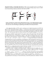
1
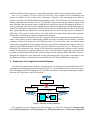
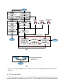
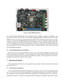
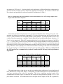
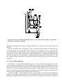
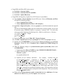
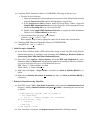
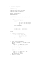
Processor Customization on a Xilinx Multimedia Board
Partha Biswas, Sudarshan Banerjee, and Nikil Dutt,
CECS Technical Report #06-04
Center for Embedded Computer Systems School of Information and Computer Science
University of California, Irvine, CA 92697, USA
Mar 12, 2006
Abstract
Performance of applications can be boosted by executing application-specific Instruction Set Extensions (ISEs) on a specialized hardware coupled with a processor core. Many commercially available
customizable processors have communication overheads in their interface with the specialized hardware.
However, existing ISE generation approaches have not considered customizable processors that have communication overheads at their interface. Furthermore, they have not characterized the energy benefits of
such ISEs. This report presents a soft-processor customization framework that takes an input ‘C’ application and realizes a customized processor capturing the microarchitectural details of its interface with the
specialized unit. The speedup, energy, power and code size benefits of the ISE approach were accurately
evaluated on a real system implementation by applying the design flow to a popular Xilinx Microblaze
soft-processor core synthesized for four real-life applications. It was found that only one large ISE per
application is sufficient to get an average 1.41× speedup over pure software execution in spite of incurring
communication overheads. Finally, a simultaneous savings in energy (up to 40%) and power (up to 12%
peak power reduction) with this increased performance were observed.
1
Contents
1
Introduction
4
2
Customized Processor Model
5
3
Related Work
5
4
Framework for Complete System Realization
4.1 Preprocessing Input Application . . . . .
4.2 ISE Generation Phase . . . . . . . . . . .
4.3 H/W Generation Phase . . . . . . . . . .
4.4 S/W Generation Phase . . . . . . . . . .
4.5 Processor Subsystem Generation Phase .
.
.
.
.
.
.
.
.
.
.
.
.
.
.
.
.
.
.
.
.
.
.
.
.
.
.
.
.
.
.
.
.
.
.
.
.
.
.
.
.
.
.
.
.
.
.
.
.
.
.
.
.
.
.
.
.
.
.
.
.
.
.
.
.
.
.
.
.
.
.
.
.
.
.
.
.
.
.
.
.
.
.
.
.
.
.
.
.
.
.
.
.
.
.
.
.
.
.
.
.
.
.
.
.
.
.
.
.
.
.
.
.
.
.
.
.
.
.
.
.
.
.
.
.
.
.
.
.
.
.
6
7
7
7
8
10
5
Communication Template for Xilinx Microblaze
11
6
Experiments
12
6.1 Experimental Setup . . . . . . . . . . . . . . . . . . . . . . . . . . . . . . . . . . . . . . 12
6.2 System Implementation on the Board . . . . . . . . . . . . . . . . . . . . . . . . . . . . . 13
7
Experimental Results
13
7.1 Performance and Code Size . . . . . . . . . . . . . . . . . . . . . . . . . . . . . . . . . . 13
7.2 Power and Energy Results . . . . . . . . . . . . . . . . . . . . . . . . . . . . . . . . . . 15
7.3 Slices Utilization . . . . . . . . . . . . . . . . . . . . . . . . . . . . . . . . . . . . . . . 16
8
Summary and Future Directions
16
A System Realization on Xilinx Multimedia Board
18
B Steps for System Simulation using ModelSim
21
C Creating a Custom FSL Interface
26
D VHDL Source for the Communication Template
26
E Structural AFU model for adpcm-d
29
F AFU with its Interface for adpcm-d
36
List of Figures
1
2
3
Target Customized Processor Subsystem . . . . . . . . . . . . . . . . . . . . . . . . . .
The Flow of our Framework . . . . . . . . . . . . . . . . . . . . . . . . . . . . . . . . .
(a) A high-level application to a hardware/software system generation (b) Processor subsystem generation . . . . . . . . . . . . . . . . . . . . . . . . . . . . . . . . . . . . . . .
5
6
8
4
5
6
7
8
9
10
The ISE here is composed of the shaded instruction nodes. (a) An example showing the
LastDef point and the FirstUse point; (b1) an example where it is not possible to insert
the ISE under consideration; (b2) After code restructuring; (b3) positioning of the ISE
between LastDef and FirstUse. . . . . . . . . . . . . . . . . . . . . . . . . . . . . . . .
Measuring System Power . . . . . . . . . . . . . . . . . . . . . . . . . . . . . . . . .
A DP-external AFU Interface . . . . . . . . . . . . . . . . . . . . . . . . . . . . . . .
Microblaze Processor Core with an AFU and its Interface. . . . . . . . . . . . . . . . .
Communication Template for AFU Interface in Microblaze . . . . . . . . . . . . . . . .
Xilinx Multimedia Board . . . . . . . . . . . . . . . . . . . . . . . . . . . . . . . . . .
An ISE for ADPCM ENCODER (adpcm-e) having 4 inputs and 2 outputs; each operation
node maps to a hardware component. . . . . . . . . . . . . . . . . . . . . . . . . . . .
.
.
.
.
.
.
9
10
10
11
12
13
. 15
1
Introduction
Typically, applications running on a programmable platform can be executed either as a software algorithm or on a specialized hardware unit. The software approach is the slowest but most flexible while
the hardware approach is the fastest but least flexible. Instruction Set(IS)-extensible processors comprise
an emerging class of processors (especially in the embedded domain) that permit execution of only the
critical application kernels in customized units (as hardware) with the rest of the application executing
on the processor core (as software). This speeds up the application without compromising the processor
clock or modifying the architectural model of the processor and yet preserves the flexibility of the software approach. We call such a coprocessing hardware element an Ad-hoc Functional Unit (AFU). The
AFU operation is triggered by an instruction or a set of instructions that we call an Instruction Set Extension or ISE. In the past, researchers have modeled AFUs having no communication overhead. However,
many commercially popular customizable processors have communication overheads in their interface
with AFUs. Therefore, our goal is to consider the microarchitectural details of an AFU interface in a
processor customization framework and accurately evaluate the performance and energy benefits of ISEs
in a realistic processor. The efficacy of the framework lies in seamlessly considering the synchronization
between the processor and the AFU in a unified manner for different applications.
Minimizing power and energy consumption is as important as maximizing performance in embedded
systems. A high power consumption may destroy a chip completely through overheating while a high
energy consumption may reduce the battery life of an embedded device. Therefore, even though ISEs can
achieve high speedups, designers need to determine if this speedup comes at a price of increased power.
This report shows that increased performance can also reduce both power and energy of a customizable
processor in the presence of an AFU and reports the effects on code size and area.
It is predicted [17] that by 2010, over one-third of all PLD/FPGA devices are expected to have microprocessor cores, up from 15% today. Xilinx Microblaze [10] is a popular commercially-available soft-core.
We demonstrate the use of our framework by transforming a given input application into a running Xilinx Microblaze hardware-software system. For four real-life applications (from Mediabench and EEMBC
suites), we measure the real performance gain over pure software execution and also accurately evaluate
energy and power consumption. Our experimental results show that significant speedup is obtained only
when an ISE contains a large set of atomic operations. With only one large ISE per application, we obtained speedup of up to 1.47× over simple software execution and simultaneously up to 40% energy saving
and 12% peak power reduction. To the best of our knowledge, this is also the first attempt to present the
details of interfacing an AFU with a customizable soft-core. The main contributions highlighted in this
report are the following:
• We present a generalized interface-aware soft-processor customization framework for mapping an
application in C into a running processor-AFU subsystem that enables accurate evaluation of all the
metrics deemed important in embedded system design, namely, performance, energy, power, cost
and code size.
• By applying our framework to Microblaze soft-processor core, we conclude that ISEs can be simultaneously beneficial in terms of performance, energy, power and code size.
The rest of the report is organized as follows. We present our target customizable processor model
in Section 2. In Section 3, we present some related research work. We describe our framework for
transforming a given application to a customized processor subsystem in Section ??. Section 6.1 presents
Processor Subsystem
Program
Memory
Core
DP−external
Register
File
Data
Memory
Bus
External
Tightly−coupled
Execution
Unit
AFU
AFU
External
DP−internal
Interface
Tightly−coupled
Peripherals
Interface
Decoder
AFU
Coprocessor
Loosely−coupled
External
Memory
Figure 1. Target Customized Processor Subsystem
how we use the framework to target Xilinx Microblaze soft-processor core. In Section ??, we describe our
experimental results. Finally, Section 8 concludes the report.
2
Customized Processor Model
Our goal is to map a given application to the target customizable processor model shown in Figure 1.
In this model, the software part of the application stored in the program memory is composed of base instructions to be run on Execution Unit and ISEs to be run on the hardware part, i.e., AFUs. An AFU can be
tightly-coupled with the core through an AFU interface inside the processor subsystem or loosely-coupled
through an external bus. The AFU interface or the external interface implements the communication protocol between the AFU and the processor and thus controls synchronization of data and access to the
processor register file.
The function of an ISE is to transfer control to an AFU for execution. An ISE can be either a single
user-defined instruction or a set of multiple pre-defined instructions. A single user-defined instruction is
decoded as a special instruction, which encapsulates inputs and outputs of an AFU as source and destination operands respectively. The decoder takes the responsibility of issuing such a special instruction to an
appropriate AFU for execution. Alternatively, sending inputs and receiving outputs of the AFU from the
processor can be done at the expense of multiple data transfer instructions. Such instructions must already
exist in the instruction set of the processor in the form of “send data to AFU” and “receive data from
AFU” instructions. In this case, the AFU incurs communication overhead at its interface while sending
and receiving data.
3
Related Work
Several algorithms [1, 4, 2, 3, 5, 6] have recently been proposed to identify ISEs in a given application.
The speedups over simple software execution claimed in most of the approaches [1, 4, 2, 3] are estimated
by assuming a typical RISC processor execution model. The methodology in [5] targets Trimaran research
infrastructure. Using a simulator, the authors show speedup for applications that reuse AFUs generated
for other applications in the same domain. Such reuse of AFUs across application is possible only when
ISEs found were reasonably small in size. However, we will confirm in our experimental results that such
small-sized ISEs would not generate a considerable speedup for AFUs with communication overheads.
Sun et al. [6] employs a Tensilica Instruction Extension (TIE) compiler in their methodology and
operates at a higher (C source-code) level of abstraction. Therefore, this methodology relies more on
designer’s experience for ISE identification and mapping to AFUs. The AFU in this case therefore does not
have any communication overhead. Fei et al. [7] integrated a fairly accurate energy estimation engine in the
same framework, but they do not report a comparison of energy before and after extending the processor. A
recent work having a goal of real system implementation [8] generated application-specific instructions for
Altera Nios II processor in the presence of AFUs that do not have communication overheads. The results
show a good speedup and limited area overhead, but they do not discuss energy or power consumption.
Unlike [8], in this report, we deal with the non-trivial details of synchronization between the processor
and the AFU with the help of a generic communication template.
Note that in the prior related work, the AFU in general did not have communication overheads at its interface. Indeed, there are many commercially available processors providing such an interface. Common
examples are Altera Nios II processor [13], LEON processor [12], etc. However, there are similarly many
commercial customizable processors where AFUs incur overhead in sending and retrieving data. Some examples include STMicroelectronics ST120 [11], Xilinx Microblaze processor [10], etc. To the best of our
knowledge, ISE generation in the context of AFUs incurring communication overheads at their interface
with the core processor has not been studied yet. This is our motivation for proposing a framework that
is capable of incorporating different AFU models and in particular, targeting Xilinx Microblaze soft-core.
We apply the design flow of our framework to study performance gain, energy/power consumption, code
size reduction and area overhead with the introduction of an AFU into the Microblaze subsystem.
4
Framework for Complete System Realization
Our framework takes as input a high-level application (in C), and generates an executable and an AFU
with appropriate interfacing protocol (as shown in Figure 2). The executable runs in the processor core as
software containing ISEs for invoking the AFU operation in hardware. Our target for running the complete
processor-AFU subsystem is an FPGA platform.
Application
ISE Generation
ISEs
Latency
S/W Generation
H/W Generation
Interface
Executable
System
Processor
Core
AFU+Interface
AFU
FPGA
platform
Figure 2. The Flow of our Framework
The expanded view of our framework is shown in Figure 3(a). It has five main phases: Preprocessing
phase, ISE generation phase, S/W generation phase, H/W generation phase, and Processor subsystem
generation phase. The Preprocessing phase takes the input application and generates an annotated intermediate representation. The ISE generation phase generates ISEs under microarchitectural constraints.
The H/W generation phase synthesizes the corresponding AFUs with their interfaces and the S/W generation phase generates the executable. A dotted arrow between the two phases indicates that the latency
of an ISE obtained in the H/W generation phase is passed on to the S/W generation phase. Finally, the
Processor subsystem generation phase builds the complete running system for evaluation.
4.1
Preprocessing Input Application
This phase can be identified as a box labeled “Preprocessing” in Figure 3(a). A compiler front-end
yields Control Flow Graph (CFG) and Data Flow Graph(DFG) of an input application and runs predication to combine a set of small basic blocks into a large basic block. The input application is then profiled
and the basic blocks are annotated with their execution counts. A component library is created containing a synthesizable combinational element corresponding to each instruction in the target instruction set.
Each element in the library is synthesized for a given technology and the corresponding instruction in the
DFG is annotated with a normalized hardware latency. Each instruction in the DFG is also annotated with
its software latency obtained from the target architecture specification.
4.2
ISE Generation Phase
This phase (shown as the “ISE generation” box in Figure 3(a)) is integrated with the compiler frontend. An ISE generation algorithm takes the annotated CFG/DFG and returns subgraphs or ISEs that would
maximize performance under microarchitectural constraints. Although any ISE generation algorithm can
be used, we use ISEGEN in our framework because it identifies all the instances of an ISE exploiting
large-scale ISE reuse.
4.3
H/W Generation Phase
We show this phase in a box marked “H/W generation” in Figure 3(a). The two subtasks of this
phase are component library binding and interface synthesis. The identified subgraph or ISE is isolated
and each instruction in the subgraph is replaced by the corresponding element in the component library.
Figure 10 shows an example subgraph where each node maps to an element in the component library. The
data dependencies between the instructions are replaced by port-to-port connections between the elements
and the resulting structure is an AFU. This structural AFU model is then synthesized to evaluate the critical
path length. The critical path length divided by the clock period of the processor core gives the number of
cycles needed for the AFU operation. This latency information is passed on to the scheduler in the S/W
generation phase (shown with a dotted arrow in Figure 3). The evaluated number of cycles is also used to
synchronize the AFU with respect to the core.
Apart from the component library, the designer also creates a communication template for AFUs,
which captures the communication protocol between the processor core and the AFU. The writing back
of result from the AFU to the processor is delayed by the exact number of cycles required by the AFU
operation. The implementation of communication protocol together with synchronization with the core
completes the AFU interface synthesis. Note that the H/W generation phase can be applied to synthesize
the AFU and its interface in the customized processor model presented in Figure 1.
Application
Preprocessing
Compiler
Front-end
Profile code
CFG/DFG
Annotate w/ hw/sw
latencies, exec count
S/W generation
ISE generation
Replace
subgraph by ISE
Component
Library
Constraints
Communication
Template
Annotated
CFG/DFG
CFG/DFG
w/ ISEs
ISEGEN
Scheduling
Register Alloc
ISEs or
subgraphs
Compiler
Back-end
H/W generation
Component Library Binding
Replace ops by
components and
edges by cnxns
Executable
Clock
Period
Interface Synthesis
Structural
AFU model
Eval Crit. Path
Calc # Cycles
Couple
Computation w/
Communication
AFU +
Interface
# Cycles
Latency
(a)
AFU +
Interface
Processor
model
Synthesis
P/R
Processor Subsystem
generation
System
(b)
Figure 3. (a) A high-level application to a hardware/software system generation (b) Processor subsystem
generation
4.4
S/W Generation Phase
This phase (shown in Figure 3(a) as a box titled “S/W generation”) generates code for the target
processor taking into account the presence of AFUs. The two subtasks in the S/W generation phase are
subgraph matching and subgraph replacement with ISEs. Since all possible instances of an ISE have
already been enumerated by the ISE generation phase, the subgraph matching simply consists of a DFG
traversal and marking constituent instructions of the ISE in the DFG.
1
LastDef
2
3
FirstUse
1
1
3
2
FirstUse
3
LastDef
1
3
LastDef
2
FirstUse
4
4
4
4
2
5
5
5
5
(a)
(b1)
(b2)
(b3)
Figure 4. The ISE here is composed of the shaded instruction nodes. (a) An example showing the LastDef
point and the FirstUse point; (b1) an example where it is not possible to insert the ISE under consideration; (b2) After code restructuring; (b3) positioning of the ISE between LastDef and FirstUse.
After subgraph matching, the ISE is used to replace the set of marked instructions in the DFG. We
depict the ISE replacement strategy in Figure 4. An ISE can be placed anywhere between the point
where its source operands have their last definition (LastDef) and the point where its destination operand
has its first use (FirstUse) as shown in Figure 4(a) (the shaded nodes identify the ISE under consideration). Since ISE generation phase has ensured convexity of the identified subgraphs, it is never possible to have a dependency edge from the FirstUse node to the LastDef node because this would make
the subgraph non-convex. Consequently, it is possible to encounter a situation where a FirstUse point
precedes a LastDef point in the instruction sequence. This renders the subgraph replacement impossible without code restructuring. Consider the following sequence of operations in instruction order:
(1)a = b ∗ c; (2)f = a|0x2; (3)e = 5; (4)d = a + e; (5)g = e − d. Suppose the ISE under consideration is
a multiply followed by an add, as identified by the nodes labeled 1 and 4 in Figure 4(b1) respectively. Figure 4(b1-b3) show an example of how the placement of ISE between LastDef and FirstUse is accomplished
through code restructuring. Since in this case the FirstUse point appears earlier in the instruction chain
than the LastDef point, the ISE cannot be placed anywhere (Figure 4(b1)). So, instruction reordering has
to be done in order that the LastDef point precedes the FirstUse point. This reordering is possible because
there is no dependency from FirstUse to LastDef. Figure 4(b2) shows the code snippet after restructuring
Figure 4(b1) (i.e., swapping the positions of node 2 and node 3) and Figure 4(b3) shows the placement of
ISE between the LastDef point (node 3) and the FirstUse point (node 2).
If an ISE is used as a single user-defined instruction, a single instruction just replaces the set of
constituent instructions. Replacing the multiply and the add with a single user-defined instruction
(ISE1(·, ·, ·)), the resulting instruction sequence (as in Figure 4(b3)) would become: (3) e = 5; (1),(4)
d = ISE1(b, c, e); (2) f = a|0x2; (5) g = e − d. However, if an ISE is represented as a set of predefined
data transfer instructions (send(·), receive(·)), the resulting instruction sequence after ISE replacement
would appear as: (3) e = 5; (1),(4) send(b); send(c); send(e); receive(d); (2) f = a|0x2; (5) g = e − d.
After subgraph replacement with ISE, the compiler performs scheduling, register allocation and target
code generation as a back-end pass. Note that the latency of the ISE required by the scheduler is derived
Executable
Memory
Image
System
Superimpose
Structural
Model
Timing
Info
Hardware
Simulation
Routing
Info
Power
Simulation
VCD
Power
Report
Figure 5. Measuring System Power
from the H/W generation phase as shown in Figure 3(a).
4.5
Processor Subsystem Generation Phase
We show this phase in Figure 3(b). As a final step, the processor model of the target Soft-core along
with the AFU and its interface are synthesized and implemented using standard synthesis and Placeand-Route tools. The executable generated in Figure 3(a) and the system synthesized in Figure 3(b) are
deployed in two schemes, one for measuring speedup and the other for evaluating energy/power consumption. With the goal of measuring actual time spent in running the application, the scheme for Performance
Measurement uses the bitmap of the synthesized system to program an FPGA fabric, which then becomes
the platform for actually running the executable. The executable is downloaded into the system memory
through a JTAG port and the number of cycles for running the executable is measured using a hardware
timer.
Program
Memory
Processor
Subsystem
Core
Tightly−coupled
Register
File
Data
Memory
Bus
Interface
Execution
Unit
External
AFU
External
DP−external
AFU
Interface
Decoder
Peripherals
External
Memory
Figure 6. A DP-external AFU Interface
Since there is no direct way to measure power of a running system on the FPGA fabric, we employ
a different scheme for Power/Energy Evaluation (depicted in Figure 5) for accurately evaluating the
power and energy consumption of the system. Note that there are three kinds of information in the post-
Place-and-Route system (Figure 3(b)): the structural model of the system, the timing information and
the routing information. We superimpose the memory image of the executable (in Figure 3(a)) into the
memory section of the structural model. This complete structural model along with the timing information
is run through a cycle-accurate hardware simulator to generate a Value Change Dump (VCD) of all the
signals in the structural netlist. The routing information and the VCD information together are then used
by a power simulator to generate the dynamic power consumed at different time steps. We then derive the
total energy dissipated in the system from the reported power and the measured execution time.
Now, we apply our processor customization framework to generate a real system.
5
Communication Template for Xilinx Microblaze
Xilinx Microblaze [10] is a soft-core with a DP-external AFU interface (as shown in Figure 6). We
demonstrate the utility of our framework by transforming a given input application into a running Microblaze hardware-software system.
Microblaze has a DP-external AFU to be connected with the processor via Fast Simplex Links (or
FSLs). FSLs are dedicated point-to-point unidirectional 32-bit wide FIFO interfaces. The Microblaze is
capable of including a maximum of 8 input and 8 output FSLs.
Counter
Count
Microblaze
Processor
FSL
8X8
Cnt_en
AFU
Int.
AFU_en
In
AFU
Out
CLK
Figure 7. Microblaze Processor Core with an AFU and its Interface.
Microblaze is a 32-bit RISC processor with a simple 3-stage pipeline. Figure 7 shows an AFU and its
interfacing with the Microblaze processor core via 8 × 8 FSL channels. The AFU interface implements
the processor-AFU communication protocol and is synchronous with the Microblaze processor through a
global clock (CLK). The AFU interface is also connected to a counter module to enable counting whenever
required. If the count enable signal (Cnt en) is ‘1’, counting is enabled. Otherwise, the counter is reset to
‘0’. The signals In[32] and Out[32] are used to send data to and receive data from the AFU respectively.
When the AFU-enable signal, AFU en is ‘1’, the AFU latches the output in Out[32].
In Figure 8, we present the generic communication template for Microblaze-AFU interaction as a
Finite State Machine (FSM) synchronous with respect to CLK. For the sake of explanation, we call an
FSL channel FSL R when it is used for AFU read operation or FSL W when it is used for AFU write
operation. Associated with every FSL R channel is a set of three signals, namely, (FSL READ SIG,
FSL DATA EXISTS, FSL IN DATA[32]).
Another triplet, (FSL WRITE SIG, FSL FIFO FULL,
FSL OUT DATA[32]) is associated with every FSL W channel. The FSM is initially in “Input Sync” state
waiting for data to arrive on an FSL R channel. When data exists on the FSL channel, the corresponding
FSL DATA EXISTS signal goes high causing a transition from “Input Sync” state to “Input Read” state.
In “Input Read” state, FSL READ SIG is set to high to cause the data in the FSL R FIFO to be read into
(FSL_DATA_EXISTS == ‘low’)
(FSL_DATA_EXISTS == ‘high’)
Input−Sync
Input−Read
FSL_READ_SIG <= ‘0’
FSL_READ_SIG <= ‘1’
FSL_WRITE_SIG <= ‘0’
Cnt_en <= ‘0’
In <= FSL_IN_DATA
AFU_en <= ‘0’
true
true
FSL_OUT_DATA <= Out
FSL_WRITE_SIG <= ‘1’
FSL_READ_SIG <= ‘0’
AFU_en <= ‘1’
AFU_en <= ‘0’
Cnt_en <= ‘1’
Output−Write
Output−Sync
(Count == # Cycles) and
(FSL_Q_FULL == ‘low’)
(Count != # Cycles) or
(FSL_Q_FULL == ‘high’)
Figure 8. Communication Template for AFU Interface in Microblaze
In[32] using a 32-bit signal array, FSL IN DATA. After the data has been read into In[32], the FSM transitions to “Output Sync” state and waits on the AFU operation by enabling the counter. After # Cycles
(as evaluated in the H/W generation phase in Figure 3(a)) has elapsed, the result of the AFU operation is
latched in Out[32]. If FSL W FIFO is not full (i.e., FSL FIFO FULL is low), a state transition takes place
to “Output Write” state. In the “Output Write” state, data from Out[32] is written into the FSL W FIFO
using FSL OUT DATA[32] by setting FSL WRITE SIG to high. Thus, for introducing every new AFU,
only the AFU module in Figure 7 and the # Cycles change in the process of H/W generation, while the
communication template is reused.
6
Experiments
We first describe our experiemental setup in detail and then present the experimental results.
6.1
Experimental Setup
The ISE generation algorithm (ISEGEN) [1] was integrated with a MACHSUIF [9] front-end. The
S/W generation was done with Microblaze GCC-2.95 (mb-gcc) compiler. Microblaze Instruction Set has
multiple data-transfer instructions for sending data to and receiving data from its FSL channels — put for
sending and get for receiving data in blocking mode, and nput/nget are the corresponding instructions in
non-blocking mode. We used the non-blocking send instruction (nput) and the blocking receive instruction (get) for our AFU interface. Because of using two different compilers for ISE generation and S/W
generation, the subgraph replacement with ISEs was done as a post-assembly pass on the assembly output of mb-gcc. After replacing the identified subgraphs with ISEs, mb-gcc was run again to generate the
executable.
We selected four real-life applications for demonstrating the effectiveness of our framework: autcor
(Auto-correlation) from EEMBC suite, adpcm-e (ADPCM Encoder) and adpcm-d (ADPCM Decoder)
from Mediabench suite, and AES (AES encryption). Our platform is Xilinx Multimedia Board, which is
equipped with a Virtex-II XC2V2000 FPGA. Figure 9 shows a snapshot of the board. We used Xilinx Platform Studio for configuring the FPGA to include a Microblaze processor with a 64KB (i.e., the maximum
Figure 9. Xilinx Multimedia Board
size possible) Block RAM (BRAM), two Local Memory Buses (LMBs) (to interface with BRAM – one
for instruction and the other for data), one Microblaze Debugging Manager (MDM) and one Timer (both
MDM and Timer on a single On-chip Peripheral Bus (OPB)). The standard inputs and outputs of an application were redirected to the MDM and the elapsed number of cycles was evaluated using the Timer. We
set the clock frequency of the Microblaze processor to 50 MHz. The tools used in the second scheme (Figure 5) for evaluating energy and power are ModelSim for hardware simulation [15] and Xilinx XPower for
power simulation [16]. We now detail the steps to realize a complete hardware-software subsystem using
the Xilinx Multimedia Board.
6.2
System Implementation on the Board
The steps that we used to build a Hardware-Software system using Xilinx Embedded Development Kit
(EDK) are enumerated in Appendix A. The generated system can be simulated both behaviorally as well
as structurally following the steps detailed in Appendix B. Appendix C briefly explains how an AFU is
introduced in the form of a user core in the system.
7
Experimental Results
We demonstrate the effectiveness of our approach using a number of front-end tools in our framework
shown in Figure 3(a).
7.1
Performance and Code Size
The code generation for the baseline configuration was done by mb-gcc with all optimizations turned
on (-O2, -mnoxl-soft-mul) so that the performance is maximized in pure software execution. The Microblaze configuration was then customized for different applications by introducing AFU with its interface as
explained in Section 6.1. The ISEs were generated with I/O constraints of maximum 4 inputs and 2 outputs
and number of AFUs set to 1. Note here that for each application, a different Microblaze configuration is
generated and the resulting system is analyzed by applying our framework. The results in terms of code
size reduction and speedup over software execution are summarized in Table 1.
Table 1. Speedup and Code Size Reduction with the Introduction of an AFU having 4 inputs and 2
outputs in the Microblaze subsystem
BMs
autcor
adpcm-d
adpcm-e
AES
Core Only
Bytes Cycles
58444 264305
12049 252688
14121 157177
16013 240613
Core + AFU
Bytes Cycles
58452 404673
11953 190979
13989 106821
14957 167397
Code
Redn
-8
96
132
1056
Spdup
0.65×
1.32×
1.47×
1.44×
Each of the operand-send and result-receive operations in Microblaze has a latency of 2 cycles. Consequently, the latency for transferring 6 operands is 12 cycles in the worst case and 6 cycles in the best
case (i.e., if all the latencies are successfully hidden by the scheduler). The ISE generated for autcor was
a chain of just three operations: a multiply, a barrel right shift and an add having software latencies as 3,
2 and 1 cycles respectively. With AFU operation taking just 1 cycle, the best case latency of the ISE is
6 + 1 = 7 cycles. Thus, even the best case performance of the ISE lags behind the worst case performance
of the corresponding software execution (3+2+1 = 6 cycles). Consequently, there was slowdown instead
of speedup for autcor owing to the communication overhead. However, there are some prior related work
[6, 8], which have shown speedup even with small-sized ISEs containing on the order of 3-4 instructions
because of incurring no communication overhead in processor-AFU interface. Thus, we confirm that if
the AFU interface has a communication overhead, a small-sized ISE will only result in performance
degradation.
Table 2. Power Benefits of ISEs in the Microblaze subsystem
BMs
autcor
adpcm-d
adpcm-e
AES
Core Only
P. Pwr A. Pwr
(mW) (mW)
1957
1287
1975
1317
2070
1332
2256
1276
Core + AFU
P. Pwr A. Pwr
(mW) (mW)
1869
1229
1919
1197
2012
1178
1982
1187
% Pk
Pwr
Redn
4.5
2.8
2.8
12.1
% Avg
Pwr
Redn
4.5
9.1
11.6
7.0
The applications adpcm-d and adpcm-e are the two examples where predication of several small critical
basic blocks led to a large basic block. Consequently, the ISEs found for these two benchmarks are
very large containing on the order of 40 operations. This led to a significant speedup in spite of the
communication overhead. Figure 10 shows the ISE of adpcm-e that generated a speedup of 1.47× over
pure software execution. The shaded nodes show the inputs and the outputs of the ISE. Appendix D,
in2
in1
’0’
==
’0’
’8’
1
0
sel
−
>=
==
−
in4
in3
0 1
sel
in3
’4’
>>
−
<
1 0
sel
’3’
1
0
sel
1 0
sel
’1’
+
>>
’2’
−
or
1 0
sel
1 0
sel
or
1 0
sel
or
out1
1
sel
in2
0
>>
+
<
1 0
sel
−
in2
+
0
’32767’
’−32768’
’1’
+
’1’
’4’
*
<
1
sel
0 1
sel
0
1
’32767’
<=
’−32768’
>=
sel
out2
Figure 10. An ISE for ADPCM ENCODER (adpcm-e) having 4 inputs and 2 outputs; each operation
node maps to a hardware component.
Appendix E and Appendix F present the complete VHDL source code for the AFU and its interface for
adpcm-d.
The last benchmark under consideration is AES, which has the largest number of instructions in its
critical basic block. The generated ISE [1] had 8 instances in the critical basic block covering more than
50% of the DFG and overall 12 instances in the critical function. Both the large size and large-scale reuse
(as defined in [1]) of the ISE accounts for a significant speedup (1.44×) obtained on AES despite the
overhead in sending and receiving operands. Along with the merit of speedup, AES also exhibit a 7% code
size reduction owing to replacement of a large chunk of code by an ISE in the form of a set of data transfer
instructions.
7.2
Power and Energy Results
From Table 2, it is evident that both the peak power (P. Pwr) as well as the average power (A. Pwr)
reduced with the introduction of AFU. Because the presence of both core and AFU apparently indicates
more circuit activity, an initial expectation is increased power with the addition of AFU. However, because
the ISE here is a multi-cycle operation interlocked with the Microblaze pipeline, the AFU operation completely overlaps with a processor pipeline stall. Consequently, we obtain an overall power reduction in the
presence of AFU operation owing to reduced overall circuit activity.
As shown in Table 3, we also obtained up to 40% saving in energy on account of reduced application
runtime. It is interesting to note that the trend of energy decrease (or increase) exactly follows that of
speedup (shown again in Table 3 for the sake of comparison). This trend can be expected as a corollary to
Table 3. Energy Benefits of ISEs in the Microblaze subsystem
BMs
autcor
adpcm-d
adpcm-e
AES
Tot Energy (µJ)
for Core Only
2.21
8.48
10.54
69.09
Tot Energy (µJ)
for Core+AFU
3.10
5.84
6.34
43.69
%age
Saving
-40.27
31.13
39.85
36.76
Spdup
0.65×
1.32×
1.47×
1.44×
a consistent power reduction shown in Table 2. Thus, contrary to conventional expectation, enhanced
performance simultaneously results in reduced power and energy for the customized Microblaze
soft-core.
7.3
Slices Utilization
The XC2V2000 FPGA that we use as our target platform has 10752 slices. Table 4 shows the percentage utilization of the FPGA slices before and after introducing the AFU that brought the speedup in
Table 1.
Table 4. Slices Utilization (out of 10752) in the absence of an AFU and in the presence of an AFU for the
four applications in XC2V2000 FPGA
BMs
Slices
Util.
No AFU
1274
11%
autcor
1609
14%
adpcm-d
1804
16%
adpcm-e
2226
20%
AES
2043
19%
Note here that XC2V2000 used here is very small. The largest possible Virtex-II chip, XC2V8000
contains 46592 slices. If the largest FPGA is used instead of XC2V2000, the average slices utilization
reduces to only 5%, which is very reasonable. Thus, the area overhead of including an AFU in the
Microblaze subsystem is also minimal.
8
Summary and Future Directions
Applications can be accelerated in a programmable processor by executing their performance-critical
sections in customized Ad-hoc Functional Units (AFUs) as Instruction Set Extensions (ISEs). We presented an interface-aware processor customization framework that enabled us to implement a customizable
soft-core microarchitecture capturing the details of interfacing with an AFU. We applied our framework
to four real-life applications and realized four different processor configurations. Our results confirmed
that in the presence of communication overhead at the processor-AFU interface, significant speedup over
pure software execution is possible only if the AFU function is sufficiently larger than a set of 2-3 operations. Further analysis of the synthesized systems led to the conclusion that integration of AFUs in a
customizable processor can result in increased performance and reduced code size, while simultaneously
decreasing power and energy consumption. Our future work will investigate the advantages of ISEs in
other reconfigurable platforms and commercially available processors.
References
[1] P. Biswas, S. Banerjee, N. Dutt, L. Pozzi and P. Ienne. ISEGEN: Generation of High-Quality Instruction Set Extensions by Iterative Improvement. In Proc. of DATE, 2005.
[2] P. Biswas, V. Choudhary, K. Atasu, L. Pozzi, P. Ienne and N. Dutt. Introduction of Local Memory
Elements in Instruction Set Extensions. In Proc. of DAC, 2004.
[3] K. Atasu, L. Pozzi and P. Ienne. Automatic Application-Specific Instruction-Set Extensions under
Microarchitectural Constraints. In Proc. of DAC, 2003.
[4] P. Yu and T. Mitra. Scalable Custom Instructions Identification for Instruction-Set Extensible Processors. In Proc. of CASES, 2004.
[5] N. Clark, H. Zhong and S. Mahlke. Processor Acceleration through Automated Instruction Set
Customization. In Proc. of MICRO, 2003.
[6] F. Sun, S. Ravi, A. Raghunathan and N. K. Jha. Synthesis of Custom Processors based on Extensible
Platforms. In Proc. of ICCAD, 2002.
[7] F. Sun, S. Ravi, A. Raghunathan and N. K. Jha. A Hybrid Energy-Estimation Technique for Extensible Processors. IEEE TCAD, 2004.
[8] J. Cong, Y. Fan, G. Han and Z. Zhang. Application-Specific Instruction Generation for Configurable
Processor Architectures. In Proc. of FPGA, 2004.
[9] Machine SUIF. http://www.eecs.harvard.edu/hube/software/software.html.
[10] Microblaze Processor Reference Guide. http://www.xilinx.com/ise/embedded/mb_
ref_guide.pdf.
[11] ST100 DSP Core Architecture Overview. http://www.st.com/stonline/prodpres/
dedicate/st100/overview/overview.htm.
[12] The Leon Processor User Manual. http://www.ra.informatik.uni-stuttgart.de/
˜virazela/LP_Project/leon-2.3.7.pdf.
[13] The Nios II Processor Reference Handbook. http://www.altera.com/literature/hb/
nios2/n2cpu_nii5v1.pdf
[14] SC140 DSP Core Reference Manual. http://www.soc.napier.ac.uk/module.php3?
op=getresource&cloaking=no&resourceid=1473119.
[15] ModelSim SE datasheet http://www.model.com/products/pdf/datasheets/se.
pdf
[16] Xilinx XPower Documentation http://toolbox.xilinx.com/docsan/xilinx6/
books/data/docs/dev/dev0089_14.html
[17] Panelists peer into future of FPGAs. Article 60407325, EETimes. March 7, 2005.
A
System Realization on Xilinx Multimedia Board
Here we present the detailed steps to realize a basic hardware-software subsystem with the hardware
consisting of the Microblaze processor, local memory bus, BRAM, timer and mdm and the software being
the Microblaze executable.
1. Invoke Xilinx Platform Studio (XPS) 6.2i (or higher).
2. Click File→New Project→Platform Studio. The settings for Create New Project are as follows:
Project File: <Path to work directory>/system.xmp
Target Device Architecture:
virtex2
Device Size:
xc2v2000
Package:
ff896
Speed Grade:
-6 (default)
3. Click OK and then answer Yes for Do you want to start with an empty MHS File? Then click OK
for the comment Project→Add/Edit Cores.
4. Setting up the hardware: Under System tab, right click on System BSP and select Add/Edit
Cores ....
(a) Add the following peripherals:
• microblaze (1)
• bram block (1)
• lmb bram if cntlr (2) (1 for data; 1 for instruction): Base Address = 0x00000000; High
Address = 0x0000ffff (Memory allocated both for data and instruction = 64 KB)
• opb mdm (1): Base Address = 0xffff0400; High Address = 0xffff04ff
• opb timer (1): Base Address = 0xffff0800; High Address = 0xffff08ff (Note that address
ranges chosen are disjoint)
(b) Add the following bus connections:
• lmb v10 v1 00 a (2):
microblaze 0 dlmb (M), lmb bram if cntlr 0 slmb (S),
microblaze 0 ilmb (M), lmb bram if cntlr 1 slmb (S)
• opb v20 v1 10 b (1):
microblaze 0 dopb (M), microblaze 0 iopb (M),
opb mdm 0 sopb (S), opb timer 0 sopb (S)
(c) All the Clk and Rst ports. All the net names must be sys clk or sys rst corresponding to Clk
and Rst ports respectively.
(d) The following parameters need to be changed from their default values:
• microblaze 0:
C DEBUG ENABLED = 1,
C USE BARREL = 1 (to use a barrel shifter),
C NUMBER OF RD ADDR BRK = 1,
C NUMBER OF WR ADDR BRK = 1
• opb mdm 0: C UART WIDTH = 8
• lmb v10 0: C EXT RESET HIGH = 0
• lmb v10 1: C EXT RESET HIGH = 0
• opb v20 0: C EXT RESET HIGH = 0
Click OK to register all the above changes for the hardware.
5. Setting up the software: In the Applications tab, right click on Software Projects and click Add
New Project. Give a name to the project and click OK.
(a) Right click on Sources and click Add File... Select all the source (*.c) files and click OK.
(b) Right click on Headers and click Add File... Select all the header (*.h) files and click OK.
(c) Right click on Default: microblaze 0 xmdstub and click to Mark to Initialize BRAM.
(d) Right click on Project: <Project name> and click to un-select Mark to Initialize BRAM.
(e) Right click on Project: <Project name> and select Set Compiler Options. Under Directories tab, give a suitable path for Output ELF File, for example, <Path to work
directory>/output/executable.elf. (If barrel shifter is present in the Microblaze, i.e., if
C USE BARREL = 1, then, under the Advanced tab, insert -mxl-barrel-shift in the Program
Sources Compiler Options.)
6. Select Project→Software Platform Settings.
(a) In the Processor and Driver Parameters tab, change the Current Value of xmdstub peripheral
to opb mdm 0.
(b) In the Library/OS Parameters tab, change the Current Values of both stdin and stdout to
opb mdm 0.
7. Create a User Constraints File in <path to work directory>/data/system.ucf with the following
lines (for Xilinx Multimedia Board):
NET ”sys clk” LOC = ”AD16”;
NET ”sys rst” LOC = ”AH7”;
NET ”sys clk” NODELAY;
NET ”sys clk” TNM NET=”clk50”;
TIMESPEC ”TSclk50”=PERIOD ”clk50” 20 ns HIGH 50%;
Note that the pin mapping will alter if the board is different. The clock frequency is selected to be
50 MHz with 50% duty cycle.
8. Synthesizing the hardware (to be carried out by one the following ways):
• Using EDK with Xilinx XST (easier option):
(a) Run Tools→Generate Netlist.
(b) Run Tools→Generate Libraries and BSPs.
(c) Run Tools→Update Bitstream.
• Using EDK with Synplicity Synplify Pro (if XST license is unavailable):
(a) Open Options→Project Options from the XPS menu. Select tab Hierarchy and Flow
and make the following changes:
i. Change Synthesis Tool to None.
ii. Change Implementation Tool Flow to ISE (ProjNav).
(b) Run Tools→Export to ProjNav. A directory projnav is created that contains the exported
files.
Note that if Xilinx Platform Studio has been installed after XST has expired, an error will
be reported saying “[ERROR] Unable to set property: Synthesis Tool”. To resolve this
error, run a script containing the following in the <Path to work directory>/ directory.
sed ’/XST/d’ npl cmdfile > tmpfile
mv tmpfile npl cmdfile
pjcli -v -f npl cmdfile
(c) Invoke (from Windows menu) Xilinx ISE→Project Navigator.
(d) Click File→Open Project and open system.npl to be found in the projnav directory.
(e) Double-click xc2v2000-6ff896 (to be found under Sources in Project) to open Project
Properties. Change the value of Synthesis Tool to Synplify Pro (VHDL/Verilog) and
click OK.
(f) Make the following changes in system-structure(<path>/system.vhd) (found under
xc2v2000-6ff896):
i. Comment the lines library UNISIM; and use UNISIM.VCOMPONENTS.ALL;
ii. Add the following lines in the beginning:
LIBRARY synplify;
use synplify.attributes.all;
iii. Comment all the attribute statements.
For example, “–attribute box type
of bram block 0 wrapper: component is ”black box”;” for the component
“bram block 0 wrapper”. Instead, introduce for each component, the following
lines: “attribute syn black box of <component name>: component is true;” and “attribute syn noprune of <component name>: component is true;”. The attribute statements were pertaining to XST and Synplify Pro would simply ignore them. So, the
“black box” constraints are specified in Synplicity syntax. If the system does not have
any output, the Synthesis phase would prune all the components. This is prevented by
using syn noprune attribute.
(g) Right-click on system-structure(<path>/system.vhd) and select Add Source. Find system.ucf in the data directory and click Open to add constraints.
(h) Select system-structure(<path>/system.vhd). Double-click Synthesize—Synplify Pro
in Processes for Source section to run synthesis. (Alternatively, double-click Generate
Programming File directly which includes running synthesis and Place-and-Route.)
(i) Double-click Implement Design to perform Place-and-Route of the design.
(j) Double-click Generate Programming File to generate the bitmap file.
(k) Go back to XPS. Select Tools→Import from ProjNav and import the following files:
i. BIT file: <path to work directory>/projnav/system.bit and
ii. BMM file: <path to work directory>/implementation/system bd.bmm.
(l) From the XPS menu, run Tools→Update Bitstream.
9. Compiling the software: Run Tools→Build All User Applications. Check whether the size of
executable.elf is less than 64 KB. (Recall that the memory allocated for both data and instruction
was 64 KB) Also note that the maximum usable space in 56 BRAMs is 64 KB. If not, it is not
possible to run with only BRAMs. The alternatives are out of the scope of this document.
10. Running the system:
(a) Switch on the board and invoke iMPACT from Xilinx ISE→Accessories.
(b) Configure devices via Boundary-Scan Mode with Automatically connect to cable and identify Boundary-Scan chain selected. Select appropriate device to program (e.g., xc2v2000 in
our case).
(c) Right-click on the device and select Assign New Configuration File. Find download.bit in
<path to work directory>/implementation/ directory and select Open. (Observe the PROG
LED change color from red to green indicating success.) Close the iMPACT window.
(d) Create a file xmd.ini in <path to work directory>/ with the following lines:
help
mbconnect mdm
dow mblaze/code/executable.elf
rst
con
(e) From the XPS menu, run Tools→XMD and check the output of running executable.elf (software) on the synthesized hardware.
B
Steps for System Simulation using ModelSim
A complete system simulation is intended for verifying the correctness and generating the Value
Change Dump (VCD) for the different signals employed. The correctness is ensured using both the behavioral simulation as well as the structural (Post-Place-and-Route) simulation. The VCD is relevant only
after the flattened netlist has been generated. After the VCD dump is generated by the structural simulation
run, XPower is employed to evaluate the system in terms of power and energy consumption.
The steps required for taking the design from the EDK into the Project Navigator and running the
behavioral and structural simulation are as follows:
1. Creating Simulation libraries
(a) Compiling Xilinx Simulation Libraries (COMPXLIB): Following are the two ways.
• From the Project Navigator:
i. Open an existing project (that might have been exported from Xilinx Platform Studio
using the Export to ProjNav option) and highlight the target device.
ii. In the Processes for Source window, under the Design Entry Utilities, right-click
Compile HDL Simulation Libraries and select Properties. Select appropriate Target
Simulator (ModelSim SE in our case) and click OK.
iii. Double-click Compile HDL Simulation Libraries to compile the Xilinx Simulation
Libraries (in C:/Xilinx/vhdl/mti se directory).
• From Command Line (shown for virtex2 board):
compxlib -s mti se -f virtex2 -l vhdl
Run compxlib -help to choose appropriate option for the board under consideration.
(b) Compiling EDK Behavioral Simulation Libraries (COMPEDKLIB):
Compedklib.bat -s mti se -o edklib -X
2. Initial Set-up for Simulation
(a) Invoke Xilinx Platform Studio (XPS) and load the design created with XPS (using ProjNav
implementation flow) as explained in the document titled Building a Hardware-Software
system using Xilinx EDK and Xilinx Multimedia Board.
(b) From XPS, select Options→Project Options, and in the HDL and Simulation tab, select
Simulation Model as Behavioral. Set appropriate paths for the simulation libraries as follows:
(Check the installation directories of the ModelSim libraries)
EDK Library: C:/Xilinx/vhdl/mti se/edklib
Xilinx Library: C:/Xilinx/vhdl/mti se
(c) Right click on Project: <Project name> and make sure Mark to Initialize BRAM is selected.
(d) Right click on Default: microblaze 0 xmdstub and make sure Mark to initialize BRAM is
un-selected.
3. Behavioral Simulation using ModelSim
(a) From XPS, invoke Tools→Sim Model Generation (which populates simulation/behavioral
directory). Modify simulation/behavioral/system init.vhd by commenting the last few lines
as follows:
--configuration system\_conf of system is
-- for STRUCTURE
-- for all : bram1\_wrapper use configuration work.bram1\_conf;
-- end for;
--end for;
--end system\_conf;
(b) Now, from Project Navigator, add projnav/testcase.vhd with the following content:
-- TestBench Template
LIBRARY ieee;
USE ieee.std_logic_1164.ALL;
USE ieee.numeric_std.ALL;
ENTITY testbench IS
END testbench;
ARCHITECTURE behavior OF testbench IS
-- Component Declaration
COMPONENT system
PORT(
sys_clk : IN std_logic;
sys_rst : IN std_logic
);
END COMPONENT;
SIGNAL clk :
SIGNAL rst :
std_logic;
std_logic;
BEGIN
-- Component Instantiation
uut: system PORT MAP(
sys_clk => clk,
sys_rst => rst
);
--
Test Bench Statements
tb_clk : PROCESS -- 50 MHz clock
BEGIN
clk <= ’1’; wait for 10 ns;
clk <= ’0’; wait for 10 ns;
END PROCESS tb_clk;
tb_reset : PROCESS
BEGIN
rst <= ’0’; wait for 1 us;
rst <= ’1’; wait;
END PROCESS tb_reset;
-- End Test Bench
END;
-- Check the system_init.vhd file for ensuring the correctness of the module names
configuration testbench_conf of testbench is
for behavior
for uut: system
for STRUCTURE
for all : bram_block_0_wrapper use configuration work.bram_block_0_conf; end for;
end for;
end for;
end for;
end testbench_conf;
(c) Create a script file, projnav/projnav.do with the following content: (a script for behavioral
simulation)
cd ../simulation/behavioral
do system.do
vcom -93 -work work system.vhd
vcom -93 -work work ../../projnav/testbench.vhd
vsim -Lf unisim -t ps +notimingchecks work.testbench conf
add wave *
(d) Right-click on system-structure(<path>/system.vhd) and select Add Source. Find testbench.vhd in the projnav directory and click Open to add test bench. Select vhdl testbench
while adding the test bench.
(e) Click on testbench-behavior (testbench.vhd). Right-click on Simulate Behavioral Model
in the Processes for Source partition and select properties. Change the following fields:
• Use Custom Do File: Check the selection.
• Use Automatic Do File: Uncheck the selection.
• Custom Do File: Click and browse for projnav/projnav.do.
(f) Double-click ”Simulate Behavioral Model” to run the behavioral simulation.
4. Structural/Timing Simulation using ModelSim
(a) Right click on Project: <Project name> and click to Mark to Initialize BRAM.
(b) Right click on Default: microblaze 0 xmdstub and click to un-select Mark to initialize
BRAM.
(c) Invoke Tools→Sim Model Generation: This populates the simulation/structural directory.
(d) The file system init.vhd contains the memory map of the executable. A part of it looks like
the following:
configuration bram1 conf of bram1 wrapper is
for STRUCTURE
for bram1 : bram1 elaborate
for STRUCTURE
for ramb16 s1 s1 0 : ramb16 s1 s1
use entity unisim.ramb16 s1 s1(ramb16 s1 s1 v)
generic map(
INIT 00 ⇒ X”C102125AF2808102049087432010AA84154A021FFCF04AC06DE65996B4FDE57F”,
INIT 01 ⇒ X”102040B1C26D8BF87EFB72A82420409D17492DC2074FB95734CFFFE508A183FF”,
...
INIT 3E ⇒ X”0000000000000000000000000000000000000000000000000000000000000000”,
INIT 3F ⇒ X”0000000000000000000000000000000000000000000000000000000000000000”);
end for;
...
end for;
end for;
end for;
end bram1 conf;
The corresponding section in the <work directory>/system timesim.vhd is empty. Superimpose this memory section from system init.vhd into <work directory>/system timesim.vhd
so that the corresponding BRAM section of the latter looks like the following: ...
ramb16 s1 s1 2 : X RAMB16 S1 S1
generic map(
INIT A ⇒ X”0”,
INIT B ⇒ X”0”,
SRVAL A ⇒ X”0”,
SRVAL B ⇒ X”0”,
WRITE MODE A ⇒ ”WRITE FIRST”,
WRITE MODE B ⇒ ”WRITE FIRST”,
INIT 00 ⇒ X”C1027257FA808102079097432013AF849F4A0F0FFFB04A80766AFABDDF739FFD”,
INIT 01 ⇒ X”102040B1C337A97A6EFB77A8272040CB52497DC20EDBB9F6BCCF7FFC09E146FF”,
...
INIT 3E ⇒ X”0000000000000000000000000000000000000000000000000000000000000000”,
INIT 3F ⇒ X”0000000000000000000000000000000000000000000000000000000000000000”,
...
This can be easily done using a simple script.
(e) Make projnav/projnav par.do with the following content: This is the script for post-placeand-route simulation. Note that VCD is destined to be generated in system.vcd.
vmap simprim C:/Xilinx/vhdl/mti se/simprim/
vlib work
vcom -93 -work work system timesim.vhd
vcom -93 -work work testbench par.vhd
vsim -t ps +notimingchecks -sdftyp /testbench/uut=system timesim.sdf work.testbench
vcd file system.vcd
vcd add testbench/uut/*
add wave *
(f) Right-click on system-structure(<path>/system.vhd) and select Add Source. Find testbench.vhd in the projnav directory and click Open to add a test bench. Select vhdl test
bench while adding the test bench.
(g) Click on testbench-behavior (testbench.vhd). Right-click on Simulate Behavioral Model
in the Processes for Source partition and select properties. Change the following fields:
• Use Custom Do File: Check the selection.
• Use Automatic Do File: Uncheck the selection.
• Custom Do File: Click and browse for projnav/projnav par.do.
(h) Double-click Simulate Post-Place & Route VHDL Model to invoke the structural simulation. Run structural simulation by selecting Simulate→Run→All. Choose an appropriate
termination criterion to terminate the simulation.
C
Creating a Custom FSL Interface
A user core in the form of an AFU resides in the <project directory>/pcores directory. The base name for an FSL interface description follows the following naming convention:
<core name> <version number>. For example, my fsl 1 00 a is a valid base name for a user core
called my fsl.
Under the <project directory>/pcores/data directory, two files are created for describing the interface and specifying the order in which the underlying modules are synthesized. The respective files are
my fsl 1 00 a.mpd and my fsl 1 00 a.pao corresponding to the chosen base name. Under the <project
directory>/pcores/hdl/vhdl directory, reside the VHDL source code for the user core and the FSL interface.
D
VHDL Source for the Communication Template
We present in this section the simple FSL Interface used to synchronize the data transfer between the
processor core and the user core (or AFU). The I/O constraints used here is 4-inputs and 2-outputs.
library IEEE;
use IEEE.STD_LOGIC_1164.ALL;
use IEEE.STD_LOGIC_ARITH.ALL;
use IEEE.STD_LOGIC_UNSIGNED.ALL;
library unisim;
use unisim.vcomponents.all;
entity fsl_interface is
Port (
CLK : in std_logic;
RESET : in std_logic;
-- System clock
data_in1 : out std_logic_vector(0 to 31);
data_in2 : out
data_in3 : out
data_in4 : out
data_out1 : in
data_out2 : in
std_logic_vector(0
std_logic_vector(0
std_logic_vector(0
std_logic_vector(0
std_logic_vector(0
to
to
to
to
to
31);
31);
31);
31);
31);
count_en : out std_logic;
-- enabling the counter
-- Signal from the counter
counter_ticks : in std_logic_vector(0 to 1);
FSL0_S_CLK : out std_logic;
FSL0_S_READ : out std_logic;
FSL0_S_DATA : in std_logic_vector(0 to 31);
FSL0_S_CONTROL : in std_logic;
FSL0_S_EXISTS : in std_logic;
FSL1_S_CLK : out std_logic;
FSL1_S_READ : out std_logic;
FSL1_S_DATA : in std_logic_vector(0 to 31);
FSL1_S_CONTROL : in std_logic;
FSL1_S_EXISTS : in std_logic;
FSL2_S_CLK : out std_logic;
FSL2_S_READ : out std_logic;
FSL2_S_DATA : in std_logic_vector(0 to 31);
FSL2_S_CONTROL : in std_logic;
FSL2_S_EXISTS : in std_logic;
FSL3_S_CLK : out std_logic;
FSL3_S_READ : out std_logic;
FSL3_S_DATA : in std_logic_vector(0 to 31);
FSL3_S_CONTROL : in std_logic;
FSL3_S_EXISTS : in std_logic;
FSL0_M_CLK : out std_logic;
FSL0_M_WRITE : out std_logic;
FSL0_M_DATA : out std_logic_vector(0 to 31);
FSL0_M_CONTROL : out std_logic;
FSL0_M_FULL : in std_logic;
FSL1_M_CLK : out std_logic;
FSL1_M_WRITE : out std_logic;
FSL1_M_DATA : out std_logic_vector(0 to 31);
FSL1_M_CONTROL : out std_logic;
FSL1_M_FULL : in std_logic;
AFU_en : out std_logic
-- enabling AFU operation
);
end fsl_interface;
architecture behavioral of fsl_interface is
SIGNAL count
: natural range 0 to 9;
begin
FSL0_M_CONTROL <= ’0’;
FSL0_S_CLK <= CLK;
FSL1_S_CLK <= CLK;
FSL2_S_CLK <= CLK;
FSL3_S_CLK <= CLK;
FSL0_M_CLK <= CLK;
FSL1_M_CLK <= CLK;
AFU_control: process (CLK)
begin
if( RESET = ’1’) then
count <= 0;
FSL0_S_READ <= ’0’;
FSL1_S_READ <= ’0’;
FSL2_S_READ <= ’0’;
FSL3_S_READ <= ’0’;
FSL0_M_WRITE <= ’0’;
FSL0_M_DATA <= (others => ’1’);
FSL1_M_WRITE <= ’0’;
FSL1_M_DATA <= (others => ’1’);
elsif CLK’event and CLK = ’1’ then
CASE count IS
WHEN 0
=>
FSL0_S_READ <= ’0’;
FSL1_S_READ <= ’0’;
FSL2_S_READ <= ’0’;
FSL3_S_READ <= ’0’;
FSL0_M_WRITE <= ’0’;
FSL1_M_WRITE <= ’0’;
count_en <= ’1’;
-- Initialize the counter
count <= 1;
WHEN 1
=>
IF (FSL0_S_EXISTS = ’1’) and (FSL1_S_EXISTS = ’1’)
and (FSL2_S_EXISTS = ’1’) THEN and (FSL3_S_EXISTS = ’1’) THEN
FSL0_S_READ <= ’1’;
FSL1_S_READ <= ’1’;
FSL2_S_READ <= ’1’;
FSL3_S_READ <= ’1’;
data_in1 <= FSL0_S_DATA;
data_in2 <= FSL1_S_DATA;
data_in3 <= FSL2_S_DATA;
data_in4 <= FSL3_S_DATA;
AFU_en <= ’0’;
count <= 2;
END IF ;
WHEN 2
=>
FSL0_S_READ <= ’0’;
FSL1_S_READ <= ’0’;
FSL2_S_READ <= ’0’;
FSL3_S_READ <= ’0’;
AFU_en <= ’1’;
count_en <= ’0’;
-- enable counting
IF( counter_ticks = "01" ) THEN
-- only this will vary
count <= 3;
-- depending on app.
END IF;
WHEN 3
=>
-- +1 cycle before writing
IF( FSL0_M_FULL = ’0’ ) THEN
FSL0_M_DATA <= data_out1;
FSL0_M_WRITE <= ’1’;
AFU_en <= ’0’;
count <= 0;
END IF;
IF( FSL1_M_FULL = ’0’ ) THEN
FSL1_M_DATA <= data_out2;
FSL1_M_WRITE <= ’1’;
AFU_en <= ’0’;
count <= 0;
END IF;
WHEN OTHERS => NULL;
END CASE ;
end if;
end process;
end behavioral;
E
Structural AFU model for adpcm-d
The structural model of the AFU generated for adpcm-d with I/O Constraints of 4-inputs 2-outputs is
presented in the cut1 module.
library IEEE;
use IEEE.STD_LOGIC_1164.ALL;
use IEEE.STD_LOGIC_ARITH.ALL;
use IEEE.STD_LOGIC_UNSIGNED.ALL;
library unisim;
use unisim.vcomponents.all;
entity cut1 is
Port (
AFU_en : in std_logic;
data_in1 : in std_logic_vector(0 to 31);
data_in2 : in std_logic_vector(0 to 31);
data_in3 : in std_logic_vector(0 to 31);
data_in4 : in std_logic_vector(0 to 31);
data_out1 : out std_logic_vector(0 to 31);
data_out2 : out std_logic_vector(0 to 31)
);
end cut1;
architecture logic of cut1 is
signal sig1 : std_logic_vector(0 to 31);
signal sig2 : std_logic_vector(0 to 31);
signal sig3 : std_logic_vector(0 to 31);
signal sig4 : std_logic_vector(0 to 31);
signal sig5 : std_logic_vector(0 to 31);
signal sig6 : std_logic_vector(0 to 31);
signal sig7 : std_logic_vector(0 to 31);
signal sig8 : std_logic_vector(0 to 31);
signal sig9 : std_logic_vector(0 to 31);
signal sig10 : std_logic_vector(0 to 31);
signal sig11 : std_logic_vector(0 to 31);
signal sig12 : std_logic_vector(0 to 31);
signal sig13 : std_logic_vector(0 to 31);
signal sig14 : std_logic_vector(0 to 31);
signal sig15 : std_logic_vector(0 to 31);
signal sig16 : std_logic_vector(0 to 31);
signal sig17 : std_logic_vector(0 to 31);
signal sig18 : std_logic_vector(0 to 31);
signal cnst_0 : std_logic_vector(0 to 31);
signal cnst_1 : std_logic_vector(0 to 31);
signal cnst_2 : std_logic_vector(0 to 31);
signal cnst_3 : std_logic_vector(0 to 31);
signal cnst_4 : std_logic_vector(0 to 31);
signal cnst_7 : std_logic_vector(0 to 31);
signal cnst_8 : std_logic_vector(0 to 31);
signal cnst_32767 : std_logic_vector(0 to 31);
signal cnst_minus_32768 : std_logic_vector(0 to 31);
component barrel_right_shifter
port(
chip_en : in std_logic;
data_in : in std_logic_vector(0 to 31);
shift_amnt : in std_logic_vector(0 to 31);
data_out : out std_logic_vector(0 to 31)
);
end component barrel_right_shifter;
component add_32
port(
chip_en : in std_logic;
data_in1 : in std_logic_vector(0 to 31);
data_in2 : in std_logic_vector(0 to 31);
data_out : out std_logic_vector(0 to 31)
);
end component add_32;
component sub_32
port(
chip_en : in std_logic;
data_in1 : in std_logic_vector(0 to 31);
data_in2 : in std_logic_vector(0 to 31);
data_out : out std_logic_vector(0 to 31)
);
end component sub_32;
component and_32
port(
chip_en : in std_logic;
data_in1 : in std_logic_vector(0 to 31);
data_in2 : in std_logic_vector(0 to 31);
data_out : out std_logic_vector(0 to 31)
);
end component and_32;
component mult_32
port(
chip_en : in std_logic;
data_in1 : in std_logic_vector(0 to 31);
data_in2 : in std_logic_vector(0 to 31);
data_out : out std_logic_vector(0 to 31)
);
end component mult_32;
component mux_eq_32
port(
chip_en : in std_logic;
cond1 : in std_logic_vector(0 to 31);
cond2 : in std_logic_vector(0 to 31);
data_in1 : in std_logic_vector(0 to 31);
data_in2 : in std_logic_vector(0 to 31);
data_out : out std_logic_vector(0 to 31)
);
end component mux_eq_32;
component mux_leq_32
port(
chip_en : in std_logic;
cond1 : in std_logic_vector(0 to 31);
cond2 : in std_logic_vector(0 to 31);
data_in1 : in std_logic_vector(0 to 31);
data_in2 : in std_logic_vector(0 to 31);
data_out : out std_logic_vector(0 to 31)
);
end component mux_leq_32;
component mux_geq_32
port(
chip_en : in std_logic;
cond1 : in std_logic_vector(0 to 31);
cond2 : in std_logic_vector(0 to 31);
data_in1 : in std_logic_vector(0 to 31);
data_in2 : in std_logic_vector(0 to 31);
data_out : out std_logic_vector(0 to 31)
);
end component mux_geq_32;
begin -- logic
cnst_0 <= b"0000_0000_0000_0000_0000_0000_0000_0000";
cnst_1 <= b"0000_0000_0000_0000_0000_0000_0000_0001";
cnst_2 <= b"0000_0000_0000_0000_0000_0000_0000_0010";
cnst_3 <= b"0000_0000_0000_0000_0000_0000_0000_0011";
cnst_4 <= b"0000_0000_0000_0000_0000_0000_0000_0100";
cnst_7 <= b"0000_0000_0000_0000_0000_0000_0000_0111";
cnst_8 <= b"0000_0000_0000_0000_0000_0000_0000_1000";
cnst_32767 <= b"0000_0000_0000_0000_0111_1111_1111_1111";
cnst_minus_32768 <= b"1111_1111_1111_1111_1000_0000_0000_0000";
and_32_1 : and_32
port map(
chip_en => AFU_en,
data_in1 => data_in1,
data_in2 => cnst_7,
data_out => sig1
);
and_32_2 : and_32
port map(
chip_en => AFU_en,
data_in1 => sig1,
data_in2 => cnst_2,
data_out => sig2
);
and_32_3 : and_32
port map(
chip_en => AFU_en,
data_in1 => sig1,
data_in2 => cnst_4,
data_out => sig3
);
and_32_4 : and_32
port map(
chip_en => AFU_en,
data_in1 => sig1,
data_in2 => cnst_1,
data_out => sig4
);
brs_1 : barrel_right_shifter
port map(
chip_en => AFU_en,
data_in => data_in2,
shift_amnt => cnst_3,
data_out => sig5
);
add_32_1 : add_32
port map(
chip_en => AFU_en,
data_in1 => sig5,
data_in2 => data_in2,
data_out => sig6
);
mux_eq_32_1 : mux_eq_32
port map(
chip_en => AFU_en,
cond1 => sig3,
cond2 => cnst_0,
data_in1 => sig5,
data_in2 => sig6,
data_out => sig8
);
brs_2 : barrel_right_shifter
port map(
chip_en => AFU_en,
data_in => data_in2,
shift_amnt => cnst_1,
data_out => sig7
);
add_32_2 : add_32
port map(
chip_en => AFU_en,
data_in1 => sig7,
data_in2 => sig8,
data_out => sig9
);
mux_eq_32_2 : mux_eq_32
port map(
chip_en => AFU_en,
cond1 => sig2,
cond2 => cnst_0,
data_in1 => sig8,
data_in2 => sig9,
data_out => sig11
);
brs_3 : barrel_right_shifter
port map(
chip_en => AFU_en,
data_in => data_in2,
shift_amnt => cnst_2,
data_out => sig10
);
add_32_3 : add_32
port map(
chip_en => AFU_en,
data_in1 => sig11,
data_in2 => sig10,
data_out => sig12
);
mux_eq_32_3 : mux_eq_32
port map(
chip_en => AFU_en,
cond1 => sig4,
cond2 => cnst_0,
data_in1 => sig11,
data_in2 => sig12,
data_out => sig13
);
sub_32_1 : sub_32
port map(
chip_en => AFU_en,
data_in1 => data_in3,
data_in2 => sig13,
data_out => sig15
);
add_32_4 : add_32
port map(
chip_en => AFU_en,
data_in1 => data_in3,
data_in2 => sig13,
data_out => sig14
);
and_32_5 : and_32
port map(
chip_en => AFU_en,
data_in1 => data_in1,
data_in2 => cnst_8,
data_out => sig16
);
mux_eq_32_4 : mux_eq_32
port map(
chip_en => AFU_en,
cond1 => sig16,
cond2 => cnst_0,
data_in1 => sig14,
data_in2 => sig15,
data_out => sig17
);
mux_leq_32_1 : mux_leq_32
port map(
chip_en => AFU_en,
cond1 => sig17,
cond2 => cnst_32767,
data_in1 => sig17,
data_in2 => cnst_32767,
data_out => sig18
);
mux_geq_32_1 : mux_geq_32
port map(
chip_en => AFU_en,
cond1 => sig18,
cond2 => cnst_minus_32768,
data_in1 => sig18,
data_in2 => cnst_minus_32768,
data_out => data_out1
);
mult_32_1 : mult_32
port map(
chip_en => AFU_en,
data_in1 => data_in1,
data_in2 => cnst_4,
data_out => data_out2
);
end logic;
F
AFU with its Interface for adpcm-d
The AFU with its interface that is captured in my fsl glues together the structural AFU model (presented in Appendix E) and the communication template (presented in Appendix D). The AFU with its
interface for the adpcm-d example is presented as follows:
library IEEE;
use IEEE.STD_LOGIC_1164.ALL;
use IEEE.STD_LOGIC_ARITH.ALL;
use IEEE.STD_LOGIC_UNSIGNED.ALL;
library unisim;
use unisim.vcomponents.all;
entity my_fsl is
Port (
CLK : in std_logic;
RESET : in std_logic;
-- System clock
FSL0_S_CLK : out std_logic;
FSL0_S_READ : out std_logic;
FSL0_S_DATA : in std_logic_vector(0 to 31);
FSL0_S_CONTROL : in std_logic;
FSL0_S_EXISTS : in std_logic;
FSL1_S_CLK : out std_logic;
FSL1_S_READ : out std_logic;
FSL1_S_DATA : in std_logic_vector(0 to 31);
FSL1_S_CONTROL : in std_logic;
FSL1_S_EXISTS : in std_logic;
FSL2_S_CLK : out std_logic;
FSL2_S_READ : out std_logic;
FSL2_S_DATA : in std_logic_vector(0 to 31);
FSL2_S_CONTROL : in std_logic;
FSL2_S_EXISTS : in std_logic;
FSL3_S_CLK : out std_logic;
FSL3_S_READ : out std_logic;
FSL3_S_DATA : in std_logic_vector(0 to 31);
FSL3_S_CONTROL : in std_logic;
FSL3_S_EXISTS : in std_logic;
FSL0_M_CLK : out std_logic;
FSL0_M_WRITE : out std_logic;
FSL0_M_DATA : out std_logic_vector(0 to 31);
FSL0_M_CONTROL : out std_logic;
FSL0_M_FULL : in std_logic;
FSL1_M_CLK : out std_logic;
FSL1_M_WRITE : out std_logic;
FSL1_M_DATA : out std_logic_vector(0 to 31);
FSL1_M_CONTROL : out std_logic;
FSL1_M_FULL : in std_logic
);
end my_fsl;
architecture IMP of my_fsl is
signal count_en : std_logic;
-- enabling the counter
signal chip_en : std_logic;
signal counter_ticks : std_logic_vector(0 to 1);
-- Signal from the counter
signal data_in1, data_in2, data_in3, data_in4 : std_logic_vector(0 to 31);
signal data_out1, data_out2 : std_logic_vector(0 to 31);
component counter
port(
CLK : IN std_logic;
enable : IN std_logic;
counter_ticks : OUT std_logic_vector(0 to 1)
);
end component counter;
component cut1
port(
AFU_en : IN std_logic;
data_in1 : IN std_logic_vector(0 to 31);
data_in2 : IN std_logic_vector(0 to 31);
data_in3 : IN std_logic_vector(0 to 31);
data_in4 : IN std_logic_vector(0 to 31);
data_out1: OUT std_logic_vector(0 to 31);
data_out2: OUT std_logic_vector(0 to 31)
);
end component cut1;
component fsl_interface
port(
CLK : in std_logic;
RESET : in std_logic;
count_en : out std_logic;
counter_ticks : in std_logic_vector(0 to 1);
data_in1 : out std_logic_vector(0 to 31);
data_in2 : out std_logic_vector(0 to 31);
data_in3 : out std_logic_vector(0 to 31);
data_in4 : out std_logic_vector(0 to 31);
data_out1: in std_logic_vector(0 to 31);
data_out2: in std_logic_vector(0 to 31);
FSL0_S_CLK : out std_logic;
FSL0_S_READ : out std_logic;
FSL0_S_DATA : in std_logic_vector(0 to 31);
FSL0_S_CONTROL : in std_logic;
FSL0_S_EXISTS : in std_logic;
FSL1_S_CLK : out std_logic;
FSL1_S_READ : out std_logic;
FSL1_S_DATA : in std_logic_vector(0 to 31);
FSL1_S_CONTROL : in std_logic;
FSL1_S_EXISTS : in std_logic;
FSL2_S_CLK : out std_logic;
FSL2_S_READ : out std_logic;
FSL2_S_DATA : in std_logic_vector(0 to 31);
FSL2_S_CONTROL : in std_logic;
FSL2_S_EXISTS : in std_logic;
FSL3_S_CLK : out std_logic;
FSL3_S_READ : out std_logic;
FSL3_S_DATA : in std_logic_vector(0 to 31);
FSL3_S_CONTROL : in std_logic;
FSL3_S_EXISTS : in std_logic;
FSL0_M_CLK : out std_logic;
FSL0_M_WRITE : out std_logic;
FSL0_M_DATA : out std_logic_vector(0 to 31);
FSL0_M_CONTROL : out std_logic;
FSL0_M_FULL : in std_logic;
FSL1_M_CLK : out std_logic;
FSL1_M_WRITE : out std_logic;
FSL1_M_DATA : out std_logic_vector(0 to 31);
FSL1_M_CONTROL : out std_logic;
FSL1_M_FULL : in std_logic;
AFU_en : out std_logic
);
end component fsl_interface;
begin
counter_inst : counter
port map (
CLK => CLK,
enable => count_en,
counter_ticks => counter_ticks
);
cut1_inst: cut1
port map (
AFU_en => chip_en,
data_in1 => data_in1,
data_in2 => data_in2,
data_in3 => data_in3,
data_in4 => data_in4,
data_out1 => data_out1,
data_out2 => data_out2
);
fsl_interface_inst : fsl_interface
port map (
CLK => CLK,
RESET => RESET,
count_en => count_en,
counter_ticks => counter_ticks,
data_in1 => data_in1,
data_in2 => data_in2,
data_in3 => data_in3,
data_in4 => data_in4,
data_out1 => data_out1,
data_out2 => data_out2,
FSL0_S_CLK => FSL0_S_CLK,
FSL0_S_READ => FSL0_S_READ,
FSL0_S_DATA => FSL0_S_DATA,
FSL0_S_CONTROL => FSL0_S_CONTROL,
FSL0_S_EXISTS => FSL0_S_EXISTS,
FSL1_S_CLK => FSL1_S_CLK,
FSL1_S_READ => FSL1_S_READ,
FSL1_S_DATA => FSL1_S_DATA,
FSL1_S_CONTROL => FSL1_S_CONTROL,
FSL1_S_EXISTS => FSL1_S_EXISTS,
FSL2_S_CLK => FSL2_S_CLK,
FSL2_S_READ => FSL2_S_READ,
FSL2_S_DATA => FSL2_S_DATA,
FSL2_S_CONTROL => FSL2_S_CONTROL,
FSL2_S_EXISTS => FSL2_S_EXISTS,
FSL3_S_CLK => FSL3_S_CLK,
FSL3_S_READ => FSL3_S_READ,
FSL3_S_DATA => FSL3_S_DATA,
FSL3_S_CONTROL => FSL3_S_CONTROL,
FSL3_S_EXISTS => FSL3_S_EXISTS,
FSL0_M_CLK => FSL0_M_CLK,
FSL0_M_WRITE => FSL0_M_WRITE,
FSL0_M_DATA => FSL0_M_DATA,
FSL0_M_CONTROL => FSL0_M_CONTROL,
FSL0_M_FULL => FSL0_M_FULL,
FSL1_M_CLK => FSL1_M_CLK,
FSL1_M_WRITE => FSL1_M_WRITE,
FSL1_M_DATA => FSL1_M_DATA,
FSL1_M_CONTROL => FSL1_M_CONTROL,
FSL1_M_FULL => FSL1_M_FULL,
AFU_en => chip_en
);
end IMP;