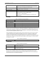
1
PCI-DAS4020/12 Analog & Digital I/O Board User’s Guide Document Revision 8, June, 2006 © Copyright 2006, Measurement Computing Corporation Your new Measurement Computing product comes with a fantastic extra — Management committed to your satisfaction! Refer to www.mccdaq.com/execteam.html for the names, titles, and contact information of each key executive at Measurement Computing. Thank you for choosing a Measurement Computing product—and congratulations! You own the finest, and you can now enjoy the protection of the most comprehensive warranties and unmatched phone tech support. It’s the embodiment of our two missions: ! To offer the highest-quality, computer-based data acquisition, control, and GPIB hardware and software available—at the best possible price. ! To offer our customers superior post-sale support—FREE. Whether providing unrivaled telephone technical and sales support on our latest product offerings, or continuing that same first-rate support on older products and operating systems, we’re committed to you! Lifetime warranty: Every hardware product manufactured by Measurement Computing Corporation is warranted against defects in materials or workmanship for the life of the product. Products found defective are repaired or replaced promptly. Lifetime Harsh Environment Warranty®: We will replace any product manufactured by Measurement Computing Corporation that is damaged (even due to misuse) for only 50% of the current list price. I/O boards face some tough operating conditionssome more severe than the boards are designed to withstand. When a board becomes damaged, just return the unit with an order for its replacement at only 50% of the current list price. We don’t need to profit from your misfortune. By the way, we honor this warranty for any manufacturer’s board that we have a replacement for. 30 Day Money Back Guarantee: You may return any Measurement Computing Corporation product within 30 days of purchase for a full refund of the price paid for the product being returned. If you are not satisfied, or chose the wrong product by mistake, you do not have to keep it. Please call for an RMA number first. No credits or returns accepted without a copy of the original invoice. Some software products are subject to a repackaging fee. These warranties are in lieu of all other warranties, expressed or implied, including any implied warranty of merchantability or fitness for a particular application. The remedies provided herein are the buyer’s sole and exclusive remedies. Neither Measurement Computing Corporation, nor its employees shall be liable for any direct or indirect, special, incidental or consequential damage arising from the use of its products, even if Measurement Computing Corporation has been notified in advance of the possibility of such damages. HM PCI-DAS4020-12.doc ii Trademark and Copyright Information TracerDAQ, Universal Library, Harsh Environment Warranty, Measurement Computing Corporation, and the Measurement Computing logo are either trademarks or registered trademarks of Measurement Computing Corporation. Windows, Microsoft, and Visual Studio are either trademarks or registered trademarks of Microsoft Corporation LabVIEW is a trademark of National Instruments. CompactFlash is a registered trademark of SanDisk Corporation. All other trademarks are the property of their respective owners. Information furnished by Measurement Computing Corporation is believed to be accurate and reliable. However, no responsibility is assumed by Measurement Computing Corporation neither for its use; nor for any infringements of patents or other rights of third parties, which may result from its use. No license is granted by implication or otherwise under any patent or copyrights of Measurement Computing Corporation. All rights reserved. No part of this publication may be reproduced, stored in a retrieval system, or transmitted, in any form by any means, electronic, mechanical, by photocopying, recording, or otherwise without the prior written permission of Measurement Computing Corporation. Notice Measurement Computing Corporation does not authorize any Measurement Computing Corporation product for use in life support systems and/or devices without prior written consent from Measurement Computing Corporation. Life support devices/systems are devices or systems which, a) are intended for surgical implantation into the body, or b) support or sustain life and whose failure to perform can be reasonably expected to result in injury. Measurement Computing Corporation products are not designed with the components required, and are not subject to the testing required to ensure a level of reliability suitable for the treatment and diagnosis of people. iii Table of Contents Preface About this User's Guide ......................................................................................................................vi What you will learn from this user's guide ........................................................................................................vi Conventions in this user's guide ........................................................................................................................vi Where to find more information ........................................................................................................................vi Chapter 1 Introducing the PCI-DAS4020/12 ..................................................................................................... 1-1 Overview: PCI-DAS4020/12 features ............................................................................................................ 1-1 Software features ............................................................................................................................................ 1-1 Chapter 2 Installing the PCI-DAS4020/12 ......................................................................................................... 2-1 What comes with your PCI-DAS4020/12 shipment? ..................................................................................... 2-1 Hardware ....................................................................................................................................................................... 2-1 Additional documentation.............................................................................................................................................. 2-1 Optional components ..................................................................................................................................................... 2-1 Unpacking the PCI-DAS4020/12 ................................................................................................................... 2-2 Installing the software .................................................................................................................................... 2-2 Installing the PCI-DAS4020/12...................................................................................................................... 2-2 Configuring the PCI-DAS4020/12 ................................................................................................................. 2-2 Connecting the board for I/O operations ........................................................................................................ 2-3 Connectors, cables – I/O connectors .............................................................................................................................. 2-3 BNC connectors............................................................................................................................................................. 2-3 Pin out – auxiliary connector ......................................................................................................................................... 2-4 Cabling........................................................................................................................................................................... 2-4 Field wiring, signal termination and conditioning ......................................................................................................... 2-7 Chapter 3 Programming and Developing Applications .................................................................................. 3-1 Programming languages ................................................................................................................................. 3-1 Packaged applications programs..................................................................................................................... 3-1 Register level programming ........................................................................................................................... 3-1 Chapter 4 Functional Details ............................................................................................................................. 4-1 PCI-DAS4020/12 block diagram.................................................................................................................... 4-1 Analog input signal path................................................................................................................................. 4-1 Analog output ................................................................................................................................................. 4-2 Digital I/O....................................................................................................................................................... 4-2 Power distribution........................................................................................................................................... 4-2 Input impedance configuration ....................................................................................................................... 4-2 Chapter 5 Calibrating the PCI-DAS4020/12 ...................................................................................................... 5-1 Calibration theory ........................................................................................................................................... 5-1 Chapter 6 Specifications.................................................................................................................................... 6-1 Analog input ................................................................................................................................................... 6-1 iv PCI-DAS4020/12 User's Guide Timing and throughput .................................................................................................................................................. 6-1 Accuracy ........................................................................................................................................................................ 6-2 Temperature................................................................................................................................................................... 6-2 Dynamics and noise ....................................................................................................................................................... 6-3 Trig/Ext Clk BNC........................................................................................................................................... 6-3 Analog output ................................................................................................................................................. 6-3 Accuracy ........................................................................................................................................................................ 6-4 Digital input / output....................................................................................................................................... 6-4 Interrupts......................................................................................................................................................... 6-4 Environmental ................................................................................................................................................ 6-5 Power consumption ........................................................................................................................................ 6-5 Connector and pin out..................................................................................................................................... 6-5 Auxiliary connector P3 pinout ....................................................................................................................................... 6-5 v Preface About this User's Guide What you will learn from this user's guide This user's guide explains how to install, configure, and use the PCI-DAS4020/12 so that you get the most out of its analog and digital I/O features. This user's guide also refers you to related documents available on our web site, and to technical support resources. Conventions in this user's guide For more information on … Text presented in a box signifies additional information and helpful hints related to the subject matter you are reading. Caution! Shaded caution statements present information to help you avoid injuring yourself and others, damaging your hardware, or losing your data. <#:#> Angle brackets that enclose numbers separated by a colon signify a range of numbers, such as those assigned to registers, bit settings, etc. bold text Bold text is used for the names of objects on the screen, such as buttons, text boxes, and check boxes. For example: 1. Insert the disk or CD and click the OK button. italic text Italic text is used for the names of manuals and help topic titles, and to emphasize a word or phrase. For example: The InstaCal installation procedure is explained in the Quick Start Guide. Never touch the exposed pins or circuit connections on the board. Where to find more information The following electronic documents provide information that can help you get the most out of your PCIDAS4020/12. ! ! ! ! ! ! MCC's Specifications: PCI-DAS4020/12 (the PDF version of the Specifications chapter in this guide) is available on our web site at www.mccdaq.com/pdfs/pci-das4020_12.pdf. MCC's Quick Start Guide is available on our web site at www.mccdaq.com/PDFmanuals/DAQ-Software-Quick-Start.pdf. MCC's Guide to Signal Connections is available on our web site at www.mccdaq.com/signals/signals.pdf. MCC's Universal Library User's Guide is available on our web site at www.mccdaq.com/PDFmanuals/sm-ul-user-guide.pdf. MCC's Universal Library Function Reference is available on our web site at www.mccdaq.com/PDFmanuals/sm-ul-functions.pdf. MCC's Universal Library for LabVIEW™ User’s Guide is available on our web site at www.mccdaq.com/PDFmanuals/SM-UL-LabVIEW.pdf. PCI-DAS4020/12 User's Guide (this document) is also available on our web site at www.mccdaq.com/PDFmanuals/pci-das4020-12.pdf. vi Chapter 1 Introducing the PCI-DAS4020/12 Overview: PCI-DAS4020/12 features This manual explains how to install and use the PCI-DAS4020/12 board. The PCI-DAS4020/12 is a multi-function high-speed data acquisition I/O board that is designed for the PCI bus. It provides the following features: ! ! ! Four high-speed 12-bit analog input channels The input range for each channel is software-configurable for ±1 V or ±5 V. The sample rate is from 10 to 20 MHz, depending on the number of channels accessed. Triggering sources and A/D gating are via hardware or software, and can be internal or external. Four different modes are software selectable. Analog input connectors are standard BNC types. Two 12-bit analog output channels Each analog output channel can be configured by software for an output range of ±10 V or ±5 V. Throughput is system-dependent. Triggering mode is software gate. D/A pacing is software paced. The analog output channels terminate at a 40-pin auxiliary connector. 24 digital I/O channels An on-board industry standard 82C55A I/O chip provides 24 digital I/O channels configured as two banks of eight and two banks of four. You can configure each bank independently as input or output. Signal levels are TTL. The digital I/O channels terminate at a 40-pin auxiliary connector. Software features For information on the features of InstaCal and the other software included with your PCI-DAS4020/12, refer to the Quick Start Guide that shipped with your device. The Quick Start Guide is also available in PDF at www.mccdaq.com/PDFmanuals/DAQ-Software-Quick-Start.pdf. Check www.mccdaq.com/download.htm for the latest software version or versions of the software supported under less commonly used operating systems. 1-1 Chapter 2 Installing the PCI-DAS4020/12 What comes with your PCI-DAS4020/12 shipment? The following items are shipped with the PCI-DAS4020/12. Hardware ! PCI-DAS4020/12 Additional documentation In addition to this hardware user's guide, you should also receive the Quick Start Guide (available in PDF at www.mccdaq.com/PDFmanuals/DAQ-Software-Quick-Start.pdf). This booklet supplies a brief description of the software you received with your PCI-DAS4020/12 and information regarding installation of that software. Please read this booklet completely before installing any software or hardware. Optional components If you ordered any of the following products with your board, they should be included with your shipment. ! Cables C40FF-x C40-37F-x BP40-37F-x Signal termination and conditioning accessories MCC provides signal termination products for use with the PCI-DAS4020/12. Refer to the "Field wiring, signal termination and conditioning" section on page 2-7 for a complete list of compatible accessory products. 2-1 PCI-DAS4020/12 User's Guide Installing the PCI-DAS4020/12 Unpacking the PCI-DAS4020/12 As with any electronic device, you should take care while handling to avoid damage from static electricity. Before removing the PCI-DAS4020/12 from its packaging, ground yourself using a wrist strap or by simply touching the computer chassis or other grounded object to eliminate any stored static charge. If any components are missing or damaged, notify Measurement Computing Corporation immediately by phone, fax, or e-mail: ! ! ! Phone: 508-946-5100 and follow the instructions for reaching Tech Support. Fax: 508-946-9500 to the attention of Tech Support Email: [email protected] Installing the software Refer to the Quick Start Guide for instructions on installing the software on the Measurement Computing Data Acquisition Software CD. This booklet is available in PDF at www.mccdaq.com/PDFmanuals/DAQ-SoftwareQuick-Start.pdf. Installing the PCI-DAS4020/12 The PCI-DAS4020/12 board is completely plug-and-play, with no switches or jumpers to set. Configuration is controlled by your system's BIOS. To install your board, follow the steps below. Install the MCC DAQ software before you install your board The driver needed to run your board is installed with the MCC DAQ software. Therefore, you need to install the MCC DAQ software before you install your board. Refer to the Quick Start Guide for instructions on installing the software. 1. Turn your computer off, open it up, and insert your board into an available PCI slot. 2. Close your computer and turn it on. If you are using an operating system with support for plug-and-play (such as Windows 2000 or Windows XP), a dialog box opens as the system loads, indicating that new hardware has been detected. If the information file for this board is not already loaded onto your PC, you are prompted for the disk containing this file. The Measurement Computing Data Acquisition Software CD supplied with your board contains this file. If required, insert the disk or CD and click OK. 3. To test your installation and configure your board, run the InstaCal utility installed in the previous section. Refer to the Quick Start Guide that came with your board for information on how to initially set up and load InstaCal. If your board has been powered-off for more than 10 minutes, allow your computer to warm up for at least 15 minutes before acquiring data. This warm-up period is required in order for the board to achieve its rated accuracy. The high speed components used on the board generate heat, and it takes this amount of time for a board to reach steady state if it has been powered off for a significant amount of time. Configuring the PCI-DAS4020/12 All of the hardware configuration options on the PCI-DAS4020/12 are software controlled. Use InstaCal to select the number of channels to sample (one, two or four channels), and the analog output range (±10 V or ±5 V.) Once selected, any program that uses the Universal Library will initialize the hardware according to your selections. 2-2 PCI-DAS4020/12 User's Guide Installing the PCI-DAS4020/12 Connecting the board for I/O operations Connectors, cables – I/O connectors Table 2-1 lists the board connectors, applicable cables, and compatible accessory products for the PCIDAS4020/12. Table 2-1. Board connectors, cables, compatible hardware Connector type Compatible cables (for the 40-pin auxiliary connector) Compatible accessory products with the C40FF-x cable Compatible accessory products with the C40-37F-x cable or with the BP40-37-x and the C37FF-x or C37FFS-x cable ! BNC connector: five standard female connectors ! Auxiliary connector (P3): 40-pin header connector ! C40FF-x ! C40-37F-x ! BP40-37-x CIO-MINI40 ! ! ! ! ! ! CIO-MINI37 SCB-37 CIO-ERB24 CIO-ERB08 SSR-RACK24 SSR-RACK08 Information on signal connections General information regarding signal connection and configuration is available in the Guide to Signal Connections. This document is available on our web site at http://www.measurementcomputing.com/signals/signals.pdf. BNC connectors The board’s analog input and trigger input connectors are standard female BNC connectors that are visible from the rear of the computer when you install the board. Channel 0 Channel 1 Channel 2 Channel 3 TRIG /Ext Clk Figure 2-1. Analog inputs and trigger input BNC connectors 2-3 PCI-DAS4020/12 User's Guide Installing the PCI-DAS4020/12 Pin out – auxiliary connector Table 2-2 defines the pin out for the board’s 40-pin on-board auxiliary connector (labeled P3 on the board). Pin 1 is identified by a beveled edge on the board silkscreen. Table 2-2. 40-pin auxiliary connector P3 Signal Name D/A OUT 1 D/A GND FIRSTPORTA Bit 0 FIRSTPORTA Bit 1 FIRSTPORTA Bit 2 FIRSTPORTA Bit 3 FIRSTPORTA Bit 4 FIRSTPORTA Bit 5 FIRSTPORTA Bit 6 FIRSTPORTA Bit 7 FIRSTPORTC Bit 0 FIRSTPORTC Bit 1 FIRSTPORTC Bit 2 FIRSTPORTC Bit 3 FIRSTPORTC Bit 4 FIRSTPORTC Bit 5 (Start Trigger In/Ext Clock) FIRSTPORTC Bit 6 (A/D Stop Trigger In) FIRSTPORTC Bit 7 (A/D Pacer Gate) GND +5V PCI slot Pin 40 38 36 34 32 30 28 26 24 22 20 18 16 14 12 10 8 6 4 2 •• •• •• •• •• •• •• •• •• •• •• •• •• •• •• •• •• •• •• •• Pin 39 37 35 33 31 29 27 25 23 21 19 17 15 13 11 9 7 5 3 1 Signal Name D/A OUT 0 GND +5V GND n/c GND n/c GND n/c GND FIRSTPORTB Bit 0 FIRSTPORTB Bit 1 FIRSTPORTB Bit 2 FIRSTPORTB Bit 3 FIRSTPORTB Bit 4 FIRSTPORTB Bit 5 FIRSTPORTB Bit 6 FIRSTPORTB Bit 7 INTERRUPT ENABLE * INTERRUPT IN * ↓ * Pin 1 and pin 3 have 10 K pull-up resistors installed. Use pin 38 for analog output return When using the analog output pins D/A OUT 0 (pin 39) and D/A OUT 1 (pin 40), use D/A GND only (pin 38) for the return. Cabling For signal connections and termination, you can use the CIO-MINI40 screw terminal board and C40FF-x cable. For connections to 37-pin screw terminal boards, you can use the C40-37F-x cable. 2 40 1 The red stripe identifies pin # 1 2 40 39 40-pin Female IDC Connector 1 39 40-pin Female IDC Connector Figure 2-2. C40FF-x cable 2-4 PCI-DAS4020/12 User's Guide 2 Installing the PCI-DAS4020/12 The red stripe identifies pin # 1 1 1 20 37 40 19 39 40-pin Female IDC Connector 37-pin Female Dsub Connector Figure 2-3. C40-37F-x cable If you don’t need to connect to the PCI-DAS4020/12 analog outputs (pins 38 to 40), you can connect to a BP40-37 cable. The BP40-37 cable brings pins 1 through 37 of the 40-pin connector out to 37-pin male "D" connector mounted on a backplane bracket. 19 39 40 1 2 37 Key 20 1 The red stripe and arrow identify pin # 1 37-pin Male D Connector with Backplate Assembly 40-pin Female IDC Connector Figure 2-4. BP40-37 cable 2-5 PCI-DAS4020/12 User's Guide Installing the PCI-DAS4020/12 GND FIRSTPORTA BIT 0 FIRSTPORTA BIT 1 FIRSTPORTA BIT 2 FIRSTPORTA BIT 3 FIRSTPORTA BIT 4 FIRSTPORTA BIT 5 FIRSTPORTA BIT 6 FIRSTPORTA BIT 7 FIRSTPORTC BIT 0 FIRSTPORTC BIT 1 FIRSTPORTC BIT 2 FIRSTPORTC BIT 3 FIRSTPORTC BIT 4 FIRSTPORTC BIT 5 FIRSTPORTC BIT 6 FIRSTPORTC BIT 7 GND +5V +5V GND NC GND NC GND NC GND FIRSTPORTB BIT 1 FIRSTPORTB BIT 2 FIRSTPORTB BIT 3 FIRSTPORTB BIT 4 FIRSTPORTB BIT 5 FIRSTPORTB BIT 6 FIRSTPORTB BIT 7 NC Figure 2-5. BP40-37 cable pin out 40-pin to 37-pin signal mapping Signal mapping on the C40-37F-x and the BP40-37 cables is not 1:1. Table 2-3 lists the pin numbers of the signals on the 40-pin end and the pin numbers of the associated signals on the 37-pin end. Table 2-3. Signal mapping on the C40-37F-x and BP40-37F cables Pin 1 2 3 4 5 6 7 8 9 10 11 12 13 14 15 16 17 18 19 20 21 22 23 24 25 26 40-pin cable end Signal Name INTERRUPT IN +5V INTERRUPT ENABLE GND Port B 7 Port C 7 Port B 6 Port C 6 Port B 5 Port C 5 Port B 4 Port C 4 Port B 3 Port C 3 Port B 2 Port C 2 Port B 1 Port C 1 Port B 0 Port C 0 GND Port A 7 N/C Port A 6 GND Port A 5 Pin 1 20 2 21 3 22 4 23 5 24 6 25 7 26 8 27 9 28 10 29 11 30 12 31 13 32 2-6 37-pin cable end Signal Name INTERRUPT IN +5V INTERRUPT ENABLE GND Port B 7 Port C 7 Port B 6 Port C 6 Port B 5 Port C 5 Port B 4 Port C 4 Port B 3 Port C 3 Port B 2 Port C 2 Port B 1 Port C 1 Port B 0 Port C 0 GND Port A 7 N/C Port A 6 GND Port A 5 PCI-DAS4020/12 User's Guide Pin 27 28 29 30 31 32 33 34 35 36 37 38 39 40 Installing the PCI-DAS4020/12 40-pin cable end Signal Name N/C Port A 4 GND Port A 3 N/C Port A 2 GND Port A 1 +5V Port A 0 GND N/C N/C N/C Pin 14 33 15 34 16 35 17 36 18 37 19 37-pin cable end Signal Name N/C Port A 4 GND Port A 3 N/C Port A 2 GND Port A 1 +5V Port A 0 GND For digital signal conditioning, you can connect the BP40-37 cable to a C37FF-x or C37FFS- x cable, and then connect one of these cables to the 37-pin connector on MCC’s digital signal conditioning boards. Refer to page 2-8 for a list of compatible boards. The red stripe identifies pin # 1 1 1 20 20 37 37 19 19 Figure 2-6. C37FF-x cable 1 19 1 20 37 19 20 37 Figure 2-7. C37FFS-x cable Field wiring, signal termination and conditioning You can use the following MCC screw terminal board to terminate field signals and route them into the PCIDAS4020/12 board using the C40FF-x cable: ! CIO-MINI40 – 40-pin universal screw terminal board. Details are available on our web site at www.mccdaq.com/cbicatalog/cbiproduct.asp?dept_id=102&pf_id=257. You can use the following MCC screw terminal boards to terminate field signals and route them into the PCIDAS4020/12 board using the C40-37F-x cable directly or by combining the BP40-37-x cable with the C37FF-x or C37FFS-x cable: ! ! CIO-MINI37 – 37-pin universal screw terminal board. Details are available on our web site at www.mccdaq.com/cbicatalog/cbiproduct.asp?dept_id=102&pf_id=255. SCB-37 – 37 conductor, shielded signal connection/screw terminal box. Details on are available on our web site at www.mccdaq.com/cbicatalog/cbiproduct.asp?dept_id=196&pf_id=1166. 2-7 PCI-DAS4020/12 User's Guide Installing the PCI-DAS4020/12 Digital Signal Conditioning For digital signal conditioning, you can connect the PCI-DAS4020/12 to the following boards using the C4037F-x cable directly or by combining the BP40-37-x cable with the C37FF-x or C37FFS-x cable. ! ! ! ! CIO-ERB24 – 24 Form C, 6A relays. Details on this product are available on our web site at www.mccdaq.com/cbicatalog/cbiproduct.asp?dept_id=123&pf_id=241. CIO-ERB08 – Eight Form C, 6A relays. Details are available on our web site at www.mccdaq.com/cbicatalog/cbiproduct.asp?dept_id=123&pf_id=240. SSR-RACK24 – 24-channel solid state module rack. Details are available on our web site at www.mccdaq.com/cbicatalog/cbiproduct.asp?dept_id=122&pf_id=1193. SSR-RACK08 – 24-channel solid state module rack. Details are available on our web site at www.mccdaq.com/cbicatalog/cbiproduct.asp?dept_id=122&pf_id=620. 2-8 Chapter 3 Programming and Developing Applications After following the installation instructions, your PCI-DAS4020/12 is ready for use. Although the board is part of the larger DAS family, there is no correspondence between registers. Software written at the register level for other DAS models will not work with the PCI-DAS4020/12. Programming languages Measurement Computing’s Universal Library® provides access to board functions from a variety of Windows programming languages. If you are planning to write programs, or would like to run the example programs for Visual Basic or any other language, please refer to the Universal Library User's Guide (available on our web site at www.mccdaq.com/PDFmanuals/sm-ul-user-guide.pdf). Packaged applications programs Many packaged application programs, such as SoftWIRE and HP-VEE™, now have drivers for your board. If the package you own does not have drivers for the board, please fax or e-mail the package name and the revision number from the install disks. We will research the package for you and advise how to obtain drivers. Some application drivers are included with the Universal Library package, but not with the application package. If you have purchased an application package directly from the software vendor, you may need to purchase our Universal Library and drivers. Please contact us by phone, fax or e-mail: ! ! ! Phone: 508-946-5100 and follow the instructions for reaching Tech Support. Fax: 508-946-9500 to the attention of Tech Support Email: [email protected] Register level programming You should use the Universal Library or one of the packaged application programs mentioned above to control your board. Only experienced programmers should try register-level programming. To program at the register level in your application, refer to the Register Map for the PCI-DAS4020/12 Series (available at www.mccdaq.com/registermaps/RegMapPCI-DAS4020-12.pdf. 3-1 Chapter 4 Functional Details PCI-DAS4020/12 block diagram PCI-DAS4020/12 functions are illustrated in the block diagram shown here. Four analog input channels per board Attenuator/ Amplifier ADC Input MUX BNC IN VREF CONV 50 OhmS BNC 12 Gain & Offset AUTOCAL External Pacer TRIG1, TRIG2, or GATE System Timing Controller Analog Clock/ Trigger Analog Outputs Dual12-bit DAC 24 I/O Digital I/0 (82C55) Four Channels Local Bus Dual 32K x 24 SRAM PC Bus Controller PCI Bus Connector (5V, 32 BIT, 33 MHZ) Figure 4-1. PCI-DAS4020/12 Block Diagram Analog input signal path Four single-ended analog input channels, connect from BNC connectors to individual amplifiers and then connect to dedicated ADC’s. Each path allows for: ! ! ! 50 ohm or high-Z termination, selected by solder gap ±1 V or ±5 V bipolar ranges, software-selectable (see Table 4-1) Auto-calibration for offset and gain adjustments for each channel and each range Table 4-1. Input range Full Scale Input Range Attenuation Divider Output +5 V to -5 V 5 ±1 V +1 V to -1 V 1 ±1 V 4-1 PCI-DAS4020/12 User's Guide Functional Details Analog output Two 12-bit voltage outputs are software programmable for ±10 V or ±5 V. The D/A is the Analog Devices AD7237 Dual DAC. Since the DAC is dual buffered, the DAC output voltage is updated after the MS nibble is written to the DAC. The DACs initially power-up and are reset to 0 V. There is no calibration on these DACs. The offset and gain errors are minimized by using precision components. Table 4-2 shows the DAC input coding. Table 4-2. DAC input coding DAC Range Input Code Binary 12 bit Input Code Hex 12 bit Output Voltage −10.000 V 0V ± 10 V 0000 0000 0000 000h ± 10 V 1000 0000 0000 800h ± 10 V 1111 1111 1111 FFFh +9.99513 V ±5V 0000 0000 0000 000h ±5V 1000 0000 0000 800h −5.000 V 0V ±5V 1111 1111 1111 FFFh +4.99756 V Figure 4-2. Analog output block diagram Digital I/O The digital I/O is an 82C55 digital logic device. An external interrupt source pin (pin 1) and external interrupt enable pin (pin 3) on the auxiliary 40-pin connector (P3) are used for external interrupts. These lines are pulled up and an OR operation is performed on them to generate the external interrupt signal. Both are active low. Power distribution The PCI-DAS4020/12 board is powered by the PCI bus. The only power used is +5 V. Input impedance configuration Each analog input and the trigger/clock input channel on the PCI-DAS4020/12 has a dedicated solder gap. A solder gap consists of two copper pads that you can solder together to change the input impedance of the channel. When the solder gaps are open (default), the input impedance is 1.5 MΩ. When the solder gaps are closed, the input impedance is 50 Ω. To close the solder gaps and change the impedance to 50 ohm, solder the two copper pads together. To close the solder gap, touch a soldering iron to the two contacts until some rosin core solder flows across the copper pads and forms a small blob of solder. Be careful not to overheat the pads, or they may delaminate from the circuit board. Do not add too much solder, as it could flow onto other components and cause an electrical short or other defect. 4-2 PCI-DAS4020/12 User's Guide Functional Details Solder Gap Configuration Input Impedance Open Close 1.5 MΩ typical 50 Ω The board designation for the analog input channels and the trigger/clock BNC input are listed below. Solder Gap board label Channel SG1 SG2 SG3 SG4 SG5 Channel 0 Channel 1 Channel 2 Channel 3 TRIG/Ext Clock input Solder gaps for the analog input channels are located on the rear of the board (circuit-side) and are labeled SG1 to SG4. See Figure 4-3. Figure 4-3. Analog input channel solder gap locations (circuit-side) The solder gap for the trigger/clock input is located on the front of the board (component-side) and is labeled SG5. See Figure 4-4. Figure 4-4. Trigger/clock input solder gap location (component-side) 4-3 PCI-DAS4020/12 User's Guide Functional Details An example of each input impedance configuration option is shown in Figure 4-5. Solder gap SG3 is open (1.5 Mohms) Solder gap SG4 is closed (50 ohms) Figure 4-5. Open and closed solder gaps 4-4 Chapter 5 Calibrating the PCI-DAS4020/12 Use the InstaCal utility program to calibrate the PCI-DAS4020/12. InstaCal calibrates the PCI-DAS4020/12 using on-board digital potentiometers and trim D/A converters. No external equipment or user adjustments are required. The PCI-DAS4020/12 is factory calibrated. The calibration coefficients are stored in nvRAM. Analog input adjustments are made via 10-bit calibration DACs that are referenced to the on-board factory calibrated standard. Each channel has a pair of dedicated 10-bit DACs that trim out offset and gain errors. InstaCal calibrates the offset by adjusting the offset voltage at the input of each ADC, and adjusts the gain via the ADC reference pin. At run time, the calibration factors are loaded into system memory and are automatically retrieved each time a different ADC range is specified. You can recalibrate any time using factory voltage standards with InstaCal. A full calibration typically takes less than two minutes. Before you calibrate the board, turn your computer on and allow at least 30 minutes for the internal case temperature to stabilize. For best results, calibrate the board immediately before making critical measurements. The high resolution analog components on the board are sensitive to temperature. Pre-measurement calibration insures that your board is operating with optimum calibration values. Calibration theory Analog inputs are calibrated for offset and gain. Offset calibration is performed directly on the input amplifier, with coarse and fine trim DACs acting on the amplifier. For input gain calibration, a precision calibration reference is used in conjunction with coarse and fine trim DACs acting on the ADC. See Figure 5-1. Analog In Gain Calibration Reference ADC MUX Gain Adjust Offset Adjust Trim DAC Coarse Trim DAC Fine Trim DAC Coarse Trim DAC Fine Figure 5-1. Analog input calibration 5-1 Chapter 6 Specifications Typical for 25 °C unless otherwise specified. Specifications in italic text are guaranteed by design. Analog input Table 1. Analog input specifications A/D converter type Resolution Programmable ranges Number of channels Connection Bandwidth Coupling Input leakage current Input impedance AD9225, 25 MSPS pipelined A/D 12-bits ±5 V, ±1 V 4 single-ended, independent ADC’s per channel 4 independent BNC 17 MHz typical DC 2 uA typ, 10 uA max 1.5 Mohm typ, or 50 ohm, selectable (coaxial cable termination) ±15 V Absolute maximum input voltage Timing and throughput Table 2. Timing and throughput specifications Simultaneous sampling A/D Convert clock source A/D Gate source A/D Gate modes A/D Start Trigger (TRIG1) A/D Stop Trigger (TRIG2) A/D Triggering modes Software selectable option - 1, 2, or 4 channels Internal: ! On-card crystal oscillator ! Frequency: 40 MHz ! Frequency accuracy: 50% duty cycle, 50 ppm External: ! Trig/Ext Clk BNC, or A/D External Clock on the 40-pin connector ! 24-bit internal pre-scale counter (min pre-scale = 2) ! Clock Rate: 40 MHz max, 2 kHz min ! Duty Cycle: 50% ± 5% Digital: Trig/Ext Clk BNC or A/D Pacer Gate on 40-pin connector Analog: Any of the four input channels Digital: Programmable active high/low, level/edge Analog: Above/below reference, positive/negative Hysteresis, inside/outside window Resolution: 12-bit Slew rate: 10V/sec. minimum Software: Using a DAQ start command. Digital: Trig/Ext Clk BNC, A/D Start Trigger In (on the 40-pin connector) Analog: Any of the four input channels Digital: Trig/Ext Clk BNC, A/D Stop Trigger In (on the 40-pin connector) Analog: Any of the four input channels Digital: Programmable rising or falling edge Analog: Trigger above/below reference Resolution: 12-bit 6-1 PCI-DAS4020/12 User's Guide Pre-trigger mode Data transfer A/D Conversion time Sample rate Throughput Specifications Unlimited number of pre-trigger samples, 16 Meg post-trigger samples. Compatible with both digital and analog trigger/gate options. Data acquisition initiated via TRIG1. Post-trigger phase initiated via TRIG2. Via dual 32 K x 24 sample FIFO, SRAM based, with Bus-Master DMA and scatter-gather, interrupt, or software polled. 40 ns 20 MHz max, 1 kHz min Single channel: 20 MHz continuous Two channels (0 and 1 or 2 and 3): 20 MHz continuous Four channels: 10 MHz continuous In background mode, the maximum throughput may be impacted by bus or interrupt activity. Accuracy Table 3. Analog input accuracy specifications Absolute accuracy Typical accuracy ±5.5 LSB worst case error (either range) ±3.0 LSB error (either range) Accuracy components: Gain error Offset error Integral linearity error Differential linearity error ±2.0 LSB max, ±1.0 LSB typ ±1.5 LSB max, ±1.0 LSB typ ±2.5 LSB max, ±1.0 LSB typ ±1.0 LSB max , ±0.4 LSB typ (No missing codes guaranteed) Board error is a combination of gain, offset, integral linearity, and differential linearity error. The overall absolute worst-case error of the board may be calculated by summing these component errors. Worst case error is realized only in the unlikely event that each of the component errors are both at their maximum level, and causing error in the same direction. Though this is very uncommon, it is still possible, and the calculated worst case error of the PCI-DAS4020/12 board is ±7.0 LSB. Each PCI-DAS4020/12 board is tested at the factory to make sure that its actual worst case error is less than ±5.0 LSB. Allowing for a 10% guard-band, the absolute worst-case error of a board is ±5.5 LSB. Typical accuracy can be calculated from the various component typical errors in a similar fashion. This typical maximum error calculation for the PCI-DAS4020/12 board yields ±3.4 LSB. However, this again assumes that each of the errors is forcing an error in the same direction. Empirical evidence supports a conservative typical error budget of ±3.0 LSB. Table 4. Calibration specifications Calibration Auto-calibration. Calibration factors for each range stored on board in non-volatile RAM Temperature Table 5. Temperature specifications Gain drift Offset drift Overall board temperature drift ±5 V range: ±0.10 LSB/°C max ±1 V range: ±0.13 LSB/°C max ±0.11 LSB/°C max, all ranges ±5 V range: ±0.21 LSB/°C max ±1 V range: ±0.24 LSB/°C max Overall, worst-case temperature drift is calculated by adding the drifts corresponding to the gain and offset drifts. This worst case number is unlikely to occur, as it requires both gain and offset drifts to be at their maximum levels, and to be affecting the measurement in the same direction. However, the overall board D/A drift specifications have been calculated in this fashion. 6-2 PCI-DAS4020/12 User's Guide Specifications Dynamics and noise Table 6. Dynamics and noise specifications SNR (Signal-to-noise ratio) SINAD (signal-to-noise and distortion ratio) SFDR (spurious free dynamic range) THD (total harmonic distortion) Noise distribution: (Rate = 10 KHz-20 MHz, Average % ± 2 bins, Average % ± 1 bin, Average # bins) 66.6 dB 66.5 dB 80 dB 80 dB Bipolar (5V): Bipolar (1V): 100% / 98% / 5 bins 100% / 98% / 5 bins Trig/Ext Clk BNC Software selectable for A/D Start Trigger (TRIG1), A/D Stop Trigger (TRIG2) or A/D Pacer Gate (AGATE); also used as an A/D clock input 2X clock source (DAQ_CLK). Table 7. Trig/Ext Clk BNC specifications Input impedance Input threshold Input slew rate Input range Bandwidth Coupling 50 ohm, 1 Mohm selectable (coaxial cable termination) Programmable 2.5 V threshold or 0 V threshold 1 V/µsec min ±5 V 40 MHz DC Analog output Table 8. Analog output specifications D/A converter type Resolution Number of channels Output range D/A pacing Throughput Data transfer Monotonicity Analog output drift Settling time (20 V step to ± ½ LSB) Slew rate Current drive Output short-circuit duration Output coupling Output impedance AD7237 12-bits 2 ±10 V, ±5 V software selectable Software paced System dependent. Using the Universal Library programmed output function (cbAout) in a loop in Visual Basic, a typical update rate of 500 Hz (± 50 Hz) can be expected. The rate was measured on a 330 MHz Pentium II based PC. Programmed I/O Guaranteed monotonic over temperature ±0.11 LSB/°C max, all ranges 5 µs max 5 V/µs ±5 mA 25 mA indefinite DC 0.5 Ohm max 6-3 PCI-DAS4020/12 User's Guide Miscellaneous Specifications ! Single buffered output latch ! Update DACs individually On power-up and reset, the inputs to both D/A output buffers are grounded and the board’s D/A outputs will be set to 0 volts ± 6 mV. Upon writing to the D/A converters, the output buffers will reflect the D/A outputs and achieve rated accuracy. However, upon writing a 0 to the D/A’s, a small output change may be noted (up to 10 LSB). Accuracy Table 9. Analog output accuracy specifications Absolute accuracy Offset error Gain error Differential non-linearity Integral non-linearity ±13 LSB max ±6 LSB max ±5 LSB max ±1 LSB max ±1 LSB max Total analog output error is a combination of gain, offset, integral linearity, and differential linearity error. The overall absolute worst-case error of the board may be calculated by summing these component errors. Worst case error is realized only in the unlikely event that each of the component errors are both at their maximum level, and causing error in the same direction. Though this is very uncommon, it is still possible. Digital input / output Table 10. DIO specifications Digital type (40-pin connector) Configuration Number of channels Output high Output low Input high Input low Power-up / reset state 8255A 2 banks of 8, 2 banks of 4, programmable by bank as input or output 24 I/O 3.0 volts min @ 2.5 mA 0.4 volts max @ 2.5 mA 2.0 volts min, Vcc + 0.5 volts absolute max 0.8 volts max, GND − 0.5 volts absolute min Input mode (high impedance) Interrupts Table 11. Interrupt specifications Interrupts Interrupt enable ADC Interrupt sources External External Interrupt Enable INTA# - mapped to IRQn via PCI BIOS at boot-time Software programmable DAQ_ACTIVE: Interrupt is generated when a DAQ sequence is active. DAQ_STOP: Interrupt is generated when A/D Stop Trigger In is detected. DAQ_DONE: Interrupt is generated when a DAQ sequence completes. DAQ_FIFO_1/2_FULL: Interrupt is generated when ADC FIFO is ½ full. DAQ_SINGLE: Interrupt is generated after each conversion completes. Interrupt is generated via edge-sensitive transition on the Interrupt In pin on the 40-pin connector. Rising/falling edge polarity selection. The Interrupt In pin is pulled up to 5 V through a 10 K resistor. Active low Interrupt Enable signal on the 40-pin connector. The Interrupt Enable pin is pulled up to 5 V through a 10 K resistor. 6-4 PCI-DAS4020/12 User's Guide Specifications Environmental Table 12. Environmental specifications Operating temperature range Storage temperature range Humidity 0 to 70 °C −40 to 100 °C 0 to 90% non-condensing Power consumption Table 13. Power consumption specifications +5 V Operating (A/D to FIFO) 1.5 A typical, 2.0 A max Connector and pin out Table 14. Connector specifications Connector type Compatible cables (for the 40-pin auxiliary connector) Compatible accessory products with the C40FF-x cable Compatible accessory products with the C40-37F-x cable or with the BP40-37-x and the C37FF-x or C37FFS-x cable BNC connector: five standard female connectors Auxiliary connector (P3): 40-pin header connector C40FF-x C40-37F-x BP40-37-x CIO-MINI40 CIO-MINI37 SCB-37 CIO-ERB24 CIO-ERB08 SSR-RACK24 SSR-RACK08 Auxiliary connector P3 pinout Table 15. Auxiliary connector (P3) pin out Pin 1 3 5 7 9 11 13 15 17 19 21 23 25 27 29 31 33 35 37 39 Signal Name INTERRUPT IN * INTERRUPT ENABLE * FIRSTPORTB Bit 7 FIRSTPORTB Bit 6 FIRSTPORTB Bit 5 FIRSTPORTB Bit 4 FIRSTPORTB Bit 3 FIRSTPORTB Bit 2 FIRSTPORTB Bit 1 FIRSTPORTB Bit 0 GND n/c GND n/c GND n/c GND +5V GND D/A OUT 0 Pin 2 4 6 8 10 12 14 16 18 20 22 24 26 28 30 32 34 36 38 40 Signal Name +5V GND FIRSTPORTC Bit 7 (A/D Pacer Gate) FIRSTPORTC Bit 6 (A/D Stop Trigger In) FIRSTPORTC Bit 5 (Start Trigger In/Ext Clock) FIRSTPORTC Bit 4 FIRSTPORTC Bit 3 FIRSTPORTC Bit 2 FIRSTPORTC Bit 1 FIRSTPORTC Bit 0 FIRSTPORTA Bit 7 FIRSTPORTA Bit 6 FIRSTPORTA Bit 5 FIRSTPORTA Bit 4 FIRSTPORTA Bit 3 FIRSTPORTA Bit 2 FIRSTPORTA Bit 1 FIRSTPORTA Bit 0 D/A GND D/A OUT 1 * Pins 1 and 3 have 10 K pull-up resistors installed. 6-5 Declaration of Conformity Manufacturer: Address: Category: Measurement Computing Corporation 10 Commerce Way Suite 1008 Norton, MA 02766 USA Electrical equipment for measurement, control and laboratory use. Measurement Computing Corporation declares under sole responsibility that the product PCI-DAS4020/12 to which this declaration relates is in conformity with the relevant provisions of the following standards or other documents: EU EMC Directive 89/336/EEC: Electromagnetic Compatibility, EN55022 (1995), EN55024 (1998) Emissions: Group 1, Class B ! EN55022 (1995): Radiated and Conducted emissions. Immunity: EN55024 ! ! ! ! ! ! ! EN61000-4-2 (1995): Electrostatic Discharge immunity, Criteria A. EN61000-4-3 (1997): Radiated Electromagnetic Field immunity Criteria A. EN61000-4-4 (1995): Electric Fast Transient Burst immunity Criteria A. EN61000-4-5 (1995): Surge immunity Criteria A. EN61000-4-6 (1996): Radio Frequency Common Mode immunity Criteria A. EN61000-4-8 (1994): Power Frequency Magnetic Field immunity Criteria A. EN61000-4-11 (1994): Voltage Dip and Interrupt immunity Criteria A. Declaration of Conformity based on tests conducted by Chomerics Test Services, Woburn, MA 01801, USA in September, 2001. Test records are outlined in Chomerics Test Report #EMI3053.01. We hereby declare that the equipment specified conforms to the above Directives and Standards. Carl Haapaoja, Director of Quality Assurance Measurement Computing Corporation 10 Commerce Way Suite 1008 Norton, Massachusetts 02766 (508) 946-5100 Fax: (508) 946-9500 E-mail: [email protected] www.mccdaq.com