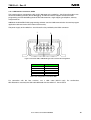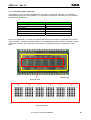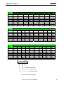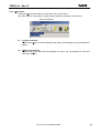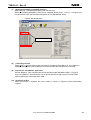
1
User’s Manual
78K0/Lx3 - See it!
Demonstration Kit for the
78K0 L_Series
Document No. U18759EE2V0UM00
Date Published July 2007
© NEC Electronics (Europe) GmbH
78K0/Lx3 - See it!
・ The information in this document is current as of date of its publication. The information is subject to
change without notice. For actual design-in, refer to the latest publications of NEC Electronics data
sheets or data books, etc., for the most up-to-date specifications of NEC Electronics products. Not all
products and/or types are available in every country. Please check with an NEC sales representative
for availability and additional information.
・ No part of this document may be copied or reproduced in any form or by any means without prior
written consent of NEC Electronics. NEC Electronics assumes no responsibility for any errors that may
appear in this document.
・ NEC Electronics does not assume any liability for infringement of patents, copyrights or other
intellectual property rights of third parties by or arising from the use of NEC Electronics products listed
in this document or any other liability arising from the use of such NEC Electronics products. No
license, express, implied or otherwise, is granted under any patents, copyrights or other intellectual
property rights of NEC Electronics or others.
・ Descriptions of circuits, software and other related information in this document are provided for
illustrative purposes in semiconductor product operation and application examples. The incorporation
of these circuits, software and information in the design of customer's equipment shall be done under
the full responsibility of customer. NEC Electronics no responsibility for any losses incurred by
customers or third parties arising from the use of these circuits, software and information.
・ While NEC Electronics endeavors to enhance the quality, reliability and safety of NEC Electronics
products, customers agree and acknowledge that the possibility of defects thereof cannot be
eliminated entirely. To minimize risks of damage to property or injury (including death) to persons
arising from defects in NEC Electronics products, customers must incorporate sufficient safety
measures in their design, such as redundancy, fire-containment and anti-failure features.
・ NEC Electronics products are classified into the following three quality grades: “Standard”, “Special”
and “Specific”.
The "Specific" quality grade applies only to NEC Electronics products developed based on a customerdesignated “quality assurance program” for a specific application. The recommended applications of NEC
Electronics product depend on its quality grade, as indicated below. Customers must check the quality
grade of each NEC Electronics product before using it in a particular application.
"Standard":
Computers, office equipment, communications equipment, test and measurement
equipment, audio and visual equipment, home electronic appliances, machine tools,
personal electronic equipment and industrial robots.
"Special":
Transportation equipment (automobiles, trains, ships, etc.), traffic control systems, antidisaster systems, anti-crime systems, safety equipment and medical equipment (not
specifically designed for life support).
"Specific":
Aircraft, aerospace equipment, submersible repeaters, nuclear reactor control systems,
life support systems and medical equipment for life support, etc.
The quality grade of NEC Electronics products is “Standard” unless otherwise expressly specified in NEC
Electronics data sheets or data books, etc. If customers wish to use NEC Electronics products in
applications not intended by NEC Electronics, they must contact NEC Electronics sales representative in
advance to determine NEC Electronics 's willingness to support a given application.
Notes: 1." NEC Electronics" as used in this statement means NEC Electronics Corporation and also
includes its majority-owned subsidiaries.
2. " NEC Electronics products" means any product developed or manufactured by or for NEC
Electronics (as defined above).
User’s Manual U18759EE2V0UM00
2
78K0/Lx3 - See it!
CAUTION
This is a Test- and Measurement equipment with possibility to be significantly
altered by user through hardware enhancements/modifications and/or test or
application software. Thus, with respect to Council Directive 89/336/EEC
(Directive on compliance with the EMC protection requirements), this equipment
has no autonomous function. Consequently this equipment is not marked by the
CE-symbol.
EEDT-ST-005-10
CAUTION
This equipment should be handled like a CMOS semiconductor device. The
user must take all precautions to avoid build-up of static electricity while
working with this equipment. All test and measurement tool including the
workbench must be grounded. The user/operator must be grounded using
the wrist strap. The connectors and/or device pins should not be touched
with bare hands.
EEDT-ST-004-10
Redemption of Waste Electrical and Electronic Equipment
(WEEE) in accordance with legal regulations applicable in the
European Union only: This equipment (including all
accessories) is not intended for household use. After use the
equipment cannot be disposed of as household waste. NEC
Electronics (Europe) GmbH offers to take back the equipment.
All you need to do is register at www.eu.necel.com/weee.
User’s Manual U18759EE2V0UM00
3
78K0/Lx3 - See it!
Regional Information
Some information contained in this document may vary from country to country. Before using any NEC
product in your application, please contact the NEC office in your country to obtain a list of authorized
representatives and distributors. They will verify:
•
•
•
•
•
•
Device availability
Ordering information
Product release schedule
Availability of related technical literature
Development environment specifications (for example, specifications for
third-party tools and components, host computers, power plugs, AC supply
voltages, and so forth)
Network requirements
In addition, trademarks, registered trademarks, export restrictions, and otherlegal issues may also vary
from country to country.
NEC Electronics Inc. (U.S.)
Santa Clara, California
Tel: 408-588-6000
800-366-9782
Fax: 408-588-6130
800-729-9288
NEC Electronics Hong Kong Ltd.
Hong Kong
Tel: 2886-9318
Fax: 2886-9022/9044
NEC Electronics (Europe) GmbH
Duesseldorf, Germany
Tel: 0211-65 03 0
Fax: 0211-65 03 1327
NEC Electronics Hong Kong Ltd.
Seoul Branch
Seoul, Korea
Tel: 02-528-0303
Fax: 02-528-4411
Sucursal en España
Madrid, Spain
Tel: 091- 504 27 87
Fax: 091- 504 28 60
NEC Electronics Singapore Pte. Ltd.
Singapore
Tel: 65-6253-8311
Fax: 65-6250-3583
Succursale Française
Vélizy-Villacoublay, France
Tel: 01-30-67 58 00
Fax: 01-30-67 58 99
NEC Electronics Taiwan Ltd.
Taipei, Taiwan
Tel: 02-2719-2377
Fax: 02-2719-5951
Filiale Italiana
Milano, Italy
Tel: 02-66 75 41
Fax: 02-66 75 42 99
NEC do Brasil S.A.
Electron Devices Division
Guarulhos, Brasil
Tel: 55-11-6465-6810
Fax: 55-11-6465-6829
Branch The Netherlands
Eindhoven, The Netherlands
Tel: 040-244 58 45
Fax: 040-244 45 80
Branch Sweden
Taeby, Sweden
Tel: 08-63 80 820
Fax: 08-63 80 388
United Kingdom Branch
Milton Keynes, UK
Tel: 01908-691-133
Fax: 01908-670-290
User’s Manual U18759EE2V0UM00
4
78K0/Lx3 - See it!
Revision History
Date
21-06-2007
20-07-2007
Revision
V1.00
V2.00
Chapter
--5, 7, 8, 9
Description
First release
Changed description from FPL3 to WriteEZ3 FLASH
programming software
User’s Manual U18759EE2V0UM00
5
78K0/Lx3 - See it!
Table of Contents
1.
Introduction ........................................................................................................................10
1.1
1.2
1.3
1.4
Main features of 78K0/Lx3 - See it!................................................................................................ 10
System requirements...................................................................................................................... 12
Package contents............................................................................................................................ 12
Trademarks ...................................................................................................................................... 12
2.
78K0/Lx3 - See it! system configuration..........................................................................13
2.1
2.2
2.3
78K0/Lx3 - See it! ............................................................................................................................ 13
Host computer ................................................................................................................................. 13
Power supply via USB interface .................................................................................................... 13
3.
78K0/Lx3 - See it! components.........................................................................................14
3.1
3.1.1
3.1.2
3.1.3
3.2
3.3
3.4
3.5
3.6
3.7
3.8
3.9
3.10
3.11
3.12
3.13
3.14
3.15
3.16
3.17
3.18
3.19
Configuration switches SW1 / SW2............................................................................................... 15
On-Board Debug Mode (TK-78 debugging)................................................................................... 15
FPL3(WriteEZ3) Mode (FLASH programming mode).................................................................... 15
QB-MINI2 Mode (OCD debugging / Normal execution mode) ...................................................... 15
RESET button, SW4 ........................................................................................................................ 16
Navigation switch, SW3.................................................................................................................. 16
External A/D measurement inputs, connector J1........................................................................ 17
External A/D measurement input, connector J2.......................................................................... 17
IDD measurement, connector J4 ................................................................................................... 17
External power supply input, connector J5 ................................................................................. 17
External main oscillator, Y1 ........................................................................................................... 17
QB-MINI2 connector, OCD1 ........................................................................................................... 18
USB interface connector, USB1 .................................................................................................. 19
LCD1, 224 segment LCD panel .................................................................................................... 20
External LCD resistors, RR1 – RR5............................................................................................. 22
Temperature sensor, U2 ............................................................................................................... 22
IR receiver module, U4 ................................................................................................................. 22
Buzzer, BUZ1 ................................................................................................................................. 22
Power LED, LED1 .......................................................................................................................... 22
Connectors T1 – T13 and wrap field ........................................................................................... 23
Soldering bridges.......................................................................................................................... 24
78K0/LF3 memory map................................................................................................................. 25
4.
On-Chip debugging ...........................................................................................................26
4.1
4.2
OCD via TK-78 debug function ...................................................................................................... 26
OCD via QB-MINI2 emulator........................................................................................................... 27
5.
78K0/Lx3 - See it! installation and operation ..................................................................28
5.1 Getting started................................................................................................................................. 28
5.1.1 CD-ROM contents.......................................................................................................................... 28
6.
Hardware installation.........................................................................................................29
7.
Software installation..........................................................................................................29
User’s Manual U18759EE2V0UM00
6
78K0/Lx3 - See it!
7.1
7.2
7.3
7.4
7.4.1
7.4.2
7.4.3
7.5
7.6
8.
IAR Systems Embedded Workbench for 78K installation .......................................................... 29
WriteEZ3 FLASH programming GUI installation.......................................................................... 29
Sample program installation.......................................................................................................... 29
USB Driver Installation ................................................................................................................... 30
Installation on Windows 98SE/Me ................................................................................................. 30
Installation on Windows 2000 ........................................................................................................ 32
Installation on Windows XP............................................................................................................ 38
Confirmation of USB Driver Installation ....................................................................................... 43
Driver deinstallation........................................................................................................................ 44
WriteEZ3 FLASH programming software ........................................................................46
8.1
8.2
8.3
8.4
8.4.1
8.4.2
8.4.3
8.4.4
8.5
Introduction ..................................................................................................................................... 46
Starting up the GUI Software ......................................................................................................... 46
Toolbar ............................................................................................................................................. 47
Menu Bar .......................................................................................................................................... 48
[File] menu...................................................................................................................................... 48
[Device] menu ................................................................................................................................ 49
[View] menu.................................................................................................................................... 58
[Help] menu .................................................................................................................................... 59
Programmer Parameter Window ................................................................................................... 60
9.
How to use WriteEZ3 FLASH programming software ....................................................61
(1)
(2)
(3)
(4)
(5)
(6)
(7)
(8)
(9)
(10)
Installing the WriteEZ3 GUI software ................................................................................................ 61
Installing the driver............................................................................................................................. 61
Installing the parameter file................................................................................................................ 61
Connecting and starting..................................................................................................................... 62
Setting the programming environment .............................................................................................. 63
Selecting a user program .................................................................................................................. 66
[Autoprocedure(EPV)] command execution ...................................................................................... 67
Terminating the GUI .......................................................................................................................... 67
Execute the “VOLTMETER” application ............................................................................................ 67
Restarting the GUI ........................................................................................................................... 67
10.
TROUBLESHOOTING ......................................................................................................68
11.
IAR sample session .........................................................................................................70
12.
Sample Projects ...............................................................................................................77
12.1
12.2
12.3
12.4
12.5
12.6
Buzzer sample ............................................................................................................................... 78
KitchenTimer sample.................................................................................................................... 78
RealTimeClock sample ................................................................................................................. 78
RemoteControl sample................................................................................................................. 78
Temperature sample ..................................................................................................................... 78
Voltmeter sample .......................................................................................................................... 78
13.
Cables ...............................................................................................................................79
13.1
USB interface cable (Mini-B type) ............................................................................................... 79
User’s Manual U18759EE2V0UM00
7
78K0/Lx3 - See it!
14.
Schematics .......................................................................................................................80
List of Figures
Figure 1: 78K0/Lx3 - See it! system configuration ......................................................................................13
Figure 2: 78K0/Lx3 - See it! board connectors and switches, top view ......................................................14
Figure 3: Connector USB1, USB Mini-B Type Host Connector Pin Configuration .....................................19
Figure 4: LCD outline...................................................................................................................................20
Figure 5: Connectors T1 – T13 and wrap field............................................................................................23
Figure 6: 78K0/LF3 memory map................................................................................................................25
Figure 7: On-Chip Debugging .....................................................................................................................26
Figure 8: Add New Hardware Wizard (Windows 98SE)..............................................................................30
Figure 9: Search Method (Windows 98SE).................................................................................................30
Figure 10: Search Location Specification (Windows 98SE)........................................................................31
Figure 11: Checking Driver to Be Installed (Windows 98SE)......................................................................31
Figure 12: Installation Completion (Windows 98SE)...................................................................................32
Figure 13: Found New Hardware Wizard 1 (Windows 2000)......................................................................32
Figure 14: Search Method 1 (Windows 2000).............................................................................................33
Figure 15: Driver File Location 1 (Windows 2000) ......................................................................................33
Figure 16: Address Specification 1 (Windows 2000) ..................................................................................34
Figure 17: Driver File Search 1 (Windows 2000) ........................................................................................34
Figure 18: USB Driver Installation Completion 1 (Windows 2000) .............................................................35
Figure 19: Found New Hardware Wizard 2 (Windows 2000)......................................................................35
Figure 20: Search Method 2 (Windows 2000).............................................................................................36
Figure 21: Driver File Location 2 (Windows 2000) ......................................................................................36
Figure 22: Address Specification 2 (Windows 2000) ..................................................................................37
Figure 23: Driver File Search 2 (Windows 2000) ........................................................................................37
Figure 24: USB Driver Installation Completion 2 (Windows 2000) .............................................................38
Figure 25: Found New Hardware Wizard 1 (Windows XP).........................................................................38
Figure 26: Search Location Specification 3 (Windows XP).........................................................................39
Figure 27: Windows XP Logo Testing 3 (Windows XP) ..............................................................................39
Figure 28: USB Driver Installation Completion 1 (Windows XP).................................................................40
Figure 29: Found New Hardware Wizard 2 (Windows XP).........................................................................40
Figure 30: Search Location Specification 2 (Windows XP).........................................................................41
Figure 31: Windows XP Logo Testing 2 (Windows XP) ..............................................................................41
Figure 32: USB Serial Port2 Driver Installation Completion (Windows XP)................................................42
Figure 33: Device Manager .........................................................................................................................43
Figure 34: Driver Uninstallation ...................................................................................................................44
Figure 35: Driver Uninstaller........................................................................................................................44
Figure 36: Completion of Driver Uninstallation............................................................................................45
Figure 37: GUI Software Main Window .......................................................................................................46
Figure 38: Toolbar Buttons ..........................................................................................................................47
Figure 39: [File] Menu..................................................................................................................................48
Figure 40: HEX File Selection Window .......................................................................................................48
Figure 41: [Device] Menu ............................................................................................................................49
Figure 42: Device Setup Window - Standard ..............................................................................................51
Figure 43: Device Setup Window - Parameter File Selection .....................................................................52
Figure 44: Parameter File Selection Window..............................................................................................52
Figure 45: Device Setup Window – Host connection ..................................................................................53
Figure 46: Device Setup Window - Supply Oscillator Selection..................................................................53
Figure 47: Device Setup Window - Operation Mode...................................................................................54
Figure 48: Device Setup Window – Target Reset Message .......................................................................54
Figure 49: Device Setup Window - Advance...............................................................................................55
Figure 50: Device Setup Window - Command options ...............................................................................55
Figure 51: Device Setup Window – Security flag settings ..........................................................................56
Figure 52: Device Setup Window – Disable Chip Erase.............................................................................57
Figure 53: Device Setup Window – Disable Boot Cluster Reprogramming warning ..................................57
User’s Manual U18759EE2V0UM00
8
78K0/Lx3 - See it!
Figure 54: [View] Menu................................................................................................................................58
Figure 55: [Help] Menu ................................................................................................................................59
Figure 56: About WriteEZ3 Window ............................................................................................................59
Figure 57: Programmer Parameter Window ...............................................................................................60
Figure 58: GUI Software Startup Screen.....................................................................................................63
Figure 59: <Standard Device Setup> Dialog Box .......................................................................................63
Figure 60: Parameter File Selection............................................................................................................64
Figure 61: Port Selection .............................................................................................................................64
Figure 62: <Standard Device Setup> Dialog Box after Setting...................................................................65
Figure 63: <Advance Device Setup> Dialog Box ........................................................................................65
Figure 64: Completion of Parameter Setting ...............................................................................................66
Figure 65: After Downloading......................................................................................................................66
Figure 66: After EPV Execution...................................................................................................................67
Figure 67: IAR Embedded Workbench .......................................................................................................71
Figure 68: IAR project workspace ...............................................................................................................72
Figure 69: IAR debugger options 1/2 ..........................................................................................................72
Figure 70: IAR debugger options 2/2 ..........................................................................................................73
Figure 71: IAR Linker options......................................................................................................................73
Figure 72: TK-78 hardware setup menu .....................................................................................................74
Figure 73: IAR project download .................................................................................................................75
Figure 74: IAR C-SPY debugger .................................................................................................................76
Figure 75: USB interface cable (Mini-B type)..............................................................................................79
Figure 76: 78K0/Lx3 - See it! schematics 1/2 .............................................................................................80
Figure 77: 78K0/Lx3 - See it! schematics 2/2 .............................................................................................81
List of Tables
Table 1: Operation mode selection SW1 / SW2..........................................................................................15
Table 2: Navigation switch SW3..................................................................................................................16
Table 3: External A/D measurement inputs, connector J1..........................................................................17
Table 4: External A/D measurement input, connector J2 ...........................................................................17
Table 5: External power supply input, J3 ....................................................................................................17
Table 6: QB-MINI2 connector OCD1...........................................................................................................18
Table 7: Configuration of SW1 and SW2 when using QB-MINI2................................................................18
Table 8: Pin Configuration of Connector USB1...........................................................................................19
Table 9: LCD driver specification ................................................................................................................20
Table 10: LCD segment assignment ...........................................................................................................21
Table 11: Connectors T1 – T13...................................................................................................................23
Table 12: Setting of soldering bridges A1 – A8, V7 ....................................................................................24
Table 13: Setting of soldering bridges V1 – V6, V8 – V11 ..........................................................................24
Table 14: Configuration for TK-78 debugging .............................................................................................26
Table 15: Configuration for QB-MINI2 debugging.......................................................................................27
Table 16: 78K0/Lx3 - See it! CD-ROM directory structure..........................................................................28
Table 17: Example directory structure ........................................................................................................77
User’s Manual U18759EE2V0UM00
9
78K0/Lx3 - See it!
1. Introduction
78K0/Lx3 - See it! is a demonstration kit for the 78K0 L_Series 8-bit microcontrollers with integrated LCD
controller. It supports On-Board debugging, FLASH programming and real time execution of application
programs based on the 78K0/LF3 microcontroller. The board is prepared to be connected to user
hardware parts such as digital I/O or analogue signals.
1.1 Main features of 78K0/Lx3 - See it!
•
Easy to use device demonstration capabilities
78K0/Lx3 - See it! contains elements to easily demonstrate simple I/O-functions, i.e. navigator switch,
224 segment LCD panel, temperature sensor, IR receiver module, I/O lines, UART serial interface
etc.
•
TK-78 debugging
The 78K0/Lx3 – See it! supports an On-Board debug function by using the IAR C-SPY debugger and
the UART / USB interface without a need of additional debug hardware. It allows FLASH
programming and supports standard debug functions i.e. code execution, single stepping, software
breakpoints, memory manipulation etc.
•
OCD debugging
The 78K0/Lx3 – See it! is prepared to be equipped with a 10-pin connector in order to connect the
QB-MINI2 On-Chip debug emulator to use the On-Chip debug function of the 78K0/LF3 device.
Please note, the QB-MINI2 is separate product from NEC and it is not included in this starterkit
package.
•
Flexible power supply
The 78K0/Lx3 - See it! supports a flexible configuration of it’s power supply. The board can be
powered by the USB interface, the QB-MINI2 On-Chip debug emulator as well by an external power
supply.
•
LCD panel
78K0/Lx3 - See it! provides a 224 segment LCD panel, allowing the implementation of
human / machine interface, comfortable input / output functions, output of measurement values,
output of status information etc.
•
WriteEZ3, FLASH programming software
A windows based FLASH programming software allows to select and download application programs
to the 78K0/Lx3 - See it! board for evaluation purposes.
•
Various input / output signals available, such as
°
°
°
°
°
°
°
°
°
°
I/O ports prepared to be connected to user hardware
224 segment LCD panel
Timer input / output signals
Two or three wire serial I/O
UART interface, via USB UART chip FT232
Eight channel 10-bit A/D converter
Three channel 16-bit ∆∑ A/D converter
IR receiver module RPM7138
Temperature sensor S-8120C
Navigation switch prepared for key interrupt generation
•
The IAR Embedded Workbench for 78K and the IAR C-SPY debugger / simulator are included. This
package is restricted in such that maximum program code size is limited to 4 kByte of program code.
•
Full documentation is included for the 78K0/LF3 microcontroller, IAR Systems Embedded
Workbench, IAR Systems C-SPY debugger / simulator and the WriteEZ3 FLASH programming
software
User’s Manual U18759EE2V0UM00
10
78K0/Lx3 - See it!
CAUTION
The 78K0/Lx3 - See it! starterkit is not intended for code development. NEC does
not allow and does not support in any way any attempt to use 78K0/Lx3 - See it!
in a commercial or technical product.
User’s Manual U18759EE2V0UM00
11
78K0/Lx3 - See it!
1.2 System requirements
HOST PC
A PC supporting Windows 98SE, Windows ME, Windows 2000 or
Windows XP is required for the IAR Systems Embedded Workbench
demo-version and the WriteEZ3 FLASH programming software.
Pentium 166 MHz (at least), 128 MB of RAM, 256-color display (1024 *
768), mouse, CD-ROM drive and 200 Mbytes of free hard disk space are
required to install the tool packages.
Above listed requirements are valid for the IAR Systems Embedded
Workbench and the WriteEZ3 FLASH programming software.
Host interface
USB interface that enables communication based on USB (Ver1.1 or
later)
1.3 Package contents
Please verify that you have received all parts listed in the package contents list attached to the
78K0/Lx3 - See it! package. If any part is missing or seems to be damaged, please contact the dealer
from whom you received your 78K0/Lx3 - See it!.
Note:
Updates of the IAR Embedded Workbench for 78K, FP3 FLASH programming software,
documentation and/or utilities for 78K0/Lx3 - See it!, if available, may be downloaded from the
NEC WEB page(s) at http://www.eu.necel.com/updates
1.4 Trademarks
IAR Embedded Workbench, visualSTATE, IAR MakeApp and C-SPY are registered trademarks of IAR
Systems AB. Microsoft and Windows are registered trademarks of Microsoft Corporation. Adobe and
Acrobat Reader are registered trademarks of Adobe Systems Incorporated.
All other product names are trademarks or registered trademarks of their respective owners.
User’s Manual U18759EE2V0UM00
12
78K0/Lx3 - See it!
2. 78K0/Lx3 - See it! system configuration
The 78K0/Lx3 - See it! system configuration is given in the diagram below:
Figure 1: 78K0/Lx3 - See it! system configuration
2.1 78K0/Lx3 - See it!
78K0/Lx3 - See it! is a demonstration kit for the 78K0/LF3 8-Bit microcontroller with integrated LCD
controller. The 78K0/Lx3 - See it! board is connected to the host system via USB interface cable. The
host system may be used for onboard FLASH programming of the 78K0/LF3 internal FLASH memory
and to allow execution of application programs on 78K0/Lx3 - See it! starterkit. Additionally it supports
On-Chip debug functionality by using the IAR C-SPY debugger.
78K0/Lx3 - See it! runs the microcontroller at 8.0000 MHz operating speed. Per default the internal highspeed oscillator of the 78K0/LF3 device is used. The Sub-clock is provided with 32.768 kHz.
2.2 Host computer
The USB host interface enables communication to the 78K0/Lx3 - See it! board. The USB UART chip
FT232 allows application software to access the USB device in the same way as it would access a
standard RS232 interface. The FTDI's Virtual COM Port ( VCP ) driver appears to the windows system as
an extra Com Port, in addition to any existing hardware Com Ports.
2.3 Power supply via USB interface
The 78K0/Lx3 - See it! supports a flexible configuration of it’s power supply. The board can be powered
by the USB interface, the QB-MINI2 On-Chip debug emulator as well by an external power supply.
User’s Manual U18759EE2V0UM00
13
78K0/Lx3 - See it!
3. 78K0/Lx3 - See it! components
The 78K0/Lx3 - See it! board is equipped with a navigation switch, a 224 segment LCD panel,
temperature sensor and with several connectors in order to be connected to host computers, FLASH
programmer or any external target hardware.
Figure 2: 78K0/Lx3 - See it! board connectors and switches, top view
Some of the 78K0/Lx3 - See it! components are free for user application hardware and software. Please
read the user’s manual of the 78K0/LF3 device carefully to get information about the electrical
specification of the available I/O ports before you connect any external signals to the 78K0/Lx3 - See it!
board.
User’s Manual U18759EE2V0UM00
14
78K0/Lx3 - See it!
3.1 Configuration switches SW1 / SW2
The different operation modes of the 78K0/Lx3 - See it! board can be set by switches SW1 and SW2.
SW2
SW1
Mode
On-Board
Debug
1
2
ON
ON
FPL3
(WriteEZ3)
OFF
OFF
QB-MINI2
ON
ON
3
4
OFF
OFF
ON
ON
5
6
7
8
1
2
3
4
5
6
ON
ON
ON
ON
ON
ON
don’t care
ON
ON
don’t care
OFF
OFF
don’t care
OFF
OFF
OFF
OFF
OFF
OFF
OFF
OFF
OFF
OFF
7
8
OFF
OFF
ON
ON
OFF
OFF
Table 1: Operation mode selection SW1 / SW2
3.1.1 On-Board Debug Mode (TK-78 debugging)
Within this mode On-Board debugging is enabled. By using this mode no additional debug hardware like
the QB-MINI2 On-Chip debug emulator is needed. The debugging is done via the default USB/UART
connection to the Host computer. All standard debug function are available in the On-Board debug mode
like FLASH programming / downloading, code execution, single stepping, breakpoints, memory
manipulation etc.
3.1.2 FPL3(WriteEZ3) Mode (FLASH programming mode)
This mode allows to reprogram the internal FLASH memory of the 78K0/LF3 device by using the
WriteEZ3 FLASH programming software. Within this mode FLASH programming is done by using the
default USB/UART connection to the Host computer.
3.1.3 QB-MINI2 Mode (OCD debugging / Normal execution mode)
Within this mode the QB-MINI2 On-Chip debug emulator can be connected to the 78K0/Lx3 - See it!
board in order to use On-Chip debug function of the 78K0/LF3 device.
Additional, when no QB-MINI2 On-Chip debug emulator is connected to the 78K0/Lx3 - See it! board the
78K0/LF3 device starts within normal execution mode and the user program stored in the FLASH
memory is executed.
User’s Manual U18759EE2V0UM00
15
78K0/Lx3 - See it!
3.2 RESET button, SW4
SW4 is the reset button. It activates the power on reset. It is connected to the reset input of the 78K0/LF3
microcontroller.
3.3 Navigation switch, SW3
Button SW3 is a navigation switch connected to the key interrupt port of the 78K0/LF3 device. It operates
in five directions including a center push function. The connection of SW3 is shown in the table below:
SW3
Connection to the
78K0/LF3 device
Left
Down
Push
Right
Up
P43/KR3
P42/KR2
P44/KR4
P45/KR5
P46/KR6
Table 2: Navigation switch SW3
User’s Manual U18759EE2V0UM00
16
78K0/Lx3 - See it!
3.4 External A/D measurement inputs, connector J1
Connector J1 can be configured to measure external analogue signals by using the internal 10-Bit A/D
converter or respectively the 16-bit ∆∑ A/D converter of the 78K0/LF3 device. To use this mode please
open the corresponding soldering bridges A1 - A8.
J1
1
2
3
4
5
6
7
8
Signal
P20/ANI0/DS0P21/ANI1/DS0+
P22/ANI2/DS1P23/ANI3/DS1+
P24/ANI4/DS2P25/ANI5/DS2+
P26/ANI6/REFP27/ANI7/REF+
J1
9
10
11
12
13
14
15
16
Signal
GND
GND
GND
GND
GND
GND
GND
GND
Table 3: External A/D measurement inputs, connector J1
3.5 External A/D measurement input, connector J2
Connector J2 can be used to measure an external analogue signal by using the internal 10-Bit A/D
converter or respectively the 16-bit ∆∑ A/D converter of the 78K0/LF3 device.
J2
1
2
Signal
P23/ANI3/DS1+
GND
Table 4: External A/D measurement input, connector J2
3.6 IDD measurement, connector J4
Connector J4 (not assembled) can be used to measure the current consumption of the 78K0/LF3 device.
For using this mode please open soldering bridge V8.
3.7 External power supply input, connector J5
By using connector J5 (not assembled) external power supply can be applied to the 78K0/Lx3 - See it!
board without a need of an active USB connection.
J5
1
2
Input
VDD (+5V)
GND
Table 5: External power supply input, J3
Note:
Be sure to unplug the USB connection before applying external power supply to input J5.
3.8 External main oscillator, Y1
The clock generator of the 78K0/LF3 device can be configured to work with an external oscillator
connected to the X1 and X2 pins. To use this mode equip pad Y1 of the 78K0/Lx3 - See it! board with an
corresponding oscillator. The configuration of the clock generator is described within the user’s manual of
the 78K0/LF3 device.
User’s Manual U18759EE2V0UM00
17
78K0/Lx3 - See it!
3.9 QB-MINI2 connector, OCD1
Connector OCD1 (not assembled) allows connecting the QB-MINI2 On-Chip debug emulator to the
78K0/Lx3 - See it! board in order to use On-Chip debug function of the 78K0/LF3 device. Please note,
QB-MINI2 is a separate product from NEC and it is not included in this starterkit package.
OCD1
1
2
3
4
5
6
7
8
9
10
Signal
RESET_IN
RESET_OUT
FLMDO
VDD_IN
X2
GND
X1
GND
not connected
VDD
Table 6: QB-MINI2 connector OCD1
When using QB-MINI2 for debugging purpose, please configure switch SW2 of the 78K0/Lx3 - See it!
board as following:
SW2
SW1
Mode
QB-MINI2
1
2
ON
ON
3
4
OFF
OFF
5
6
7
don’t care
8
1
2
3
4
5
6
7
8
OFF
OFF
OFF
OFF
OFF
OFF
OFF
OFF
Table 7: Configuration of SW1 and SW2 when using QB-MINI2
For more details on how to configure 78K0/Lx3 - See it! in order to use On-Chip debugging please refer
to CHAPTER 4, ON-CHIP DEBUGGING.
User’s Manual U18759EE2V0UM00
18
78K0/Lx3 - See it!
3.10 USB interface connector, USB1
This interface allows connecting the IAR C-SPY debugger to the 78K0/Lx3 - See it! board in order to use
the On-Board debug function (TK-78 debugging). The TK-78 interface supports On-board FLASH
programming and standard debug features like code execution, single stepping, breakpoints, memory
manipulation etc.
Additional the WriteEZ3 FLASH programming software uses the USB communication channel to program
application software into the CPU internal flash memory.
The power supply of the 78K0/Lx3 - See it! board is also provided by the USB1 connector.
1
5
Figure 3: Connector USB1, USB Mini-B Type Host Connector Pin Configuration
Connector USB1
1
2
3
4
5
Signal Name
VBUS
DD+
not connected
GND
Table 8: Pin Configuration of Connector USB1
For connection with the host machine, use a USB cable (Mini-B type). For confirmation,
NEC Electronics used only the USB cable delivered with the 78K0/Lx3 - See it! board.
User’s Manual U18759EE2V0UM00
19
78K0/Lx3 - See it!
3.11 LCD1, 224 segment LCD panel
The 78K0/Lx3 - See it! board is equipped with a 224 segment LCD panel. The LCD is a transflective
model type operating at 5V supply voltage. It can operate at a eight times multiplex rate. The LCD driver
specification is as following:
LCD driver specification
Driver voltage generation
Bias method
Timesharing
Common signals
Segment number
Number of maximum display pixels
Mode
Internal resistance division
1/4
8
8 (COM0-COM7)
28 (SEG4-SEG31)
224 (28 segments × 8 common)
Table 9: LCD driver specification
The LCD is divided into a character and indicator field. The character field is composed of six 5x7 DOT
matrix characters. The indicator field includes a set of predefined symbols, for instance weekday, battery
and antenna symbols. The outline of the LCD and the corresponding segment assignment is shown
below.
Indicator field
Character field
Figure 4: LCD outline
User’s Manual U18759EE2V0UM00
20
78K0/Lx3 - See it!
Bit
position
bit7
bit6
bit5
bit4
bit3
bit2
bit1
bit0
Bit
position
bit7
bit6
bit5
bit4
bit3
bit2
bit1
bit0
Bit
positio
n
bit7
bit6
bit5
bit4
bit3
bit2
bit1
bit0
+27
+26
+25
LCD RAM address
+24
+23
ALARM
AM
PM
Sun
520
510
500
521
511
522
512
523
+22
+21
+20
SUN
(symbol)
420
Mon
440
MOON
(symbol)
430
410
All FLASH
78K0/Lx3
400
501
441
431
421
411
401
502
442
432
422
412
402
513
503
443
433
423
413
403
524
514
504
444
434
424
414
404
525
515
505
445
435
425
415
405
526
516
506
446
436
426
416
406
LCD RAM address
+15
+14
+13
+19
+18
+17
+16
+12
+11
Tue
Wed
Thur
Fri
Sat
V
A
mA
Hz
Rem
340
330
320
310
300
000
010
020
030
040
341
331
321
311
301
001
011
021
031
041
342
332
322
312
302
002
012
022
032
042
343
333
323
313
303
003
013
023
033
043
344
334
324
314
304
004
014
024
034
044
345
335
325
315
305
005
015
025
035
045
346
336
326
316
306
006
016
026
036
046
+9
+8
+7
+6
Bt3
(Battery)
100
Bt2
Bt1
BtM
110
120
101
111
121
102
112
103
113
104
LCD RAM address
+5
+4
+3
+10
+2
+1
+0
An4
An3
An2
An1
AnM
130
An5
(Antenna)
140
200
210
220
230
240
131
141
201
211
221
231
241
122
132
142
202
212
222
232
242
123
133
143
203
213
223
233
243
114
124
134
144
204
214
224
234
244
105
115
125
135
145
205
215
225
235
245
106
116
126
136
146
206
216
226
236
246
1
3
6
Row index
Colomn index
Character index
Table 10: LCD segment assignment
User’s Manual U18759EE2V0UM00
21
78K0/Lx3 - See it!
3.12 External LCD resistors, RR1 – RR5
The 78K0/Lx3 - See it! board can also be configured to use external voltage divider resistors for the
generation of the LCD drive power supplies. For more details on the external resistance division method
please refer to the user’s manual of the 78K0/LF3 device.
3.13 Temperature sensor, U2
For temperature measurement and primarily as an application example the 78K0/Lx3 - See it! board is
equipped within an temperature sensor IC (type S-8120C). The output pin of the temperature sensor is
connected to pin P21/ANI1/DS0+ of the 78K0/LF3 device.
3.14 IR receiver module, U4
For remote control application an IR receiver module is equipped on the 78K0/Lx3 - See it! board. The
output terminal of the IR receiver (type RPM7138) is connected to the remote control input pin
P41/KR1/RIN of the 78K0/LF3 device.
3.15 Buzzer, BUZ1
To generate acoustic signals and sound waves a buzzer is connected to the timer output port of the 16Bit Timer/Event Counter 00, equal to port P34/TI52/TI010/TO00/RTC1HZ/INTP1 of the 78K0/LF3 device.
The AC buzzer operates in a voltage range of 2V…5V.
3.16 Power LED, LED1
LED1 is the power LED of the 78K0/Lx3 – See it! board. It indicates if power is applied to the 78K0/Lx3 –
See it! board.
User’s Manual U18759EE2V0UM00
22
78K0/Lx3 - See it!
3.17 Connectors T1 – T13 and wrap field
Several pins of the 78K0/LF3 microcontroller are combined to the connectors T1 – T13. The
corresponding assignment can be found in table below. Additional the 78K0/Lx3 - See it! board provides
a wire wrap field area allowing the integration of additional application hardware.
wrap
field
connectors
T1 – T13
Figure 5: Connectors T1 – T13 and wrap field
Connector
T1
T2
T3
T4
T5
T6
T7
T8
T9
T10
T11
T12
T13
78K0/LF3
I/O pin
P14 / SCKA0 / INTP4
P32 / TOH0 / MCG0
P13 / SO10 / TxD0
P33 / TIO00 / RTCDIV / RTCCL / BUZ / INTP2
P12 / SI10 / RxD0
P16 / SOA0 / TxD6
P30 / INTP5
P11 / SCK10
P15 / SIA0 / RxD6
P31 / TOH1 / INTP3
P10 / PCL
P120 / INTP0 / EXLVI
P47 / KR7
Table 11: Connectors T1 – T13
User’s Manual U18759EE2V0UM00
23
78K0/Lx3 - See it!
3.18 Soldering bridges
Additional configuration of the 78K0/Lx3 - See it! board can be done by the soldering bridges A1 – A8 and
V1 – V11. The different configuration modes are shown in the tables below.
The soldering bridges A1 – A8 and V7 can be used to reconfigure the A/D converter input channels and
the reference input voltage.
Soldering
bridge
A1
A2
A3
A4
A5
A6
A7
A8
V7
Configuration
Closed (default)
Open
Closed (default)
Open
Closed (default)
Open
Closed (default)
Open
Closed (default)
Open
Closed (default)
Open
Closed (default)
Open
Closed (default)
Open
Closed (default)
Open
78K0/LF3 pin
ANI0/DS0ANI1/DS0+
ANI2/DS1ANI3/DS1+
ANI4/DS2ANI5/DS2+
ANI6/REFANI7/REF+
AVREF
connected to VSS
disconnected from VSS
connected to temperature sensor U2
disconnected from to temperature sensor U2
connected to VSS
disconnected from VSS
pin connected to jumper J2
disconnected from jumper J2
connected to VSS
disconnected from VSS
connected to VDD27
disconnected from VDD27
connected to VSS
disconnected from VSS
connected to VDD
disconnected from VDD
connected to VDD
disconnected from VDD
Table 12: Setting of soldering bridges A1 – A8, V7
The soldering bridges V1 – V6 and V8 - V11 can be used to reconfigure the power supply of dedicated
circuits of the 78K0/Lx3 - See it! board. For more details please refer also to the schematics of the
78K0/Lx3 - See it! board.
Soldering
bridge
V1
V2
V3
V6
V8
V9
V10
V11
Configuration
Closed (default)
Open
Closed (default)
Open
Closed (default)
Open
Closed (default)
Open
Closed (default)
Open
Closed (default)
Open
Closed (default)
Open
Closed (default)
Open
Circuit
BUZ1
U6 (not assembled)
U2
U5
U1
LED1
connected to VDD
disconnected from VDD
connected to VDD
disconnected from VDD
connected to VDD27
disconnected from VDD27
connected to VDD
disconnected from VDD
connected to VDD
disconnected from VDD
connected to VDD
disconnected from VDD
VDD connected to USBVDD
VDD disconnected from USBVDD
VDD2 connected to VDD
VDD2 disconnected from VDD
Table 13: Setting of soldering bridges V1 – V6, V8 – V11
User’s Manual U18759EE2V0UM00
24
78K0/Lx3 - See it!
3.19 78K0/LF3 memory map
The memory layout of 78K0/LF3 device shown in the figure below.
Figure 6: 78K0/LF3 memory map
The 78K0/Lx3 - See it! does not reserve any resources of the 78K0/LF3 device, consequently all
available memory of the device is free for application software.
User’s Manual U18759EE2V0UM00
25
78K0/Lx3 - See it!
4. On-Chip debugging
The 78K0/Lx3 - See it! board offers two possibilities to use On-Chip debugging. The TK-78 debug
function of 78K0/Lx3 - See it! allows On-Chip debugging without a need of external debug hardware.
Within this mode the default USB / UART connection to the Host computer is used as debug interface. All
standard debug functions are available in the On-Board debugging mode like FLASH programming /
downloading, code execution, single stepping, breakpoints, memory manipulation etc.
Additionally 78K0/Lx3 - See it! supports the QB-MINI2 On-Chip debug emulator in order to use On-Chip
debug function of the 78K0/LF3 device. The system configuration for On-Chip debugging is shown in
figure below.
Figure 7: On-Chip Debugging
4.1 OCD via TK-78 debug function
To operate the 78K0/Lx3 - See it! board within the On-Board debug mode, configure switches SW1 and
SW2 as following:
SW2
SW1
Mode
On-Board
Debug
1
2
ON
ON
3
OFF
4
OFF
5
6
7
8
1
2
3
4
5
6
ON
ON
ON
ON
ON
ON
don’t care
7
8
OFF
OFF
Table 14: Configuration for TK-78 debugging
User’s Manual U18759EE2V0UM00
26
78K0/Lx3 - See it!
4.2 OCD via QB-MINI2 emulator
To operate the 78K0/Lx3 - See it! board together with the QB-MINI2 On-Chip debug emulator, configure
switches SW1 and SW2 as following:
SW2
SW1
Mode
QB-MINI2
1
2
ON
ON
3
4
OFF
OFF
5
6
7
don’t care
8
1
2
3
4
5
6
7
8
OFF
OFF
OFF
OFF
OFF
OFF
OFF
OFF
Table 15: Configuration for QB-MINI2 debugging
Note:
By supplying power from the QB-MINI2 do not connect external hardware to the
78K0/Lx3 - See it! board. Within this mode the 78K0/Lx3 - See it! board can operate without
external power supply from USB.
User’s Manual U18759EE2V0UM00
27
78K0/Lx3 - See it!
5. 78K0/Lx3 - See it! installation and operation
5.1 Getting started
The IAR C-SPY debugger allows to download and debug application software on the 78K0/Lx3 - See it!
starterkit hardware. Additionally the WriteEZ3 FLASH programming software can be used for simple
FLASH programming of the 78K0/LF3 internal FLASH memory. As communication interface between the
host computer and the 78K0/Lx3 - See it! board a USB interface line is needed. Before you can
download, debug or execute an application program, hardware and software must be installed properly.
5.1.1 CD-ROM contents
The CD-ROM shows following directory structure:
CD-ROM ROOT
- Acrobat Reader for 32Bit Windows OS
78K0/Lx3 - See it! (F:)
Acrobat
Doc
- Documentation
WriteEZ3
- WriteEZ3 FLASH programming software
Drivers
… USB driver
WriteEZ3
… WriteEZ3 setup directory
PRM
… PRM parameter files
IAR Embedded Workbench 78K
- IAR Embedded Workbench for 78K
SamplePrograms
- Sample programs for 78K0/Lx3 - See it!
Table 16: 78K0/Lx3 - See it! CD-ROM directory structure
User’s Manual U18759EE2V0UM00
28
78K0/Lx3 - See it!
6. Hardware installation
After unpacking 78K0/Lx3 - See it!, connect the board to your host computer using the provided USB
interface cable. When 78K0/Lx3 - See it! is connected, the USB driver needs to be installed on the host
machine. Please refer to the following CHAPTER 7 SOFTWARE INSTALLATION.
7. Software installation
The 78K0/Lx3 - See it! package comes with several software demo packages:
•
•
•
IAR Systems Embedded Workbench for 78K, including C compiler, assembler, linker, librarian and IAR
C-SPY debugger / simulator
WriteEZ3 FLASH programming software
Sample program
The IAR Systems Embedded Workbench and the WriteEZ3 FLASH programming GUI must be installed on
your PC. For detailed installation hints, refer to the following chapters and to the corresponding
documentation of the IAR Embedded Workbench.
7.1 IAR Systems Embedded Workbench for 78K installation
To install the IAR Systems Embedded Workbench for 78K including C-SPY debugger / simulator, select the
SETUP program in the directory \IAR Embedded Workbench 78K\ew78k\ of the CDROM. The setup
dialogues will guide you through the installation process.
7.2 WriteEZ3 FLASH programming GUI installation
To install the WriteEZ3 FLASH programming GUI select the SETUP program in the directory \WriteEZ3\ of
the CDROM. The setup dialogues will guide you through the installation process.
7.3 Sample program installation
To install the sample/demonstration program for the 78K0/Lx3 - See it! board select the SETUP program in
the directory \SamplePrograms\ of the CDROM. The setup dialogues will guide you through the
installation process.
User’s Manual U18759EE2V0UM00
29
78K0/Lx3 - See it!
7.4 USB Driver Installation
In order to use the 78K0/Lx3 - See it! board for On-Chip debugging or FLASH programming,
the USB driver needs to be installed on the host machine. Install the driver according to the
following procedure:
Installation on Windows 98SE/Me ......... Page 30
Installation on Windows 2000 ................ Page 32
Installation on Windows XP ................... Page 38
7.4.1 Installation on Windows 98SE/Me
1.
When the 78K0/Lx3 - See it! board is connected with the host machine, the board is
recognized by Plug and Play, and the wizard for adding new hardware is started. Click
Next>.
Figure 8: Add New Hardware Wizard (Windows 98SE)
Click.
2.
The window below is displayed. So, check that "Search for a suitable driver ..." is selected,
then click Next>.
Figure 9: Search Method (Windows 98SE)
Check that "Search for a
suitable driver ..." is selected.
Click.
User’s Manual U18759EE2V0UM00
30
78K0/Lx3 - See it!
3.
Check the "Specify a location" check box only and enter "C:\Program Files\NECTools32\
WriteEZ3\DRIVER" in the address bar, then click Next>.
Figure 10: Search Location Specification (Windows 98SE)
<1> Check "Specify
a location" only.
<3> Click.
<2> Enter "C:\Program Files\NECTools32\WriteEZ3\DRIVER".
備考 3.1ソフトウエアのインストール先のフォルダを変更した場合は,
Remark
4.
If the installation destination folder is changed at the time of GUI software installation,
enter "new-folder\DRIVER".
The window below is displayed. Click Next>.
Figure 11: Checking Driver to Be Installed (Windows 98SE)
Click.
User’s Manual U18759EE2V0UM00
31
78K0/Lx3 - See it!
5.
When the window below is displayed, the installation of the USB driver is completed. Click
Finish. The installation of the USB Serial Port driver is then automatically performed.
Figure 12: Installation Completion (Windows 98SE)
Click.
7.4.2 Installation on Windows 2000
1.
When the 78K0/Lx3 - See it! board is connected with the host machine, the board is
recognized by Plug and Play, and the wizard for finding new hardware is started. Click
Next>.
Figure 13: Found New Hardware Wizard 1 (Windows 2000)
Click.
User’s Manual U18759EE2V0UM00
32
78K0/Lx3 - See it!
2.
The window below is displayed. So, check that "Search for a suitable driver ..." is selected,
then click Next>.
Figure 14: Search Method 1 (Windows 2000)
Check that "Search for a
suitable driver ..." is selected.
Click.
3.
Check the "Specify a location" check box only, then click Next>.
Figure 15: Driver File Location 1 (Windows 2000)
Check that "Specify a
location" only is checked.
ed.hed.
Click.
User’s Manual U18759EE2V0UM00
33
78K0/Lx3 - See it!
4.
Enter "C:\Program Files\NECTools32\WriteEZ3\DRIVER" in the address bar, then click OK.
Figure 16: Address Specification 1 (Windows 2000)
Click.
Enter "C:\Program Files\NECTools32\WriteEZ3\DRIVER".
Remark
5.
If the installation destination folder is changed at the time of GUI software installation,
enter "new-folder\WriteEZ3\DRIVER".
Click Next>.
Figure 17: Driver File Search 1 (Windows 2000)
Click.
User’s Manual U18759EE2V0UM00
34
78K0/Lx3 - See it!
6.
Click Finish to complete the installation of the USB driver.
Figure 18: USB Driver Installation Completion 1 (Windows 2000)
Click.
7.
Proceed to the installation of the USB Serial Port driver. Click Next>.
Figure 19: Found New Hardware Wizard 2 (Windows 2000)
Click.
User’s Manual U18759EE2V0UM00
35
78K0/Lx3 - See it!
8.
The window below is displayed. So, check that "Search for a suitable driver ..." is selected,
then click Next>.
Figure 20: Search Method 2 (Windows 2000)
Check that "Search for a
suitable driver ..." is selected.
Click.
9.
Check the "Specify a location" check box only, then click Next>.
Figure 21: Driver File Location 2 (Windows 2000)
Check that "Specify a
location" only is checked.
Click.
User’s Manual U18759EE2V0UM00
36
78K0/Lx3 - See it!
10. Enter "C:\Program Files\NECTools32\WriteEZ3\DRIVER" in the address bar, then click OK.
Figure 22: Address Specification 2 (Windows 2000)
Click.
Enter "C:\Program Files\NECTools32\WriteEZ3\DRIVER".
Remark
If the installation destination folder is changed at the time of GUI software installation,
enter "new-folder\DRIVER".
11. Click Next>.
Figure 23: Driver File Search 2 (Windows 2000)
Click.
User’s Manual U18759EE2V0UM00
37
78K0/Lx3 - See it!
12. Click Finish to complete the installation of the USB driver.
Figure 24: USB Driver Installation Completion 2 (Windows 2000)
Click.
7.4.3 Installation on Windows XP
1.
When the 78K0/Lx3 - See it! board is connected with the host machine, the board is
recognized by Plug and Play, and the wizard for finding new hardware is started. Check
that "Install from a list or specific ..." is selected, then click Next>.
Figure 25: Found New Hardware Wizard 1 (Windows XP)
Check that "Install from a list or
specific ..." is selected.
User’s Manual U18759EE2V0UM00
Click.
38
78K0/Lx3 - See it!
2.
Check that "Search for the best driver in these locations." is selected. Check the "Include
this
location
in
the
search:"
check
box
and
enter
"C:\Program
Files\NECTools32\WriteEZ3\DRIVER" in the address bar, then click Next>.
Figure 26: Search Location Specification 3 (Windows XP)
<1> Check that "Search for the
best driver in these locations."
is selected.
<2> Check "Include this
location in the search:"
only.
<3> Enter "C:\Program Files\NECTools32\WriteEZ3\DRIVER".
3.
<4> Click.
As shown below, "has not passed Windows Logo testing to verify its compatibility with
Windows XP." is displayed. Click Continue Anyway.
Figure 27: Windows XP Logo Testing 3 (Windows XP)
Click.
User’s Manual U18759EE2V0UM00
39
78K0/Lx3 - See it!
4.
When the window below is displayed, the installation of the USB driver is completed. Click
Finish.
Figure 28: USB Driver Installation Completion 1 (Windows XP)
Click.
5.
Proceed to the installation of the USB Serial Port driver. Click Next>.
Figure 29: Found New Hardware Wizard 2 (Windows XP)
Check that "Install from a list
or specific ..." is selected.
User’s Manual U18759EE2V0UM00
Click.
40
78K0/Lx3 - See it!
6.
Check that "Search for the best driver in these locations." is selected. Check the "Include
this
location
in
the
search:"
check
box
and
enter
"C:\Program
Files\NECTools32\WriteEZ3\DRIVER", then click Next>.
Figure 30: Search Location Specification 2 (Windows XP)
<1> Check that "Search for the best
driver in these locations." is
selected.
<2> Check "Include this location in
the search:" only.
<3> Enter "C:\Program Files\NECTools32\WriteEZ3\DRIVER".
7.
<4> Click.
As shown below, "has not passed Windows Logo testing to verify its compatibility with
Windows XP." is displayed. Click Continue Anyway.
Figure 31: Windows XP Logo Testing 2 (Windows XP)
Click.
User’s Manual U18759EE2V0UM00
41
78K0/Lx3 - See it!
8.
When the window below is displayed, the installation of the USB driver is completed. Click
Finish.
Figure 32: USB Serial Port2 Driver Installation Completion (Windows XP)
Click.
User’s Manual U18759EE2V0UM00
42
78K0/Lx3 - See it!
7.5 Confirmation of USB Driver Installation
After installing the two types of drivers, check that the drivers have been installed normally,
according to the procedure below. When using the 78K0/Lx3 - See it! board in combination
with the IAR C-SPY debugger and the WriteEZ3 FLASH programming GUI, the information to
be checked here is needed.
By clicking the "Device Manager" tab, check that the drivers are installed normally.
Figure 33: Device Manager
Check that "USB Serial Port
(COM?)" is present.
Check that "USB High Speed
Serial Converter" is present.
For Windows 98SE/Me
Caution Do not select Update and Erase when communicating with the target
device.
For Windows 2000/XP
Caution Do not perform "Hardware Modification Scan" when communicating with the target
device.
Remark
In the GUI port list box, the same communication port as COM? of USB Serial Port
(COM?) needs to be selected.
If the drivers above are not displayed, or the mark "×" or "!" is prefixed, refer to
CHAPTER 10 TROUBLESHOOTING.
User’s Manual U18759EE2V0UM00
43
78K0/Lx3 - See it!
7.6 Driver deinstallation
The driver deinstallation program is installed on the host machine when the WriteEZ3 software is
installed. Use the procedure below for deinstall the USB driver.
1.
When using Windows XP, log on as the computer administrator. When using Windows
2000, log on as the Administrator.
2.
Double-click in the order from "My Computer" to "(C:)" to "Program Files" to "NECTools32"
to "WriteEZ3" to "DRIVER". "Ftdiunin.exe" is displayed. Double-click "Ftdiunin.exe".
Figure 34: Driver Uninstallation
Double-click.
3.
Click Continue.
Figure 35: Driver Uninstaller
Click.
User’s Manual U18759EE2V0UM00
44
78K0/Lx3 - See it!
4.
Click Finish to complete driver uninstallation.
Figure 36: Completion of Driver Uninstallation
Click.
Caution
If the GUI software is uninstalled earlier, "Ftdiunin.exe" is also deleted. At this time, delete
"USB Serial Port (COM?)" and "USB High Speed Serial Converter" from Device Manager
manually.
User’s Manual U18759EE2V0UM00
45
78K0/Lx3 - See it!
8. WriteEZ3 FLASH programming software
8.1 Introduction
The parameter file for the 78K0/LF3 device is installed automatically during installation of WriteEZ3
GUI, folder < WriteEZ3 install-path>\PRM. Nevertheless, newest version of parameter file for the
μPD78F0495 device can by download from the NEC Electronics Web site.
Download the parameter file for the PG-FP4 from the following NEC Electronics Web site:
http://www.eu.necel.com/updates
Copy the parameter file downloaded from the NEC Electronics Web site into sub-directory
<WriteEZ3.EXE-install-path>\PRM created during GUI software setup (refer to CHAPTER 7
SOFTWARE INSTALLATION)..
8.2 Starting up the GUI Software
•
GUI software startup
Select WriteEZ3.EXE from the start menu to start the WriteEZ3 GUI software.
When the GUI software is started normally, the following screen appears.
Figure 37: GUI Software Main Window
Menu bar
Toolbar
Programmer
parameter
window
Action log window
Status bar
User’s Manual U18759EE2V0UM00
46
78K0/Lx3 - See it!
This window consists of the following items:
Name
Menu bar
(displayed at the top)
Toolbar
(displayed under the menu bar)
Action log window
(displayed under the toolbar)
Programmer parameter window
(displayed to the right of the action log
window)
Status bar
Display Information
Displays menu items executable by the
WriteEZ3.
Displays frequently used commands as
icons.
Displays an WriteEZ3 action log.
Displays programming parameter
settings.
Displays status.
8.3 Toolbar
The toolbar contains buttons for starting the important procedures of the WriteEZ3.
Figure 38: Toolbar Buttons
[Device] → [Setup] button
[File] → [Load] button
[Device] → [Blank Check] button
[Device] → [Erase] button
[Device] → [Program] button
[Device] → [Verify] button
[Device] → [Autoprocedure(EPV)] button
User’s Manual U18759EE2V0UM00
47
78K0/Lx3 - See it!
8.4 Menu Bar
Depending on the actual device status and device type, some menu items may be enabled or
disabled.
8.4.1 [File] menu
Clicking the [File] menu displays the pull-down menu as shown below.
This menu mainly contains commands related to file operation.
Figure 39: [File] Menu
(1)
[Load] command
The [Load] command allows you to select a program file.
The selected program file is programmed into the flash memory of the device by
executing the [Program] command or [Autoprocedure(EPV)] command.
Figure 40: HEX File Selection Window
The file selection window for program loading displays the most recently used directory to
which a user program has been loaded. After a user program is loaded, a checksum
calculation is made and the result is displayed in the programmer parameter window.
[ Open button]
Selects a user program as a program to be written to the target device.
[ Cancel button]
Closes the window without selecting a program.
User’s Manual U18759EE2V0UM00
48
78K0/Lx3 - See it!
(2)
[Quit] command
The [Quit] menu is the command for terminating the WriteEZ3 GUI software. Clicking ×
on the right side of the task bar also terminates the WriteEZ3 GUI software.
User settings are saved in the WriteEZ3.ININote file, so that the GUI software starts up next
time with the same settings.
Note
WriteEZ3.INI is created in the Windows folder when Windows 98SE, Windows Me,
or Windows XP is used.
When Windows 2000 is used, WriteEZ3.INI is created in the Winnt folder.
8.4.2 [Device] menu
Clicking the [Device] menu displays the pull-down menu as shown below.
This menu mainly contains commands for programming operations such as deletion,
programming, and verification on the target device.
Figure 41: [Device] Menu
(1)
[Blank Check] command
The [Blank Check] command allows you to make a blank check on the target device
connected to the WriteEZ3. If the flash memory of the target device is erased, a blank
check is terminated normally. If the flash memory is not completely erased, the
indication "not blank" is provided. Before starting programming, erase the flash
memory of the target device.
(2)
[Erase] command
The [Erase] command erases the flash memory of the target device connected to the
WriteEZ3. While the flash memory is being erased, the progress status is displayed in
the action log window to indicate programmer operation.
The execution on the [Blank Check] command before the [Erase] command is
executed follows the setting of 'Command options' of the Advance tab displayed by
selecting [Device] → [Setup].
Upon completion of [Erase] command execution, the GUI software displays the result
of executing the command on the target device.
User’s Manual U18759EE2V0UM00
49
78K0/Lx3 - See it!
(3) [Program] command
The [Program] command sends a specified user program to the target device and
writes the program to the flash memory.
The execution of Verify operation for detecting an error in user program
communication from the WriteEZ3 to the target device after the execution of the
[Program] command follows the setting of the 'Command options' on the Advance tab
displayed by selecting [Device] → [Setup].
During programming, the progress status is displayed in the action log window to
indicate programmer operation. This progress status display window displays the
progress status on target device programming by percentage.
Upon completion of [Program] command execution, the GUI software displays the
result of executing the command on the target device.
(4)
(5)
[Verify] command
The [Verify] command sends a specified user program to the target device connected
with the WriteEZ3, and performs verification against the data written to the flash
memory of the target device.
During verification, the progress status is displayed in the action log window to
indicate programmer operation. This progress status display window displays the
progress status of target device verification by percentage.
Upon completion of [Verify] command execution, the GUI software displays the result
of executing the command on the target device.
[Security] command
The [Security] command initiates the programming of the security flag of the target device
connected to the WriteEZ3. Set ‘Security flag settings’ on the Advance tab of the [Device] >
[Setup…] menu.
(6)
[Checksum] command
The [Checksum] command reads the checksum value of the target device connected with
the WriteEZ3.
This value differs from the value displayed in the parameter window of the main window.
(7)
[Autoprocedure(EPV)] command
The [Autoprocedure(EPV)] command executes the [Erase] command, [Program]
command and [Verify] command in succession.
When a user program is to be resent to the target device for comparison with the data
written to the flash memory of the target device because of a user program
communication error, execute the [Program] command by selecting [Device] →
[Setup] and specifying 'Command options' on the Advance tab, then set the automatic
execution of the [Verify] command.
During EPV execution, the progress status is displayed in the action log window to
indicate programmer operation. For a selected command, its execution operation,
and messages, refer to CHAPTER 9 HOW TO USE WRITEEZ3.
Upon completion of [Autoprocedure(EPV)] command execution, the GUI software
displays the result of executing the command on the target device.
(8)
[Signature read] command
The [Signature read] command reads the signature information (device name, flash
memory information, and so forth) of the target.
User’s Manual U18759EE2V0UM00
50
78K0/Lx3 - See it!
(9)
[Setup] command
The [Setup] menu allows you to make settings related to flash memory rewriting
according to the user environment and to set command options. Each time the GUI
software is started, the most recently used parameter file (.PRM) is read and the
settings are displayed. The [Setup] menu allows you to modify the settings of items
other than those items consisting of shadowed characters according to the user
environment.
(a)
Standard setup
This menu is used to set the environment for rewriting the flash memory of the target
device.
The mode of communication with the target, the operating clock, and so forth differ
depending on the device used. For details, refer to the manual of the device used, when
making settings.
The window shown below is opened.
Figure 42: Device Setup Window - Standard
This window shows all basic options that can be set in accordance with the user
environment and target device.
[ OK button]
Clicking the OK button saves the settings on the Standard and Advance menus and
closes the window.
[ Cancel button]
Clicking the Cancel button closes the window without saving the settings on the
Standard and Advance menus.
User’s Manual U18759EE2V0UM00
51
78K0/Lx3 - See it!
<1> Parameter file
This file holds parameters and timing data required to rewrite the flash memory of the
target device. Do not modify the data in the parameter file because the data is
related to the guarantee of rewrite data.
The parameter file is protected by the checksum function. If the checksum result
indicates an error, the WriteEZ3 does not accept the parameter file.
Figure 43: Device Setup Window - Parameter File Selection
Figure 44: Parameter File Selection Window
[ PRM File Read button]
A window for specifying a parameter file is displayed. Specify a desired file then
click Open.
User’s Manual U18759EE2V0UM00
52
78K0/Lx3 - See it!
<2> Host connection
"Host connection" is used to select a channel for communication between the
78K0/Lx3 – See it! board and host machine.
Figure 45: Device Setup Window – Host connection
[Port list box]
Select a channel for communication between the 78K0/Lx3 – See it! board and host
machine.
• COM1 to COM256
Remark
Selectable ports can be checked using Device Manager. For details, refer
to CHAPTER 7.6 Confirmation of USB Driver Installation.
[Speed list box]
Select a communication rate for the selected communication channel from the
following:
• 9600 bps
• 19200 bps
• 38400 bps
• 115200 bps
Remark
For selectable communication rates, refer to the user's manual of the
device used.
<3> Supply oscillator
"Supply oscillator" is used to select a clock that determines programming, data
transfer, and a transfer rate.
Figure 46: Device Setup Window - Supply Oscillator Selection
[Frequency box]
Sets the clock frequency of the target system.
The range of operating frequency varies from one device to another. So, check the
specifications of the device used before making a setting.
[Multiply rate]
Specifies the division rate or multiplication rate of the target device.
If the target device has an on-chip PLL circuit, enter a division rate or multiplication
rate according to the use environment.
The selectable division rate or multiplication rate differs depending on the device.
Check the specifications of the device used before making a setting.
If the target device does not have an on-chip PLL circuit, select "1.0".
On the initial screen, the default setting is displayed according to the parameter file.
User’s Manual U18759EE2V0UM00
53
78K0/Lx3 - See it!
<4> Operation Mode
The setting of "Operation Mode" may divide the flash memory of some target devices
into blocks or areas.
This menu is used to select an operation mode of the flash memory. Some devices
do not have the block and area division modes, and some devices have only one of
the modes. In these cases, a nonexisting mode is unchoosable.
Figure 47: Device Setup Window - Operation Mode
[When Chip is selected]
The entire flash memory area of the target device is subject to rewrite processing.
[When Block is selected]
Specify the Block number range subject to rewrite processing by using Start/End.
The Start/End list boxes display the Block numbers where the flash memory of the
target device is configured.
[When Area is selected]
Specify the Area number range subject to rewrite processing by using Start/End.
The Start/End list boxes display the Area numbers where the flash memory of the
target device is configured.
[Show Address check box]
Specify whether numbers or addresses are displayed in the Start/End list boxes.
If this check box is checked, addresses are displayed.
If this check box is not checked, numbers are displayed.
<5> Target Reset Message
By checking the Target Reset Message check box, the window promoting the
reset operation manually is displayed even when the reset signal cannot be
connected to the target cable.
Figure 48: Device Setup Window – Target Reset Message
User’s Manual U18759EE2V0UM00
54
78K0/Lx3 - See it!
(b) Advance setup
The Advance setup menu is used to specify the command options and security flag
settings.
When "Advance" is clicked, the following window is displayed:
Figure 49: Device Setup Window - Advance
<1> Command options
This dialog box is used to specify the WriteEZ3 flash processing command options.
Figure 50: Device Setup Window - Command options
[Blank check before Erase check box]
If this check box is checked, blank check is made before the Erase command or EPV
command is executed.
If the result of a blank check indicates OK, erase processing is not executed.
[Read verify after Program check box]
If this check box is checked, write data is sent from the programmer after execution
of the Program command and EPV command, then the data is verified against the
data written to the flash memory.
[Security flag after Program check box]
If this check box is checked, automatic programming of the selected security flag is
executed after execution of the [Program] and [Autoprocedure (EPV)] commands.
User’s Manual U18759EE2V0UM00
55
78K0/Lx3 - See it!
[Checksum after Program check box]
If this check box is checked, the flash memory checksum value of the target device is
read from the target device after execution of the Program command and EPV
command.
This value differs from the value displayed in the parameter window of the main
window.
<2> Security flag settings
The <Security flag settings> dialog box is used to specify which security function is
valid.
Figure 51: Device Setup Window – Security flag settings
Caution: The following is the correspondence between the [Erase] and
[Program] Commands when the security functions of a 78K0/LF3
microcontroller are valid!
Disable Chip Erase
Disable Block Erase
Disable Program
Disable Boot block
cluster
reprogramming
Chip Erase Command
Invalid
Valid
Valid
Invalid
Block Erase Command
Invalid
Invalid
Invalid
Valid (Note2)
Program Command
Valid (Note1)
Valid
Invalid
Valid (Note2)
Notes 1: Since the [Erase] command is invalid, the data that differs from the
data already written in the flash memory cannot be written.
Notes 2: Valid only for the area other than the area specified as the boot area
User’s Manual U18759EE2V0UM00
56
78K0/Lx3 - See it!
[Disable Chip Erase check box]
If this check box is checked, the [Erase] command becomes invalid in the entire flash
memory area of the target device.
At this time, the warning message shown below is displayed.
Figure 52: Device Setup Window – Disable Chip Erase
Caution: Be aware that if the security flag is set in the target device, neither erasing
nor writing to the device can be enabled afterward!!!
[Disable Block Erase check box]
If this check box is checked, the [Erase] command becomes invalid in all the blocks of the
flash memory selected under Operation Mode in the Standard Setup menu. This setting is
cleared by the [Erase] command when Chip was selected under Operation Mode.
[Disable Program check box]
If this check box is checked, the [Program] command becomes invalid, as does the
[Erase]
command in all the blocks of the flash memory selected under Operation Mode in the
Standard Setup menu.
The [Erase] command for the entire flash memory area is valid. This setting is cleared by
the [Erase] command when Chip was selected under the Operation Mode.
[Disable Boot block cluster reprogramming check box]
If this check box is checked, the boot area is set with the boot block set in the Boot block
Cluster setting as the last block. At this time, the warning message shown below is
displayed.
Figure 53: Device Setup Window – Disable Boot Cluster Reprogramming warning
Caution: Be aware that if the security flag is set in the target device, the boot area
cannot be rewritten to the device afterward!!!
User’s Manual U18759EE2V0UM00
57
78K0/Lx3 - See it!
8.4.3 [View] menu
Clicking the [View] menu displays the pull-down menu shown below.
This menu contains commands for setting whether to display the toolbar and status bar.
Figure 54: [View] Menu
(1)
[Toolbar] command
Checking the [Toolbar] command displays the toolbar. Unchecking the command hides the
toolbar.
(2)
[Status Bar] command
Checking the [Status Bar] command displays the status bar. Unchecking the command
hides the status bar.
User’s Manual U18759EE2V0UM00
58
78K0/Lx3 - See it!
8.4.4 [Help] menu
Clicking the [Help] menu displays the following pull-down menu:
Figure 55: [Help] Menu
(1)
[About WriteEZ3] command
The [About WriteEZ3] command opens the program entry window as shown below and
indicates the version.
Clicking OK terminates the display.
Figure 56: About WriteEZ3 Window
User’s Manual U18759EE2V0UM00
59
78K0/Lx3 - See it!
8.5 Programmer Parameter Window
This window displays the settings of the programming parameters.
Figure 57: Programmer Parameter Window
[Device]
Updated after communication with the target device to display information about the target
device.
[Parameter file]
Updated after [Setup] command execution to display information about a read parameter file.
[Load file]
Updated after [Load] command execution to select information about a selected program file.
[Connection to device]
Updated after [Setup] command execution to display information about the connection with the
target device.
User’s Manual U18759EE2V0UM00
60
78K0/Lx3 - See it!
9. How to use WriteEZ3 FLASH programming software
This chapter explains the basic operation of the WriteEZ3 GUI for programming the 78K0/Lx3 - See it!
board. This chapter covers how to start the system, execute the EPV command, and program the target
device. On the following pages the FLASH programming of the 78K0/LF3 via WriteEZ3 is shown.
The conditions of the series of operations described in this chapter are as follows:
Hardware configuration of 78K0/Lx3 - See it!:
Base board
Target device
Clock
Voltage level
:
:
:
:
78K0/Lx3 - See it!
78K0/LF3 (μPD78F0495)
6 MHz
5V
Software configuration of WriteEZ3:
Parameter file:
Clock setting :
Port
:
Operation mode:
Write HEX
:
Option setting :
78F0495.PRM
6 MHz Multiplied by 1
COM3 (115200 bps)
Chip
VOLTMETER.hex
Blank check before Erase
(1)
Installing the WriteEZ3 GUI software
Install the WriteEZ3 GUI software on the host machine you are using, by referring to CHAPTER 7
SOFTWARE INSTALLATION (if the software has not been installed yet).
(2)
Installing the driver
Install the USB driver on the host machine you are using, by referring to CHAPTER 7 SOFTWARE
INSTALLATION (if the driver has not been installed yet).
(3)
Installing the parameter file
The parameter file for the 78K0/LF3 device are installed automatically during installation of
WriteEZ3 GUI, folder <WriteEZ3 install-path>\PRM. Nevertheless, newest version of parameter file
for the μPD78F0495 device can by download from the NEC Electronics Web site.
Download the parameter file for the PG-FP4 from the following NEC Electronics Web site:
http://www.eu.necel.com/updates
Copy the parameter file downloaded from the NEC Electronics Web site into sub-directory
<WriteEZ3.EXE-install-path>\PRM created during GUI software setup (refer to CHAPTER 7
SOFTWARE INSTALLATION)..
User’s Manual U18759EE2V0UM00
61
78K0/Lx3 - See it!
(4)
Connecting and starting
<1> Set the 78K0/Lx3 - See it! board to the WriteEZ3 FLASH programming mode by switching
SW1 and SW2 to the following setting:
SW1
SW2
SW2
SW1
Mode
1
2
FPL3
(WriteEZ3)
OFF
OFF
3
4
ON
ON
5
6
7
8
1
2
ON
ON
don’t care
3
OFF
4
OFF
5
OFF
6
7
8
ON
ON
OFF
<2> <Plug and Play> Connect the 78K0/Lx3 - See it! board with the host machine via the USB
cable. If the connection was already done, press the reset button SW4 to release the FLASH
programming mode.
User’s Manual U18759EE2V0UM00
62
78K0/Lx3 - See it!
<3> Start the WriteEZ3 GUI.
Figure 58: GUI Software Startup Screen
(5)
Setting the programming environment
<1> Select [Device] → [Setup] from the menu bar.
<2> The Standard dialog box for device setup is activated.
Figure 59: <Standard Device Setup> Dialog Box
User’s Manual U18759EE2V0UM00
63
78K0/Lx3 - See it!
<3> Click PRM File Read to open the parameter file selection window.
Select the parameter file “78F0495.prm” then click Open.
Figure 60: Parameter File Selection
<4> From the Port list box, select the communication port that matches the host machine being
used. Select the communication speed of the Host connection.
Figure 61: Port Selection
Remark
Selectable ports can be checked using Device Manager. For details, refer to 7.6
Confirmation of USB Driver Installation.
User’s Manual U18759EE2V0UM00
64
78K0/Lx3 - See it!
<5> Set "Supply oscillator" according to the specifications of the 78K0/Lx3 - See it! board,
“Frequency = 6.00 MHz” and “Multiply rate = 1.00”. In "Operation Mode", please
specify the “Chip” mode. The following figure shows the recommended settings:
Figure 62: <Standard Device Setup> Dialog Box after Setting
<6> Switch to the Advance dialog box.
Figure 63: <Advance Device Setup> Dialog Box
<Command options>
Blank check before Erase : Checked
User’s Manual U18759EE2V0UM00
65
78K0/Lx3 - See it!
<7> Click the OK button. The GUI software sets the parameters.
When the settings have been completed, the following screen is displayed:
Figure 64: Completion of Parameter Setting
"PRM File Read OK." is displayed.
The display is updated.
(6)
Selecting a user program
<1> Select [File] → [Load].
<2> Select a program file to be written to the target device, then click Open.
Figure 65: After Downloading
"Success read HEX file." is displayed.
The display is updated.
User’s Manual U18759EE2V0UM00
66
78K0/Lx3 - See it!
(7)
[Autoprocedure(EPV)] command execution
Select [Device] → [Autoprocedure(EPV)] from the menu bar.
When the [Autoprocedure(EPV)] command is executed, Blank Check → Erase → Program and
FLASH Internal Verify are executed sequentially for the μPD78F0495 device.
Figure 66: After EPV Execution
"...finish" is displayed.
(8)
Terminating the GUI
Select [File] → [Quit] to terminate the GUI software. All settings executed so far are saved in the
WriteEZ3.INI file, so that those settings can be reused when the GUI software is restarted.
(9)
Execute the “VOLTMETER” application
Set the 78K0/Lx3 - See it! board to the normal operation mode (QB-MINI2 mode). < Plug and
Play> the 78K0/Lx3 - See it! board to start in normal operation mode or press the reset button
SW4 to release the normal operation mode.
(10) Restarting the GUI
When the system is restarted, the same screen as shown in Figure 65: After Downloading
appears.
User’s Manual U18759EE2V0UM00
67
78K0/Lx3 - See it!
10. TROUBLESHOOTING
In driver installation, recognition based on Plug and Play is disabled.
Cause:
The USB connector may not be inserted normally into the USB port of the personal computer.
Action:
Check that the USB connector is inserted fully into the USB port of the personal computer.
Alternatively, disconnect the USB connector, then insert the USB connector again after a while.
The driver file cannot be found at a specified location.
Cause:
The WriteEZ3 FLASH programming software may not be installed correctly.
Action:
Install the GUI software again by referring to CHAPTER 7 Software Installation.
In checking by Device Manager, "USB Serial Port" or "USB High Speed Serial
Converter" is not displayed. Alternatively, the "!" or "×" is prefixed.
Cause:
The USB connector may not be inserted normally into the USB port of the personal computer.
Action:
Check that the USB connector is inserted fully into the USB port of the personal computer.
Alternatively, disconnect the USB connector from the USB port, then insert the USB connector
again after a while.
Cause:
The driver may not be installed correctly.
Action:
<1> When this product is connected to the personal computer, right-click the driver marked
with "!" or "×".
Click Erase when displayed.
<2> On Device Manager, execute [Hardware Modification Scan].
<3> Install the driver again with Plug and Play.
Cause:
The device may not be recognized (in the case of connection with the USB hub).
Action:
Try the following:
• Disconnect the USB connector, then insert the USB connector again.
• Connect the USB connector to another port of the USB hub.
If the same symptom occurs, do not use the USB hub, but directly connect the connector to the
USB port of the personal computer.
When this product is connected with a personal computer, the "Add New Hardware
Wizard" screen is displayed.
Cause:
If the USB connector of this product is not inserted into the USB port used at the installation
time but into another USB port, this product may be recognized as a new hardware item.
Action:
Install the driver by referring to CHAPTER 7.5 USB Driver Installation.
User’s Manual U18759EE2V0UM00
68
78K0/Lx3 - See it!
Communication with the 78K0/Lx3 - See it! board is disabled.
Cause:
The driver may not be installed correctly.
Action:
Check if "USB Serial Port" and "USB High Speed Serial Converter" are installed correctly by
referring to CHAPTER 7.5 USB Driver Installation.
Cause:
The COM port selected via the “Port list box” within device setup menu of WriteEZ3 may not be
set correctly.
Action:
Set the port checked using Device Manager.
Cause:
The 78K0/Lx3 - See it! board is operating in normal mode.
Action:
Set the board to the WriteEZ3 FLASH programming mode.
Cause:
The PRM file selected in [Device Setup] may be incorrect.
Action:
Use the corresponding PRM file that matches the target device. For information about the PRM
file, refer to CHAPTER 8 WRITEEZ3 FLASH programming software.
Cause:
The setting of "Supply oscillator" in [Device Setup] may be incorrect.
Action:
Make a correct setting according to the specifications of the target device.
User’s Manual U18759EE2V0UM00
69
78K0/Lx3 - See it!
11. IAR sample session
Before using the On-Board debug function of the 78K0/Lx3 - See it! board together with the IAR C-SPY
debugger it is necessary to install the USB driver first. The communication between the starterkit and the
IAR C-SPY debugger - that is running on the personal computer - is done via the standard UART / USB
connection.
To operate the 78K0/Lx3 - See it! board within the TK-78 On-Board debug mode configure switches SW1
and SW2 as following:
SW2
SW1
Mode
On-Board
Debug
1
2
ON
ON
3
OFF
4
5
6
7
8
1
2
3
4
5
6
ON
ON
ON
ON
ON
ON
don’t care
OFF
7
8
OFF
OFF
SW1
SW2
User’s Manual U18759EE2V0UM00
70
78K0/Lx3 - See it!
When everything is set up correctly the IAR Embedded Workbench can be started. To do so, start the
Embedded Workbench from Windows “Start” menu > “Programs” > folder “IAR Systems” > “IAR Embedded
Workbench Kickstart for 78K”. The following screen appears:
Figure 67: IAR Embedded Workbench
Now select the option “Open exiting workspace” from the “File” menu and locate the sample project. Open
the file “78K0LX3_SEEIT_SAMPLES.eww”. This is the workspace file that contains general information
about the demonstration projects and settings.
User’s Manual U18759EE2V0UM00
71
78K0/Lx3 - See it!
After the demo workspace has been opened the projects contained in the workspace are displayed. Now
select the “voltmeter” demo project within the workspace window. To do so, please use the pull down menu
within the workspace window and select “Voltmeter – Debug”. Click on the little “+” sign next to the
“Voltmeter” project to show files that were part of the project. The screen should now look similar to this:
Figure 68: IAR project workspace
As a next step check some settings of the IAR Embedded Workbench that have to be made for correct
operation and usage of the On-Board debug function of the 78K0/Lx3 - See it! board. First highlight the
upper folder called “Voltmeter – Debug” in the workspace window. Then select “Project” > “Options” from the
pull-down menus. Next select the category “Debugger”. Make sure that the driver is set to “TK-78” in order to
use the On-Board debug function of the 78K0/Lx3 - See it! board. The device description file must be set to
“io78F0495.ddf”.
Select “TK-78” to
use On-Board
debugging.
Check that device
description file
io78f0495.ddf
is selected
Figure 69: IAR debugger options 1/2
User’s Manual U18759EE2V0UM00
72
78K0/Lx3 - See it!
Before using the On-Board debug function it is necessary to set the corresponding USB serial COM port of
the host computer where the 78K0/Lx3 - See it! board is connected. To set the COM port, please select the
category “TK-78” and choose the corresponding serial port.
Choose serial port
Figure 70: IAR debugger options 2/2
Next the correct linker settings of the demo project will be checked. This can be done in the “Linker”
category as shown below. Select the “Config” tab and check that the linker command file “lnk78f0495.xcl” is
selected. This file is used by the linker and contains information on where to place the different sections of
code and data that may be used within the demo project.
Figure 71: IAR Linker options
User’s Manual U18759EE2V0UM00
73
78K0/Lx3 - See it!
Now after everything has been setup correctly it’s time to compile and link the demonstration project. Close
the Options menu and select “Rebuild All” from the “Project” menu. If the project is compiled and linked
without errors it can now be downloaded to the 78K0/Lx3 - See it! board and debugged.
)
To start the IAR C-SPY debugger select the option “Debug” from the “Project” menu or press the (
“Debugger” button. In the next step the TK-78 Emulator has to be configured before downloading a new
application. Press the OK button to enter the hardware setup menu. Set the configuration as show in the
figure below and start the download by pressing the OK button.
Figure 72: TK-78 hardware setup menu
User’s Manual U18759EE2V0UM00
74
78K0/Lx3 - See it!
Now the debugger is started and the demo project is downloaded to the 78K0/Lx3 - See it! board. The
progress of downloading is indicated by blue dots in the TK-78 Emulator window. Please note, downloading
of larger executables can take some time.
Figure 73: IAR project download
User’s Manual U18759EE2V0UM00
75
78K0/Lx3 - See it!
After the download was completed all debug features of IAR C-SPY debugger are available, i.e. Single
Stepping (Step Over/-In/-Out), Go, Stop, Breakpoints, Register / Memory view etc.
To get more details on the debugger configuration and capabilities please refer to the “78K IAR Embedded
Workbench IDE User Guide” of the IAR installation.
Figure 74: IAR C-SPY debugger
User’s Manual U18759EE2V0UM00
76
78K0/Lx3 - See it!
12. Sample Projects
Each of the sample programs is located in a single directory, which will be called main-directory of the
sample. This main directory of a sample contains the complete project inclusive all output files of the
development tool. The workspace file “78K0LX3_SEEIT_SAMPLES.eww” is located on top of the sample
program directories. All sample programs use the same directory structure:
78K0/LF3 project and output files
Buzzer
Debug
debug output files for IAR C-SPY debugger
inc
C header files
Release
release output files, i.e. Intel HEX file
settings
configuration files, IAR Embedded Workbench
source
C source files
xcl
Linker control file
dependency information file, IAR Embedded Workbench
Buzzer.dep
project setting file, IAR C-SPY debugger
Buzzer.ewd
project file, IAR Embedded Workbench
Buzzer.ewp
KitchenTimer
78K0/LF3 project and output files
RealTimeClock
78K0/LF3 project and output files
RemoteControl
78K0/LF3 project and output files
Temperature
78K0/LF3 project and output files
Voltmeter
78K0/LF3 project and output files
78K0LX3_SEEIT_SAMPLES.eww
workspace file, IAR Embedded Workbench for 78K
Table 17: Example directory structure
The main directory contains only the project files for the IAR Systems Embedded Workbench for 78K. All
source files are located in the directory /source and the /inc directory contains the header files. The /xcl
directory contains the linker control file of the 78K0/LF3 device. Each sample project uses two targets. One
target is the “Debug” (directory /Debug) that holds all information for debugging purpose and the other one
the “Release” target (directory /Release) contains the programmable file, i.e. the Intel HEX file, for
programming the 78K0/LF3 internal FLASH memory via the WriteEZ3 FLASH programmer software.
All output files of the development tools for the corresponding target are generated in the directories /Debug
and /Release.
For details of using the IAR Embedded Workbench and the IAR C-SPY debugger please refer to the “78K
IAR Embedded Workbench IDE User Guide”.
User’s Manual U18759EE2V0UM00
77
78K0/Lx3 - See it!
12.1 Buzzer sample
This demonstration drives the buzzer by using the 16-Bit Timer/Event Counter 00. The timer is configured to
generate a rectangle wave-form. By changing the output frequency of the timer, different tones can be
generated by the buzzer. As demonstration a simple melody is played.
12.2 KitchenTimer sample
The kitchen timer functionality is realized by using the real time counter and the interrupt interval function.
The setting of the kitchen timer count value and the cancellation of a started count process can be done by
using the navigation switch. When the timer count time is elapsed the alarm symbol is displayed on the LCD
and additional an alarm sound is played by using the buzzer.
12.3 RealTimeClock sample
This part of the sample projects realizes a Real-Time Clock. After the program is started the real time
counter is initialized to generate an exact clock reference, based on the 32.768 kHz sub-clock. The actual
time is displayed on the LCD panel. By using the navigation switch the time can be adjusted. Additionally two
clock display modes can be chosen, the 24 hour mode or the AM/PM mode.
12.4 RemoteControl sample
The remote control sample is realized by using the IR receiver module that is equipped on the 78K0/Lx3 See it! board. The output terminal of the IR receiver (type RPM7138) is connected to the remote control input
pin P41/KR1/RIN of the 78K0/LF3 device. By running the sample, custom code and data code in the NEC
format that is transmitted by an external remote controller can be received. The received data is displayed
alternately 16-bit wise on the LCD panel.
12.5 Temperature sample
The temperature measurement is realized by using the onboard temperature sensor IC (type S-8120C) and
both A/D converters of the 78K0/LF3 device. Two display formats are supported degree centigrade (゚C) and
degree Fahrenheit (゚F). The selection is done by using the navigation switch. Additionally two different A/D
converter resolutions can be selected by using either the 10-bit successive approximation type A/D
converter or the 16-bit delta sigma type A/D converter of the 78K0/LF3 device.
12.6 Voltmeter sample
By running the sample either the power supply voltage of the 78K0/Lx3 - See it! board or an external voltage
supplied to the connector J2 can be measured. Before applying external voltage to connector J2 please read
the user’s manual of the 78K0/LF3 device carefully to get information about the electrical specification of the
A/D converter input port. For the power supply voltage measurement the input port P25/ANI5/DS2+ is used.
For the external voltage measurement the input port P23/ANI3/DS1+ is reserved. The selection of the
different measurement sources is done by using the navigation switch. Additionally two different A/D
converter resolutions can be selected by using either the 10-bit successive approximation type A/D
converter or the 16-bit delta sigma type A/D converter of the 78K0/LF3 device.
User’s Manual U18759EE2V0UM00
78
78K0/Lx3 - See it!
13. Cables
13.1 USB interface cable (Mini-B type)
Figure 75: USB interface cable (Mini-B type)
User’s Manual U18759EE2V0UM00
79
78K0/Lx3 - See it!
14. Schematics
Figure 76: 78K0/Lx3 - See it! schematics 1/2
User’s Manual U18759EE2V0UM00
80
78K0/Lx3 - See it!
Figure 77: 78K0/Lx3 - See it! schematics 2/2
User’s Manual U18759EE2V0UM00
81
78K0/Lx3 - See it!
[memo]
User’s Manual U18759EE2V0UM00
82