1
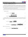
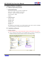
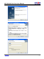
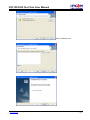
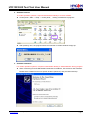
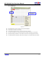
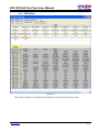
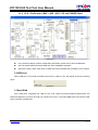
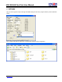
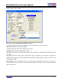
HY313X EVA Test Tool User Manual . © 2011-2012 HYCON Technology Corp www.hycontek.com APD-DMM001-V02_EN Page 1 HY313X EVA Test Tool User Manual Table of Contents 1. DESCRIPTION OF ENOB AND NOISE FREE ..................................................................................................3 2. HARDWARE/SOFTWARE INSTALLATION .....................................................................................................4 3. 2.1 MINIMUM SYSTEM REQUIREMENTS ..................................................................................................................4 2.2 INSTALLATION AND REMOVAL ..........................................................................................................................4 SOFTWARE MENU DESCRIPTION ................................................................................................................. 11 3.1 OPTION ...........................................................................................................................................................12 3.1.1 Setup...............................................................................................................................................................12 3.1.2 RAM Panel ................................................................................................................................................13 3.1.3 REG Panel ................................................................................................................................................14 3.1.4 CLK、ProCounter、MAP、ADS、ADF、OP and POWER Panel ........................................................15 3.2 USB SCAN ......................................................................................................................................................15 3.3 READ RAM ....................................................................................................................................................15 4 ENOB TEST ..........................................................................................................................................................16 5 SETDMM ...............................................................................................................................................................18 6 HARDWARE DESCRIPTION.............................................................................................................................21 . 6.1 USB ENOB TEST BOARD DESCRIPTION .........................................................................................................21 6.2 HY313X DEMO BOARD DESCRIPTION ............................................................................................................22 7 QUESTION OBVIATION ....................................................................................................................................23 8 REVISION RECORD ...........................................................................................................................................24 © 2011-2012 HYCON Technology Corp www.hycontek.com APD-DMM001-V02_EN Page 2 HY313X EVA Test Tool User Manual 1. Description of ENOB and Noise Free RMS Noise that generated from Sigma Delta ADC is the minimum voltage value of distinguishable sampling signal. Hence, ENOB (Effective Number of Bits) is calculated by RMS Noise and Full Scale Range ratio. However, RMS Noise must be calculated by many average times. Insufficient sampling times can only represent RMS Noise for a specific period of time instead of the RMS Noise of the entire ADC operation. Therefore, RMS Noise operation times cannot be less than 1024 times. However, Noise Free Bit represents that ADC output value count is not rolling. Noise Free Bits are stable ADC output performance. Bit operation is defined as Peak-to-Peak Noise and Full Scale Range ratio. RMS Noise Equation: n ADC k 平均 Count → Average = k 1 n (1) 2 n ADC k - Average V k=1 RFE n RMS Noise = Scale 2 (2) In the above equation, n represents total sampling number of ADC and Scale represents ADC total . output bits. ENOB and Noise Free Bits can be gained by taking Equation 1 and Equation 2 to the following equation: ENOB = Log FSR = 2 RMS Noise Noise Free Bits = Log FSR RMS Noise In (3) In 2 FSR = 2 Peak - to - Peak Noise FSR Peak - to - Peak Noise In In 2 (4) Equation of Peak-to-Peak Noise: Peak - to - Peak Noise = © 2011-2012 HYCON Technology Corp www.hycontek.com V ADC - ADC REF Max Min Scale 2 (5) APD-DMM001-V02_EN Page 3 HY313X EVA Test Tool User Manual 2. Hardware/Software Installation 2.1 Minimum System Requirements 1. Hardware Requirements: ® IBM AT/ATX PC PENTIUM or any above compatible type Memory size > 32MB(>256MB is recommended) Resolution > VGA 1024×768, 256-color display Hard discs space > 10MB USB port 2. Operation System Windows™ 98SE Windows™ 2000 Windows™ XP Windows™ Vista Windows™ 7 Not supportive for 64 bit window, *nix and OSX operation system. Menu could be unreadable code when operating in non-traditional Chinese operation system. 2.2 Installation and Removal 1. Software Installation . For certain operation system, it requires Administrator identity to install software to the computer. Look for Setup.exe and execute it from CD-ROM menu or unzip file. Proceeding the installation procedures as frame indicates. As shown in below dialog window. 執行Setup.exe © 2011-2012 HYCON Technology Corp www.hycontek.com APD-DMM001-V02_EN Page 4 HY313X EVA Test Tool User Manual . © 2011-2012 HYCON Technology Corp www.hycontek.com APD-DMM001-V02_EN Page 5 HY313X EVA Test Tool User Manual Select installation path . © 2011-2012 HYCON Technology Corp www.hycontek.com APD-DMM001-V02_EN Page 6 HY313X EVA Test Tool User Manual 2. Software Removal To certain operation systems, it requires Administrator identity to remove software. Control panel(Start → setup → control panel), clicking "install/remove program". 點選新增或 移除程式 After pressing "Yes", the program will be removed but no relative window will pop up. . 3. Software Installation For certain operation systems, it requires Administrator identity to install hardware driving program. When connecting PC and USB ENOB Test Board via USB wire, PC will find a new hardware. Please select "Install from a list or specific location (Advance)" and proceeds next step. © 2011-2012 HYCON Technology Corp www.hycontek.com APD-DMM001-V02_EN Page 7 HY313X EVA Test Tool User Manual Select "Don’t search. I will choose the driver to install" and press next. Click "Have Disk". . Have Disk © 2011-2012 HYCON Technology Corp www.hycontek.com APD-DMM001-V02_EN Page 8 HY313X EVA Test Tool User Manual Click browse and assign driving program menu, the default location is "C:\Program Files\HYDMM\HY3131\Driver\" and press yes. 2. Press Yes 1. Click Browse and assign menu Select "Hycon-USB Temperature Reader Device" and press next. After compatibility warning shows up, please press "continue installation". . 1. Select Hycon-USB Temperature Reader Device 2. Press Next © 2011-2012 HYCON Technology Corp www.hycontek.com APD-DMM001-V02_EN Page 9 HY313X EVA Test Tool User Manual Install complete Installation complete . © 2011-2012 HYCON Technology Corp www.hycontek.com APD-DMM001-V02_EN Page 10 HY313X EVA Test Tool User Manual 3. Software Menu Description Figure 3-1 OPTION: Setup and graphical block diagram USB Scan: USB controller scan Read RAM: Reload registers status SETDMM: Load and calibration setup of DMM ranges ENOB Test: RMS noise and noise free test INTF-Wait/INTF-reading: When ADC under .read status, it must be configured in INTFreading status. ADC will reload data after INTF flag event occurs. © 2011-2012 HYCON Technology Corp www.hycontek.com APD-DMM001-V02_EN Page 11 HY313X EVA Test Tool User Manual 3.1 Option Figure 3-2 Introduce in sequence: 3.1.1 Setup . Figure 3-3 When test tool and HY313X series are connected, the device number and communication mode is set. User needs not to make other selection. © 2011-2012 HYCON Technology Corp www.hycontek.com APD-DMM001-V02_EN Page 12 HY313X EVA Test Tool User Manual 3.1.2 RAM Panel Memory Content Function list shows up after clicking right button of the mouse Figure 3-4 Open RAM window, memory content of the chip will be displayed. If the address is inexistent, it will display -. If the address underlined number, it means Hint has been configured. The data in the address can be directly amended by clicking the left button on the address. By double-clicking the left button on the address, the window of amending data will show up. For detailed operation description, please refer to Chapter 3.2 of HY-IDE software user manual. . © 2011-2012 HYCON Technology Corp www.hycontek.com APD-DMM001-V02_EN Page 13 HY313X EVA Test Tool User Manual 3.1.3 REG Panel . Figure 3-5 Please refer to Chapter 3.3 Register window operation of HY-IDE software user manual. © 2011-2012 HYCON Technology Corp www.hycontek.com APD-DMM001-V02_EN Page 14 HY313X EVA Test Tool User Manual 3.1.4 CLK、ProCounter、MAP、ADS、ADF、OP and POWER Panel Figure 3-6 Every Panel will display relative configuration parameters, please refer to HY3131datasheet. ADC will update data when READ ADC and “INTF-READING” displayed. ADS ADC output is 24bit, after setup via ADS output bits, desirable bits will display on the window. . 3.2 USB Scan When USB port is connected to ENOB control board, “USD On Line” will display as like the following figure: Figure 3-7 3.3 Read RAM After “USB Scan” completed and “USB on Line” was confirmed, please implement Read RAM. The RAM and Registers of chip will be read to the buffer zone of PC. It will affect RMS Noise and Peak-to-Peak Noise operation of ENOB Test. © 2011-2012 HYCON Technology Corp www.hycontek.com APD-DMM001-V02_EN Page 15 HY313X EVA Test Tool User Manual 4 ENOB Test Figure 3-8 1. Sample Point ADC sample point of "Catch ADC" and "ADC-Temp" function. Minimum sample of OTP ADC output is 256 record and maximum is 65536 records. 2. Scale ADC output bit. Minimum ADC output bit is 8-bit and maximum is 24-bit. 3. ENOB . Display ENOB, the calculation is shown as Equation 3, the unit is bit. 4. Noise Free Display Noise Free Bits, as Equation 4, the unit is Bit. 5. Average Display sampling average value of ADC, as Equation 1, the unit is Counts. 6. Vp-p Noise Display Peak-to-Peak Noise, as Equation 5,the unit is nV. 7. RMS Noise Display RMS Noise, as Equation 2, the unit is nV. 8. ADCS、ADCF、AVG、RMS Real time capture and sequence display ADC value in value display zone. 9. Save to CSV Save the display value to *.CSV file, including ENOB, Noise Free, Average, Vp-p Noise and RMS Noise. 10. Change To Chart Switch chart and value in value display zone. 11. Ref Volt © 2011-2012 HYCON Technology Corp www.hycontek.com APD-DMM001-V02_EN Page 16 HY313X EVA Test Tool User Manual Input Reference Voltage (unit: V). 12. Avr. Times Select software average, the value is display zone will perform average again, according to the times of selection and then display in value display zone. . © 2011-2012 HYCON Technology Corp www.hycontek.com APD-DMM001-V02_EN Page 17 HY313X EVA Test Tool User Manual 5 SETDMM User can store register setup file through SETDMM dialog and test every range’s efficiency under calibration status. . First, configure the path to install menu. HYCON offers different range configuration. © 2011-2012 HYCON Technology Corp www.hycontek.com APD-DMM001-V02_EN Page 18 HY313X EVA Test Tool User Manual Take DC 400mV as an example: . After click, it will be highlighted and displayed in blue color. To enhance identification, NAME and calibration unit can be marked by users in word form ADC1 scale: Maximum value after calibration. Calibration Ref: ADC output will be calibrated as ref. value. Select ADC: select ADC1 or RMS output as output Cal. Gain: ADC data of the current network status will be configured as “Calibration Ref” setup after pressing this button. Cal. Offset: Record the current ADC1 or RMS output value as offset. When ”cancel offset” is ticked, ADC1 will deduct offset value and multiply calibration GAIN; RMS will deduct offset first, then perform root and multiply GAIN of RMS. Save Register: Save all registers status in the setup file that is highlighted in blue color. If NO FILE is selected and then save is pressed, one setup file will be added in this menu; however, maximum setup file within a menu is ten. © 2011-2012 HYCON Technology Corp www.hycontek.com APD-DMM001-V02_EN Page 19 HY313X EVA Test Tool User Manual Configure Jump on HY3131 Target Board based on different measurement functions: Function ACV DCV AC mV DC mV Thermocouple AC Current DC Current Resistor Continuity Diode Capacitor Frequency(CNT Input) J2 J6 J17 J8 Short Open Open Open Open Short Open Open Open Open Open A(Open) mA(1-2) uA(2-3) Open Short Open Open Open Short Short Open . © 2011-2012 HYCON Technology Corp www.hycontek.com APD-DMM001-V02_EN Page 20 HY313X EVA Test Tool User Manual 6 Hardware Description Figure 5-1 PC transmits Command to USB ENOB Test Board; USB ENOB Test Board configures and reads ADC value via SPI from Hycon HY310x Demo Board. 6.1 USB ENOB Test Board Description 3 4 4 5 5 6 6 7 7 U9 3 U10 2 U11 2 U12 1 T09011 V02 1 J4 Photo Input Channel J5 2 1 J8 2 1 Photo Power Photo Ground VP SPIDI_Q SPICK_Q SPIDO_Q SPICS_Q VSSP SPIIRQ_Q L1 R3 R2 R1 U6 U3 U7 2 JP1 1 JP2 VBAT J6 VSSBAT . USB power Figure 5-2 1. J4:Optical Coupler SPI Port J4 description PIN 1 → VP, powered by optical coupler IC (U8~U13), J5 and J8 must be opened to completely isolate power. J5 and J8 must be short to use common power supply. PIN 2 → SPIDI_Q, optical coupler DI signal wire. PIN 3 → SPICK_Q, optical coupler CK signal wire. PIN 4 → SPIDO_Q, optical coupler DO signal wire. PIN 5 → SPICS_Q, optical coupler CS signal wire. PIN 6 → VSSP, optical coupler Ground. 2. JP1, JP2, J6, U3:Power Supply Circuit JP1 and JP2 is external power input that supply power to U3 and generates VDD power. Using USB power, J6 is short circuit. Using external 5V power, JP1 and JP2 inputs, J6 is open circuit. Regulated circuit that composed by U3, R1, R2 and R3 generates VDD power. Amending R1, R2 and R3 can change output voltage, the relation is as follows: © 2011-2012 HYCON Technology Corp www.hycontek.com APD-DMM001-V02_EN Page 21 A B C D 1 A P4 mA/uA P3 COM P2 mA uA Current 1 2 3 J8 COM COM R33 0.01 R32 0.99 R1 R22 10K 10K R29 R20 910K R21 C6 C2 0.1uF 2 7.5pF IN U4 AP8841 ML62xx 1 PB1 PB2 PB3 藍框內先不焊接 2 OUT C5 0.1uF + 定位點 JP3 2 C20 2 3 AVSS 7.5pF 2 B B J2 C9 C3 10uF 1 2 3 4 J4 2 3 1 VDD DI CK DO CS VSS Q2 9013 Q1 9013 R26 100 COM AVSS DC9V J3 SPI 1 3 5 7 9 11 JP2 2 4 6 8 10 12 COM R27 10K R23 10M R24 1K R15 1K 0.1% C21 104 R14 10K 0.1% R13 101K 0.1% R12 1.11M 0.1% R7 VDD C4 0.1uF J1 Power Input D4 DC9V 2 100uF C7 GREEN AVSS L1 R11 30K PB0 藍框內先不焊接 PTC R19 10M R10 10M0.7% R18 99 Vol/Ohm/Cap/DT J6 Vol/Ohm/Cap/DT P1 + C1 10uF DC9V 470 DC9V R16 GND 1 8 7 6 5 1 2 3 4 3 E C 11 C E 2 4 37 38 39 40 41 42 43 44 45 46 47 48 R39 R37 R38 R9 1M VDD VSS R2 1M Internal OPA1 Y1 4.9152Mhz PB4 C16 1uF C15 0.1uF OP1O PA9 PA8 PA7 PA6 PA5 PA4 PA3 PA2 PA1 PA0 RLU NC C14 0.1uF 15pF C10 15pF C8 AVSS R28 91K AGND PA8 PA7 PA6 PA5 PA4 PA3 PA2 PA1 PA0 RLU PA9 POWERSEL 1 3 JP1 遠離Analog input VDD DI CK DO CS VSS OP1N R31 AVSS VDDA 3 J9 XOUT J12 XIN HY3131_LQFP48 3 COM R34 10K R8 GROUND 24 23 22 21 20 19 18 17 16 15 14 13 ACM C12 FTN 27nF FTP OP2O OP2N OP1O OP1N R35 PB8 PB0 100K PB1 VDDA PB7 PB2 PB5 PB2 1 PB5 J16 1 J15 COM Digital Power 1 2 3 4 J7 CNT CMP T11001 Number 23-Nov-2012 Y:\MyDesign2011.ddb A4 4 Sheet of Drawn By: COM R3 1M CNT 3 Henry.Cho V01 LM385 D3 PB6 J13 PB6 R17 10K VDDA 2.2p C17 Revision J17 HZ C13 10uF RLD HY3131 Application Board Internal OPA2 1 PB4 J11 1 J10 OP2O 1N4148 PB7 PB4 Date: File: Size Title R30 91K 2 4 CNT/CMP VDD 1 3 J5 C19 C18 1uF 0.1uF AVSS HY3131_LQF P48 AVSS U3 C11 10uF NC FT1N FT1P OP2O OP2N OP1O OP1N PB8 PB0 PB1 VDDA ACM VDD CNT CMP 4 A B C D R3 3 1 1 VSS CNT CMP DO DI CK CS XIN XOUT 36 35 34 33 32 31 30 29 28 27 26 25 NC DVSS CNT CMP DO DI CK CS XIN XOUT NC VDD RLD NC AGND REFO AVSS PB7 PB6 PB5 PB4 PB3 PB2 NC . RLD 1 2 3 4 5 6 7 8 9 10 11 12 REFO AVSS PB7 PB6 PB5 PB4 PB3 PB2 VDD = 1.240V 1 + OP2N 2 1 © 2011-2012 HYCON Technology Corp www.hycontek.com 1 1 HY313X EVA Test Tool User Manual R 1 +R 2 (6) 3. U9, U10, U11, U12: Optical coupler IC components 4. U7:USB Port Port connecting to PC, is the power source of entire system (5V), 500mA input. 6.2 HY313x Demo Board Description APD-DMM001-V02_EN Page 22 HY313X EVA Test Tool User Manual 7 Question Obviation 1. Registers cannot be configured under ADC window? Communication way and IC selection must be configured first. After executing USB Scan and Read RAM, ADC register value can be configured. If USB is connected and confirmed, configuration still cannot be implemented, please close program and remove USB. After plug in the USB, execute the program again. 2. Configuration of ADC window is relatively slow? Please do not change any setup when ADC reads data, this might bring about unpredictable results. 3. Can the data obtained include time? Data obtained from the program includes file that be saved as CSV format but not including time. Users can detect the X axis represents time in graphical display mode, demonstrating in ms. Time recording function will be incorporated in next version of program update. 4. Program cannot be executed, file lack appears and program demands to reinstall. Please print the error window and message and please contact the distributor who provided this DMM EVA Test Tool to you or directly contact HYCON Technology for further support. We are sorry for the inconvenience this has caused to you. . 5. INF error shows up when USB drive program is under installation or is completed and a yellow exclamation mark appears in “device manager”. Please copy all programs of Driver file in the installation menu to c:\windows\system32\drivers. Reinstall driving program again. If error shows up again, please contact the distributor who provided this DMM EVA Test Tool to you or directly contact HYCON Technology for further support. © 2011-2012 HYCON Technology Corp www.hycontek.com APD-DMM001-V02_EN Page 23 HY313X EVA Test Tool User Manual 8 Revision Record Major differences are stated thereinafter: Version Page Revision Summary V01 ALL V02 20 Add in the Table of Target Board Jump of different measurement functions. 22 Add in circuit diagram First edition . © 2011-2012 HYCON Technology Corp www.hycontek.com APD-DMM001-V02_EN Page 24