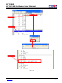
1
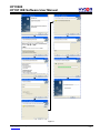
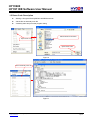
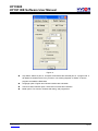
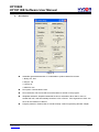
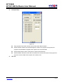
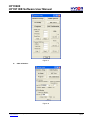
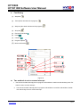
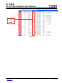
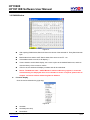
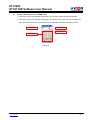
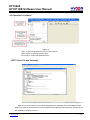
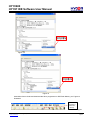
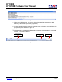
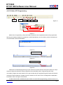
HY13S00 HY13P IDE Software User Manual . © 2012-2013 HYCON Technology Corp. www.hycontek.com APD-HY13PIDE002 _EN HY13S00 HY13P IDE Software User Manual Table of Contents 1.1 INTRODUCTION .............................................................................................................5 1.2 HY13P IDE INSTALLATION AND SYSTEM REQUIREMENT ..................................................5 1.3 INSTALL AND REMOVE ...................................................................................................6 Install ........................................................................................................................................................ 6 Remove..................................................................................................................................................... 8 1.4 REGISTRATION..............................................................................................................8 1.5 DEMO CODE DESCRIPTION ..........................................................................................10 1.6 DEMO CODE OPERATION ............................................................................................. 11 2. HY13P IDE INTERFACE DESCRIPTION......................................................................12 2.1 HY13P IDE EDIT INTERFACE ......................................................................................12 2.1.1Edit Window ................................................................................................................................... 13 2.1.2 File ................................................................................................................................................. 14 2.1.3 Edit................................................................................................................................................. 14 2.1.4View ................................................................................................................................................ 14 2.1.5 Assemble and Run ....................................................................................................................... 15 2.1.6 Interface Setup ............................................................................................................................. 15 2.1.7 Windows........................................................................................................................................ 20 . 2.1.8 Program Structure........................................................................................................................ 20 2.1.9 Self-defined Instruction ............................................................................................................... 21 3. HY13P IDE DEBUG INTERFACE .................................................................................22 3.1 FAST EXECUTION ........................................................................................................23 3.2 RAM WINDOW ...........................................................................................................26 3.3 REGISTER WINDOW ....................................................................................................29 3.4 WATCH WINDOW ........................................................................................................31 3.5 STACK WINDOW .........................................................................................................34 3.6 ADC WINDOW ............................................................................................................35 3.7 COMPARATOR WINDOW ...............................................................................................40 3.8 REGISTER RECORD .....................................................................................................44 3.9 HINT FUNCTION OF SOURCE CODE WINDOW .................................................................46 4. PROGRAMMING WINDOWS........................................................................................48 4.1 INTERFACE SETUP ......................................................................................................48 4.2 OPERATION PROCEDURES ...........................................................................................53 4.2.1 Open File and Assembly.............................................................................................................. 53 4.2.2 Download HEX File....................................................................................................................... 56 4.3 PC ONLINE OTP PROGRAMMING .................................................................................57 © 2012-2013 HYCON Technology Corp www.hycontek.com APD-HY13PIDE002 _EN Page 2 HY13S00 HY13P IDE Software User Manual 4.3.1 Blank Check .................................................................................................................................. 58 4.3.2 Program......................................................................................................................................... 58 4.3.3 Verify.............................................................................................................................................. 59 4.3.4 Read............................................................................................................................................... 59 4.3.5 AUTO.............................................................................................................................................. 61 4.4 OFFLINE PROGRAMMING .............................................................................................62 4.4.1 Programming Description ........................................................................................................... 62 4.4.2 Program Times Restriction ......................................................................................................... 66 5. TROUBLESHOOTING ..................................................................................................66 5.1 HYCON-IDE EXECUTION PROBLEM ............................................................................66 6. REVISION HISTORY.....................................................................................................67 . © 2012-2013 HYCON Technology Corp www.hycontek.com APD-HY13PIDE002 _EN Page 3 HY13S00 HY13P IDE Software User Manual Attention: 1. HYCON Technology Corp. reserves the right to change the content of this datasheet without further notice. For most up-to-date information, please constantly visit our website: http://www.hycontek.com . 2. HYCON Technology Corp. is not responsible for problems caused by figures or application circuits narrated herein whose related industrial properties belong to third parties. 3. Specifications of any HYCON Technology Corp. products detailed or contained herein stipulate the performance, characteristics, and functions of the specified products in the independent state. We does not guarantee of the performance, characteristics, and functions of the specified products as placed in the customer’s products or equipment. Constant and sufficient verification and evaluation is highly advised. 4. Please note the operating conditions of input voltage, output voltage and load current and ensure the IC internal power consumption does not exceed that of package tolerance. HYCON Technology Corp. assumes no responsibility for equipment failures that resulted from using products at values that exceed, even momentarily, rated values listed in products specifications of HYCON products specified herein. 5. Notwithstanding this product has built-in ESD protection circuit, please do not exert excessive static electricity to protection circuit. 6. . Products specified or contained herein cannot be employed in applications which require extremely high levels of reliability, such as device or equipment affecting the human body, health/medical equipments, security systems, or any apparatus installed in aircrafts and other vehicles. 7. Despite the fact that HYCON Technology Corp. endeavors to enhance product quality as well as reliability in every possible way, failure or malfunction of semiconductor products may happen. Hence, users are strongly recommended to comply with safety design including redundancy and fire-precaution equipments to prevent any accidents and fires that may follow. 8. Use of the information described herein for other purposes and/or reproduction or copying without the permission of HYCON Technology Corp. is strictly prohibited. © 2012-2013 HYCON Technology Corp www.hycontek.com APD-HY13PIDE002 _EN Page 4 HY13S00 HY13P IDE Software User Manual 1. HY13P IDE Overview 1.1 Introduction To facilitate the product development process , HYCON-IDE platform is provided to develop the full range of HYCON MCUs. Customers can implement in-circuit emulation of the end-products on this platform and program the code onto OTP products of HY13P series 1.2 HY13P IDE Installation and System Requirement Minimum requirements for operating HY13P IDE: PC Hardware Request: PC compatible system with PENTIUM® CPU 128 MB Memory (256MB is recommended) 10 GB Hard Disk Space Supporting Products: -HY13P56 Supporting Hardware Model No. . -HY13S00-DK01 development kit Supporting Software Version: HY13P IDE V1.0 以上 © 2012-2013 HYCON Technology Corp www.hycontek.com APD-HY13PIDE002 _EN Page 5 HY13S00 HY13P IDE Software User Manual OS: Windows 98SE Windows 2000 Windows XP Windows Vista Windows 7 Applicable Interface: USB Port 1.3 Install and Remove Install Note: For some Windows OS, it may require to have administrator identity to install the Hex Loader to the computer Find and run the file, Setup.exe in the CD ROM or file . Following the instruction window dialogs step by step to continue setup procedures., as shown in Figure 1. . © 2012-2013 HYCON Technology Corp www.hycontek.com APD-HY13PIDE002 _EN Page 6 HY13S00 HY13P IDE Software User Manual . Figure 1 © 2012-2013 HYCON Technology Corp www.hycontek.com APD-HY13PIDE002 _EN Page 7 HY13S00 HY13P IDE Software User Manual Remove Please remove the file of “HY13P IDE” in “Add/Remove Program” under Control Panel. 1.4 Registration For first time using ICE for simulation or program OTP chip, users must apply for a register code as to proceed operation. Figure 2 Registration Procedures: 1. Please check the HY13P IDE Machine Number (HyIDE Code) on the parcel and send the number by e-mail or on-line registration. HYCON will send back another customer register code to you 2. Connect the HyIDE Control Board to PC through USB interface. 3. ExecuteHY13P IDE software (HY13PIDE.exe). Go to ”Option” and press ”Register”. 4. Fill in the customer code in “Register Number” and click “Write” to start. . Figure 3 5. If the process is successful, a dialog will be shown as follows. Figure 4 © 2012-2013 HYCON Technology Corp www.hycontek.com APD-HY13PIDE002 _EN Page 8 HY13S00 HY13P IDE Software User Manual 6. If the process failed, a dialog will be shown as Figure 6 Figure 5 7. Once the register is succeeded, Customers do not have to worry that other numbers may be written into the “Register Number”. . © 2012-2013 HYCON Technology Corp www.hycontek.com APD-HY13PIDE002 _EN Page 9 HY13S00 HY13P IDE Software User Manual 1.5 Demo Code Description Starting C:\Program Files\HyIDE\HY13PIDE\DemoCode. Set the file as assembly main file Assembly starts and proceeds program debug Select kitchFor11P13.asm Open Demo Code Open Demo Code Figure 6 . Set as assembly main file Make sure ICE was connected Display assembly main file name Figure 7 © 2012-2013 HYCON Technology Corp www.hycontek.com APD-HY13PIDE002 _EN Page 10 HY13S00 HY13P IDE Software User Manual Assembly and start debugging Debugging Figure 8 Users can use any compiler to edit Source Code, as long as it can be stored in ASCII Code format. Source code will be reloaded when compiling program to ensure its correctness. Debugging and . edit function will be depicted respectively in the following chapters. 1.6 Demo Code Operation After installing HY13P IDE software, users can refer to Demo Code that provided by HYCON at C:\Program Files\HyIDE\HY13PIDE\DemoCode. © 2012-2013 HYCON Technology Corp www.hycontek.com APD-HY13PIDE002 _EN Page 11 HY13S00 HY13P IDE Software User Manual 2. HY13P IDE Interface Description 2.1 HY13P IDE Edit Interface IDE Software Version IC No. IDE Interface Project Name . Main program file IDE connecting status Checksum after program compiled Figure 9 © 2012-2013 HYCON Technology Corp www.hycontek.com APD-HY13PIDE002 _EN Page 12 HY13S00 HY13P IDE Software User Manual 2.1.1Edit Window Open file Open the existing edited file in the disk Set bookmark Using this function to go back to the bookmark instantly when many files were opened Go to bookmark Jump to the default bookmark Find string Find input string Find next string Go to page Using this function to switch files Assemble Only acting assemble function not debug status. After assembled, a message window will show up . © 2012-2013 HYCON Technology Corp www.hycontek.com APD-HY13PIDE002 _EN Page 13 HY13S00 HY13P IDE Software User Manual 2.1.2 File Figure 10 Open Project Project includes, IC No., IDE interface, main program file name, current status and checksum. The project status will be loaded once this function is activated. 2.1.3 Edit . Figure 11 2.1.4View Figure 12 © 2012-2013 HYCON Technology Corp www.hycontek.com APD-HY13PIDE002 _EN Page 14 HY13S00 HY13P IDE Software User Manual 2.1.5 Assemble and Run Figure 13 Assemble & Run (Emulation) Assemble Source Code and execute debug mode Assemble Only executing assemble, not debugging. Error message will show up when the lines . is error. It is usually used in generating OBJ Code (Object). Set Main File Set the file as assembly main file. Files will be named after compiler generated file name, such as Hex, MAP, ASC…etc. Set Mode (Debug mode) Debug through software or hardware is selective. 2.1.6 Interface Setup Interface Setup © 2012-2013 HYCON Technology Corp www.hycontek.com APD-HY13PIDE002 _EN Page 15 HY13S00 HY13P IDE Software User Manual . Figure 14 Chip Select: Select IC part no. Compiler will assemble the selected part no.’s program file. It will determine whether there is any misuse or non-existing Register or SRAM, or has the program exceeded the ROM Size. Language option: English and Chinese interface are selectable. Communication interface option: Select IDE communication interface. Mode option: Two choices, Emulate and debug, and programmer © 2012-2013 HYCON Technology Corp www.hycontek.com APD-HY13PIDE002 _EN Page 16 HY13S00 HY13P IDE Software User Manual Build Option . Figure 15 Assembler generated extension: it is selectable to produce below file formats. 1. Binary file : Hex 2. Obj file : obj 3. List file: lst 4. ADCII file: asc Font option: Choose editor’s fonts. Fill unused zone: Fill the unused zone with 0x0000 or 0xFFFF in the program. Simplified assemble: Simplified assemble function is selectable. When JMP or CALL is smaller than 2K, it will automatically transform to RJ or RCALL. If the arguments of CALL are set, it will not transform to RCALL. Program protection: Please refer to “Interface Setup” under Programming Window chapter. © 2012-2013 HYCON Technology Corp www.hycontek.com APD-HY13PIDE002 _EN Page 17 HY13S00 HY13P IDE Software User Manual Interrupt Setup . Figure 16 Stop operation when Stack overflow: IDE will stop when Stack overflow. Monitor address: Select the monitored Register or RAM. The program will stop when the program executed RAM or Register value equals to the monitored Data. Monitor Data: Monitor value is set when the monitor Data is filled up. Monitor RAM bit: Monitor function will be activated if the monitor bit is ticked. The program will stop when the bit of Data value equals to the marked on bit. ICE Test © 2012-2013 HYCON Technology Corp www.hycontek.com APD-HY13PIDE002 _EN Page 18 HY13S00 HY13P IDE Software User Manual . Figure 17 OSC calibration Figure 18 © 2012-2013 HYCON Technology Corp www.hycontek.com APD-HY13PIDE002 _EN Page 19 HY13S00 HY13P IDE Software User Manual 2.1.7 Windows The window can be displayed horizontally or vertically. Figure 19 2.1.8 Program Structure Before editing new program, user must select IC part number through interface setup; Different IC will have different Instruction Set, according to IC part number definition; it is classified as H08A and H08B instruction set; User can refer to the appendix software demo code, Chapter 1.6 gives illustration of demo code usage. Users can refer to following program structure to start writing program. Basic structure description is listed as below: Program Name Definition as: ***.ASM Register Name or RAM Definition as: ***.INC There are many program: “Main.asm”, “Initial.asm”, “Interrupt.asm”, . “Sub.asm”, “Mian.inc”, “H08.inc” “Main.asm” structure: ORG 00H JMP BEGIN ; Program name can be any name ; Declare program start ; Jump to main program ORG Include ; Declare interrupt flag address ; Use ”Interrupt.asm” interrupt vice program; ; Max. 100include file. BEGIN: Include JMP … T1: NOP 04H Interrupt.asm Initial.asm T1 ; Main program start. Label name definition can be any word ; Use ”Initial.asm” hardware initial vice program ; Jump to T1 vice program Include Sub.asm ; Use ”Sub.asm” vice program Include Include END 13P.inc Main.inc ;HY13P series special register name, address definition ;RAM name, address definition ; End program Reference Document: IP User Manual: Instruction Set User Manual: H08A Instruction Set Manual or H08B Instruction Set Manual Hycon-IDE Complier User Manual: HY-MCU COMPILER © 2012-2013 HYCON Technology Corp www.hycontek.com APD-HY13PIDE002 _EN Page 20 HY13S00 HY13P IDE Software User Manual 2.1.9 Self-defined Instruction HY13P IDE includes user self-defined instruction function This function provides user to self-define HY13P series instruction as their familiar MCU instructions Usage Description: 1. All self-defined instruction function is installed under: Inst.txt file. It is separated into two rows. The first instruction (first row) of every row is HYCON origin instruction name; users cannot make amendment to it. The second instruction (second row) is "User" self-defined instruction name. 2. First and second instruction can only be separated by space, multi-space or Tab. 3. Second instruction can be followed by semicolon (;) as remark. 4. Second instruction name can be the same as the first one. 5. The name of second instruction cannot be defined as any of HYCON origin instruction name except the instruction in the same row. Otherwise, it is deemed as invalid and will adopt the origin instruction name to compile program. 6. After users self-define the second instruction name, the first or second instruction name can be used when program compiling. 7. Every row can only has one self-defined instruction name, any repeated instruction name will be deemed as invalid. Example: JMP JUMP JMM JPP . JU ; ╳wrong definition Repeated defined instruction or self-define instruction will be deemed as invalid. Example: JMP JUMP JMP JPP ;╳ Instruction name redefine. JUMP is invalid instruction at this point, only JPP is valid. JPP JU JMP JN ;╳ Cannot use self-define name to redefine. ;╳ Cannot define as HYCON existing instruction name. Correct definition is: JMP JUMP © 2012-2013 HYCON Technology Corp www.hycontek.com APD-HY13PIDE002 _EN Page 21 HY13S00 HY13P IDE Software User Manual 3. HY13P IDE Debug Interface It can be classified into hardware debug and software debug: Hardware debug The indication column is blue Software debug The indication column is green . © 2012-2013 HYCON Technology Corp www.hycontek.com APD-HY13PIDE002 _EN Page 22 HY13S00 HY13P IDE Software User Manual 3.1 Fast Execution (1) (3) Fast Window Switch Switch to Edit window Switch to Hex window (2) Switch to Source window (4) Switch to Ram window (6) Switch to Watch window . (5) Switch to Reg window © 2012-2013 HYCON Technology Corp www.hycontek.com APD-HY13PIDE002 _EN Page 23 HY13S00 HY13P IDE Software User Manual Fast Debug (1) Step back (2) Trace (Enter into Macro/vice program) (3) Step over (Not enter into Macro/vice program) (4) Skip Call (5) Execute (Free RUN) (6) Pause (7) Continue (8) Program replace (9) Back to edit mode . Figure 20 Two methods to set or remove interrupt: 1. Use mouse to select interrupt place in program code window or machine code window, press “F2” button to set to remove interrupt. 2. Use mouse to select interrupt place in program code window or machine code window, double click the left key to set or remove interrupt. © 2012-2013 HYCON Technology Corp www.hycontek.com APD-HY13PIDE002 _EN Page 24 HY13S00 HY13P IDE Software User Manual Click mouse to set interval section Figure 22 . © 2012-2013 HYCON Technology Corp www.hycontek.com APD-HY13PIDE002 _EN Page 25 HY13S00 HY13P IDE Software User Manual 3.2 RAM Window Figure 21 After opening RAM window, Bank will show the volume of the selected IC. Every Bank has 256 byte. Bank0 starts from 0x00 to 0xFF. Bank1 starts from 0x100 to 0x1FF…etc. . “-”. If the address does not exist, it will display If users intend to switch Bank display, use cursor to point to the desired Bank zone, and then click the left key of the mouse to confirm. If Hint is set, the address will display numbers and will be underlined. Notice: The Address 0x00 ~ 0x0Eof Bank0 is indirect addressing register, it cannot be revised directly, the displayed value is not referable. If revise is required, please refer to Chapter 3.3. Revise indirect addressing Data or Address. Function Display Click the mouse selection key (right key) Figure 22 Set Mark Set Mark(new color) Reset Mark © 2012-2013 HYCON Technology Corp www.hycontek.com APD-HY13PIDE002 _EN Page 26 HY13S00 HY13P IDE Software User Manual Reset All Mark Set Hint Reset Hint Reset All Hint Load RAM Data Save RAM Data Save To excel RAMBANK0 Hint Use DS defined SRAM; Hint will be automatically generated in corresponding window address. When cursor point to the address, it will show the defined string. Ex: Program definition SRAM MEMAR 080h MD1 DS 1 MD2 DS 1 MD3 DS 1 MDL1 DS 1 MDL2 DS 1 MDL3 DS 1 MD4 DS 5 S_REG DS 1 r_Len DS 1 SQRTmp DS 4 . Temp DS 16 After assembling, it will enter into debug status, displaying memory window. When cursor points to 80h address, <80>:MD1 will be shown. When cursor points to 86h address, <86>:MD4[0] will show up. When cursor points to 87h address, <87>:MD4[1] will show up. Figure 23 © 2012-2013 HYCON Technology Corp www.hycontek.com APD-HY13PIDE002 _EN Page 27 HY13S00 HY13P IDE Software User Manual There are two ways to revise SRAM value: 1. Point the cursor to the selected revised lines, click mouse’s left key and Key IN directly. 2. Point the cursor to the selected revised lines, double click the mouse’s left key, a window will pop up as Figure 27 shown. Users can key in on keyboard or press the button by mouse RAM Data RAM Address Keyboard Key IN Mouse Click Figure 24 . © 2012-2013 HYCON Technology Corp www.hycontek.com APD-HY13PIDE002 _EN Page 28 HY13S00 HY13P IDE Software User Manual 3.3 Register Window WREG Program Counter Cycle Times 間接定址0的Data 間接定址0的Address 間接定址1的Address 間接定址0的Data 單一Byte的Register 1個Word組成的 Register 顯示PAGE1 Register 顯示PAGE2 Register 顯示PAGE3 Register Register byte . Register bit Figure 25 Modify Indirect Data or Address As Figure 269 configures, using keyboard to Key IN or using cursor to click data the Address can be modified Figure 26 As shown in Figure 27, using Key IN of the keyboard or using cursor to click data the Data can be modified. © 2012-2013 HYCON Technology Corp www.hycontek.com APD-HY13PIDE002 _EN Page 29 HY13S00 HY13P IDE Software User Manual Figure 27 Modify WREG Data Figure 28 Modify single 1byte or Word Register Data . Double click the mouse’s left key, a input interface will show up Click Zone Using keyboard to Key In directly Figure 29 Modify Register single 1 byte or single 1 bit After configuring Bit as 1, it will be highlighted in white, blue digit After configuring Bit as 0, it will be marked in black digit © 2012-2013 HYCON Technology Corp www.hycontek.com APD-HY13PIDE002 _EN Page 30 HY13S00 HY13P IDE Software User Manual Double click mouse left key Double click mouse left key Number input window shows up Number input window shows up Figure 30 3.4 Watch Window . Figure 31 Watch Name Monitor Data name, program uses EQU or DS defined name Watch Address Monitor Data Address Watch Data Display value, can select display arrangement from right to left or from left to right or in decimal or hexadecimal system. 4 options will show up after clicking Move the mouse to here and double clicking Figure 32 Hex (H L): Hexadecimal display, address H/L from low to high Hex (L H): Hexadecimal display, address L/H from high to low Dec (H L): Decimal display, address H/L from low to high Dec (L H): Decimal display, address L/H from high to low © 2012-2013 HYCON Technology Corp www.hycontek.com APD-HY13PIDE002 _EN Page 31 HY13S00 HY13P IDE Software User Manual Watch Data for Bin Data display in decimal system, only show up when using EQU defined address Data Length Data length, display DS definition length; it will display 2 when using EQU definition Data Type D = DS definition; C = EQU definition . © 2012-2013 HYCON Technology Corp www.hycontek.com APD-HY13PIDE002 _EN Page 32 HY13S00 HY13P IDE Software User Manual Monitor EQU defined Register or RAM, click right key of the mouse and select the register or RAM to be monitored, as shown in Figure 33. Figure 33 . © 2012-2013 HYCON Technology Corp www.hycontek.com APD-HY13PIDE002 _EN Page 33 HY13S00 HY13P IDE Software User Manual 3.5 Stack Window Figure 34 . Figure 35 © 2012-2013 HYCON Technology Corp www.hycontek.com APD-HY13PIDE002 _EN Page 34 HY13S00 HY13P IDE Software User Manual 3.6 ADC Window Click ADC Panel Figure 36 ADC Sample Clock ENLDO ENADC VDDA Network DC Offset Network ADGN Network . INH Network VRGN ENAD1HS ENCHOP1 OSR Network IN1ST Display ADC Data Select ADC output format ADC output Bits INL Network Display ADC output button PGA Network VRH Network VRL Network VR1ST Figure 37 IN1P Network (1) Click mouse left key on the name of INH, to select INH network. (2) Click mouse left key on the network switch, INH to select the network. (3) Click mouse left key, window like Figure 38 will appear, users can select network switches. © 2012-2013 HYCON Technology Corp www.hycontek.com APD-HY13PIDE002 _EN Page 35 HY13S00 HY13P IDE Software User Manual Figure 38 IN1N Network (4) Click mouse left key on the name of INL, to select INL network. (5) Click mouse left key on the network switch, INL to select the network. (1) Click mouse left key, window like Figure 382 will appear, users can select network switch. Figure 39 IN1ST Switch . (1) Click mouse left key on the name of IN1ST, switch will be ON/OFF (2) Click mouse left key on the network switch, IN1ST switch will be ON/OFF VR1P Network (1) Click mouse left key on the name of VR1P to select the network (2) Click mouse left key on the network switch, VR1P to select the network (3) Click mouse left key on the network, window like Figure 40 will appear, users can select network switch. Figure 40 VR1N Network (1) Click mouse left key on the name of VR1N to select the network (2) Click mouse left key on the network switch, VR1N to select the network (3) Click mouse left key on the network, window like Figure 40 will appear, users can select network switch © 2012-2013 HYCON Technology Corp www.hycontek.com APD-HY13PIDE002 _EN Page 36 HY13S00 HY13P IDE Software User Manual Figure 41 ADC Sample Clock Click mouse left key, window like Figure 42 will show up, and then user can select the network switch Figure 42 ENADC Click mouse left key on network switch, ENADC will be ON/OFF. When ENADC = ON, ADC display zone will show value. VDDA Network ENVDDA control . (1) Select ENVDDA switch ON/OFF (2) Select VDDA voltage Click mouse left key, window like Figure 43 will show up, users can select to the mode. Figure 43 (3) Display VDDA voltage When ENVDDA = 0, the zone display VDDA = External When ENVDDA = 1, the zone display VDDX select voltage PGA Network Click mouse left key, window like Figure 44 will show up, users can select to the network. Figure 44 VRH Network (1) Click mouse left key to the network name, VRH, to select the network (2) Click mouse left key to the network switch, VRH, to select the network. © 2012-2013 HYCON Technology Corp www.hycontek.com APD-HY13PIDE002 _EN Page 37 HY13S00 HY13P IDE Software User Manual (3) Click mouse left key, window likeFigure 45 will show up, users can select to the switch network. Figure 45 VRL Network (1) Click mouse left key to the network name, VRL, to select the network (2) Click mouse left key to the network switch, VRL, to select the network. (3) Click mouse left key, window likeFigure 45 will show up, users can select to the switch network Figure 46 DC Offset Network . Click mouse left key, window likeFigure 45 will show up, users can select to the network. Figure 47 ADGN Network Click mouse left key, window likeFigure 45 will show up, users can select to the network. Figure 48 VR1GN Click mouse left key to the network name, VR1GN, to select the network OSR Network Click mouse left key, window likeFigure 45 will show up, users can select to the network © 2012-2013 HYCON Technology Corp www.hycontek.com APD-HY13PIDE002 _EN Page 38 HY13S00 HY13P IDE Software User Manual Figure 49 ADC Display Zone (1) Select ADC output form Hex or Dec output is selectable (2) Select ADC output Bit 8 ~ 24 Bit output is selectable (3) Display output button clicking this button to display ADC output value . © 2012-2013 HYCON Technology Corp www.hycontek.com APD-HY13PIDE002 _EN Page 39 HY13S00 HY13P IDE Software User Manual 3.7 Comparator Window Mouse click comparator window Figure 50 MCRPS Network MCOHS Voltage Divider Select MCRS Select MCNS Network ENMC Switch . MCOIV Switch MCNES Network MCOFR Switch MCLP Switch MCNEC Switch MCPS Network MCSR Switch Figure 51 MCNES Network (1) Click mouse left key to the network name, CPIH, to select the network (2) Click mouse left key to the network switch, MCNES to select the network (3) Click mouse left key, window like Figure 52 shows up, then user can select the switch network © 2012-2013 HYCON Technology Corp www.hycontek.com APD-HY13PIDE002 _EN Page 40 HY13S00 HY13P IDE Software User Manual Figure 52 MCRPS Network (1) Click mouse left key to the network name, MCRPS, to select the network (2) Click mouse left key to the network switch, MCRPS, to select the network (3) Click mouse left key, window like Figure 53 shows up, then user can select the switch network Figure 53 MCOHS Network (1) Click mouse left key to the network name, MCOHS, to select the network . (2) Click mouse left key to the network switch, MCOHS, to select the network (3) Click mouse left key, window like Figure 54 shows up, then user can select the switch network Figure 54 MCRS Network (1) Click mouse left key to the network name, MCRS, to select the network (2) Click mouse left key to the network switch, MCRS, to select the network (3) Click mouse left key, window like Figure 55 shows up, then user can select the switch network © 2012-2013 HYCON Technology Corp www.hycontek.com APD-HY13PIDE002 _EN Page 41 HY13S00 HY13P IDE Software User Manual Figure 55 MCNS Network (1) Click mouse left key to the network name, MCNS, to select the network (2) Click mouse left key to the network switch, MCNS, to select the network (3) Click mouse left key, window like Figure 56 shows up, then user can select the switch network Figure 56 MCPS Network . (1) Click mouse left key to the network name, MCPS, to select the network (2) Click mouse left key to the network switch, MCPS, to select the network (3) Click mouse left key, window like Figure 57 shows up, then user can select the switch network Figure 57 © 2012-2013 HYCON Technology Corp www.hycontek.com APD-HY13PIDE002 _EN Page 42 HY13S00 HY13P IDE Software User Manual VDDA Network (Please refer to ADC VDDA network) ENMC Click mouse left key to the network name, ENMC starts ENMC status display When ENMC = 1, enable comparator When ENMC = 0, disable comparator MCLP Click mouse left key to the network name, MCLP starts MCLP status display When MCLP = 1, high power consumption and high performance When MCLP = 0, low power consumption mode MCOFR Enable Click mouse left key to the network name, MCOFR module will be enabled or disabled MCOFR status display When MCOFR = 1, enable output filter module When MCOFR = 0, disable output filter module MCOIV Switch Click mouse left key to the network name, MCOIV will be ON/OFF MCOIV status display . When MCOIV = 1, non-inverting When MCOIV = 0, inverting MCNEC Switch Click mouse left key to the network name, MCNEC will be ON/OFF MCNEC status display When MCNEC = 1, according to CCK_D1, doing open/close serial movement When MCNEC = 0, both open circuit © 2012-2013 HYCON Technology Corp www.hycontek.com APD-HY13PIDE002 _EN Page 43 HY13S00 HY13P IDE Software User Manual 3.8 Register Record If the register or SRAM has been revised manually after access to simulation window (hardware emulation or software simulation), the data will be recorded (no matter RAM, Register, ADC, OP and CMP was revised by which window). The data will be revealed after pressing the button “SRAM record”. At this time, windows will suspend until it is closed to execute other commands. Display SRAM & Register Record . Display Save or Clear Status Display continue or discontinue status Figure 58 © 2012-2013 HYCON Technology Corp www.hycontek.com APD-HY13PIDE002 _EN Page 44 HY13S00 HY13P IDE Software User Manual Add in program PC stop address . New added program Figure 59 © 2012-2013 HYCON Technology Corp www.hycontek.com APD-HY13PIDE002 _EN Page 45 HY13S00 HY13P IDE Software User Manual 3.9 Hint Function of Source Code Window If users intend to know Register, SRAM value and Address in source code window, point the cursor to Register or SRAM, the name, address and data can be revealed. This function is only applicable to the instructions below: CLRF, ADDF, INF, INSZ, DCF, DCSZ, SUBF, COMF, ADDC, ANDF, IORF, XORF, SUBC, RRF, SETF, MULF, RLF, JZ, RRFC, RLFC, SWPF, DAW, INSUZ, DCSUZ, ARLC, ARRC, CPSG, CPSL, CPSE, TFSZ, BTFG BSF, BCF, BTSS, BTSZ, MVFF(不是Macro)。 Only the first parameter is effective when instruction is under byte operation, as Figure 603 described. When command is BCF, BSF, BTSS, BTSZ and BTGF, Byte value will be revealed if the cursor points to the first argument. If the cursor points to the second argument, it will display the specified Bit value (1 or 0) as Figure 614 illustrated. When command is MVFF (not Macro), the first argument value will appear if the cursor points to the first argument. If the cursor points to the second argument, the argument value will show up as shown in Figure 62. If the argument is INDF0, POINC0, PODEC0, PRINC0, INDF1, POINC1, PODEC1 and PRINC1, the Data will be FSR0 or the address Data of FSR1 as Figure 63 described. If the argument is PLUSW0 or PLUSW1,. the Data is FSR0+WREG or the address Data of FSR1+WREG as illustrated in Figure 64. Figure 60 Figure 61 © 2012-2013 HYCON Technology Corp www.hycontek.com APD-HY13PIDE002 _EN Page 46 HY13S00 HY13P IDE Software User Manual Figure 62 Figure 63 . Figure 64 © 2012-2013 HYCON Technology Corp www.hycontek.com APD-HY13PIDE002 _EN Page 47 HY13S00 HY13P IDE Software User Manual 4. Programming Windows 4.1 Interface Setup Click “Options”, a window will appear. Click the interface setup, as shown in Figure 65. Click Option Click Interface Setting Select Chip No. Select Language Select Interface Select Programming Mode . Figure 65 Chip Select Choose the specific programming IC part no. If programmed IC part no. differs from that of the selected IC, Blank Check, Program and Verify will fail. Language Choose operation interface language, like Chinese or English. Hardware Interface USB interface or Parallel Port interface is selectable. IDE Mode Programmer or emulate and Debug is selectable. When interface setup finished, click Build Options to select programming configuration. As described in Figure 66. © 2012-2013 HYCON Technology Corp www.hycontek.com APD-HY13PIDE002 _EN Page 48 HY13S00 HY13P IDE Software User Manual . Figure 66 © 2012-2013 HYCON Technology Corp www.hycontek.com APD-HY13PIDE002 _EN Page 49 HY13S00 HY13P IDE Software User Manual Generate Files Choose generated file after assembly Stack Option Choose whether to reset when stack overflow or stack full after OTP program operation. No Use Area Fill Fill up 00 or FF in unused program space after assembly. Smart Compiler Choose whether to simplify assembly. Enable Program Times Choose whether to enable Download program times. Input Program Times Input Download program times (Maximum: 2147483646. Minimum: 1). After assembly finished, click “ICE Test” to test ICE operation voltage as Figure 67 (Connect Adapter 9V and connect USB Line to ICE. Make sure the ICE is connected, and then click “Option”). . Figure 67 VPP voltage when programming: 5.6<VPP<6.6 VDD voltage when programming: 2.7<VDD<3.6 After voltage testing completed, click ”OSC Calibration” to software/hardware frequency calibration. Notice of using this function: If software HAO/LPO calibration programming is activated, RAM 0FEH/0FFH address data will be meaningful after powering up the IC. Single site programming time will increase about 500msec (software LPO calibration programming is enabled) Software HAO/LPO calibration function is not actual calibration frequency, only providing frequency deviation for calculation. Online programming only support hardware calibration, HAO, not software calibration function. © 2012-2013 HYCON Technology Corp www.hycontek.com APD-HY13PIDE002 _EN Page 50 HY13S00 HY13P IDE Software User Manual Figure 68 HAO Calibration: Enable H/W Calibration:Enable hardware HAO calibration function, actually calibrates system frequency. Hardware calibration function must be confirmed after choosing IC part no. . Enable S/W Calibration:Enable software HAO deviation calibration function. Deviation stores at RAM 0FEH address. LPO Calibration: Enable S/W Calibration:Enable software LPO deviation calibration function. Deviation stores at RAM 0FFH address. Input HAO or Input LPO:Frequency value to be calibrated. Permissible Error:Permissible range of frequency value after calibrated and to be calibrated. Software calibration will be described in below: HAO Software Calibration: Frequency deviation value was stored at RAM 0FEH. Deviation will be written to RAM when IC Power on. This action is not actual frequency calibration source. HAO Hardware Calibration and HAO Software Calibration can be co-existed. Executing Hardware Calibration first, then to calculate Software Calibration. HAO deviation basic frequency is defined as 4000HZ/LSB. Data format of OFEH address: Bit7:0= +, 1= -; Bit6~Bit0 represents frequency differences 01H represents frequency difference is +4000HZ while FFH represnets -4000HZ; Example: HAO is about to calibrate 2000000HZ frequency, and the actual IC HAO=1920000HZ. Then (1920000-2000000)/4000 = -80000/4000= -20. Thus the RAM 0FEH data is 1110 1100b © 2012-2013 HYCON Technology Corp www.hycontek.com APD-HY13PIDE002 _EN Page 51 HY13S00 HY13P IDE Software User Manual Example1: HAO is about to calibrate 2000000HZ frequency, and the actual IC HAO=2008000HZ. Then (2008000-2000000)/4000 = 8000/4000=2. Thus the RAM 0FEH data is 0000 0010b LPO Software Calibration: The calculated frequency deviation stores at RAM 0FFH address and will be written to RAM after IC Power on. This action is not actual calibration frequency source. LPO deviation basic frequency is defined as 64HZ/LSB. OFFH address data format: Bit7: 0= +, 1= -;Bit6~Bit0 represents frequency differences; 01H represents frequency value as +64HZ;FFH represents frequency value as -64HZ; Example: LPO is about to calibrate 28000HZ frequency, and the actual IC LPO=28128HZ. Then (28128-28000)/64 = 128/64 = 2. Thus RAM 0FFH data is 0000 0010b Example1: LPOs about to calibrate 28000HZ frequency, and the actual IC LPO=27872HZ. Then (27872-28000)/64 = -128/64 = -2. Thus RAM 0FFH data is 1111 1110b After the completion of interface setup, click close. All configured parameters will be recorded and . reloaded automatically when initiated next time. Title window will show the defaulted programming IC part no., as shown in Figure 69. Show chip no. to be programmed Figure 69 © 2012-2013 HYCON Technology Corp www.hycontek.com APD-HY13PIDE002 _EN Page 52 HY13S00 HY13P IDE Software User Manual 4.2 Operation Procedures Figure 70 Open Open the programmed source code main file. Open Project Open the saved project. Save Project Save the finished project. 4.2.1 Open File and Assembly . Figure 71 Open source code main file and it will be displayed as the assembly file. If the displayed name differs from main file, points the mouse to the specific file and presses mouse right key. Set this file as the assembly main file as shown in © 2012-2013 HYCON Technology Corp www.hycontek.com APD-HY13PIDE002 _EN Page 53 HY13S00 HY13P IDE Software User Manual Figure 72. . Figure 72 Assembles Source Code and download the file to programmer or IDE Flash Memory, as Figure 73 illustrated. Assemble and Download to IDE Flash Memory Figure © 2012-2013 HYCON Technology Corp www.hycontek.com APD-HY13PIDE002 _EN Page 54 HY13S00 HY13P IDE Software User Manual 73 Figure 74 1. When using USB interface, the program code will be loaded into programmer or Flash Memory of IDE for mass production programming. 2. If there is enabled program times in the assembly option, information column will display the programming times as shown in Figure 74. 3. After assembling completed, Hex filename and Checksum will be displayed in underneath section, as Figure 75 illustrated. Loading Hex file name Chip Connection Status Hex Checksum . Figure 75 © 2012-2013 HYCON Technology Corp www.hycontek.com APD-HY13PIDE002 _EN Page 55 HY13S00 HY13P IDE Software User Manual 4.2.2 Download HEX File To download Hex File, please use HY13P-Hex Loader software and operate according to the user manual. HY-Hex Loader Software User Manual . © 2012-2013 HYCON Technology Corp www.hycontek.com APD-HY13PIDE002 _EN Page 56 HY13S00 HY13P IDE Software User Manual 4.3 PC Online OTP Programming Show Code Blank Check Assemble Verify Auto Read Figure 76 Figure 77 Blank Check, Programming, Verify and Read Commands can be implemented when the programmed file being successfully loaded into programmer or IDE Flash Memory. On the contrary, those commands will not be activated if the download failed. . Figure 78 OTP on Figure 79 OTP not connected Figure 80 Make sure the selected programming IC part number is the same with the OTP part number in the topic window as Figure 65 described. When programmer executes Blank Check, Programming and Verify commands, program will check whether the IC part number and OTP programming part number are identical. If the part number is different, the data will not be written into OTP and an error message will be displayed in information column as Figure 78 described. If users intend to find out whether the part number is correct before programming, point the cursor to ”IC © 2012-2013 HYCON Technology Corp www.hycontek.com APD-HY13PIDE002 _EN Page 57 HY13S00 HY13P IDE Software User Manual Connection Status Display” and click the mouse left key. If the selected IC is correct, a message will show up as Figure 79. If it is incorrect, the message will be displayed as Figure 83. If “Enable Program Times” has been marked up, the spare program times will display in the message column as Figure 81 illustrated. Figure 81 4.3.1 Blank Check Blank Check icon is . The internal code of Blank ICs that have yet been programmed is 0xFFFF. The purpose of checking the IC is to make sure the OTP address content is 0xFFFF. If the IC selection is correct and the content is empty, a message will appear as Figure 82 Figure 82 If the IC selection is incorrect or the content is not empty, a message will show up as Figure 83. . Figure 83 4.3.2 Program The icon of Program is . The purpose of programming is to write Compiler accomplished program into IC OTP. When programming is completed and the IC is assembled as finished goods, programmer can operate the program as user commanded. Program the downloaded or assembly finished Hex file (displayed at the bottom of the column) in the selected IC and verify the correctness of the programming content (please refer to Chapter 4.2.1 or 4.2.2 for programming procedures). If the selected IC is correct and the programming succeeds, message will appear at the information column as Figure 84 illustrated. If “Enable Program Times” is ticked up, the enable program times will minus 1 and the program times left will be revealed in the message column. © 2012-2013 HYCON Technology Corp www.hycontek.com APD-HY13PIDE002 _EN Page 58 HY13S00 HY13P IDE Software User Manual 剩餘的燒錄 如果有勾選 ”Enable Program Times” 次數 Figure 84 If the IC selection is incorrect or the programming fails, a message will show up as Figure 85. Figure 85 4.3.3 Verify The icon of Verify is . The purpose to verify programming IC is to compare if the program written into IC OTP equals to the program downloaded to programmer or IDE Flash Memory. Verify programming IC content consistency with the downloaded or assembled Hex file (displayed at the . bottom of the column). If the IC is protected by program, this verification is ineffective or the comparison failed. If IC selection and program verification is success, a message will appear as Figure 86. Figure 86 f IC selection is incorrect or the program verification miscarries, a message will pop up as Figure 87. Figure 87 4.3.4 Read The icon of Read is . The purpose to read the IC is to verify the consistency of OTP Checksum and programmed Hex file. To read IC content, the procedures are illustrated as Figure 88. Its content will reveal at ”Display Code” window.。 © 2012-2013 HYCON Technology Corp www.hycontek.com APD-HY13PIDE002 _EN Page 59 HY13S00 HY13P IDE Software User Manual Show OTP Code Show OTP Checksum Figure 88 . © 2012-2013 HYCON Technology Corp www.hycontek.com APD-HY13PIDE002 _EN Page 60 HY13S00 HY13P IDE Software User Manual 4.3.5 AUTO The icon of Auto is . Auto integrates Blank Check, Program and Verify function. If user selects Auto, it will first check whether the IC is blank, then to program and verify. After the execution succeeded, a message will be displayed as Figure 89 displayed. If the option, ”Enable Program Times” is ticked up, the program permitted times will reduce 1 and the program times left will be shown in the message column. Figure 89 If any function fails, the whole process will stop and display an error message in the message column. . © 2012-2013 HYCON Technology Corp www.hycontek.com APD-HY13PIDE002 _EN Page 61 HY13S00 HY13P IDE Software User Manual 4.4 Offline Programming 4.4.1 Programming Description As the development process evolves to engineering trial production, the programmer can be used alone. It is not necessary to connect programmer to PC. 9V Ground U20 J14 JP3 ICESDO ICESDI ICEC VDD ICESCK VSS 1 2 3 4 5 6 HY13P. ICE USB Control Board D11 D10 D9 P3 S5 Blank Check S4 1 2 3 4 Program VPP (6V) ICESCK ICESDI ICESDO 5 VDD (3V) 6 VSS Figure 90 J14 : Adapter 9V input supply programming power source, connected when programming OTP U20 : USB connector to PC Downloading program for emulation and debug Downloading programming code for HY13P series P3 : HY13P series programming control port PIN 1 VPP(6V) connects to VPP PIN 2 ICECK connects to PSCK PIN 3 ICESDI connects to PSDI © 2012-2013 HYCON Technology Corp www.hycontek.com APD-HY13PIDE002 _EN Page 62 HY13S00 HY13P IDE Software User Manual PIN 4 ICESDO connects to PSDO PIN 5 VDD(3V) connects to VDD PIN 6 VSS connects to VSS S4 : Program, IC programming button S5 : Blank Check, Blank Check key D9 Green LED:USB or Adapter power on, OTP programming, Blank Check…successful execution display light D10 Red LED:OTP programming, Blank Check, frequency calibration… error execution display light D11 Red LED: Under programming . © 2012-2013 HYCON Technology Corp www.hycontek.com APD-HY13PIDE002 _EN Page 63 HY13S00 HY13P IDE Software User Manual Figure 91 shows the connection way of connecting programming IC to control board programming pin when PC online: Figure 91 Figure 92 shows the connection way of connecting offline programming IC to control board programming pin when PC offline: . Figure 92 To implement offline operation, Hex file must be firstly downloaded to programmer Flash Memory. The procedure can refer to chapter 4.2.1 or chapter 4.2.2. To implement offline operation, press S5 button to check if the IC is blank and the D9 Green LED should be lighted up. S4 Button is programming button. Its procedures are: Blank Check Program Verify. If ”Program Protection” of “Assemble Option” is ticked before downloading data to Flash Memory, © 2012-2013 HYCON Technology Corp www.hycontek.com APD-HY13PIDE002 _EN Page 64 HY13S00 HY13P IDE Software User Manual program protection will be executed after Verify completed. If ”Program Protection” is not picked up, it will stop after Verify accomplished and D4 Green LED will be lighted up. When Programming finished, please press S5 to check if the IC is blank. At this moment, the D10 Red LED should be lighted up, which means the programming is successful (data has been programmed into IC, so Blank Check failed). If any failure or error happened during execution procedures, D10 Red LED will be lightened up. On the contrary, D9 Green LED will be lighted up if success. . © 2012-2013 HYCON Technology Corp www.hycontek.com APD-HY13PIDE002 _EN Page 65 HY13S00 HY13P IDE Software User Manual 4.4.2 Program Times Restriction The menu of Assemble Option in interface setup has an option of Enable Program Times as described Figure 66. This option restricts the permitted program times of download program. This is a safety mechanism that restrains the permitted program times, preventing it from over-programming on the production line. After ticking up Enable Program Times, key in the program times in the column below Input Program Times (maximum is 99999999, minimum is 1). This argument will be written into EEPROM of the programmer after the compiler programmed file is downloaded to Flash Memory. Afterwards, the enabled program times will reduce 1 each time when programming completed. If the value reduced to 0, the programming action may not be executed. At this time, an error signal (Red LED) will be lighted up but Blank Check still operates normally. 5. Troubleshooting 5.1 HYCON-IDE Execution Problem . The problem might be happened under Microsoft Vista or Windows 7 system environment. To avoid the problem, the limit of authority for HYCON-IDE execution has to be set as system administrator to execute HYCON-IDE by administrator status. © 2012-2013 HYCON Technology Corp www.hycontek.com APD-HY13PIDE002 _EN Page 66 HY13S00 HY13P IDE Software User Manual 6. Revision History Major differences are stated thereinafter: Version Page Revision Summary V01 ALL First Edition . © 2012-2013 HYCON Technology Corp www.hycontek.com APD-HY13PIDE002 _EN Page 67