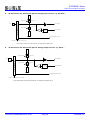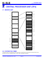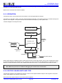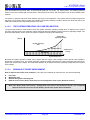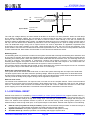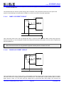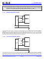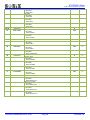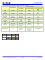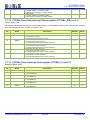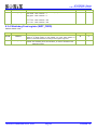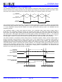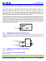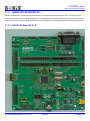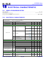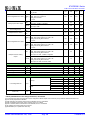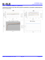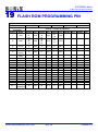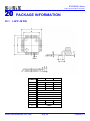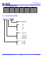
1
SN32F100 Series 32-Bit Cortex-M0 Micro-Controller SN32F100 Series USER’S MANUAL SN32F107 SN32F108 SN32F109 SONiX 32-Bit Cortex-M0 Micro-Controller SONIX reserves the right to make change without further notice to any products herein to improve reliability, function or design. SONIX does not assume any liability arising out of the application or use of any product or circuit described herein; neither does it convey any license under its patent rights nor the rights of others. SONIX products are not designed, intended, or authorized for us as components in systems intended, for surgical implant into the body, or other applications intended to support or sustain life, or for any other application in which the failure of the SONIX product could create a situation where personal injury or death may occur. Should Buyer purchase or use SONIX products for any such unintended or unauthorized application. Buyer shall indemnify and hold SONIX and its officers, employees, subsidiaries, affiliates and distributors harmless against all claims, cost, damages, and expenses, and reasonable attorney fees arising out of, directly or indirectly, any claim of personal injury or death associated with such unintended or unauthorized use even if such claim alleges that SONIX was negligent regarding the design or manufacture of the part. SONiX TECHNOLOGY CO., LTD Page 1 Version 1.4 SN32F100 Series 32-Bit Cortex-M0 Micro-Controller AMENDENT HISTORY Version 1.0 1.1 Date 2013/03/18 2013/03/29 1.2 2013/04/02 1.3 2013/06/04 1.4 2013/07/16 Description First version released. 1. Update Codec Spec. 2. Update DAC Setting 3 Register. 3. Update Sigma-delta DAC Power-Up Sequence. 1. Update Codec Spec. 2. Update ADC Setting 23 Register. 3. Update DAC Setting 1 Register and DAC Setting 2 Register. 1. Add SN32F100 Start Kit V1.1 description. 2. Add Comparator Output Debounce Time. 3. Update supply current. 4. Add Operation Mode Comparison Table. 5. Update System Block Diagram. 6. Update System Tick Timer description. 7. Update LQFP 64 Pin Package Information. 8. Update Comparator description. 9. Modify ADC’s SEL_MIC definition. 1. Update I2S’s Status register default value. 2. Update ADC’s SEL_MIC register default value. 3. Update Code Security diagram. 4. Update Code Option Table. 5. Update High-level and Low-level input voltage Spec. 6. Update P0.14/DPDWAKEUP pin description. SONiX TECHNOLOGY CO., LTD Page 2 Version 1.4 SN32F100 Series 32-Bit Cortex-M0 Micro-Controller Table of Content AMENDENT HISTORY ................................................................................................................................ 2 11 22 PRODUCT OVERVIEW ....................................................................................................................... 13 1.1 1.2 1.3 1.4 1.5 FEATURES ...................................................................................................................................... 13 SYSTEM BLOCK DIAGRAM ........................................................................................................ 15 CLOCK GENERATION BLOCK DIAGRAM ................................................................................ 16 PIN ASSIGNMENT ......................................................................................................................... 17 PIN DESCRIPTIONS ....................................................................................................................... 20 1.6 PIN CIRCUIT DIAGRAMS ............................................................................................................. 25 CENTRAL PROCESSOR UNIT (CPU) .............................................................................................. 27 2.1 MEMORY MAP ............................................................................................................................... 27 2.2 SYSTEM TICK TIMER ................................................................................................................... 27 2.2.1 OPERATION ............................................................................................................................ 28 2.2.2 SYSTICK USAGE HINTS AND TIPS ....................................................................................... 28 2.2.3 SYSTICK REGISTERS .............................................................................................................. 29 2.2.3.1 System Tick Timer Control and Status register (SYSTICK_CTRL) ................................... 29 2.2.3.2 System Tick Timer Reload value register (SYSTICK_LOAD) ........................................... 29 2.2.3.3 System Tick Timer Current Value register (SYSTICK_VAL) ............................................ 29 2.2.3.4 System Tick Timer Calibration Value register (SYST_CALIB) ......................................... 30 2.3 NESTED VECTORED INTERRUPT CONTROLLER (NVIC) ..................................................... 31 2.3.1 INTERRUPT AND EXCEPTION VECTORS ........................................................................... 31 2.3.2 NVIC REGISTERS .................................................................................................................... 31 2.3.2.1 IRQ0~31 Interrupt Set-Enable Register (NVIC_ISER) ....................................................... 32 2.3.2.2 IRQ0~31 Interrupt Clear-Enable Register (NVIC_ICER) ................................................... 32 2.3.2.3 IRQ0~31 Interrupt Set-Pending Register (NVIC_ISPR) ..................................................... 32 2.3.2.4 IRQ0~31 Interrupt Clear-Pending Register (NVIC_ICPR) ................................................. 32 2.3.2.5 IRQ0~31 Interrupt Priority Register (NVIC_IPRn) (n=0~7) ............................................... 33 2.4 APPLICATION INTERRUPT AND RESET CONTROL (AIRC) .................................................. 33 2.5 2.6 33 CODE OPTION TABLE .................................................................................................................. 35 CORE REGISTER OVERVIEW ..................................................................................................... 36 SYSTEM CONTROL............................................................................................................................. 37 3.1 RESET .............................................................................................................................................. 37 3.1.1 POWER-ON RESET (POR) ...................................................................................................... 37 3.1.2 WATCHDOG RESET (WDT RESET) ....................................................................................... 38 3.1.3 BROWN-OUT RESET............................................................................................................... 38 SONiX TECHNOLOGY CO., LTD Page 3 Version 1.4 SN32F100 Series 32-Bit Cortex-M0 Micro-Controller 3.1.3.1 BROWN OUT DESCRIPTION ........................................................................................... 38 3.1.3.2 THE SYSTEM OPERATING VOLTAGE DECSRIPTION ............................................... 39 3.1.3.3 BROWN-OUT RESET IMPROVEMENT .......................................................................... 39 3.1.4 EXTERNAL RESET .................................................................................................................. 40 3.1.4.1 SIMPLY RC RESET CIRCUIT ........................................................................................... 41 3.1.4.2 DIODE & RC RESET CIRCUIT ......................................................................................... 41 3.1.4.3 ZENER DIODE RESET CIRCUIT ...................................................................................... 42 3.1.4.4 VOLTAGE BIAS RESET CIRCUIT ................................................................................... 42 3.1.4.5 EXTERNAL RESET IC ....................................................................................................... 43 3.1.5 SOFTWARE RESET ................................................................................................................. 43 3.2 SYSTEM CLOCK ............................................................................................................................ 44 3.2.1 INTERNAL RC CLOCK SOURCE ........................................................................................... 44 3.2.1.1 Internal High-speed RC Oscillator (IHRC) .......................................................................... 44 3.2.1.2 Internal Low-speed RC Oscillator (ILRC) ........................................................................... 44 3.2.2 PLL ........................................................................................................................................... 45 3.2.2.1 PLL Frequency selection ...................................................................................................... 45 3.2.3 EXTERNAL CLOCK SOURCE ................................................................................................ 46 3.2.3.1 External High-speed (EHS) Clock ....................................................................................... 46 3.2.3.2 CRYSTAL/CERAMIC ......................................................................................................... 46 3.2.3.3 Audio External High-speed (AUEHS) Clock ....................................................................... 47 3.2.3.4 External Low-speed (ELS) Clock......................................................................................... 47 3.2.3.5 CRYSTAL ............................................................................................................................ 47 3.2.3.6 Bypass Mode ........................................................................................................................ 48 3.2.4 SYSTEM CLOCK (SYSCLK) SELECTION............................................................................... 49 3.2.5 CLOCK-OUT CAPABITITY ..................................................................................................... 49 3.3 SYSTEM CONTROL REGISTERS 0 .............................................................................................. 50 3.3.1 Analog Block Control register (SYS0_ANBCTRL) ................................................................... 50 3.3.2 PLL control register (SYS0_PLLCTRL) ................................................................................... 50 3.3.2.1 RECOMMEND FREQUENCY SETTING.......................................................................... 51 3.3.3 Clock Source Status register (SYS0_CSST) .............................................................................. 52 3.3.4 System Clock Configuration register (SYS0_CLKCFG) .......................................................... 52 3.3.5 AHB Clock Prescale register (SYS0_AHBCP) ......................................................................... 52 3.3.6 System Reset Status register (SYS0_RSTST) ............................................................................ 53 3.3.7 LVD Control register (SYS0_LVDCTRL) ................................................................................. 53 3.3.8 External RESET Pin Control register (SYS0_EXRSTCTRL) ................................................... 55 3.3.9 SWD Pin Control register (SYS0_SWDCTRL) ......................................................................... 55 3.3.10 Anti-EFT Ability Control register (SYS0_ANTIEFT) ............................................................... 55 3.4 SYSTEM CONTROL REGISTERS 1 .............................................................................................. 56 3.4.1 AHB Clock Enable register (SYS1_AHBCLKEN) .................................................................... 56 3.4.2 APB Clock Prescale register 0 (SYS1_APBCP0) ..................................................................... 57 SONiX TECHNOLOGY CO., LTD Page 4 Version 1.4 SN32F100 Series 32-Bit Cortex-M0 Micro-Controller 44 3.4.3 APB Clock Prescale register 1 (SYS1_APBCP1) ..................................................................... 58 3.4.4 Peripheral Reset register (SYS1_PRST) ................................................................................... 59 SYSTEM OPERATION MODE ........................................................................................................... 61 4.1 OVERVIEW ..................................................................................................................................... 61 4.2 NORMAL MODE ............................................................................................................................ 61 4.3 LOW-POWER MODES ................................................................................................................... 61 4.3.1 SLEEP MODE .......................................................................................................................... 61 4.3.2 DEEP-SLEEP MODE............................................................................................................... 62 4.3.3 DEEP POWER-DOWN (DPD) MODE .................................................................................... 62 4.3.3.1 Entering Deep power-down mode ........................................................................................ 63 4.3.3.2 Exiting Deep power-down mode .......................................................................................... 63 4.4 WAKEUP INTERRUPT .................................................................................................................. 63 4.5 STATE MACHINE OF PMU ........................................................................................................... 63 4.6 OPERATION MODE COMPARSION TABLE .............................................................................. 64 4.7 PMU REGISTERS ........................................................................................................................... 65 4.7.1 Backup registers 0 to 15 (PMU_BKP0~15) ............................................................................. 65 4.7.2 Power control register (PMU_CTRL) ...................................................................................... 65 55 GENERAL PURPOSE I/O PORT (GPIO) .......................................................................................... 66 5.1 5.2 5.3 66 OVERVIEW ..................................................................................................................................... 66 GPIO MODE .................................................................................................................................... 66 GPIO REGISTERS ........................................................................................................................... 67 5.3.1 5.3.2 5.3.3 5.3.4 5.3.5 5.3.6 5.3.7 5.3.8 5.3.9 5.3.10 GPIO Port n Data register (GPIOn_DATA) (n=0,1,2,3)......................................................... 67 GPIO Port n Mode register (GPIOn_MODE) (n=0,1,2,3) ...................................................... 67 GPIO Port n Configuration register (GPIOn_CFG) (n=0,1,2,3) ............................................ 67 GPIO Port n Interrupt Sense register (GPIOn_IS) (n=0,1,2,3) ............................................... 69 GPIO Port n Interrupt Both-edge Sense register (GPIOn_IBS) (n=0,1,2,3) ........................... 69 GPIO Port n Interrupt Event register (GPIOn_IEV) (n=0,1,2,3) ............................................ 69 GPIO Port n Interrupt Enable register (GPIOn_IE) (n=0,1,2,3) ............................................ 69 GPIO Port n Raw Interrupt Status register (GPIOn_RIS) (n=0,1,2,3) ................................... 70 GPIO Port n Interrupt Clear register (GPIOn_IC) (n=0,1,2,3) .............................................. 70 GPIO Port n Bits Set Operation register (GPIOn_BSET) (n=0,1,2,3) .................................... 70 5.3.11 5.3.12 GPIO Port n Bits Clear Operation register (GPIOn_BCLR) (n=0,1,2,3) ............................... 70 GPIO Port n Open-Drain Control register (GPIOn_ODCTRL) (n=0,1,2,3) .......................... 70 16-BIT TIMER WITH CAPTURE FUNCTION ................................................................................ 72 6.1 6.2 6.3 6.4 OVERVIEW ..................................................................................................................................... 72 FEATURES ...................................................................................................................................... 72 PIN DESCRIPTION ......................................................................................................................... 72 BLOCK DIAGRAM ......................................................................................................................... 73 SONiX TECHNOLOGY CO., LTD Page 5 Version 1.4 SN32F100 Series 32-Bit Cortex-M0 Micro-Controller 6.5 TIMER OPERATION ...................................................................................................................... 74 6.6 PWM................................................................................................................................................. 75 6.7 CT16BN REGISTERS ...................................................................................................................... 76 6.7.1 CT16Bn Timer Control register (CT16Bn_TMRCTRL) (n=0,1) ............................................. 76 6.7.2 CT16Bn Timer Counter register (CT16Bn_TC) (n=0,1) ......................................................... 76 6.7.3 CT16Bn Prescale register (CT16Bn_PRE) (n=0,1) ................................................................. 76 6.7.4 CT16Bn Prescale Counter register (CT16Bn_PC) (n=0,1) ..................................................... 76 6.7.5 CT16Bn Count Control register (CT16Bn_CNTCTRL) (n=0,1) .............................................. 77 6.7.6 CT16Bn Match Control register (CT16Bn_MCTRL) (n=0,1) ................................................. 77 6.7.7 CT16Bn Match register 0~3 (CT16Bn_MR0~3) (n=0,1) ......................................................... 78 6.7.8 CT16Bn Capture Control register (CT16Bn_CAPCTRL) (n=0,1) .......................................... 78 6.7.9 6.7.10 6.7.11 6.7.12 6.7.13 77 CT16Bn Capture 0 register (CT16Bn_CAP0) (n=0,1) ............................................................ 79 CT16Bn External Match register (CT16Bn_EM) (n=0,1) .................................................... 79 CT16Bn PWM Control register (CT16Bn_PWMCTRL) (n=0,1) ............................................. 79 CT16Bn Timer Raw Interrupt Status register (CT16Bn_RIS) (n=0,1) .................................... 80 CT16Bn Timer Interrupt Clear register (CT16Bn_IC) (n=0,1) ............................................... 80 32-BIT TIMER WITH CAPTURE FUNCTION ................................................................................ 81 7.1 7.2 7.3 7.4 OVERVIEW ..................................................................................................................................... 81 FEATURES ...................................................................................................................................... 81 PIN DESCRIPTION ......................................................................................................................... 81 BLOCK DIAGRAM ......................................................................................................................... 82 7.5 TIMER OPERATION ...................................................................................................................... 83 7.6 PWM................................................................................................................................................. 84 7.7 CT32BN REGISTERS ...................................................................................................................... 85 7.7.1 CT32Bn Timer Control register (CT32Bn_TMRCTRL) (n=0,1) ............................................. 85 7.7.2 CT32Bn Timer Counter register (CT32Bn_TC) (n=0,1) ......................................................... 85 7.7.3 CT32Bn Prescale register (CT32Bn_PRE) (n=0,1) ................................................................. 85 7.7.4 CT32Bn Prescale Counter register (CT32Bn_PC) (n=0,1) ..................................................... 85 7.7.5 CT32Bn Count Control register (CT32Bn_CNTCTRL) (n=0,1) .............................................. 85 7.7.6 CT32Bn Match Control register (CT32Bn_MCTRL) (n=0,1) ................................................. 86 7.7.7 CT32Bn Match register 0~3 (CT32Bn_MR0~3) (n=0,1) ......................................................... 87 7.7.8 CT32Bn Capture Control register (CT32Bn_CAPCTRL) (n=0,1) .......................................... 87 7.7.9 7.7.10 7.7.11 7.7.12 7.7.13 88 CT32Bn Capture 0 register (CT32Bn_CAP0) (n=0,1) ............................................................ 88 CT32Bn External Match register (CT32Bn_EM) (n=0,1) ....................................................... 88 CT32Bn PWM Control register (CT32Bn_PWMCTRL) (n=0,1) ............................................. 88 CT32Bn Timer Raw Interrupt Status register (CT32Bn_RIS) (n=0,1) .................................... 89 CT32Bn Timer Interrupt Clear register (CT32Bn_IC) (n=0,1) ............................................... 89 WATCHDOG TIMER (WDT) .............................................................................................................. 90 SONiX TECHNOLOGY CO., LTD Page 6 Version 1.4 SN32F100 Series 32-Bit Cortex-M0 Micro-Controller 8.1 OVERVIEW ..................................................................................................................................... 90 8.2 BLOCK DIAGRAM ......................................................................................................................... 91 8.3 WDT REGISTERS ........................................................................................................................... 92 8.3.1 Watchdog Configuration register (WDT_CFG) ....................................................................... 92 8.3.2 Watchdog Clock Source register (WDT_CLKSOURCE) ......................................................... 92 8.3.3 Watchdog Timer Constant register (WDT_TC)........................................................................ 92 8.3.4 Watchdog Feed register (WDT_FEED) ................................................................................... 93 99 REAL-TIME CLOCK (RTC) ............................................................................................................... 94 9.1 9.2 9.3 OVERVIEW ..................................................................................................................................... 94 FEATURES ...................................................................................................................................... 94 FUNCTIONAL DESCRIPTION ...................................................................................................... 94 9.3.1 INTRODUCTION ..................................................................................................................... 94 9.3.2 RESET RTC REGISTERS ......................................................................................................... 94 9.3.3 RTC FLAG ASSERTION .......................................................................................................... 94 9.3.4 RTC OPERATION .................................................................................................................... 95 9.4 BLOCK DIAGRAM ......................................................................................................................... 96 9.5 RTC REGISTERS ............................................................................................................................ 97 9.5.1 RTC Control register (RTC_CTRL) ......................................................................................... 97 9.5.2 RTC Clock Source Select register (RTC_CLKS) ...................................................................... 97 9.5.3 RTC Interrupt Enable register (RTC_IE) ................................................................................. 97 9.5.4 RTC Raw Interrupt Status register (RTC_RIS) ........................................................................ 97 9.5.5 9.5.6 9.5.7 9.5.8 9.5.9 1100 RTC Interrupt Clear register (RTC_IC) ................................................................................... 98 RTC Second Counter Reload Value register (RTC_SECCNTV) .............................................. 98 RTC Second Count register (RTC_SECCNT) .......................................................................... 98 RTC Alarm Counter Reload Value register (RTC_ALMCNTV)............................................... 98 RTC Alarm Count register (RTC_ALMCNT) ........................................................................... 99 SPI/SSP .............................................................................................................................................. 100 10.1 10.2 10.3 10.4 OVERVIEW ................................................................................................................................... 100 FEATURES .................................................................................................................................... 100 PIN DESCRIPTION ....................................................................................................................... 101 INTERFACE DESCRIPTION ....................................................................................................... 102 10.4.1 SPI .......................................................................................................................................... 102 10.4.2 SSI ........................................................................................................................................... 103 10.4.3 COMMUNICATION FLOW ................................................................................................... 103 10.4.3.1 SINGLE-FRAME ........................................................................................................... 103 10.4.3.2 MULTI-FRAME ............................................................................................................ 104 10.5 AUTO-SEL (AUTO-CS) ................................................................................................................... 104 10.6 SSP REGISTERS ........................................................................................................................... 105 SONiX TECHNOLOGY CO., LTD Page 7 Version 1.4 SN32F100 Series 32-Bit Cortex-M0 Micro-Controller 10.6.1 SSP n Control register 0 (SSPn_CTRL0) (n=0, 1) ................................................................. 105 10.6.2 10.6.3 10.6.4 10.6.5 10.6.6 10.6.7 10.6.8 SSP n Control register 1 (SSPn_CTRL1) (n=0, 1) ................................................................. 106 SSP n Clock Divider register (SSPn_CLKDIV) (n=0, 1) ....................................................... 106 SSP n Status register (SSPn_STAT) (n=0, 1) ......................................................................... 106 SSP n Interrupt Enable register (SSPn_IE) (n=0, 1) ............................................................. 107 SSP n Raw Interrupt Status register (SSPn_RIS) (n=0, 1) ..................................................... 107 SSP n Interrupt Clear register (SSPn_IC) (n=0, 1) ............................................................... 107 SSP n Data register (SSPn_DATA) (n=0, 1) .......................................................................... 108 1111 I2C ...................................................................................................................................................... 109 11.1 11.2 OVERVIEW ................................................................................................................................... 109 FEATURES .................................................................................................................................... 109 11.3 PIN DESCRIPTION ....................................................................................................................... 110 11.4 WAVE CHARACTERISTICS ....................................................................................................... 110 11.5 I2C MASTER MODES .................................................................................................................. 111 11.5.1 MASTER TRANSMITTER MODE .......................................................................................... 111 11.5.2 MASTER RECEIVER MODE ................................................................................................. 111 11.5.3 ARBITRATION ....................................................................................................................... 111 11.6 I2C SLAVE MODES ...................................................................................................................... 112 11.6.1 SLAVE TRANSMITTER MODE ............................................................................................. 112 11.6.2 SLAVE RECEIVER MODE .................................................................................................... 112 11.7 MONITOR MODE ......................................................................................................................... 113 11.7.1 INTERRUPT ........................................................................................................................... 113 11.7.2 LOSS of ARBITRATION ......................................................................................................... 113 11.8 I2C REGISTERS ............................................................................................................................ 114 11.8.1 I2C n Control register (I2Cn_CTRL) (n=0,1) ........................................................................ 114 11.8.2 I2C n Status register (I2Cn_STAT) (n=0,1) ........................................................................... 115 11.8.3 I2C n TX Data register (I2Cn_TXDATA) (n=0,1) ................................................................. 115 11.8.4 I2C n RX Data register (I2Cn_RXDATA) (n=0,1) ................................................................. 116 11.8.5 I2C n Slave Address 0 register (I2Cn_SLVADDR0) (n=0,1) ................................................. 116 11.8.6 I2C n Slave Address 1~3 register (I2Cn_SLVADDR1~3) (n=0,1) ........................................ 116 11.8.7 I2C n SCL High Time register (I2Cn_SCLHT) (n=0,1) ......................................................... 116 11.8.8 I2C n SCL Low Time register (I2Cn_SCLLT) (n=0,1) ........................................................... 117 11.8.9 11.8.10 1122 I2C n Timeout Control register (I2Cn_TOCTRL) (n=0,1) .................................................... 117 I2C n Monitor Mode Control register (I2Cn_MMCTRL) (n=0,1) ..................................... 117 UNIVERSAL ASYNCHRONOUS SERIAL RECEIVER AND TRANSMITTER (UART) .... 118 12.1 12.2 12.3 OVERVIEW ................................................................................................................................... 118 FEATURES .................................................................................................................................... 118 PIN DESCRIPTION ....................................................................................................................... 118 SONiX TECHNOLOGY CO., LTD Page 8 Version 1.4 SN32F100 Series 32-Bit Cortex-M0 Micro-Controller 12.4 BLOCK DIAGRAM ....................................................................................................................... 119 12.5 BAUD RATE CALCULATION .................................................................................................... 120 12.6 AUTO-BAUD FLOW .................................................................................................................... 121 12.6.1 AUTO-BAUD .......................................................................................................................... 121 12.6.2 AUTO-BAUD MODES ........................................................................................................... 122 12.7 UART REGISTERS ....................................................................................................................... 124 12.7.1 UART n Receiver Buffer register (UARTn_RB) (n=0, 1) ....................................................... 124 12.7.2 UART n Transmitter Holding register (UARTn_TH) (n=0, 1) ............................................... 124 12.7.3 UART n Divisor Latch LSB registers (UARTn_DLL) (n =0, 1) ............................................. 124 12.7.4 UART n Divisor Latch MSB register (UARTn_DLM) (n=0,1) .............................................. 124 12.7.5 UART n Interrupt Enable register (UARTn_IE) (n=0, 1) ...................................................... 125 12.7.6 12.7.7 12.7.8 12.7.9 12.7.10 12.7.11 12.7.12 12.7.13 12.7.14 1133 UART n Interrupt Identification register (UARTn_II) (n=0,1) .............................................. 125 UART n FIFO Control register (UARTn_FIFOCTRL) (n=0,1)............................................. 127 UART n Line Control register (UARTn_LC) (n=0,1) ............................................................ 127 UART n Line Status register (UARTn_LS) (n=0,1) ................................................................ 127 UART n Scratch Pad register (UARTn_SP) (n=0, 1) ......................................................... 129 UART n Auto-baud Control register (UARTn_ABCTRL) (n=0, 1) .................................... 129 UART n Fractional Divider register (UARTn_FD) (n=0, 1) ............................................. 129 UART n Control register (UARTn_CTRL) (n=0, 1) ........................................................... 130 UART n Half-duplex Enable register (UARTn_HDEN) (n=0, 1) ...................................... 130 AUDIO (I2S/CODEC) ...................................................................................................................... 132 13.1 OVERVIEW ................................................................................................................................... 132 13.1.1 I2S Description ....................................................................................................................... 132 13.1.2 Codec Description .................................................................................................................. 132 13.2 FEATURES .................................................................................................................................... 132 13.2.1 I2S Features ............................................................................................................................ 132 13.2.2 Codec Features ....................................................................................................................... 132 13.3 PIN DESCRIPTION ....................................................................................................................... 133 13.3.1 I2S Pin Description ................................................................................................................ 133 13.3.2 Codec Pin Description............................................................................................................ 133 13.3.3 Audio Clock Pin Description .................................................................................................. 133 13.4 BLOCK DIAGRAM ....................................................................................................................... 134 13.4.1 I2S CLCOK CONTROL .......................................................................................................... 134 13.4.2 I2S BLOCK DIAGRAM .......................................................................................................... 134 13.4.3 16-Bit Sigma-Delta ADC BLOCK DIAGRAM ....................................................................... 135 13.4.4 16-Bit Sigma-Delta DAC BLOCK DIAGRAM ....................................................................... 136 13.5 FUNCTIONAL DESCRIPTION .................................................................................................... 137 13.5.1 I2S OPERATION .................................................................................................................... 137 13.5.2 I2S FIFO OPERAION ............................................................................................................ 139 SONiX TECHNOLOGY CO., LTD Page 9 Version 1.4 SN32F100 Series 32-Bit Cortex-M0 Micro-Controller 13.5.2.1 MONO ............................................................................................................................ 139 13.5.2.2 STEREO ......................................................................................................................... 139 13.6 I2S REGISTERS............................................................................................................................. 140 13.6.1 I2S Control register (I2S_CTRL) ........................................................................................... 140 13.6.2 I2S Clock register (I2S_CLK)................................................................................................. 141 13.6.3 I2S Status register (I2S_STATUS) .......................................................................................... 141 13.6.4 I2S Interrupt Enable register (I2S_IE) ................................................................................... 142 13.6.5 I2S Raw Interrupt Status register (I2S_RIS) .......................................................................... 142 13.6.6 I2S Interrupt Clear register (I2S_IC) ..................................................................................... 143 13.6.7 I2S RX FIFO register (I2S_RXFIFO) .................................................................................... 143 13.6.8 I2S TX FIFO register (I2S_TXFIFO) ..................................................................................... 143 13.7 CODEC ADC REGISTERS ........................................................................................................... 143 13.7.1 ADC Setting 1 register (ADC_SET1) ..................................................................................... 143 13.7.2 ADC Setting 2 register (ADC_SET2) ..................................................................................... 144 13.7.3 ADC Setting 3 register (ADC_SET3) ..................................................................................... 144 13.7.4 ADC Setting 4 register (ADC_SET4) ..................................................................................... 144 13.7.5 ADC Setting 5 register (ADC_SET5) ..................................................................................... 144 13.7.6 ADC Setting 6 register (ADC_SET6) ..................................................................................... 144 13.7.7 ADC Setting 7 register (ADC_SET7) ..................................................................................... 144 13.7.8 ADC Setting 8 register (ADC_SET8) ..................................................................................... 145 13.7.9 ADC Setting 9 register (ADC_SET9) ..................................................................................... 145 13.7.10 ADC Setting 10 register (ADC_SET10) ............................................................................. 145 13.7.11 13.7.12 13.7.13 13.7.14 13.7.15 13.7.16 13.7.17 13.7.18 13.7.19 13.7.20 ADC Setting 11 register (ADC_SET11) ............................................................................. 145 ADC Setting 12 register (ADC_SET12) ............................................................................. 145 ADC Setting 13 register (ADC_SET13) ............................................................................. 146 ADC Setting 14 register (ADC_SET14) ............................................................................. 146 ADC Setting 15 register (ADC_SET15) ............................................................................. 146 ADC Setting 16 register (ADC_SET16) ............................................................................. 146 ADC Setting 18 register (ADC_SET18) ............................................................................. 147 ADC Setting 19 register (ADC_SET19) ............................................................................. 147 ADC Setting 20 register (ADC_SET20) ............................................................................. 148 ADC Setting 21 register (ADC_SET21) ............................................................................. 148 13.7.21 ADC Setting 22 register (ADC_SET22) ............................................................................. 148 13.7.22 ADC Setting 23 register (ADC_SET23) ............................................................................. 148 13.7.23 ADC Setting 24 register (ADC_SET24) ............................................................................. 149 13.8 CODEC DAC REGISTERS ........................................................................................................... 149 13.8.1 DAC Setting 1 register (DAC_SET1) ..................................................................................... 149 13.8.2 DAC Setting 2 register (DAC_SET2) ..................................................................................... 149 13.8.3 DAC Setting 3 register (DAC_SET3) ..................................................................................... 149 13.8.4 DAC Setting 4 register (DAC_SET4) ..................................................................................... 150 SONiX TECHNOLOGY CO., LTD Page 10 Version 1.4 SN32F100 Series 32-Bit Cortex-M0 Micro-Controller 13.8.5 DAC Status register (DAC_STATUS)..................................................................................... 150 13.9 SIGMA-DELTA ADC CONTROL FLOW .............................................................................................. 150 13.9.1 Sigma-delta ADC Power-up Sequence ................................................................................... 150 13.9.2 Sigma-delta ADC Power-down Sequence .............................................................................. 150 13.9.3 Sigma-delta ADC Enable Sequence ....................................................................................... 151 13.10 SIGMA-DELTA DAC CONTROL FLOW .......................................................................................... 151 13.10.1 Sigma-delta DAC Power-up Sequence ............................................................................... 151 13.10.2 Sigma-delta DAC Power-down Sequence .......................................................................... 151 13.10.3 Sigma-delta DAC Enable Sequence ................................................................................... 151 1144 24-CHANNEL COMPARATOR .................................................................................................... 152 14.1 OVERVIEW ................................................................................................................................... 152 14.2 COMPARATOR OPERATION ..................................................................................................... 153 14.3 COMPARATOR APPLICATION NOTICE .................................................................................. 154 14.4 COMPARATOR CONTROL REGISTERS................................................................................... 154 14.4.1 Comparator Control register (CMPM) .................................................................................. 154 14.4.2 Comparator Interrupt Enable register (CMP_IE) ................................................................. 155 14.4.3 Comparator Interrupt Status register (CMP_RIS) ................................................................. 156 14.4.4 Comparator Interrupt Clear register (CMP_IC) ................................................................... 156 1155 FLASH ............................................................................................................................................... 157 15.1 15.2 OVERVIEW ................................................................................................................................... 157 EMBEDDED FLASH MEMORY .................................................................................................. 157 15.3 FEATURES .................................................................................................................................... 157 15.4 ORGANIZATION .......................................................................................................................... 158 15.5 READ ............................................................................................................................................. 158 15.6 PROGRAM/ERASE....................................................................................................................... 158 15.7 EMBEDDED BOOT LOADER ..................................................................................................... 158 15.8 FLASH MEMORY CONTROLLER (FMC).................................................................................. 159 15.8.1 CODE SECURITY (CS) .......................................................................................................... 159 15.8.2 PROGRAM FLASH MEMORY ............................................................................................... 160 15.8.3 ERASE .................................................................................................................................... 160 15.8.3.1 PAGE ERASE ................................................................................................................ 160 15.8.3.2 MASS ERASE................................................................................................................ 160 15.9 READ PROTECTION .................................................................................................................... 160 15.10 FMC REGISTERS ...................................................................................................................... 161 15.10.1 Flash Status register (FLASH_STATUS) ........................................................................... 161 15.10.2 Flash Control register (FLASH_CTRL) ............................................................................. 161 15.10.3 Flash Data register (FLASH_DATA) ................................................................................. 161 15.10.4 Flash Address register (FLASH_ADDR) ........................................................................... 162 SONiX TECHNOLOGY CO., LTD Page 11 Version 1.4 SN32F100 Series 32-Bit Cortex-M0 Micro-Controller 1166 SERIAL-WIRE DEBUG (SWD) ..................................................................................................... 163 16.1 OVERVIEW ................................................................................................................................... 163 16.2 FEATURES .................................................................................................................................... 163 16.3 PIN DESCRIPTION ....................................................................................................................... 163 16.4 DEBUG NOTE ............................................................................................................................... 163 16.4.1 LIMITATIONS ........................................................................................................................ 163 16.4.2 DEBUG RECOVERY .............................................................................................................. 163 16.4.3 INTERNAL PULL-UP/DOWN RESITIORS on SWD PINS .................................................... 163 1177 DEVELOPMENT TOOL ................................................................................................................ 164 17.1 SN-LINK ........................................................................................................................................ 164 17.2 SN32F100 STARTER-KIT ............................................................................................................ 165 17.2.1 SN32F100 Start Kit V1.0 ........................................................................................................ 165 17.2.2 SN32F100 Start Kit V1.1/V1.2 ............................................................................................... 167 1188 ELECTRICAL CHARACTERISTIC ............................................................................................ 169 18.1 18.2 18.3 ABSOLUTE MAXIMUM RATING .............................................................................................. 169 ELECTRICAL CHARACTERISTIC ............................................................................................. 169 CHARACTERISTIC GRAPHS ..................................................................................................... 171 1199 FLASH ROM PROGRAMMING PIN ........................................................................................... 172 2200 PACKAGE INFORMATION ......................................................................................................... 173 20.1 20.2 20.3 2211 LQFP 48 PIN .................................................................................................................................. 173 LQFP 64 PIN .................................................................................................................................. 174 LQFP 80 PIN .................................................................................................................................. 175 MARKING DEFINITION ............................................................................................................... 176 21.1 21.2 21.3 21.4 INTRODUCTION .......................................................................................................................... 176 MARKING INDETIFICATION SYSTEM .................................................................................... 176 MARKING EXAMPLE ................................................................................................................. 177 DATECODE SYSTEM .................................................................................................................. 177 SONiX TECHNOLOGY CO., LTD Page 12 Version 1.4 SN32F100 Series 32-Bit Cortex-M0 Micro-Controller 1 PRODUCT OVERVIEW 1.1 FEATURES Memory configuration 64KB on-chip Flash programming memory. 8KB SRAM. 4KB Boot ROM Timer Two 16-bit and two 32-bit general purpose timers with a total of four capture inputs, 6PWMs Operation Frequency up to 50MHz Interrupt sources ARM Cortex-M0 built-in Nested Vectored Interrupt Controller (NVIC). I/O pin configuration Up to 62 General Purpose I/O (GPIO) pins with Configurable pull-up/pull-down resistors. GPIO pins can be used as edge and level sensitive interrupt sources. Comparator input pin : CM0~CM23. Comparator output pin : CMO. Programmable WatchDog Timer (WDT) Programmable watchdog frequency with watchdog Clock source and divider. DAC 16-bit Sigma-delta DAC for Audio. Can drive the L/R Channel Earphone. SNR 90dB. THD+N -75dB. ADC 16-bit Sigma-delta ADC for Audio. AGC function. Differential Microphone input. Build-in Microphone Bias Voltage support. SNR 94dB. THD+N -80dB. 24-channel Comparator. Interface -Two I2C controllers supporting I2C-bus specification with multiple address recognition and monitor mode. System tick timer -Two UART controllers with fractional baud rate 24-bit timer. generation. The system tick timer clock is fixed to the frequency of -Two SPI controllers with SSP features and multithe system clock. protocol capabilities. The SysTick timer is intended to generate a fixed 10-ms -I2S Function with mono and stereo audio data interrupt. supported, MSB justified data format supported, and can operate as either master or slave. Real-Time Clock (RTC) System clocks LVD with separate thresholds -External high clock: Crystal type 10MHz~25MHz Reset: 1.65V for VCORE 1.8V, 2.0/2.4/2.7V for VDD -External Audio high clock: Crystal type 16.384MHz Interrupt: 2.0/2.4/2.7/3.0V for VDD -External low clock: Crystal type 32.768 KHz -Internal high clock: RC type 12 MHz Fcpu (Instruction cycle) -Internal low clock: RC type 16 KHz FCPU = FHCLK = FSYSCLK/1, F SYSCLK /2, F SYSCLK /4, …, -PLL allows CPU operation up to the maximum CPU FSYSCLK /512. rate without the need for a high-frequency crystal. May be run from the external high clock or the Working voltage 1.8V ~ 3.6V internal high RC oscillator. -Clock output function which can reflect the internal Operating modes high/low RC oscillator, HCLK, PLL output, and Normal, Sleep, Deep-sleep, and Deep power-down external high/low clock. Serial Wire Debug (SWD) In-System Programming (ISP) supported SONiX TECHNOLOGY CO., LTD Package (Chip form support) LQFP 80 pin LQFP 64 pin LQFP 48 pin Page 13 Version 1.4 SN32F100 Series 32-Bit Cortex-M0 Micro-Controller Features Selection Table Chip ROM RAM Boot Loader Operating Freq. (Max) UART SPI I2C I2S TIMER PWM 16-bit Sigma-delta ADC 16-bit Sigma-delta DAC CMP GPIO with Wakeup Package SN32F107F 64KB 8KB 4KB 50 MHz 1 1 2 - 16-bit x 2 4 1 1 8 32 LQFP48 6 1 1 17 46 LQFP64 6 1 1 24 62 LQFP80 32-bit x 2 SN32F108F 64KB 8KB 4KB 50 MHz 2 1 2 - 16-bit x 2 32-bit x 2 SN32F109F 64KB 8KB 4KB 50 MHz 2 2 2 1 16-bit x 2 32-bit x 2 SONiX TECHNOLOGY CO., LTD Page 14 Version 1.4 SN32F100 Series 32-Bit Cortex-M0 Micro-Controller 1.2 SYSTEM BLOCK DIAGRAM SWDIO SWCLK TEST/DEBUG INTERFACE FLASH ROM 64KB ARM CORTEX-M0 SRAM 8KB POWER REGULATOR VDD 1.8V~3.6V AHB-LITE BUS VCORE XTALIN, AUXTALIN, LXTALIN XTALOUT, AUXTALOUT, LXTALOUT CLKOUT FLASH ROM (BOOT LOADER) 4KB CLOCK GENERATION Clocks AHB TO APB BRIDGE ILRC 16KHz POWER CONTROL/ SYSTEM FUNCTIONS /RESET IHRC 12MHz SYS CM0~CM23 CMO Controls LVD PMU WDT Comparator RTC GPIO ports PIO0_0~15 PIO1_0~13 PIO2_0~15 PIO3_0~15 URXD0 UTXD0 UART 0 URXD1 UTXD1 UART 1 SCK0 SEL0 MISO0 MOSI0 SPI0 16-bit Sigma-delta ADC SCK1 SEL1 MISO1 MOSI1 SPI1 32-bit TIMER 0 with 2 PWM CT32B0_PWM[1:0] CT32B0_CAP0 SCL0 SDA0 I2C0 32-bit TIMER 1 with 2 PWM CT32B1_PWM[1:0] CT32B1_CAP0 SCL1 SDA1 I2C1 16-bit TIMER 0 with 1 PWM I2S 16-bit TIMER 1 with 1 PWM I2SBCLK I2SWS I2SDIN I2SDOUT I2SMCLK SONiX TECHNOLOGY CO., LTD APB BUS GPIO Page 15 16-bit Sigma-delta DAC VOUTP VOUTN VMID/VCOM AVDD/AVSS AVDD_DRV AVSS_DRV MIC_P/MIC_N MIC_BIAS VMID/AVDD/AVSS CT16B0_PWM[0] CT16B0_CAP0 CT16B1_PWM[0] CT16B1_CAP0 Version 1.4 SN32F100 Series 32-Bit Cortex-M0 Micro-Controller 1.3 CLOCK GENERATION BLOCK DIAGRAM AHB clock for AHB to APB bridge, to AHB matrix, to Cortex-M0 FCLK, HCLK, and System Timer ,to SYS, and to PMU HCLK AUCLKout PLLCLKout CLKOUT WDTCLKEN CLKOUT Prescaler /1,2,4,…,512 AHB clock for WDT WDT Clock Prescaler /1, 2, 4, 8, 16, 32 WDT_PCLK WDT clock source CT32B1 Clock Prescaler /1,2,4,8,16 CT32B1_PCLK CT32B1 clock source WDT register block WDTCLKSEL AHB clock for CT32B1 CLKOUTSEL ILRC 16KHz CT32B1CLKEN CT32B1 register block AHB clock for CT32B0 IHRC 12MHz CT32B0CLKEN CT32B0 Clock Prescaler /1,2,4,8,16 CT32B0_PCLK CT32B0 clock source CT32B0 register block AHB clock for CT16B1 LXTALIN LXTALOUT IHRC ILRC ELS EHS PLLCLKout External Low Speed Crystal oscillator 32.768KHz AHB Prescaler SYSCLK /1,2,4,…,512 CT16B1 Clock Prescaler /1,2,4,8,16 CT16B1_PCLK CT16B1CLKEN CT16B1 clock source CT16B0_PCLK CT16B0CLKEN CT16B0 Clock Prescaler /1,2,4,8,16 CT16B0 clock source CT16B1 register block AHB clock for CT16B0 SYSCLKSEL CT16B0 register block AHB clock for RTC PLL 1, 2, … , 32 RTCCLKEN RTC_PCLK PLLCLKSEL RTC clock source RTC register block AHB clock for GPIO GPIO block ILRC GPIOCLKEN ELS AHB clock for SRAM SRAM block /128 AHB clock for FLASH FLASH block RTCSEL AHB clock for USART1 External High speed Crystal oscillator 1MHz~25MHz XTALIN XTALOUT USART1CLKEN USART1 Clock Prescaler /1,2,4,8,16 USART1_PCLK USART1 clock source USART1 register block AHB clock for USART0 External High Audio Clock speed Crystal AUCLKout Prescaler oscillator /1,2,4,8,16 16.384MHz AUXTALIN AUXTALOUT USART0 Clock Prescaler /1,2,4,8,16 USART0_PCLK USART0CLKEN USART0 clock source I2C1_PCLK I2C1CLKEN I2C1 Clock Prescaler /1,2,4,8,16 I2C1 clock source I2C0_PCLK I2C0CLKEN I2C0 Clock Prescaler /1,2,4,8,16 I2C0 clock source SSP0_PCLK SSP0CLKEN SSP0 Clock Prescaler /1,2,4,8,16 SSP0 clock source SSP1 Clock Prescaler /1,2,4,8,16 SSP1_PCLK SSP1 clock source SSP1 register block Comparator Clock Prescaler /1,2,4,8,16 CMP_PCLK Comparator clock source Comparator register block USART0 register block AHB clock for I2C1 MCLKSEL I2C1 register block AHB clock for ADC MCLK I2S_PCLK AHB clock for I2S I2S register block I2S Clock Prescaler /1,2,4,8,16 AHB clock for SSP0 I2S clock source I2SCLKEN AHB clock for DAC DAC register block SSP0 register block AHB clock for SSP1 DAC clock source DACCLKEN SSP1CLKEN AHB clock for Comparator AHB clock for ADC ADC register block I2C0 register block ADC clock source SONiX TECHNOLOGY CO., LTD ADCCLKEN CMPCLKEN Page 16 Version 1.4 SN32F100 Series 32-Bit Cortex-M0 Micro-Controller 1.4 PIN ASSIGNMENT VDD VSS P2.12/CM12 P2.13/CM13 P2.14/CM14 P2.15/CM15 P3.0/CM16 P3.1/CM17 P3.2/CM18 P3.3/CM19 P3.4/CM20 P3.5/CM21/CT16B1_PWM0 P3.6/CM22/CT32B0_PWM1 P3.7/CM23/CT32B1_PWM1 P3.8/CMO P3.9/CT16B0_PWM0 P3.14/SCL1/CT32B0_CAP0 P3.15/SDA1/CT32B1_CAP0 VSS VDD SN32F109F (LQFP 80 pins) 80 79 78 77 76 75 74 73 72 71 70 69 68 67 66 65 64 63 62 61 ● P3.10/CT32B0_PWM0 1 P3.11/CT32B1_PWM0 2 60 P2.11/CM11 59 P2.10/CM10 P3.12/URXD1/CT16B0_CAP0 3 58 P2.9/CM9 P3.13/UTXD1/CT16B1_CAP0 4 57 P2.8/CM8 P0.0/URXD0 5 56 P2.7/CM7 P0.1/UTXD0 6 55 P2.6/CM6 P0.2/SCL0 7 54 P2.5/CM5 P0.3/SDA0 8 53 P2.4/CM4 P0.4/SCK0/PGDCLK 9 52 P2.3/CM3 P0.5/SEL0/PGDIN 10 51 P2.2/CM2 SN32F109F P0.6/MISO0/OTPCLK 11 50 P2.1/CM1 P0.7/MOSI0/VR_DOUT 12 49 P2.0/CM0 P0.8/SCK1 13 48 P1.13/XTALOUT P0.9/SEL1 14 47 P1.12/XTALIN P0.10/MISO1 15 46 P1.1/AUXTALIN P0.11/MOSI1 16 45 P1.0/AUXTALOUT P0.12/SWCLK 17 44 P1.11/LXTALOUT P0.13/SWDIO 18 43 P1.10/LXTALIN P0.14/DPDWAKEUP 19 42 VSS P0.15/RESET 20 41 VDD SONiX TECHNOLOGY CO., LTD Page 17 P1.9/CLKOUT P1.6/I2SWS P1.5/I2SBCLK P1.4/I2SDOUT P1.3/I2SDIN P1.2/I2SMCLK AVSS_DAC VCOM_DAC VMID_DAC AVDD_DAC AVSS_DRV VOUTP VOUTN AVDD_DRV AVSS_ADC P1.7/MIC_P P1.8/MIC_N MIC_BIAS AVDD_ADC VMID_ADC 21 22 23 24 25 26 27 28 29 30 31 32 33 34 35 36 37 38 39 40 Version 1.4 SN32F100 Series 32-Bit Cortex-M0 Micro-Controller VDD VSS P3.0/CM16 P3.1/CM17 P3.2/CM18 P3.3/CM19 P3.4/CM20 P3.5/CM21/CT16B1_PWM0 P3.6/CM22/CT32B0_PWM1 P3.7/CM23/CT32B1_PWM1 P3.8/CMO P3.9/CT16B0_PWM0 P3.14/SCL1/CT32B0_CAP0 P3.15/SDA1/CT32B1_CAP0 VSS VDD SN32F108F (LQFP 64 pins) 64 63 62 61 60 59 58 57 56 55 54 53 52 51 50 49 ● P3.10/CT32B0_PWM0 1 P3.11/CT32B1_PWM0 2 48 P2.8/CM8 47 P2.7/CM7 P3.12/URXD1/CT16B0_CAP0 3 46 P2.6/CM6 P3.13/UTXD1/CT16B1_CAP0 4 45 P2.5/CM5 P0.0/URXD0 5 44 P2.4/CM4 P0.1/UTXD0 6 43 P2.3/CM3 P0.2/SCL0 7 42 P2.2/CM2 P0.3/SDA0 8 P0.4/SCK0/PGDCLK 9 41 P2.1/CM1 SN32F108F 40 P2.0/CM0 P0.5/SEL0/PGDIN 10 39 P1.13/XTALOUT P0.6/MISO0/OTPCLK 11 38 P1.12/XTALIN P0.7/MOSI0/VR_DOUT 12 37 P1.1/AUXTALIN P0.12/SWCLK 13 36 P1.0/AUXTALOUT P0.13/SWDIO 14 35 P1.11/LXTALOUT P0.14/DPDWAKEUP 15 34 P1.10/LXTALIN P0.15/RESET 16 33 VSS SONiX TECHNOLOGY CO., LTD Page 18 VDD P1.9/CLKOUT AVSS_DAC VMID_DAC VCOM_DAC AVDD_DAC AVSS_DRV VOUTN VOUTP AVDD_DRV AVSS_ADC P1.7/MIC_P P1.8/MIC_N AVDD_ADC MIC_BIAS VMID_ADC 17 18 19 20 21 22 23 24 25 26 27 28 29 30 31 32 Version 1.4 SN32F100 Series 32-Bit Cortex-M0 Micro-Controller P3.2/CM18 P3.3/CM19 P3.4/CM20 P3.5/CM21/CT16B1_PWM0 P3.6/CM22/CT32B0_PWM1 P3.7/CM23/CT32B1_PWM1 P3.8/CMO P3.9/CT16B0_PWM0 P3.14/SCL1/CT32B0_CAP0 P3.15/SDA1/CT32B1_CAP0 VSS VDD SN32F107F (LQFP 48 pins) 48 47 46 45 44 43 42 41 40 39 38 37 ● P0.0/URXD0 1 P0.1/UTXD0 2 36 P2.1/CM1 35 P2.0/CM0 P0.2/SCL0 3 34 P1.13/XTALOUT P0.3/SDA0 4 33 P1.12/XTALIN P0.4/SCK0/PGDCLK 5 32 P1.1/AUXTALIN P0.5/SEL0/PGDIN 6 P0.6/MISO0/OTPCLK 7 P0.7/MOSI0/VR_DOUT 8 29 P1.10/LXTALIN P0.12/SWCLK 9 28 VSS P0.13/SWDIO 10 27 VDD 31 P1.0/AUXTALOUT SN32F107F 30 P1.11/LXTALOUT P0.14/DPDWAKEUP 11 26 AVSS_DAC P0.15/RESET 12 25 VCOM_DAC SONiX TECHNOLOGY CO., LTD Page 19 VMID_DAC AVSS_DRV AVDD_DAC VOUTN VOUTP AVDD_DRV AVSS_ADC P1.7/MIC_P P1.8/MIC_N AVDD_ADC MIC_BIAS VMID_ADC 13 14 15 16 17 18 19 20 21 22 23 24 Version 1.4 SN32F100 Series 32-Bit Cortex-M0 Micro-Controller 1.5 PIN DESCRIPTIONS PIN NAME TYPE DESCRIPTION VDD, VSS P Power supply input pins for digital circuit. AVDD_DAC, AVSS_DAC P Power supply input pins for Sigma-delta DAC. AVDD_ADC, AVSS_ADC P Power supply input pins for Sigma-delta ADC. AVDD_DRV, AVSS_DRV P Power supply input pins for Sigma-delta DAC Driver. VCOM_DAC P Sigma-delta DAC Common mode output. VMID_DAC P Sigma-delta DAC VMID output. VMID_ADC P Sigma-delta ADC VMID output. MIC_BIAS P Sigma-delta ADC Microphone Bias Voltage output. P0.0/URXD0 I/O P0.0 — General purpose digital input/output pin. URXD0 — Receiver input for UART0. P0.1/UTXD0 I/O P0.1 — General purpose digital input/output pin. UTXD0 — Transmitter output for UART0. P0.2/SCL0 I/O P0.2 — General purpose digital input/output pin. SCL0 — I2C clock input/output. High-current sink only during I2C Fast-mode Plus. P0.3/SDA0 I/O P0.3 — General purpose digital input/output pin. SDA0 — I2C data input/output. High-current sink only during I2C Fast-mode Plus. P0.4/SCK0/PGDCLK I/O P0.4 — General purpose digital input/output pin. SCK0— Serial clock for SSP0. PGDCLK — Flash clock pin in programming mode. P0.5/SEL0/PGDIN I/O P0.5 — General purpose digital input/output pin. SEL0 —Slave Select for SSP0. PGDIN — Serial data pin in programming mode. P0.6/MISO0/OTPCLK I/O P0.6 — General purpose digital input/output pin. MISO0— Master In Slave Out for SSP0. OTPCLK—Serial clock input in programming mode. P0.7/MOSI0/VR_DOU T I/O P0.7 — General purpose digital input/output pin with high-current sink driver. MOSI0 — Master Out Slave In for SSP0. SONiX TECHNOLOGY CO., LTD Page 20 Version 1.4 SN32F100 Series 32-Bit Cortex-M0 Micro-Controller VR_DOUT — Recognition code/verify data/checksum/ID output in programming mode. P0.8/SCK1 I/O P0.8 — General purpose digital input/output pin. SCK1 — Serial clock for SSP1. P0.9/SEL1 I/O P0.9 — General purpose digital input/output pin. SEL1 — Slave Select for SSP1. P0.10/MISO1 I/O P0.10 — General purpose digital input/output pin. MISO1 — Master In Slave Out for SSP1. P0.11/MOSI1 I/O P0.11 — General purpose digital input/output pin. MOSI1 — Master Out Slave In for SSP1. P0.12/SWCLK I/O P0.12 — General purpose digital input/output pin. SWCLK — Serial wire clock. P0.13/SWDIO I/O P0.13 — General purpose digital input/output pin. SWDIO — Serial wire debug input/output. P0.14/DPDWAKEUP I P0.14 — General purpose digital input/output pin. DPDWAKEUP — Deep power-down mode wake-up pin. P0.15/RESET I/O P0.15 — General purpose digital input/output pin. RESET — external Reset input. P1.0/AUXTALOUT I/O P1.0 — General purpose digital input/output pin. AUXTALOUT — External high-speed X’tal output pin for audio. P1.1/AUXTALIN I/O P1.1 — General purpose digital input/output pin. AUXTALIN — External high-speed X’tal input pin for audio. P1.2/I2SMCLK I/O P1.2 — General purpose digital input/output pin. I2SMCLK — MCLK for I2S. P1.3/I2SDIN I/O P1.3 — General purpose digital input/output pin. I2SDIN — Serial data in for I2S. P1.4/I2SDOUT I/O P1.4 — General purpose digital input/output pin. I2SDOUT — Serial data out for I2S. P1.5/I2SBCLK I/O P1.5 — General purpose digital input/output pin. I2SBCLK — BCLK for I2S. P1.6/I2SWS I/O P1.6 — General purpose digital input/output pin. I2SWS — WS for I2S. SONiX TECHNOLOGY CO., LTD Page 21 Version 1.4 SN32F100 Series 32-Bit Cortex-M0 Micro-Controller P1.7/MIC_P I/O P1.7 — General purpose digital input/output pin. MIC_P — Sigma-delta ADC MIC difference input (+). P1.8/MIC_N I/O P1.8 — General purpose digital input/output pin. MIC_N — Sigma-delta ADC MIC difference input (-). VOUTP O VOUTP — Sigma-delta DAC output (+). VOUTN O VOUTN — Sigma-delta DAC output (-). P1.9/CLKOUT I/O P1.9 — General purpose digital input/output pin. CLKOUT — Clockout pin. P1.10/LXTALIN I/O P1.10 — General purpose digital input/output pin. LXTALIN — External low-speed X’tal input pin. P1.11/LXTALOUT I/O P1.11 — General purpose digital input/output pin. LXTALOUT — External low-speed X’tal output pin. P1.12/XTALIN I/O P1.12 — General purpose digital input/output pin. XTALIN — External high-speed X’tal input pin. P1.13/XTALOUT I/O P1.13 — General purpose digital input/output pin. XTALOUT — External high-speed X’tal output pin. P2.0/CMP I/O P2.0 — General purpose digital input/output pin. CMP — Comparator channel 0. P2.1/CM1 I/O P2.1 — General purpose digital input/output pin. CM1 — Comparator channel 1. P2.2/CM2 I/O P2.2 — General purpose digital input/output pin. CM2 — Comparator channel 2. P2.3/CM3 I/O P2.3 — General purpose digital input/output pin. CM3 — Comparator channel 3. P2.4/CM4 I/O P2.4 — General purpose digital input/output pin. CM4 — Comparator channel 4. P2.5/CM5 I/O P2.5 — General purpose digital input/output pin. CM5 — Comparator channel 5. P2.6/CM6 I/O P2.6 — General purpose digital input/output pin. CM6 — Comparator channel 6. P2.7/CM7 I/O P2.7 — General purpose digital input/output pin. CM7 — Comparator channel 7. SONiX TECHNOLOGY CO., LTD Page 22 Version 1.4 SN32F100 Series 32-Bit Cortex-M0 Micro-Controller P2.8/CM8 I/O P2.8 — General purpose digital input/output pin. CM8 — Comparator channel 8. P2.9/CM9 I/O P2.9 — General purpose digital input/output pin. CM9 — Comparator channel 9. P2.10/CM10 I/O P2.10 — General purpose digital input/output pin. CM10 — Comparator channel 10. P2.11/CM11 I/O P2.11 — General purpose digital input/output pin. CM11 — Comparator channel 11. P2.12/CM12 I/O P2.12 — General purpose digital input/output pin. CM12 — Comparator channel 12. P2.13/CM13 I/O P2.13 — General purpose digital input/output pin. CM13 — Comparator channel 13. P2.14/CM14 I/O P2.14 — General purpose digital input/output pin. CM14 — Comparator channel 14. P2.15/CM15 I/O P2.15 — General purpose digital input/output pin. CM15 — Comparator channel 15. P3.0/CM16 I/O P3.0 — General purpose digital input/output pin. CM16 — Comparator channel 16. P3.1/CM17 I/O P3.1 — General purpose digital input/output pin. CM17 — Comparator channel 17. P3.2/CM18 I/O P3.2 — General purpose digital input/output pin. CM18 — Comparator channel 18. P3.3/CM19 I/O P3.3 — General purpose digital input/output pin. CM19 — Comparator channel 19. P3.4/CM20 I/O P3.4 — General purpose digital input/output pin. CM20 — Comparator channel 20. P3.5/CM21/CT16B1_ PWM0 I/O P3.5 — General purpose digital input/output pin. CM21 — Comparator channel 21. CT16B1_PWM0 — PWM output 0 for CT16B1. P3.6/CM22/CT32B0_ PWM1 I/O P3.6 — General purpose digital input/output pin. CM22 — Comparator channel 22. CT32B0_PWM1 — PWM output 1 for CT32B0. SONiX TECHNOLOGY CO., LTD Page 23 Version 1.4 SN32F100 Series 32-Bit Cortex-M0 Micro-Controller P3.7/CM23/CT32B1_ PWM1 I/O P3.7 — General purpose digital input/output pin. CM23 — Comparator channel 23. CT32B1_PWM1 — PWM output 1 for CT32B1. P3.8/CMO I/O P3.8 — General purpose digital input/output pin. CMO — Comparator output pin. P3.9/CT16B0_PWM0 I/O P3.9 — General purpose digital input/output pin. CT16B0_PWM0 — PWM output 0 for CT16B0. P3.10/CT32B0_PWM 0 I/O P3.11/CT32B1_PWM 0 I/O P3.12/URXD1/CT16B 0_CAP0 I/O P3.10 — General purpose digital input/output pin. CT32B0_PWM0 — PWM output 0 for CT32B0. P3.11 — General purpose digital input/output pin. CT32B1_PWM0 — PWM output 0 for CT32B1. P3.12 — General purpose digital input/output pin. URXD1 — Receiver data input for UART1. CT16B0_CAP0 — Capture input 0 for CT16B0. P3.13/UTXD1/CT16B 1_CAP0 I/O P3.13 — General purpose digital input/output pin. UTXD1 — Transmitter data output for UART1. CT16B1_CAP0 — Capture input 0 for CT16B1. P3.14/SCL1/CT32B0_ CAP0 I/O P3.14 — General purpose digital input/output pin. SCL1— I2C clock input/output. High-current sink only during I2C Fast-mode Plus. CT32B0_CAP0 — Capture input 0 for CT32B0. P3.15/SDA1/CT32B1_ CAP0 I/O P3.15 — General purpose digital input/output pin. SDA1 — I2C data input/output. High-current sink only during I2C Fast-mode Plus. CT32B1_CAP0 — Capture input 0 for CT32B1. SONiX TECHNOLOGY CO., LTD Page 24 Version 1.4 SN32F100 Series 32-Bit Cortex-M0 Micro-Controller 1.6 PIN CIRCUIT DIAGRAMS Normal Bi-direction I/O Pin. RPU GPIOPn_MODE GPIOn_CFG I/O Input Bus Pin GPIOPn_MODE GPIOn_CFG Output Latch I/O Output Bus RPD Bi-direction I/O Pin Shared with Specific Digital Input Function, e.g. SPI, I2C… RPU Specific Input Function Control Bit GPIOPn_MODE Specific Input Bus GPIOn_CFG I/O Input Bus Pin GPIOn_CFG GPIOPn_MODE Output Latch RPD Output Bus *. Specific Output Function Control Bit *. Some specific functions switch I/O direction directly, not through GPIOn_MODE register. Bi-direction I/O Pin Shared with Specific Digital Output Function, e.g. SPI, I2C… RPU GPIOPn_MODE GPIOn_CFG Pin I/O Input Bus GPIOn_CFG GPIOPn_MODE Output Bus Output Latch RPD Specific Output Bus *. Specific Output Function Control Bit Specific Input Function Control Bit *. Some specific functions switch I/O direction directly, not through GPIOn_MODE register. SONiX TECHNOLOGY CO., LTD Page 25 Version 1.4 SN32F100 Series 32-Bit Cortex-M0 Micro-Controller Bi-direction I/O Pin Shared with Specific Analog Input Function, e.g. XIN, ADC… RPU GPIOPn_MODE GPIOn_CFG Pin I/O Input Bus GPIOn_CFG GPIOPn_MODE Output Latch I/O Output Bus RPD Analog IP Input Terminal *. Specific Output Function Control Bit *. Some specific functions switch I/O direction directly, not through GPIOn_MODE register. Bi-direction I/O Pin Shared with Specific Analog Output Function, e.g. XOUT… RPU GPIOPn_MODE GPIOn_CFG Pin I/O Input Bus GPIOn_CFG GPIOPn_MODE Output Latch I/O Output Bus RPD Analog IP Output Terminal *. Specific Output Function Control Bit *. Some specific functions switch I/O direction directly, not through GPIOn_MODE register. SONiX TECHNOLOGY CO., LTD Page 26 Version 1.4 SN32F100 Series 32-Bit Cortex-M0 Micro-Controller 2 CENTRAL PROCESSOR UNIT (CPU) 2.1 MEMORY MAP 0xFFFF FFFF 0xE010 0000 Reserved Reserved Debug Control NVIC 0xE010 0000 0xE000 F000 0xE000 ED00 0xE000 E000 Reserved 0xE000 0000 Private Peripheral Bus 0x4008 0000 0xE000 0000 Reserved Comparator Reserved for External Device Sigma-delta DAC Sigma-delta ADC FMC 0xA000 0000 SYS0 SYS1 Reserved Reserved for External I2C1 SSP1 UART1 0x6000 0000 0x4006 8000 0x4006 6000 0x4006 5000 0x4006 4000 0x4006 2000 0x4006 0000 0x4005 E000 0x4005 C000 0x4005 A000 0x4005 8000 0x4005 6000 Reserved GPIO3 Reserved for Peripheral GPIO2 GPIO1 GPIO0 0x4008 0000 0x4004 C000 0x4004 A000 0x4004 8000 0x4004 6000 0x4004 4000 Reserved Peripheral 0x4000 0000 PMU 0x4003 4000 0x4003 2000 Reserved Reserved 0x2000 2000 0x2000 0000 0x1FFF 2800 0x1FFF 2000 0x1FFF 1000 0x1FFF 0000 8 KB SRAM Reserved 2KB Information Block SSP0 Reserved I2S 4 KB Boot ROM I2C0 UART0 Reserved Reserved RTC 0x0001 0000 WDT 0x4001 E000 0x4001 C000 0x4001 A000 0x4001 8000 0x4001 6000 0x4001 4000 0x4001 2000 0x4001 0000 Reserved 64 KB on-chip FLASH CT32B1 0x0000 0000 CT32B0 CT16B1 CT16B0 0x4000 8000 0x4000 6000 0x4000 4000 0x4000 2000 0x4000 0000 2.2 SYSTEM TICK TIMER The SysTick timer is an integral part of the Cortex-M0. The SysTick timer is intended to generate a fixed 10-ms interrupt for use by an operating system or other system management software. SONiX TECHNOLOGY CO., LTD Page 27 Version 1.4 SN32F100 Series 32-Bit Cortex-M0 Micro-Controller Since the SysTick timer is a part of the Cortex-M0, it facilitates porting of software by providing a standard timer that is available on Cortex-M0 based devices. Refer to the Cortex-M0 User Guide for details. 2.2.1 OPERATION The SysTick timer is a 24-bit timer that counts down to zero and generates an interrupt. The intent is to provide a fixed 10-ms time interval between interrupts. The system tick timer is enabled through the SysTick control register. The system tick timer clock is fixed to the frequency of the system clock. The block diagram of the SysTick timer: SYSTICK_CALIB SYSTICK_LOAD Load data Private Peripheral Bus SYSTICK_VAL System clock 1 24-bit down counter clock Ref. clock 0 ENABLE CLKSOURCE (Fix to 1) SYSTICK_CTRL COUNTFLAG TICKINT SysTick interrupt When SysTick timer is enabled, the timer counts down from the current value (SYST_VAL) to zero, reloads to the value in the SysTick Reload Value Register (SYST_LOAD) on the next clock edge, then decrements on subsequent clocks. When the counter transitions to zero, the COUNTFLAG status bit is set to 1. The COUNTFLAG bit clears on reads. Note: When the processor is halted for debugging the counter does not decrease. 2.2.2 SYSTICK USAGE HINTS AND TIPS The interrupt controller clock updates the SysTick counter. Some implementations stop this clock signal for low power mode. If this happens, the SysTick counter stops. Ensure SW uses word accesses to access the SysTick registers. SONiX TECHNOLOGY CO., LTD Page 28 Version 1.4 SN32F100 Series 32-Bit Cortex-M0 Micro-Controller The SysTick counter reload and current value are not initialized by HW. This means the correct initialization sequence for the SysTick counter is: 1. Program the reload value in SYSTICK_LOAD register. 2. Clear the current value by writing any value to SYSTICK_VAL register. 3. Program the Control and Status (SYSTICK_CTRL) register. 2.2.3 SYSTICK REGISTERS 2.2.3.1 Address: Bit System Tick Timer Control and Status register (SYSTICK_CTRL) 0xE000 E010 (Refer to Cortex-M0 Spec) Name 31:17 Reserved 16 COUNTFLAG 15:3 Reserved 2 CLKSOURCE 1 TICKINT 0 ENABLE 2.2.3.2 Address: Description Attribute Reset R 0 This flag is set when the System Tick counter counts down to 0, and is cleared by reading this register. R/W 0 R 0 R 1 R/W 0 R/W 0 Selects the SysTick timer clock source. 0: reference clock. 1: system clock. (Fixed) System Tick interrupt enable. 0: Disable the System Tick interrupt 1: Enable the System Tick interrupt, the interrupt is generated when the System Tick counter counts down to 0. System Tick counter enable. 0: Disable 1: Enable System Tick Timer Reload value register (SYSTICK_LOAD) 0xE000 E014 (Refer to Cortex-M0 Spec) The RELOAD register is set to the value that will be loaded into the SysTick timer whenever it counts down to zero. This register is set by software as part of timer initialization. The SYST_CALIB register may be read and used as the value for RELOAD if the CPU or external clock is running at the frequency intended for use with the SYST_CALIB value. The following example illustrates selecting the SysTick timer reload value to obtain a 10 ms time interval with the system clock set to 50 MHz. The SysTick clock = system clock = 50 MHz RELOAD = (system tick clock frequency × 10 ms) −1 = (50 MHz × 10 ms) −1 = 0x0007A11F. Bit Name 31:24 Reserved 23:0 RELOAD 2.2.3.3 Description Attribute Reset R 0 Value to load into the SYST_CVR when the counter is enabled and when it reaches 0. R/W 0x5F7F9B Attribute Reset R 0 System Tick Timer Current Value register (SYSTICK_VAL) Address: 0xE000 E018 (Refer to Cortex-M0 Spec) Bit Name 31:24 Reserved SONiX TECHNOLOGY CO., LTD Description Page 29 Version 1.4 SN32F100 Series 32-Bit Cortex-M0 Micro-Controller 23:0 2.2.3.4 CURRENT Reading this register returns the current value of the System Tick counter. Writing any value clears the System Tick counter and the COUNTFLAG bit in SYST_CSR. R/W 0x7E7F35 System Tick Timer Calibration Value register (SYST_CALIB) Address: 0xE000 E01C (Refer to Cortex-M0 Spec) Bit Name 31 NOREF 30 SKEW 29:24 Reserved 23:0 TENMS Description Indicates the reference clock to M0 is provided or not. 1: No reference clock provided. Indicates whether the TENMS value is exact, an inexact TENMS value can affect the suitability of SysTick as a software real time clock. 0: TENMS value is exact 1: TENMS value is inexact, or not given. Reload value for 10ms timing, subject to system clock skew errors. If the value reads as zero, the calibration value is not known. SONiX TECHNOLOGY CO., LTD Page 30 Attribute Reset R 1 R 0 R 0 R/W 0xA71FF Version 1.4 SN32F100 Series 32-Bit Cortex-M0 Micro-Controller 2.3 NESTED VECTORED INTERRUPT CONTROLLER (NVIC) All interrupts including the core exceptions are managed by the NVIC. NVIC has the following Features: The NVIC supports 32 vectored interrupts. 4 programmable interrupt priority levels with hardware priority level masking. Low-latency exception and interrupt handling. Efficient processing of late arriving interrupts. Implementation of System Control Registers Software interrupt generation. 2.3.1 INTERRUPT AND EXCEPTION VECTORS 2.3.2 NVIC REGISTERS Execution No. Priority Function 0 - - Reserved 0x0000 0000 1 -3 Reset Reset 0x0000 0004 2 -2 NMI_Handler Non maskable interrupt. 0x0000 0008 3 -1 HardFault_Handler All class of fault 0x0000 000C 4~10 Reserved Reserved Reserved 11 Settable SVCCall 12~13 Reserved Reserved 14 Settable PendSV 0x0000 0038 15 Settable SysTick 0x0000 003C 16 Settable IRQ0/P0IRQ GPIO interrupt status of port 0 0x0000 0040 17 Settable IRQ1/P1IRQ GPIO interrupt status of port 1 0x0000 0044 18 Settable IRQ2/P2IRQ GPIO interrupt status of port 2 0x0000 0048 19 Settable IRQ3/P3IRQ GPIO interrupt status of port 3 0x0000 004C 20~32 Reserved Reserved Reserved 33 Settable IRQ17/CMPIRQ CMP 0x0000 0084 34 Settable IRQ18/CT16B0IRQ CT16B0 0x0000 0088 35 Settable IRQ19/CT16B1IRQ CT16B1 0x0000 008C 36 Settable IRQ20/CT32B0IRQ CT32B0 0x0000 0090 37 Settable IRQ21/CT32B1IRQ CT32B1 0x0000 0094 38 Settable IRQ22/I2SIRQ I2S 0x0000 0098 39 Settable IRQ23/SSP0IRQ SSP0 0x0000 009C 40 Settable IRQ24/SSP1IRQ SSP1 0x0000 00A0 41 Settable IRQ25/UART0IRQ UART0 0x0000 00A4 42 Settable IRQ26/UART1IRQ UART1 0x0000 00A8 SONiX TECHNOLOGY CO., LTD Description Address Offset 0x0000 002C Reserved Page 31 - - Version 1.4 SN32F100 Series 32-Bit Cortex-M0 Micro-Controller 43 Settable IRQ27/I2C0IRQ I2C0 0x0000 00AC 44 Settable IRQ28/I2C1IRQ I2C1 0x0000 00B0 45 Settable IRQ29/WDTIRQ WDT 0x0000 00B4 46 Settable IRQ30/LVDIRQ LVD 0x0000 00B8 47 Settable IRQ31/RTCIRQ RTC 0x0000 00BC 2.3.2.1 IRQ0~31 Interrupt Set-Enable Register (NVIC_ISER) Address: 0xE000 E100 (Refer to Cortex-M0 Spec.) The ISER enables interrupts, and shows the interrupts that are enabled. Bit Name 31:0 SETENA[31:0] 2.3.2.2 Description Interrupt set-enable bits. Write 0: No effect 1: Enable interrupt. Read 0: Interrupt disabled 1: Interrupt enabled. Attribute Reset R/W 0 Attribute Reset R/W 0 Attribute Reset R/W 0 IRQ0~31 Interrupt Clear-Enable Register (NVIC_ICER) Address: 0xE000 E180 (Refer to Cortex-M0 Spec.) The ICER disables interrupts, and shows the interrupts that are enabled. Bit 31:0 2.3.2.3 Name CLRENA[31:0] Description Interrupt clear-enable bits. Write 0: No effect 1: Disable interrupt. Read 0: Interrupt disabled 1: Interrupt enabled. IRQ0~31 Interrupt Set-Pending Register (NVIC_ISPR) Address: 0xE000 E200 (Refer to Cortex-M0 Spec.) The ISPR forces interrupts into the pending state, and shows the interrupts that are pending. Note: Writing 1 to the ISPR bit corresponding to an interrupt that is pending has no effect a disabled interrupt sets the state of that interrupt to pending. Bit 31:0 2.3.2.4 Name SETPEND[31:0] Description Interrupt set-pending bits. Write 0: No effect 1: Change interrupt state to pending Read 0: Interrupt is not pending 1: Interrupt is pending IRQ0~31 Interrupt Clear-Pending Register (NVIC_ICPR) Address: 0xE000 E280 (Refer to Cortex-M0 Spec.) The ICPR removes the pending state from interrupts, and shows the interrupts that are pending. Note: Writing 1 to an ICPR bit does not affect the active state of the corresponding interrupt. SONiX TECHNOLOGY CO., LTD Page 32 Version 1.4 SN32F100 Series 32-Bit Cortex-M0 Micro-Controller Bit Name 31:0 CLRPEND[31:0] 2.3.2.5 Description Interrupt clear-pending bits. Write 0: No effect 1: Removes pending state of an interrupt Read 0: Interrupt is not pending 1: Interrupt is pending Attribute Reset R/W 0 IRQ0~31 Interrupt Priority Register (NVIC_IPRn) (n=0~7) Address: 0xE000 E400 + 0x4 * n (Refer to Cortex-M0 Spec.) The interrupt priority registers provide an 8-bit priority field for each interrupt, and each register holds four priority fields. This means the number of registers is implementation-defined, and corresponds to the number of implemented interrupts. Bit Name Description Attribute Reset 31:24 PRI_(4*n+3) R/W 0 23:16 PRI_(4*n+2) R/W 0 15:8 PRI_(4*n+1) R/W 0 7:0 PRI_4*n Each priority field holds a priority value, 0-192. The lower the value, the greater the priority of the corresponding interrupt. The processor implements only bits[31:30] of each field, bits [29:24] read as zero and ignore writes. This means writing 255 to a priority register saves value 192 to the register. Each priority field holds a priority value, 0-192. The lower the value, the greater the priority of the corresponding interrupt. The processor implements only bits[23:22] of each field, bits [21:16] read as zero and ignore writes. This means writing 255 to a priority register saves value 192 to the register. Each priority field holds a priority value, 0-192. The lower the value, the greater the priority of the corresponding interrupt. The processor implements only bits[15:14] of each field, bits [13:8] read as zero and ignore writes. This means writing 255 to a priority register saves value 192 to the register. Each priority field holds a priority value, 0-192. The lower the value, the greater the priority of the corresponding interrupt. The processor implements only bits[7:6] of each field, bits [5:0] read as zero and ignore writes. This means writing 255 to a priority register saves value 192 to the register. R/W 0 2.4 APPLICATION INTERRUPT AND RESET CONTROL (AIRC) Address: 0xE000 ED0C (Refer to Cortex-M0 Spec) The entire MCU, including the core, can be reset by SW by setting the SYSRESREQ bit in the AIRC register in Cortex-M0 spec. Note: To write to this register, user must write 0x05FA to the VECTKEY field at the same time, otherwise the processor ignores the write. Bit Name Description Attribute Reset 31:16 VECTKEY R/W 0 15 ENDIANESS Register key. Read as unknown. Write 0x05FA to VECTKEY, otherwise the write is ignored. Data endianness implemented 0: Little-endian 1: Big-endian R 0 R 0 System reset request. This bit read as 0. 0: No effect 1: Requests a system level reset. Reserved for debug use. This bit read as 0. When writing to the register you must write 0 to this bit, otherwise behavior is Unpredictable. W 0 W 0 14:3 Reserved 2 SYSRESETREQ 1 VECTCLRACTIVE SONiX TECHNOLOGY CO., LTD Page 33 Version 1.4 SN32F100 Series 32-Bit Cortex-M0 Micro-Controller 0 Reserved SONiX TECHNOLOGY CO., LTD R Page 34 0 Version 1.4 SN32F100 Series 32-Bit Cortex-M0 Micro-Controller 2.5 CODE OPTION TABLE Address: 0x1FFF 2000 Bit Name 31:16 Code Security[15:0] Description Code Security Attribute Reset R/W 0xFFFF R 1 0xFFFF: CS0 0x5A5A: CS1 0xA5A5: CS2 0x55AA: CS3 15:0 Reserved SONiX TECHNOLOGY CO., LTD Page 35 Version 1.4 SN32F100 Series 32-Bit Cortex-M0 Micro-Controller 2.6 CORE REGISTER OVERVIEW Register Description (Refer to Cortex-M0 Spec) R0~R12 General-purpose registers for data operations. The Stack Pointer (SP). In Thread mode, the CONTROL register indicates the stack pointer to use, Main Stack Pointer (MSP) or Process Stack Pointer (PSP) On reset, the processor loads the MSP with the value from address 0x00000000. The Link Register (LR). It stores the return information for subroutines, function calls, and exceptions. The Program Counter (PC). It contains the current program address. On reset, the processor loads the PC with the value of the reset vector, at address 0x00000004. The Program Status Register (PSR) combines: • Application Program Status Register (APSR) • Interrupt Program Status Register (IPSR) • Execution Program Status Register (EPSR). These registers are mutually exclusive bit fields in the 32-bit PSR. SP (R13) LR (R14) PC (R15) PSR PRIMASK CONTROL The PRIMASK register prevents activation of all exceptions with configurable priority. The CONTROL register controls the stack used when the processor is in Thread mode. SONiX TECHNOLOGY CO., LTD Page 36 Version 1.4 SN32F100 Series 32-Bit Cortex-M0 Micro-Controller 3 SYSTEM CONTROL 3.1 RESET A system reset is generated when one of the following events occurs: 1. A low level on the RST pin (external reset). 2. Power-on reset (POR reset) 3. LVD reset 4. Watchdog Timer reset (WDT reset) 5. Software reset (SW reset) 6. DPDWAKEUP reset when exiting Deep power-down mode by DPDWAKEUP pin The reset source can be identified by checking the reset flags in System Reset Status register (SYS0_RSTST). These sources act on the RST pin and it is always kept low during the delay phase. The RESET service routine vector is fixed at address 0x00000004 in the memory map. For more details, refer to Interrupt and Exception Vectors. Finishing any reset sequence needs some time. The system provides complete procedures to make the power on reset successful. For different oscillator types, the reset time is different. That causes the VDD rise rate and start-up time of different oscillator is not fixed. RC type oscillator’s start-up time is very short, but the crystal type is longer. Under client terminal application, users have to take care of the power on reset time for the master terminal requirement. The reset timing diagram is as following. VDD Power LVD Detect Level VSS VDD External Reset VSS External Reset Low Detect External Reset High Detect Watchdog Overflow Watchdog Normal Run Watchdog Reset Watchdog Stop System Normal Run System Status System Stop Power On Delay Time External Reset Delay Time Watchdog Reset Delay Time 3.1.1 POWER-ON RESET (POR) The power on reset depends on LVD operation for most power-up situations. The power supplying to system is a rising curve and needs some time to achieve the normal voltage. Power on reset sequence is as following: Power-up: System detects the power voltage up and waits for power stable. External reset (only external reset pin enable): System checks external reset pin status. If external reset pin is not high level, the system keeps reset status and waits external reset pin released. System initialization: All system registers is set as initial conditions and system is ready. Oscillator warm up: Oscillator operation is successfully and supply to system clock. Program executing: Power on sequence is finished and program executes from Boot loader if BLEN bit =1, or from 0x0 if BLEN bit =0. SONiX TECHNOLOGY CO., LTD Page 37 Version 1.4 SN32F100 Series 32-Bit Cortex-M0 Micro-Controller 3.1.2 WATCHDOG RESET (WDT RESET) Watchdog reset is a system protection. In normal condition, system works well and clears watchdog timer by program. Under error condition, system is in unknown situation and watchdog can’t be clear by program before watchdog timer overflow. Watchdog timer overflow occurs and the system is reset. After watchdog reset, the system restarts and returns normal mode. Watchdog reset sequence is as following. Watchdog timer status: System checks watchdog timer overflow status. If watchdog timer overflow occurs, the system is reset. System initialization: All system registers is set as initial conditions and system is ready. Oscillator warm up: Oscillator operation is successfully and supply to system clock. Program executing: Power on sequence is finished and program executes from 0x0. Watchdog timer application note is as following. Before clearing watchdog timer, check I/O status and check RAM contents can improve system error. Don’t clear watchdog timer in interrupt vector and interrupt service routine. That can improve main routine fail. Clearing watchdog timer program is only at one part of the program. This way is the best structure to enhance the watchdog timer function. Note: Please refer to the “WATCHDOG TIMER” about watchdog timer detail information. 3.1.3 BROWN-OUT RESET 3.1.3.1 BROWN OUT DESCRIPTION The brown-out reset is a power dropping condition. The power drops from normal voltage to low voltage by external factors (e.g. EFT interference or external loading changed). The brown out reset would make the system not work well or executing program error. VDD System Work Well Area V1 V2 V3 System Work Error Area VSS Brown-Out Reset Diagram The power dropping might through the voltage range that’s the system dead-band. The dead-band means the power range can’t offer the system minimum operation power requirement. The above diagram is a typical brown out reset diagram. There is a serious noise under the VDD, and VDD voltage drops very deep. There is a dotted line to separate the system working area. The above area is the system work well area. The below area is the system work error area called dead-band. V1 doesn’t touch the below area and not effect the system operation. But the V2 and V3 is under the below area and may induce the system error occurrence. Let system under dead-band includes some conditions. DC application: The power source of DC application is usually using battery. When low battery condition and MCU drive any loading, the power drops and keeps in dead-band. Under the situation, the power won’t drop deeper and not touch the system reset voltage. That makes the system under dead-band. AC application: SONiX TECHNOLOGY CO., LTD Page 38 Version 1.4 SN32F100 Series 32-Bit Cortex-M0 Micro-Controller In AC power application, the DC power is regulated from AC power source. This kind of power usually couples with AC noise that makes the DC power dirty. Or the external loading is very heavy, e.g. driving motor. The loading operating induces noise and overlaps with the DC power. VDD drops by the noise, and the system works under unstable power situation. The power on duration and power down duration are longer in AC application. The system power on sequence protects the power on successful, but the power down situation is like DC low battery condition. When turn off the AC power, the VDD drops slowly and through the dead-band for a while. 3.1.3.2 THE SYSTEM OPERATING VOLTAGE DECSRIPTION To improve the brown out reset needs to know the system minimum operating voltage which is depend on the system executing rate and power level. Different system executing rates have different system minimum operating voltage. The electrical characteristic section shows the system voltage to executing rate relationship. System Mini. Operating Voltage. Vdd (V) Normal Operating Area Dead-Band Area Reset Area System Reset Voltage. System Rate (Fcpu) Normally the system operation voltage area is higher than the system reset voltage to VDD, and the reset voltage is decided by LVD detect level. The system minimum operating voltage rises when the system executing rate upper even higher than system reset voltage. The dead-band definition is the system minimum operating voltage above the system reset voltage. 3.1.3.3 BROWN-OUT RESET IMPROVEMENT How to improve the brown reset condition? There are some methods to improve brown out reset as following. LVD reset Watchdog reset Reduce the system executing rate External reset circuit. (Zener diode reset circuit, Voltage bias reset circuit, External reset IC) Note: The “Zener diode reset circuit”, “Voltage bias reset circuit” and “External reset IC” can completely improve the brown out reset, DC low battery and AC slow power down conditions. SONiX TECHNOLOGY CO., LTD Page 39 Version 1.4 SN32F100 Series 32-Bit Cortex-M0 Micro-Controller LVD reset: VDD Power LVD Detect Voltage VSS Power is below LVD Detect Voltage and System Reset. System Normal Run System Status System Stop Power On Delay Time The LVD (low voltage detector) is built-in SONiX 32-bit MCU to be brown out reset protection. When the VDD drops and is below LVD detect voltage, the LVD asserts an interrupt signal to the NVIC. This signal can be enabled for interrupt in the Interrupt Enable Register in the NVIC in order to cause a CPU interrupt; if not, SW can monitor the signal by reading a dedicated status register. An additional threshold level can be selected to cause a forced reset of the chip. The LVD detect level is different by each MCU. The LVD voltage level is a point of voltage and not easy to cover all dead-band range. Using LVD to improve brown out reset is dependent on application requirement and environment. If the power variation is very deep, violent and trigger the LVD, the LVD can be the protection. If the power variation can touch the LVD detect level and make system work error, the LVD can’t be the protection and need to other reset methods. More detail LVD information is in the electrical characteristic section. Watchdog reset: The watchdog timer is a protection to make sure the system executes well. Normally the watchdog timer would be clear at one point of program. Don’t clear the watchdog timer in several addresses. The system executes normally and the watchdog won’t reset system. When the system is under dead-band and the execution error, the watchdog timer can’t be clear by program. The watchdog is continuously counting until overflow occurrence. The overflow signal of watchdog timer triggers the system to reset and return to normal mode after reset sequence. This method also can improve brown out reset condition and make sure the system to return normal mode. If the system reset by watchdog and the power is still in dead-band, the system reset sequence won’t be successful and the system stays in reset status until the power return to normal range. Reduce the system executing rate: If the system rate is fast and the dead-band exists, to reduce the system executing rate can improve the dead-band. The lower system rate is with lower minimum operating voltage. Select the power voltage that’s no dead-band issue and find out the mapping system rate. Adjust the system rate to the value and the system exits the dead-band issue. This way needs to modify whole program timing to fit the application requirement. External reset circuit: The external reset methods also can improve brown out reset and is the complete solution. There are three external reset circuits to improve brown out reset including “Zener diode reset circuit”, “Voltage bias reset circuit” and “External reset IC”. These three reset structures use external reset signal and control to make sure the MCU be reset under power dropping and under dead-band. The external reset information is described in the next section. 3.1.4 EXTERNAL RESET External reset function is controlled by External RESET pin control (SYS0_EXRSTCTRL) register. Default value is 1, which means external reset function is enabled. External reset pin is Schmitt Trigger structure and low level active. The system is running when reset pin is high level voltage input. The reset pin receives the low voltage and the system is reset. The external reset operation actives in power on and normal running mode. During system power-up, the external reset pin must be high level input, or the system keeps in reset status. External reset sequence is as following. External reset (only external reset pin enable): System checks external reset pin status. If external reset pin is not high level, the system keeps reset status and waits external reset pin released. System initialization: All system registers is set as initial conditions and system is ready. Oscillator warm up: Oscillator operation is successfully and supply to system clock. SONiX TECHNOLOGY CO., LTD Page 40 Version 1.4 SN32F100 Series 32-Bit Cortex-M0 Micro-Controller Program executing: Power on sequence is finished and program executes from Boot loader if BLEN bit =1, or from 0x0 if BLEN bit =0. The external reset can reset the system during power on duration, and good external reset circuit can protect the system to avoid working at unusual power condition, e.g. brown out reset in AC power application. 3.1.4.1 SIMPLY RC RESET CIRCUIT VDD R1 47K ohm R2 RST 100 ohm MCU C1 0.1uF VSS VCC GND This is the basic reset circuit, and only includes R1 and C1. The RC circuit operation makes a slow rising signal into reset pin as power up. The reset signal is slower than VDD power up timing, and system occurs a power on signal from the timing difference. Note: The reset circuit is no any protection against unusual power or brown out reset. 3.1.4.2 DIODE & RC RESET CIRCUIT VDD DIODE R1 47K ohm R2 RST MCU 100 ohm C1 0.1uF VSS VCC GND This is the better reset circuit. The R1 and C1 circuit operation is like the simply reset circuit to make a power on signal. The reset circuit has a simply protection against unusual power. The diode offers a power positive path to conduct higher power to VDD. It is can make reset pin voltage level to synchronize with VDD voltage. The structure can SONiX TECHNOLOGY CO., LTD Page 41 Version 1.4 SN32F100 Series 32-Bit Cortex-M0 Micro-Controller improve slight brown out reset condition. Note: The R2 100 ohm resistor of “Simply reset circuit” and “Diode & RC reset circuit” is necessary to limit any current flowing into reset pin from external capacitor C in the event of reset pin breakdown due to Electrostatic Discharge (ESD) or Electrical Over-stress (EOS). 3.1.4.3 ZENER DIODE RESET CIRCUIT VDD R1 33K ohm E R2 B 10K ohm Vz Q1 C RST MCU R3 40K ohm VSS VCC GND The Zener diode reset circuit is a simple low voltage detector and can improve brown out reset condition completely. Use Zener voltage to be the active level. When VDD voltage level is above “Vz + 0.7V”, the C terminal of the PNP transistor outputs high voltage and MCU operates normally. When VDD is below “Vz + 0.7V”, the C terminal of the PNP transistor outputs low voltage and MCU is in reset mode. Decide the reset detect voltage by Zener specification. Select the right Zener voltage to conform the application. 3.1.4.4 VOLTAGE BIAS RESET CIRCUIT VDD R1 47K ohm E B Q1 C R2 10K ohm RST MCU R3 2K ohm VSS VCC GND The voltage bias reset circuit is a low cost voltage detector and can improve brown out reset condition completely. The operating voltage is not accurate as Zener diode reset circuit. Use R1, R2 bias voltage to be the active level. When VDD voltage level is above or equal to “0.7V x (R1 + R2) / R1”, the C terminal of the PNP transistor outputs high SONiX TECHNOLOGY CO., LTD Page 42 Version 1.4 SN32F100 Series 32-Bit Cortex-M0 Micro-Controller voltage and MCU operates normally. When VDD is below “0.7V x (R1 + R2) / R1”, the C terminal of the PNP transistor outputs low voltage and MCU is in reset mode. Decide the reset detect voltage by R1, R2 resistances. Select the right R1, R2 value to conform the application. In the circuit diagram condition, the MCU’s reset pin level varies with VDD voltage variation, and the differential voltage is 0.7V. If the VDD drops and the voltage lower than reset pin detect level, the system would be reset. If want to make the reset active earlier, set the R2 > R1 and the cap between VDD and C terminal voltage is larger than 0.7V. The external reset circuit is with a stable current through R1 and R2. For power consumption issue application, e.g. DC power system, the current must be considered to whole system power consumption. Note: Under unstable power condition as brown out reset, “Zener diode reset circuit” and “Voltage bias reset circuit” can protects system no any error occurrence as power dropping. When power drops below the reset detect voltage, the system reset would be triggered, and then system executes reset sequence. That makes sure the system work well under unstable power situation. 3.1.4.5 EXTERNAL RESET IC VDD VDD Bypass Capacitor 0.1uF Reset IC RST RST MCU VSS VSS VCC GND The external reset circuit also uses external reset IC to enhance MCU reset performance. This is a high cost and good effect solution. By different application and system requirement to select suitable reset IC. The reset circuit can improve all power variation. 3.1.5 SOFTWARE RESET The entire MCU, including the core, can be reset by software by setting the SYSRESREQ bit in the AIRC (Application Interrupt and Reset Control) register in Cortex-M0 spec. The software-initiated system reset sequence is as follows: 1. A software reset is initiated by setting the SYSRESREQ bit. 2. An internal reset is asserted. 3. The internal reset is deasserted and the MCU loads from memory the initial stack pointer, the initial program counter, and the first instruction designated by the program counter, and then begins execution. SONiX TECHNOLOGY CO., LTD Page 43 Version 1.4 SN32F100 Series 32-Bit Cortex-M0 Micro-Controller 3.2 SYSTEM CLOCK Different clock sources can be used to drive the system clock (SYSCLK): 12 MHz internal high speed RC (IHRC) 16 KHz internal low speed RC (ILRC) PLL clock High speed external (EHS) crystal clock Low speed external (ELS) 32.768 KHz crystal One clock sources can be used to drive the audio (I2S/Codec) clock (I2SMCLK): Audio High speed external (AUEHS) crystal clock for audio Each clock source can be switched on or off independently when it is not used, to optimize power consumption. The micro-controller is a dual clock system. There are high-speed clock and low-speed clock. The high-speed clock is generated from the external oscillator & on-chip PLL circuit. The low-speed clock is generated from on-chip low-speed RC oscillator circuit (ILRC 16 KHz). 3.2.1 INTERNAL RC CLOCK SOURCE 3.2.1.1 Internal High-speed RC Oscillator (IHRC) The internal high-speed oscillator is 12MHz RC type. The accuracy is ±2% under commercial condition. The IHRC can be switched on and off using the IHRCEN bit in Analog Block Control register (SYS0_ANBCTRL). 3.2.1.2 Internal Low-speed RC Oscillator (ILRC) The system low clock source is the internal low-speed oscillator built in the micro-controller. The low-speed oscillator uses RC type oscillator circuit. The frequency is affected by the voltage and temperature of the system. In common condition, the frequency of the RC oscillator is about 16 KHz. Note: The ILRC can ONLY be switched on and off by HW. SONiX TECHNOLOGY CO., LTD Page 44 Version 1.4 SN32F100 Series 32-Bit Cortex-M0 Micro-Controller 3.2.2 PLL SN32F100 series MCU uses the PLL to create the clocks for the core and peripherals. The input frequency range is 10MHz to 25MHz. The input clock is divided down and fed to the Phase-Frequency Detector (PFD). This block compares the phase and frequency of its inputs, and generates a control signal when phase and/ or frequency do not match. The loop filter filters these control signals and drives the voltage controlled oscillator (VCO), which generates the main clock and optionally two additional phases. The VCO frequency range is 156MHz to 320MHz. These clocks are divided by P by the programmable post divider to create the output clock(s). The VCO output clock is then divided by M by the programmable feedback divider to generate the feedback clock. The output signal of the phase-frequency detector is also monitored by the lock detector, to signal when the PLL has locked on to the input clock. The PLL settling time is 100 μs. DIV F Fclkin Fvco PFD LPF VCO DIV P Fclkout DIV M 3.2.2.1 PLL Frequency selection The PLL frequency equations: FVCO = FCLKIN / F * M FCLKOUT = FVCO / P The PLL frequency is determined by the following parameters: FCLKIN: Frequency from the PLLCLKSEL multiplexer. FVCO: Frequency of the Voltage Controlled Oscillator (VCO); 156 to 320 MHz. FCLKOUT: Frequency of PLL output. P: System PLL post divider ratio, controlled by PSEL bits in PLL control register (SYS0_PLLCTRL). F: System PLL front divider ratio, controlled by FSEL bits in PLL control register (SYS0_PLLCTRL). M: System PLL feedback divider ratio, controlled by MSEL bits in PLL control register (SYS0_PLLCTRL). To select the appropriate values for M, P, and F, it is recommended to follow these constraints: 1. 10MHz ≤ FCLKIN ≤ 25MHz 2. 150MHz ≤ FVCO ≤ 330MHz 3. 2 < M ≤31 4. F = 1, or 2 5. P = 6, 8, 10, 12, or 14 (duty 50% +/- 2.5%) 6. FCLKOUT = 20MHz, 30MHz, 40MHz, 50MHz, 24MHz, 36MHz, 48MHz, 32MHz, 22MHz, 24MHz, 50MHz with jitter < ±500 ps SONiX TECHNOLOGY CO., LTD Page 45 Version 1.4 SN32F100 Series 32-Bit Cortex-M0 Micro-Controller 3.2.3 EXTERNAL CLOCK SOURCE 3.2.3.1 External High-speed (EHS) Clock External high clock includes Crystal/Ceramic modules. The start up time of is longer. The oscillator start-up time decides reset time length. 4MHz Crystal 3.2.3.2 4MHz Ceramic CRYSTAL/CERAMIC Crystal/Ceramic devices are driven by XIN, XOUT pins. For high/normal/low frequency, the driving currents are different. XIN CRYSTAL C 20pF XOUT MCU C VDD 20pF VSS VCC GND Note: Connect the Crystal/Ceramic and C as near as possible to the XIN/XOUT/VSS pins of MCU. Structure: 1MHz~25MHz EHS external crystal/ceramic resonator Main Purpose: System high clock source, RTC clock source, and PLL clock source. Warm-up Time: 2048*FEHS XIN/XOUT Shared Pin Selection: Oscillator Mode XTALIN pin XTALOUT pin IHRC GPIO GPIO EHS X’TAL Crystal/Ceramic Crystal/Ceramic SONiX TECHNOLOGY CO., LTD Page 46 Version 1.4 SN32F100 Series 32-Bit Cortex-M0 Micro-Controller The resonator and the load capacitors have to be placed as close as possible to the oscillator pins in order to minimize output distortion and startup stabilization time. The loading capacitance values must be adjusted according to the selected oscillator. The EHS crystal is switched on and off using the EHSEN bit in Analog Block Control register (SYS0_ANBCTRL). 3.2.3.3 Audio External High-speed (AUEHS) Clock Note: Connect the Crystal/Ceramic and C as near as possible to the AUXTALIN/AUXTALOUT/VSS pins of MCU. Structure: 1MHz~25MHz AUEHS external crystal/ceramic resonator Main Purpose: Audio high clock source. Warm-up Time: 2048*FAUEHS AUXTALIN/AUXTALOUT Shared Pin Selection: Oscillator Mode AUXTALIN pin AUXTALOUT pin -- GPIO GPIO AUEHS X’TAL Crystal/Ceramic Crystal/Ceramic The resonator and the load capacitors have to be placed as close as possible to the oscillator pins in order to minimize output distortion and startup stabilization time. The loading capacitance values must be adjusted according to the selected oscillator. The AUEHS crystal is switched on and off using the AUEHSEN bit in Analog Block Control register (SYS0_ANBCTRL). 3.2.3.4 External Low-speed (ELS) Clock The low-speed oscillator can use 32768 crystal oscillator circuit. 3.2.3.5 CRYSTAL Crystal devices are driven by LXIN, LXOUT pins. The 32768 crystal and 10pF capacitor must be as near as possible to MCU. The ELS crystal is switched on and off using the ELSEN bit in Analog Block Control register (SYS0_ANBCTRL). SONiX TECHNOLOGY CO., LTD Page 47 Version 1.4 SN32F100 Series 32-Bit Cortex-M0 Micro-Controller LXIN 32768Hz LXOUT C MCU C 10pF VDD 10pF VSS VCC GND Note: Connect the Crystal/Ceramic and C as near as possible to the LXIN/LXOUT/VSS pins of MCU. The capacitor between LXIN/LXOUT and VSS must be 10pF. 3.2.3.6 Bypass Mode Clock Source H/W Configuration Description In Bypass mode, the external clock signal (square, sinus or triangle) with ~50% duty cycle must be provided to drive the XTALIN/ LXTALIN pin while the XTALOUT/ LXTALOUT pin should be the inverse of the input clock signal. EHS X’tal can have a frequency of up to 25 MHz. Select this mode by setting EHSEN bit in Analog Block Control register (SYS0_ANBCTRL). External clock source (Bypass) ELS X’TAL must have a frequency of 32.768 KHz. You select this mode by setting ELSEN bit in Analog Block Control register (SYS0_ANBCTRL). The 1 to 25 MHz EHS X’TAL has the advantage of producing a very accurate rate on the main clock External X’TAL (EHS/ELS X’TAL) SONiX TECHNOLOGY CO., LTD ELS X’TAL must have a frequency of 32.768 KHz. Page 48 Version 1.4 SN32F100 Series 32-Bit Cortex-M0 Micro-Controller 3.2.4 SYSTEM CLOCK (SYSCLK) SELECTION After a system reset, the IHRC is selected as system clock. When a clock source is used directly or through the PLL as system clock, it is not possible to stop it. A switch from one clock source to another occurs only if the target clock source is ready (clock stable after startup delay or PLL locked). If a clock source which is not yet ready is selected, the switch will occur when the clock source is ready. Ready bits in SYS0_CSST register indicate which clock(s) is (are) ready and SYSCLKST bits in SYS0_CLKCFG register indicate which clock is currently used as system clock. 3.2.5 CLOCK-OUT CAPABITITY The MCU clock output (CLKOUT) capability allows the clock to be output onto the external CLKOUT pin. The configuration registers of the corresponding GPIO port must be programmed in alternate function mode. One of 6 clock signals can be selected as clock output: 1. HCLK 2. IHRC 3. ILRC 4. PLL clock output 5. ELS X’TAL 6. EHS X’TAL 7. AUEHS X’TAL The selection is controlled by the CLKOUTSEL bits in SYS1_AHBCLKEN register. SONiX TECHNOLOGY CO., LTD Page 49 Version 1.4 SN32F100 Series 32-Bit Cortex-M0 Micro-Controller 3.3 SYSTEM CONTROL REGISTERS 0 Base Address: 0x4006 0000 3.3.1 Analog Block Control register (SYS0_ANBCTRL) Address Offset: 0x00 Reset value: 0x0000 0001 Note: EHSEN / ELSEN / IHRCEN bit can NOT be cleared if the EHS X’tal / ELS X’tal / IHRC is selected as system clock or is selected to become the system clock. Bit Name 31:10 Reserved 9 AUEHSFREQ Description Frequency range of AUEHS X’TAL Attribute Reset R 0 R/W 0 R/W 0 R 0 R/W 0 R/W 0 0: <=12MHz 1: >12MHz 8 AUEHSEN Audio external high-speed clock enable 0: Disable AUEHS X’TAL. 1: Enable AUEHS X’TAL. 7:6 Reserved 5 EHSFREQ 4 EHSEN 3 Reserved 2 ELSEN 1 Reserved 0 IHRCEN Frequency range (driving ability) of EHS X’TAL 0: <=12MHz 1: >12MHz External high-speed clock enable 0: Disable EHS X’TAL. 1: Enable EHS X’TAL. R 0 External low-speed oscillator enable 0: Disable External 32.768 KHz oscillator 1: Enable External 32.768 KHz oscillator R/W 0 R 0 Internal high-speed clock enable 0: Disable internal 12 MHz RC oscillator. 1: Enable internal 12 MHz RC oscillator. R/W 1 3.3.2 PLL control register (SYS0_PLLCTRL) Address Offset: 0x04 Note: PLLEN bit can NOT be cleared if the PLL is selected as system clock or is selected to become the system clock. Bit Name 31:16 Reserved 15 PLLEN 14 Reserved Description PLL enable 0: Disable 1: Enable SONiX TECHNOLOGY CO., LTD Page 50 Attribute Reset R 0 R/W 0 R 0 Version 1.4 SN32F100 Series 32-Bit Cortex-M0 Micro-Controller 13:12 PLLCLKSEL[1:0] 11:9 Reserved 8 FSEL 7:5 PSEL[2:0] 4:0 MSEL[4:0] System PLL clock source 00: IHRC 12 MHz oscillator 01: EHS X’TAL 10 MHz ~ 25 MHz Other: Reserved Front divider value. The division value F is the programmed 2 0: F = 1 1: F = 2 Post divider value. P= PSEL[2:0]*2 000~010: Reserved 011: P = 6 100: P = 8 101: P = 10 110: P = 12 111: P = 14 Feedback divider value. M: 3~31 FSEL R/W 0 R 0 R/W 0 R/W 011b R/W 0x3 To select the appropriate values for M, P, and F, it is recommended to follow these constraints: 1. 10MHz ≤ FCLKIN ≤ 25MHz 2. 150MHz ≤ FVCO ≤ 330MHz 3. 2 < M ≤31 4. F = 1, or 2 5. P = 6, 8, 10, 12, or 14 (duty 50% +/- 2.5%) 6. FCLKOUT = 20MHz, 30MHz, 40MHz, 50MHz, 24MHz, 36MHz, 48MHz, 32MHz, 22MHz, 24MHz, 50MHz with jitter < ±500 ps Fclkout Fclkin 10MHz 12MHz 16MHz 22MHz 24MHz 25MHz 3.3.2.1 10MHz 12MHz 16MHz 20MHz 22MHz 24MHz 25MHz V 30MHz 32MHz 36MHz V 40MHz 44MHz 48MHz V V 50MHz V V V V V V V V RECOMMEND FREQUENCY SETTING FVCO = FCLKIN / F * M FCLKOUT = FVCO / P FCLKIN (MHz) 10 10 10 10 10 12 12 12 16 16 22 24 25 FSEL 0 0 0 0 0 0 0 0 0 0 0 0 0 FEL F=2 MSEL[4:0]=M 1 1 1 1 1 1 1 1 1 1 1 1 1 SONiX TECHNOLOGY CO., LTD 20 22 18 24 30 16 18 24 16 18 12 12 12 FVCO (MHz) =FCLKIN /F*M 200 220 180 240 300 192 216 288 256 288 264 288 300 Page 51 PSEL[2:0] P= PSEL[2:0]*2 FCLKOUT (MHz) 5 5 3 3 3 4 3 3 4 3 3 3 3 10 10 6 6 6 8 6 6 8 6 6 6 6 20 22 30 40 50 24 36 48 32 48 44 48 50 Version 1.4 SN32F100 Series 32-Bit Cortex-M0 Micro-Controller 3.3.3 Clock Source Status register (SYS0_CSST) Address Offset: 0x08 Bit Name 31:9 Reserved 8 AUEHSRDY Description Audio external high-speed clock ready flag Attribute Reset R 0 R 0 R 0 R 0 R 0 R 0 R 0 R 0 R 0 R 1 Attribute Reset R 0 R 0 R 0 R/W 0 Attribute Reset R 0 0: AUEHS oscillator not ready 1: AUEHS oscillator ready 7 Reserved 6 PLLRDY 5 Reserved 4 EHSRDY 3 Reserved 2 ELSRDY 1 Reserved 0 IHRCRDY PLL clock ready flag 0: PLL unlocked 1: PLL locked External high-speed clock ready flag 0: EHS oscillator not ready 1: EHS oscillator ready External low-speed clock ready flag 0: EHS oscillator not ready 1: EHS oscillator ready IHRC ready flag 0: IHRC not ready 1: IHRC ready 3.3.4 System Clock Configuration register (SYS0_CLKCFG) Address Offset: 0x0C Bit Name 31:7 Reserved 6:4 SYSCLKST[2:0] 3 Reserved 2:0 SYSCLKSEL[2:0] Description System clock switch status Set and cleared by HW to indicate which clock source is used as system clock. 000: IHRC is used as system clock 001: ILRC is used as system clock 010: EHS X’TAL is used as system clock 011: ELS X’TAL is used as system clock 100: PLL is used as system clock Other: Reserved System clock switch Set and cleared by SW. 000: IHRC 001: ILRC 010: EHS X’TAL 011: ELS X’TAL 100: PLL output Other: Reserved 3.3.5 AHB Clock Prescale register (SYS0_AHBCP) Address Offset: 0x10 Bit Name 31:4 Reserved SONiX TECHNOLOGY CO., LTD Description Page 52 Version 1.4 SN32F100 Series 32-Bit Cortex-M0 Micro-Controller 3:0 AHBPRE[3:0] AHB clock source prescale value 0000: SYSCLK / 1 0001: SYSCLK / 2 0010: SYSCLK / 4 0011: SYSCLK / 8 0100: SYSCLK / 16 0101: SYSCLK / 32 0110: SYSCLK / 64 0111: SYSCLK / 128 1000: SYSCLK / 256 1001: SYSCLK / 512 Other: Reserved R/W 0 3.3.6 System Reset Status register (SYS0_RSTST) Address Offset: 0x14 This register contains the reset source except DPDWAKEUP reset, since the LPFLAG bit in PMU_CTRL register had presented this case. Bit Name 31:5 Reserved 4 PORRSTF 3 EXTRSTF 2 LVDRSTF 1 WDTRSTF 0 SWRSTF Description POR reset flag Set by HW when a POR reset occurs. 0: ReadNo POR reset occurred WriteClear this bit 1: POR reset occurred. External reset flag Set by HW when a reset from the RESET pin occurs. 0: ReadNo reset from RESET pin occurred WriteClear this bit 1: Reset from RESET pin occurred. LVD reset flag Set by HW when a LVD reset occurs. 0: ReadNo LVD reset occurred WriteClear this bit 1: LVD reset occurred. WDT reset flag Set by HW when a WDT reset occurs. 0: ReadNo watchdog reset occurred WriteClear this bit 1: Watchdog reset occurred. Software reset flag Set by HW when a software reset occurs. 0: ReadNo software reset occurred WriteClear this bit 1: Software reset occurred. Attribute Reset R 0 R/W 1 R/W 0 R/W 0 R/W 0 R/W 0 3.3.7 LVD Control register (SYS0_LVDCTRL) Address Offset: 0x18 The LVD control register selects four separate threshold values for generating a LVD interrupt to the NVIC or LVD reset. Bit Name 31:16 Reserved 15 LVDEN 14 LVDRSTEN Description LVD enable 0: Disable 1: Enable LVD Reset enable 0: Disable 1: Enable SONiX TECHNOLOGY CO., LTD Page 53 Attribute Reset R 0 R/W 0 R/W 0 Version 1.4 SN32F100 Series 32-Bit Cortex-M0 Micro-Controller 13:6 Reserved 5:4 LVDINTLVL[1:0] 3:2 Reserved 1:0 LVDRSTLVL[1:0] LVD interrupt level 00: The interrupt assertion threshold voltage is 2.00V 01: The interrupt assertion threshold voltage is 2.40V 10: The interrupt assertion threshold voltage is 2.70V 11: The interrupt assertion threshold voltage is 3.00V LVD reset level 00: The reset assertion threshold voltage is 2.00V 01: The reset assertion threshold voltage is 2.40V 10: The reset assertion threshold voltage is 2.70V 11: Reserved SONiX TECHNOLOGY CO., LTD Page 54 R 0 R/W 0 R 0 R/W 0 Version 1.4 SN32F100 Series 32-Bit Cortex-M0 Micro-Controller 3.3.8 External RESET Pin Control register (SYS0_EXRSTCTRL) Address Offset: 0x1C Bit Name 31:1 Reserved 0 RESETDIS Description External RESET pin disable bit. 0: Enable external RESET pin. (P0.15 acts as RESET pin) 1: Disable. (P0.15 acts as GPIO pin) Attribute Reset R 0 R/W 0 Attribute Reset R 0 R/W 0 Attribute Reset R 0 R/W 000 3.3.9 SWD Pin Control register (SYS0_SWDCTRL) Address Offset: 0x20 Bit Name 31:1 Reserved 0 SWDDIS Description SWD pin disable bit. 0: Enable SWD pin. (P0.13 acts as SWDIO pin, P0.12 acts as SWCLK pin) 1: Disable. (P0.13 and P0.12 act as GPIO pins) 3.3.10 Anti-EFT Ability Control register (SYS0_ANTIEFT) Address Offset: 0x30 This register decides the HW anti-EFT ability. Bit Name 31:3 Reserved 2:0 AEFT[2:0] Description HW anti-EFT ability. 000: No 010: Low 011: Medium 100: Strong SONiX TECHNOLOGY CO., LTD Page 55 Version 1.4 SN32F100 Series 32-Bit Cortex-M0 Micro-Controller 3.4 SYSTEM CONTROL REGISTERS 1 Base Address: 0x4005 E000 3.4.1 AHB Clock Enable register (SYS1_AHBCLKEN) Address Offset: 0x00 The SYS_AHBCLKEN register enables the AHB clock to individual system and peripheral blocks. Note: 1. When the clock is disabled, the peripheral register values may not be readable by SW and the value returned is always 0x0. 2. HW will replace GPIO with CLKOUT function directly if CLKOUTSEL is Not 0. Bit Name 31 Reserved 30:28 CLKOUTSEL[2:0] 27:25 Reserved 24 WDTCLKEN 23 RTCCLKEN 22 I2SCLKEN 21 I2C0CLKEN 20 I2C1CLKEN 19:18 Reserved 17 UART1CLKEN 16 UART0CLKEN 15:14 Reserved 13 SSP1CLKEN 12 SSP0CLKEN 11 CMPCLKEN Description Attribute Reset R 0 Clock output source 000: Disable 001: HCLK 010: PLL clock output 011: ILRC clock 100: IHRC clock 101: ELS clock 110: EHS clock 111: AUEHS clock R/W 0 R 0 Enables clock for WDT. 0: Disable 1: Enable Enables clock for RTC. 0: Disable 1: Enable Enables clock for I2S. 0: Disable 1: Enable Enables clock for I2C0. 0: Disable 1: Enable Enables clock for I2C1. 0: Disable 1: Enable R/W 1 R/W 0 R/W 0 R/W 0 R/W 0 R 0 R/W 0 R/W 0 R 0 R/W 0 R/W 0 R/W 0 Enables clock for UART1. 0: Disable 1: Enable Enables clock for UART0. 0: Disable 1: Enable Enables clock for SSP1. 0: Disable 1: Enable Enables clock for SSP0. 0: Disable 1: Enable Enables clock for Comparator. 0: Disable 1: Enable SONiX TECHNOLOGY CO., LTD Page 56 Version 1.4 SN32F100 Series 32-Bit Cortex-M0 Micro-Controller 10 Reserved 9 CT32B1CLKEN 8 CT32B0CLKEN 7 CT16B1CLKEN 6 CT16B0CLKEN 5:4 Reserved 3 GPIOCLKEN 2:0 Reserved Enables clock for CT32B1. 0: Disable 1: Enable Enables clock for CT32B0. 0: Disable 1: Enable Enables clock for CT16B1. 0: Disable 1: Enable Enables clock for CT16B0. 0: Disable 1: Enable Enables clock for GPIO. 0: Disable 1: Enable R 0 R/W 0 R/W 0 R/W 0 R/W 0 R 0 R/W 1 R 0 3.4.2 APB Clock Prescale register 0 (SYS1_APBCP0) Address Offset: 0x04 Note: Must reset the corresponding peripheral with SYS1_PRST register after changing the prescale value. Bit Name 31 Reserved 30:28 AUEHSPRE[2:0] 27 Reserved 26:24 SSP1PRE[2:0] 23 Reserved 22:20 SSP0PRE[2:0] 19 Reserved 18:16 CMPPRE[2:0] 15 Reserved Description Audio external high clock source prescale value 000: AUEHS / 1 001: AUEHS / 2 010: AUEHS / 4 011: AUEHS / 8 100: AUEHS / 16 Other: Reserved SSP1 clock source prescale value 000: HCLK / 1 001: HCLK / 2 010: HCLK / 4 011: HCLK / 8 100: HCLK / 16 Other: Reserved SSP0 clock source prescale value 000: HCLK / 1 001: HCLK / 2 010: HCLK / 4 011: HCLK / 8 100: HCLK / 16 Other: Reserved Comparator clock source prescale value 000: HCLK / 1 001: HCLK / 2 010: HCLK / 4 011: HCLK / 8 100: HCLK / 16 Other: Reserved SONiX TECHNOLOGY CO., LTD Page 57 Attribute Reset R 0 R/W 0 R 0 R/W 0 R 0 R/W 0 R 0 R/W 0 R 0 Version 1.4 SN32F100 Series 32-Bit Cortex-M0 Micro-Controller 14:12 CT32B1PRE[2:0] 11 Reserved 10:8 CT32B0PRE[2:0] 7 Reserved 6:4 CT16B1PRE[2:0] 3 Reserved 2:0 CT16B0PRE[2:0] CT32B1 clock source prescale value 000: HCLK / 1 001: HCLK / 2 010: HCLK / 4 011: HCLK / 8 100: HCLK / 16 Other: Reserved CT32B0 clock source prescale value. 000: HCLK / 1 001: HCLK / 2 010: HCLK / 4 011: HCLK / 8 100: HCLK / 16 Other: Reserved CT16B1 clock source prescale value 000: HCLK / 1 001: HCLK / 2 010: HCLK / 4 011: HCLK / 8 100: HCLK / 16 Other: Reserved CT16B0 clock source prescale value 000: HCLK / 1 001: HCLK / 2 010: HCLK / 4 011: HCLK / 8 100: HCLK / 16 Other: Reserved R/W 0 R 0 R/W 0 R 0 R/W 0 R 0 R/W 0 3.4.3 APB Clock Prescale register 1 (SYS1_APBCP1) Address Offset: 0x08 Note: Must reset the corresponding peripheral with SYS1_PRST register after changing the prescale value. Bit Name 31:28 CLKOUTPRE[3:0] 27 Reserved 26:24 I2C1PRE[2:0] 23 Reserved Description Clock-out source prescale value 0000: Clock-out source / 1 0001: Clock-out source / 2 0010: Clock-out source / 4 0011: Clock-out source / 8 0100: Clock-out source / 16 0101: Clock-out source / 32 0110: Clock-out source / 64 0111: Clock-out source / 128 1000: Clock-out source / 256 1001: Clock-out source / 512 Other: Reserved I2C1 clock source prescale value 000: HCLK / 1 001: HCLK / 2 010: HCLK / 4 011: HCLK / 8 100: HCLK / 16 Other: Reserved SONiX TECHNOLOGY CO., LTD Page 58 Attribute Reset R/W 0 R 0 R/W 0 R 0 Version 1.4 SN32F100 Series 32-Bit Cortex-M0 Micro-Controller 22:20 WDTPRE[2:0] 19:18 Reserved 17:16 SYSTICKPRE[1:0] 15 Reserved 14:12 I2SPRE[2:0] 11 Reserved 10:8 I2C0PRE[2:0] 7 Reserved 6:4 UART1PRE[2:0] 3 Reserved 2:0 UART0PRE[2:0] WDT clock source prescale value 000: HCLK / 1 001: HCLK / 2 010: HCLK / 4 011: HCLK / 8 100: HCLK / 16 101: HCLK / 32 Other: Reserved SysTick clock source prescale value 00: HCLK / 1 01: HCLK / 2 10: HCLK / 4 11: HCLK / 8 I2S clock source prescale value 000: HCLK / 1 001: HCLK / 2 010: HCLK / 4 011: HCLK / 8 100: HCLK / 16 Other: Reserved R/W 0 R 0 R/W 0 R 0 R/W 0 R 0 I2C0 clock source prescale value 000: HCLK / 1 001: HCLK / 2 010: HCLK / 4 011: HCLK / 8 100: HCLK / 16 Other: Reserved R/W 0 R 0 UART1 clock source prescale value 000: HCLK / 1 001: HCLK / 2 010: HCLK / 4 011: HCLK / 8 100: HCLK / 16 Other: Reserved R/W 0 R 0 UART0 clock source prescale value 000: HCLK / 1 001: HCLK / 2 010: HCLK / 4 011: HCLK / 8 100: HCLK / 16 Other: Reserved R/W 0 Attribute Reset R 0 R/W 0 R/W 0 R/W 0 3.4.4 Peripheral Reset register (SYS1_PRST) Address Offset: 0x0C All bits are cleared by HW automatically after setting as “1”. Bit Name 31:27 Reserved 26 CODECADRST 25 CODECDARST 24 WDTRST Description Codec ADC reset 0: No effect 1: Reset Codec ADC Codec DAC reset 0: No effect 1: Reset Codec DAC WDT reset 0: No effect 1: Reset WDT SONiX TECHNOLOGY CO., LTD Page 59 Version 1.4 SN32F100 Series 32-Bit Cortex-M0 Micro-Controller 23 RTCRST 22 I2SRST 21 I2C0RST 20 I2C1RST 19:18 Reserved 17 UART1RST 16 UART0RST 15:14 Reserved 13 SSP1RST 12 SSP0RST 11 CMPRST 10 Reserved 9 CT32B1RST 8 CT32B0RST 7 CT16B1RST 6 CT16B0RST 5:4 Reserved 3 GPIOP3RST 2 GPIOP2RST 1 GPIOP1RST 0 GPIOP0RST RTC reset 0: No effect 1: Reset RTC I2S reset 0: No effect 1: Reset I2S I2C0 reset 0: No effect 1: Reset I2C0 I2C1 reset 0: No effect 1: Reset I2C1 R/W 0 R/W 0 R/W 0 R/W 0 R 0 UART1 reset 0: No effect 1: Reset UART1 UART0 reset 0: No effect 1: Reset UART0 R/W 0 R/W 0 R 0 R/W 0 R/W 0 R/W 0 R 0 R/W 0 R/W 0 R/W 0 R/W 0 R 0 R/W 0 R/W 0 R/W 0 R/W 0 SSP1 reset 0: No effect 1: Reset SSP1 SSP0 reset 0: No effect 1: Reset SSP0 Comparator reset 0: No effect 1: Reset Comparator CT32B1 reset 0: No effect 1: Reset CT32B1 CT32B0 reset 0: No effect 1: Reset CT32B0 CT16B1 reset 0: No effect 1: Reset CT16B1 CT16B0 reset 0: No effect 1: Reset CT16B0 GPIO port 3 reset 0: No effect 1: Reset GPIO port 3 GPIO port 2 reset 0: No effect 1: Reset GPIO port 2 GPIO port 1 reset 0: No effect 1: Reset GPIO port 1 GPIO port 0 reset 0: No effect 1: Reset GPIO port 0 SONiX TECHNOLOGY CO., LTD Page 60 Version 1.4 SN32F100 Series 32-Bit Cortex-M0 Micro-Controller 4 SYSTEM OPERATION MODE 4.1 OVERVIEW The chip builds in four operating mode for difference clock rate and power saving reason. These modes control oscillators, op-code operation and analog peripheral devices’ operation. Normal mode Sleep mode Deep sleep mode Deep Power-down mode 4.2 NORMAL MODE In Normal mode, the ARM Cortex-M0 core, memories, and peripherals are clocked by the system clock. The SYS1_AHBCLKEN register controls which peripherals are running. Selected peripherals have individual peripheral clocks with their own clock dividers in addition to the system clock. The peripheral clocks can be disabled respectively. The power to various analog blocks (IHRC, EHS X’TAL, ELS X’TAL, PLL, Flash, LVD, Codec, Comparator) can be controlled at any time individually through the enable bit of all blocks. 4.3 LOW-POWER MODES There are three special modes of processor power reduction: Sleep mode, Deep-sleep mode, and Deep power-down mode. The PMU_CTRL register controls which mode is going to entered. The CPU clock rate may also be controlled as needed by changing clock sources, re-configuring PLL values, and/or altering the system clock divider value. This allows a trade-off of power versus processing speed based on application requirements. Run-time power control allows disable the clocks to individual on-chip peripherals, allowing fine tuning of power consumption by eliminating all dynamic power use in any peripherals that are not required for the application. Selected peripherals have their own clock divider for power control. Note: 1. The debug mode is not supported in Deep-sleep and Deep Power-down mode. 2. The pins which are not pin-out shall be set correctly to decrease power consumption in lowpower modes. Strongly recommended to set these pins as input pull-up. 4.3.1 SLEEP MODE In Sleep mode, the system clock to the ARM Cortex-M0 core is stopped and execution of instructions is suspended. Peripheral functions, if selected to be clocked in SYS1_AHBCLKEN register, continue operation during Sleep mode and may generate interrupts to cause the processor to resume execution. Sleep mode eliminates dynamic power used by the processor itself, memory systems and related controllers, and internal buses. The power state of the analog blocks (IHRC, EHS X’TAL, ELS X’TAL, PLL, Flash, LVD, Codec, Comparator) is SONiX TECHNOLOGY CO., LTD Page 61 Version 1.4 SN32F100 Series 32-Bit Cortex-M0 Micro-Controller determined by the enable bit of all blocks. The processor state and registers, peripheral registers, and internal SRAM values are maintained and the logic levels of the pins remain static. Wake up the chip from Sleep mode by an interrupt occurs. The RESET pin has keep functionality in Sleep mode. The Sleep mode is entered by using the following steps: 1. Write 1 to SLEEPEN bit in PMU_CTRL register. 2. Execute ARM Cortex-M0 WFI instruction. 4.3.2 DEEP-SLEEP MODE In Deep-sleep mode, the system clock to the ARM Cortex-M0 core is stopped, and execution of instructions is suspended. The clock to the peripheral functions are stopped because the power state of oscillators are powered down, the clock source are stopped, except RTC low speed clock source (ELS X’TAL, ILRC) if used. Note: User SHALL decide to power down RTC low speed clock source (ELS X’TAL, ILRC oscillator) or not if RTC is enabled. The processor state and registers, peripheral registers, and internal SRAM values are maintained and the logic levels of the pins remain static. Wake up the chip from Deep-sleep mode by anyone of GPIO port pins (P0~P3) interrupt trigger or RTC interrupt. The RESET pin has keep functionality in Deep-sleep mode. The Deep-sleep mode is entered by using the following steps: 1. Write 1 to DSLEEPEN bit in PMU_CTRL register. 2. Execute ARM WFI instruction. The advantage of the Deep-sleep mode is that can power down clock generating blocks such as oscillators and PLL, thereby gaining far greater dynamic power savings over Sleep mode. In addition, the Flash can be powered down in Deep-sleep mode resulting in savings in static leakage power, however at the expense of longer wake-up times for the Flash memory. 4.3.3 DEEP POWER-DOWN (DPD) MODE In Deep power-down mode, power (Turn off the on-chip voltage regulator) and clocks are shut off to the entire chip with the exception of the DPDWAKEUP pin. DPDWAKEUP pin must be pulled HIGH externally to enter Deep power-down mode and pulled LOW to exit Deep power-down mode. The processor state and registers, peripheral registers, and internal SRAM values are not retained. However, the chip can retain data in four BACKUP registers. Wakes up the chip from Deep power-down mode by pulling the DPDWAKEUP pin LOW (Turn on the on-chip voltage regulator. When the core voltage reaches the power-on-reset (POR) trip point, a system reset will be triggered and the chip re-boots). The RESET pin has no functionality in Deep power-down mode. SONiX TECHNOLOGY CO., LTD Page 62 Version 1.4 SN32F100 Series 32-Bit Cortex-M0 Micro-Controller 4.3.3.1 Entering Deep power-down mode Follow these steps to enter Deep power-down mode from Normal mode: 1. Pull the DPDWAKEUP pin externally HIGH (Please confirm pull-up time to ensure that the DPDWAKEUP pin already in the pull-up state). 2. (Optional) Save data to be retained during Deep power-down to the DATA bits in Backup registers. 3. Write 1 to DPDEN bit in PMU_CTRL register to enable Deep power-down mode. 4. Time spent between step 1 and step 5 shall longer than 20 us. 5. Execute ARM Cortex-M0 WFI instruction. After step 5, the PMU turns off the on-chip voltage regulator and waits for a wake-up signal from the DPDWAKEUP pin. 4.3.3.2 Exiting Deep power-down mode Follow these steps to wake up the chip from Deep power-down mode: 1. DPDWAKEUP pin transition from HIGH to LOW. – The PMU will turn on the on-chip voltage regulator. When the core voltage reaches the power-on-reset (POR) Trigger point, a system reset will be triggered and the chip reboots. – All registers except the PMU_BKP0 to PMU_BKP 15 and PMU_CTRL will be reset. 2. Once the chip has rebooted, read DPDEN bit in PMU_CTRL register to verify that the reset was caused by a wake-up event from Deep power-down and was not a cold reset. 3. Clear the DPDEN bit in PMU_CTRL register. 4. (Optional) Read the stored data in the backup registers. 5. Setup the PMU for the next Deep power-down cycle. 4.4 WAKEUP INTERRUPT System will exit Deep-sleep mode when GPIO indicates a GPIO interrupt to the ARM core. The all GPIO port pins are served as wakeup pins. The user must program the registers for each pin to set the appropriate edge polarity for the corresponding wakeup event. Only edge sensitive is supported to wakeup MCU. Furthermore, the interrupts corresponding to each input must be enabled in the NVIC. 4.5 STATE MACHINE OF PMU Reset Wake-up condition Pulling the DPDWAKEUP pin LOW Enter mode condition 1. SLEEPEN = 1 2. WFI instruction Reset condition One of reset trigger sources actives Enter mode condition 1. Pull High WAKEUP pin 2. DPDEN = 1 3. WFI instruction Sleep mode Run mode Deep power-down mode Wake-up condition Interrupt Wake-up condition GPIO Wakeup RTC interrupt Enter mode condition 1. DSLEEPEN = 1 2. WFI instruction Reset condition One of reset trigger sources actives Deep-sleep mode SONiX TECHNOLOGY CO., LTD Page 63 Version 1.4 SN32F100 Series 32-Bit Cortex-M0 Micro-Controller 4.6 OPERATION MODE COMPARSION TABLE Low-Power Mode Normal Mode Sleep Mode Deep-Sleep Mode Deep Power-down Mode IHRC By IHRCEN By IHRCEN Disable OFF ILRC ON ON *** OFF EHS X’TAL By EHSEN By EHSEN Disable OFF AUEHS X’TAL By AUEHSEN By AUEHSEN Disable OFF ELS X’TAL By ELSEN By ELSEN *** OFF PLL By PLLEN By PLLEN Disable OFF Cortex-M0 core Running Stop Stop Stop Flash ROM Enable Disable Disable OFF RAM Enable Maintain Maintain OFF LVD By LVDEN By LVDEN Disable OFF Peripherals By Enable bit of each By Enable bit of each Disable HCLK OFF peripherals peripherals RTC By RTCEN By RTCEN By RTCEN OFF Wakeup Source N/A All interrupts, GPIO interrupt, DPDWAKEUP pin RESET pin RTC interrupt, RESET pin *** RTCENB RTC_CLKS ILRC* ELS* 0 --- X X 0 (ILRC) O X 1 (ELS) X O 1 SONiX TECHNOLOGY CO., LTD Page 64 Version 1.4 SN32F100 Series 32-Bit Cortex-M0 Micro-Controller 4.7 PMU REGISTERS Base Address: 0x4003 2000 4.7.1 Backup registers 0 to 15 (PMU_BKP0~15) Address Offset: 0x0, 0x04, 0x08, 0x0C, 0x10, 0x14, 0x18, 0x1C, 0x20, 0x24, 0x28, 0x2C, 0x30, 0x34, 0x38, 0x3C The backup registers retain data through the Deep power-down mode when power is still applied to the VDD pin but the chip has entered Deep power-down mode. Note: Backup registers will be reset only when all power has been completely removed from the chip. Bit Name Description 31:8 Reserved 7:0 BACKUPDATA[7:0] BACKUPDATA Data retained during Deep power-down mode. Attribute Reset R 0 R/W 0 4.7.2 Power control register (PMU_CTRL) Address Offset: 0x40 The power control register selects whether one of the ARM Cortex-M0 controlled power-down modes (Sleep mode or Deep-sleep mode) or the Deep power-down mode is entered and provides the flags for Sleep or Deep-sleep modes and Deep power-down modes respectively. Note: The PMU_CTRL register retains data through the Deep power-down mode when power is still applied to the VDD pin, and will be reset only when all power has been completely removed from the chip. Bit Name 31:3 Reserved 2 SLEEPEN 1 DSLEEPEN 0 DPDEN Description Sleep mode enable 0: Disable. 1: Enable. WFI instruction will make MCU enter Sleep mode. Deep sleep mode enable 0: Disable. 1: Enable. WFI instruction will make MCU enter Deep-sleep mode. Deep power-down mode enable 0: Disable. 1: Enable. WFI instruction will make MCU enter Deep power-down mode. SONiX TECHNOLOGY CO., LTD Page 65 Attribute Reset R 0 R/W 0 R/W 0 R/W 0 Version 1.4 SN32F100 Series 32-Bit Cortex-M0 Micro-Controller 5 GENERAL PURPOSE I/O PORT (GPIO) 5.1 OVERVIEW Digital ports can be configured input/output by SW Each individual port pin can serve as external interrupt input pin. Interrupts can be configured on single falling or rising edges and on both edges. The I/O configuration registers control the electrical characteristics of the pads. Internal pull-up/pull-down resistor. Most of the I/O pins are mixed with analog pins and special function pins. 5.2 GPIO MODE The MODE bits in the GPIOn_CFG (n=0,1,2,3) register allow the selection of on-chip pull-up or pull-down resistors for each pin or select the repeater mode. The repeater mode enables the pull-up resistor if the pin is logic HIGH and enables the pull-down resistor if the pin is logic LOW. This causes the pin to retain its last known state if it is configured as an input and is not driven externally. The state retention is not applicable to the Deep power-down mode. Note: HW will switch P1.7 and P1.8 to Microphone differential input if SEL_MIC=1 in ADC_SET23 register. Setting SEL_MIC=0 before P1.7 and P1.8 as GPIO function. Note: P0.14 is the input pin only, please don’t set it to the output function in GPIO0_MODE register. SONiX TECHNOLOGY CO., LTD Page 66 Version 1.4 SN32F100 Series 32-Bit Cortex-M0 Micro-Controller 5.3 GPIO REGISTERS Base Address: 0x4004 4000 (GPIO 0) 0x4004 6000 (GPIO 1) 0x4004 8000 (GPIO 2) 0x4004 A000 (GPIO 3) 5.3.1 GPIO Port n Data register (GPIOn_DATA) (n=0,1,2,3) Address offset: 0x00 Bit Name 31:16 Reserved 15:0 DATA[15:0] Description Input data (read) or output data (write) for Pn.0 to Pn.15 Attribute Reset R 0 R/W 0 5.3.2 GPIO Port n Mode register (GPIOn_MODE) (n=0,1,2,3) Address offset: 0x04 Note: HW will switch I/O Mode directly when Specific function (Peripheral) is enabled, not through GPIOn_MODE register. Bit Name 31:16 Reserved 15:0 MODE[15:0] Description Selects pin x as input or output (x = 0 to 15, n = 0 and x = 14 is input only) 0: Pn.x is configured as input 1: Pn.x is configured as output. Attribute Reset R 0 R/W 0 Note: HW will switch P1.7 and P1.8 to Microphone differential input if SEL_MIC=1 in ADC_SET23 register. Setting SEL_MIC=0 before P1.7 and P1.8 as GPIO function. Note: P0.14 is the input pin only, please don’t set it to the output function in GPIO0_MODE register. 5.3.3 GPIO Port n Configuration register (GPIOn_CFG) (n=0,1,2,3) Address offset: 0x08 Reset value: 0xAAAAAAAA Note: HW will switch I/O Mode directly when Specific function (Peripheral) is enabled, not through GPIOn_MODE register. Bit Name 31:30 CFG15[1:0] 29:28 CFG14[1:0] Description Configuration of Pn.15 00: Pull-up resistor enabled. 01: Pull-down resistor enabled. 10: Inactive (no pull-down/pull-up resistor enabled). 11: Repeater mode. Configuration of Pn.14 00: Pull-up resistor enabled. 01: Pull-down resistor enabled. SONiX TECHNOLOGY CO., LTD Page 67 Attribute Reset R/W 10b R/W 10b Version 1.4 SN32F100 Series 32-Bit Cortex-M0 Micro-Controller 27:26 CFG13[1:0] 25:24 CFG12[1:0] 23:22 CFG11[1:0] 21:20 CFG10[1:0] 19:18 CFG9[1:0] 17:16 CFG8[1:0] 15:14 CFG7[1:0] 13:12 CFG6[1:0] 11:10 CFG5[1:0] 9:8 CFG4[1:0] 7:6 CFG3[1:0] 5:4 CFG2[1:0] 3:2 CFG1[1:0] 1:0 CFG0[1:0] 10: Inactive (no pull-down/pull-up resistor enabled). 11: Repeater mode. Configuration of Pn.13 00: Pull-up resistor enabled. 01: Pull-down resistor enabled. 10: Inactive (no pull-down/pull-up resistor enabled). 11: Repeater mode. Configuration of Pn.12 00: Pull-up resistor enabled. 01: Pull-down resistor enabled. 10: Inactive (no pull-down/pull-up resistor enabled). 11: Repeater mode. Configuration of Pn.11 00: Pull-up resistor enabled. 01: Pull-down resistor enabled. 10: Inactive (no pull-down/pull-up resistor enabled). 11: Repeater mode. Configuration of Pn.10 00: Pull-up resistor enabled. 01: Pull-down resistor enabled. 10: Inactive (no pull-down/pull-up resistor enabled). 11: Repeater mode. Configuration of Pn.9 00: Pull-up resistor enabled. 01: Pull-down resistor enabled. 10: Inactive (no pull-down/pull-up resistor enabled). 11: Repeater mode. Configuration of Pn.8 00: Pull-up resistor enabled. 01: Pull-down resistor enabled. 10: Inactive (no pull-down/pull-up resistor enabled). 11: Repeater mode. Configuration of Pn.7 00: Pull-up resistor enabled. 01: Pull-down resistor enabled. 10: Inactive (no pull-down/pull-up resistor enabled). 11: Repeater mode. Configuration of Pn.6 00: Pull-up resistor enabled. 01: Pull-down resistor enabled. 10: Inactive (no pull-down/pull-up resistor enabled). 11: Repeater mode. Configuration of Pn.5 00: Pull-up resistor enabled. 01: Pull-down resistor enabled. 10: Inactive (no pull-down/pull-up resistor enabled). 11: Repeater mode. Configuration of Pn.4 00: Pull-up resistor enabled. 01: Pull-down resistor enabled. 10: Inactive (no pull-down/pull-up resistor enabled). 11: Repeater mode. Configuration of Pn.3 00: Pull-up resistor enabled. 01: Pull-down resistor enabled. 10: Inactive (no pull-down/pull-up resistor enabled). 11: Repeater mode. Configuration of Pn.2 00: Pull-up resistor enabled. 01: Pull-down resistor enabled. 10: Inactive (no pull-down/pull-up resistor enabled). 11: Repeater mode. Configuration of Pn.1 00: Pull-up resistor enabled. 01: Pull-down resistor enabled. 10: Inactive (no pull-down/pull-up resistor enabled). 11: Repeater mode. Configuration of Pn.0 SONiX TECHNOLOGY CO., LTD Page 68 R/W 10b R/W 10b R/W 10b R/W 10b R/W 10b R/W 10b R/W 10b R/W 10b R/W 10b R/W 10b R/W 10b R/W 10b R/W 10b R/W 10b Version 1.4 SN32F100 Series 32-Bit Cortex-M0 Micro-Controller 00: Pull-up resistor enabled. 01: Pull-down resistor enabled. 10: Inactive (no pull-down/pull-up resistor enabled). 11: Repeater mode. Note: HW will switch P1.7 and P1.8 to Microphone differential input if SEL_MIC=1 in ADC_SET23 register. Setting SEL_MIC=0 before P1.7 and P1.8 as GPIO function. Note: P0.14 is the input pin only, please don’t set it to the output function in GPIO0_MODE register. 5.3.4 GPIO Port n Interrupt Sense register (GPIOn_IS) (n=0,1,2,3) Address offset: 0x0C Bit Name 31:16 Reserved 15:0 IS[15:0] Description Selects interrupt on pin x as level or edge sensitive (x = 0 to 15). 0: Interrupt on Pn.x is configured as edge sensitive. 1: Interrupt on Pn.x is configured as event sensitive. Attribute Reset R 0 R/W 0 5.3.5 GPIO Port n Interrupt Both-edge Sense register (GPIOn_IBS) (n=0,1,2,3) Address offset: 0x10 Bit Name 31:16 Reserved 15:0 IBS[15:0] Description Selects interrupt on Pn.x to be triggered on both edges (x = 0 to 15). 0: Interrupt on Pn.x is controlled through register GPIOn_IEV. 1: Both edges on Pn.x trigger an interrupt. Attribute Reset R 0 R/W 0 Attribute Reset R 0 R/W 0 5.3.6 GPIO Port n Interrupt Event register (GPIOn_IEV) (n=0,1,2,3) Address offset: 0x14 Bit Name 31:16 Reserved 15:0 IEV[15:0] Description Selects interrupt on pin x to be triggered rising or falling edges (x = 0 to 15). 0: Depending on setting in register GPIOn_IS, Rising edges or HIGH level on Pn.x trigger an interrupt. 1: Depending on setting in register GPIOn_IS, Falling edges or LOW level on Pn.x trigger an interrupt. 5.3.7 GPIO Port n Interrupt Enable register (GPIOn_IE) (n=0,1,2,3) Address offset: 0x18 Bits set to HIGH in the GPIOn_IE register allow the corresponding pins to trigger their individual interrupts. Clearing a bit disables interrupt triggering on that pin. Bit Name 31:16 Reserved 15:0 IE[15:0] Description Selects interrupt on pin x to be enabled (x = 0 to 15). 0: Disable Interrupt on Pn.x 1: Enable Interrupt on Pn.x SONiX TECHNOLOGY CO., LTD Page 69 Attribute Reset R 0 R/W 0 Version 1.4 SN32F100 Series 32-Bit Cortex-M0 Micro-Controller 5.3.8 GPIO Port n Raw Interrupt Status register (GPIOn_RIS) (n=0,1,2,3) Address offset: 0x1C This register indicates the status for GPIO control raw interrupts. A GPIO interrupt is sent to the interrupt controller if the corresponding bit in GPIOn_IE register is set. Bit Name 31:16 Reserved 15:0 IF[15:0] Description GPIO raw interrupt flag (x = 0 to 15). 0: No interrupt on Pn.x 1: Interrupt requirements met on Pn.x. Attribute Reset R 0 R 0 Attribute Reset R 0 W 0 5.3.9 GPIO Port n Interrupt Clear register (GPIOn_IC) (n=0,1,2,3) Address offset: 0x20 Bit Name 31:16 Reserved 15:0 IC[15:0] Description Selects interrupt flag on pin x to be cleared (x = 0 to 15). 0: No effect 1: Clear interrupt flag on Pn.x 5.3.10 GPIO Port n Bits Set Operation register (GPIOn_BSET) (n=0,1,2,3) Address offset: 0x24 In order for SW to set GPIO bits without affecting any other pins in a single write operation, the GPIO bit is set if the corresponding bit in the GPIOn_BSET register is set. Bit Name 31:16 Reserved 15:0 BSET[15:0] Description Bit Set enable (x = 0 to 15) 0: No effect on Pn.x 1: Set Pn.x to “1” Attribute Reset R 0 W 0 5.3.11 GPIO Port n Bits Clear Operation register (GPIOn_BCLR) (n=0,1,2,3) Address offset: 0x28 In order for SW to clear GPIO bits without affecting any other pins in a single write operation, the GPIO bit is cleared if the corresponding bit in this register is set. Bit Name 31:16 Reserved 15:0 BCLR[15:0] Description Bit clear enable (x = 0 to 15) 0: No effect on Pn.x 1: Clear Pn.x. Attribute Reset R 0 W 0 5.3.12 GPIO Port n Open-Drain Control register (GPIOn_ODCTRL) (n=0,1,2,3) Address offset: 0x2C Several I/Os have built-in open-drain function and must be set as output mode when enable open-drain function. Open-drain external circuit is as following. SONiX TECHNOLOGY CO., LTD Page 70 Version 1.4 SN32F100 Series 32-Bit Cortex-M0 Micro-Controller M CU1 M CU2 U U VCC Pull -up Resistor Open-drain pin Open-drain pin The external pull-up resistor is necessary. The digital output function of I/O only supports sink current capability, so the open-drain output high is driven by pull-up resistor, and output low is sunken by MCU’s pin. Bit Name 31:16 Reserved 15 14 13 12 Pn15OC Pn14OC Pn13OC Pn12OC Description 3 R 0 R/W 0 n=0~2 Reserved n=3 P3.14 open-drain control bit. 0: Disable 1: Enable. HW set P3.14 as output mode automatically. R n=0~2 Reserved n=3 P3.13 open-drain control bit. 0: Disable 1: Enable. HW set P3.13 as output mode automatically. n=0~2 Reserved n=3 P3.12 open-drain control bit. 0: Disable 1: Enable. HW set P3.12 as output mode automatically. 2 1 0 Pn2OC Pn1OC Pn0OC R/W 0 R R/W 0 R R/W 0 R Reserved Reserved Pn3OC Reset n=3 P3.15 open-drain control bit. 0: Disable 1: Enable. HW set P3.15 as output mode automatically. n=0~2 11:4 Attribute R 0 n=0 P0.3 open-drain control bit. 0: Disable 1: Enable. HW set P0.3 as output mode automatically. R/W 0 n=1~3 Reserved n=0 P0.2 open-drain control bit. 0: Disable 1: Enable. HW set P0.2 as output mode automatically. R n=1~3 Reserved n=0 P0.1 open-drain control bit. 0: Disable 1: Enable. HW set P0.1 as output mode automatically. n=1~3 Reserved n=0 P0.0 open-drain control bit. 0: Disable 1: Enable. HW set P0.0 as output mode automatically. n=1~3 0 R R/W 0 R R/W 0 R Reserved SONiX TECHNOLOGY CO., LTD R/W Page 71 Version 1.4 SN32F100 Series 32-Bit Cortex-M0 Micro-Controller 6 16-BIT TIMER WITH CAPTURE FUNCTION 6.1 OVERVIEW Each Counter/timer is designed to count cycles of the peripheral clock (PCLK) or an externally supplied clock and can optionally generate interrupts or perform other actions at specified timer values based on four match registers. Each counter/timer also includes one capture input to trap the timer value when an input signal transitions, optionally generating an interrupt. In PWM mode, one match register can be used to provide a single-edge controlled PWM output on the match output pins. 6.2 FEATURES Two 16-bit counter/timers. Counter or timer operation Two 16-bit capture channels that can take a snapshot of the timer value when an input signal transitions. A capture event may also optionally generate an interrupt. The timer value may be configured to be cleared on a designated capture event. This feature permits easy pulse-width measurement by clearing the timer on the leading edge of an input pulse and capturing the timer value on the trailing edge. Four 16-bit match registers that allow: – Continuous operation with optional interrupt generation on match. – Stop timer on match with optional interrupt generation. – Reset timer on match with optional interrupt generation. One (CT16B0 or CT16B1) PWM output corresponding to match register with the following capabilities: – Set LOW on match. – Set HIGH on match. – Toggle on match. – Do nothing on match. For each timer, one match register (MR0) can be configured as PWM allowing to use one match output as single edge controlled PWM output. 6.3 PIN DESCRIPTION Pin Name CT16Bn_CAP0 CT16Bn_PWMx Type I O Description Capture channel input 0 Output channel x of Match/PWM output. SONiX TECHNOLOGY CO., LTD Page 72 GPIO Configuration Depends on GPIOn_CFG Version 1.4 SN32F100 Series 32-Bit Cortex-M0 Micro-Controller 6.4 BLOCK DIAGRAM MRxSTOP CEN CRST STOP PCLK MRx MRxIF MRxIE MRx Interrupt TC MRxRST RESET PWMxEN CT16Bn_PWMx PWMxIOEN EMCx CAP0 CAP0EN CAP0FE CAP0RE SONiX TECHNOLOGY CO., LTD Page 73 CT16Bn_CAP0 CAP0IE CAP0 Interrupt Version 1.4 SN32F100 Series 32-Bit Cortex-M0 Micro-Controller 6.5 TIMER OPERATION The following figure shows a timer configured to reset the count and generate an interrupt on match. The CT16Bn_PRE register is set to 2, and the CT16Bn_MRx register is set to 6. At the end of the timer cycle where the match occurs, the timer count is reset. The interrupt indicating that a match occurred is generated after the timer reached the match value. PCLK 2 CT16Bn_PC CT16Bn_TC 0 2 1 4 0 1 5 2 6 0 0 TC Reset Interrupt The following figure shows a timer configured to stop and generate an interrupt on match. The CT16Bn_PRE register is set to 2, and the CT16Bn_MRx register is set to 6. After the timer reaches the match value, the CEN bit in CT16Bn_TMRCTRL register is cleared, and the interrupt indicating that a match occurred is generated. PCLK 2 CT16Bn_PC CT16Bn_TC CEN bit 0 4 1 2 5 0 6 0 1 Interrupt SONiX TECHNOLOGY CO., LTD Page 74 Version 1.4 SN32F100 Series 32-Bit Cortex-M0 Micro-Controller 6.6 PWM 1. 2. 3. 4. 5. All single edge controlled PWM outputs go LOW at the beginning of each PWM cycle (timer is set to zero) unless their match value in CT16Bn_MR0~3 registers is equal to zero. Each PWM output will go HIGH when its match value is reached. If no match occurs, the PWM output remains continuously LOW. If a match value larger than the PWM cycle length is written to the CT16Bn_MR0~3 registers, and the PWM signal is HIGH already, then the PWM signal will be cleared on the next start of the next PWM cycle. If a match register contains the same value as the timer reset value (the PWM cycle length), then the PWM output will be reset to LOW on the next clock tick. Therefore, the PWM output will always consist of a one clock tick wide positive pulse with a period determined by the PWM cycle length. If a match register is set to zero, then the PWM output will go to HIGH the first time the timer goes back to zero and will stay HIGH continuously. PWM0 CT16Bn_MR0=100 PWM0 CT16Bn_MR0=25 PWM0 CT16Bn_TC CT16Bn_MR0=60 0 25 60 100 (TC resets) Note: When the match outputs are selected to perform as PWM outputs, the timer reset (MRnRST) and timer stop (MRnSTOP) bits in CT16Bn_MCTRL register must be set to zero except for the match register setting the PWM cycle length. For this register, set the MRnR bit to one to enable the timer reset when the timer value matches the value of the corresponding match register. SONiX TECHNOLOGY CO., LTD Page 75 Version 1.4 SN32F100 Series 32-Bit Cortex-M0 Micro-Controller 6.7 CT16Bn REGISTERS Base Address: 0x4000 0000 (CT16B0) 0x4000 2000 (CT16B1) 6.7.1 CT16Bn Timer Control register (CT16Bn_TMRCTRL) (n=0,1) Address Offset: 0x00 Note: CEN bit shall be set at last! Bit Name 31:2 Reserved 1 CRST 0 CEN Description Counter Reset. 0: Disable counter reset. 1: Timer Counter is synchronously reset on the next positive edge of PCLK. This is cleared by HW when the counter reset operation finishes. Counter Enable 0: Disable Counter. 1: Enable Timer Counter for counting. Attribute Reset R 0 R/W 0 R/W 0 6.7.2 CT16Bn Timer Counter register (CT16Bn_TC) (n=0,1) Address Offset: 0x04 Unless it is reset before reaching its upper limit, the TC will count up to the value 0x0000FFFF and then wrap back to the value 0x00000000. This event does not cause an interrupt, but a Match register can be used to detect an overflow if needed. Bit Name 31:16 Reserved 15:0 TC[15:0] Description Timer Counter Attribute Reset R 0 R/W 0 Attribute Reset R 0 R/W 0 6.7.3 CT16Bn Prescale register (CT16Bn_PRE) (n=0,1) Address Offset: 0x08 Bit Name 31:16 Reserved 15:0 PR[15:0] Description Prescale max value. 6.7.4 CT16Bn Prescale Counter register (CT16Bn_PC) (n=0,1) Address Offset: 0x0C The 16-bit Prescale Counter controls division of PCLK by some constant value before it is applied to the Timer Counter. This allows control of the relationship between the resolution of the timer and the maximum time before the timer overflows. The Prescale Counter is incremented on every PCLK. When it reaches the value stored in the Prescale Register, the Timer Counter is incremented, and the Prescale Counter is reset on the next PCLK. This causes the TC to increment on every PCLK when PR = 0, every 2 PCLKs when PR = 1, etc. Bit Name 31:16 Reserved 15:0 PC[15:0] Description Prescale Counter SONiX TECHNOLOGY CO., LTD Page 76 Attribute Reset R 0 R/W 0 Version 1.4 SN32F100 Series 32-Bit Cortex-M0 Micro-Controller 6.7.5 CT16Bn Count Control register (CT16Bn_CNTCTRL) (n=0,1) Address Offset: 0x10 This register is used to select between Timer and Counter mode, and in Counter mode to select the pin and edges for counting. When Counter Mode is chosen as a mode of operation, the CAP input (selected by the CIS bits) is sampled on every rising edge of the PCLK clock. After comparing two consecutive samples of this CAP input, one of the following four events is recognized: rising edge, falling edge, either of edges or no changes in the level of the selected CAP input. Only if the identified event occurs, and the event corresponds to the one selected by CTM bits in this register, will the Timer Counter register be incremented. Effective processing of the externally supplied clock to the counter has some limitations. Since two successive rising edges of the PCLK clock are used to identify only one edge on the CAP selected input, the frequency of the CAP input can not exceed one half of the PCLK clock. Consequently, the duration of the HIGH/LOW levels on the same CAP input in this case can not be shorter than 1/ (2 x PCLK). Note: If Counter mode is selected in the CNTCTRL register, Capture Control (CAPCTRL) register must be programmed as 0x0. Bit Name 31:4 Reserved 3:2 CIS[1:0] 1:0 CTM[1:0] Description Count Input Select. In counter mode (when CTM[1:0] are not 00), these bits select which CAP0 pin is sampled for clocking. 00: CT16Bn_CAP0 Other: Reserved. Counter/Timer Mode. This field selects which rising PCLK edges can clear PC and increment Timer Counter (TC). 00: Timer Mode: every rising PCLK edge 01: Counter Mode: TC is incremented on rising edges on the CAP0 input selected by CIS bits. 10: Counter Mode: TC is incremented on falling edges on the CAP0 input selected by CIS bits. 11: Counter Mode: TC is incremented on both edges on the CAP0 input selected by CIS bits. Attribute Reset R 0 R/W 0 R/W 0 Attribute Reset R 0 R/W 0 R/W 0 R/W 0 R/W 0 6.7.6 CT16Bn Match Control register (CT16Bn_MCTRL) (n=0,1) Address Offset: 0x14 Bit Name 31:12 Reserved 11 MR3STOP 10 MR3RST 9 MR3IE 8 MR2STOP Description Stop MR3: TC will stop and CEN bit will be cleared if MR3 matches TC. 0: Disable 1: Enable Enable reset TC when MR3 matches TC. 0: Disable 1: Enable Enable generating an interrupt when MR3 matches the value in the TC. 0: Disable 1: Enable Stop MR2: TC will stop and CEN bit will be cleared if MR2 matches TC. 0: Disable 1: Enable SONiX TECHNOLOGY CO., LTD Page 77 Version 1.4 SN32F100 Series 32-Bit Cortex-M0 Micro-Controller 7 MR2RST 6 MR2IE 5 MR1STOP 4 MR1RST 3 MR1IE 2 MR0STOP 1 MR0RST 0 MR0IE Enable reset TC when MR2 matches TC. 0: Disable 1: Enable Enable generating an interrupt when MR2 matches the value in the TC. 0: Disable 1: Enable Stop MR1: TC will stop and CEN bit will be cleared if MR1 matches TC. 0: Disable 1: Enable Enable reset TC when MR1 matches TC. 0: Disable 1: Enable Enable generating an interrupt when MR1 matches the value in the TC. 0: Disable 1: Enable Stop MR0: TC will stop and CEN bit will be cleared if MR0 matches TC. 0: Disable 1: Enable Enable reset TC when MR0 matches TC. 0: Disable 1: Enable Enable generating an interrupt when MR0 matches the value in the TC. 0: Disable 1: Enable R/W 0 R/W 0 R/W 0 R/W 0 R/W 0 R/W 0 R/W 0 R/W 0 6.7.7 CT16Bn Match register 0~3 (CT16Bn_MR0~3) (n=0,1) Address Offset: 0x18, 0x1C, 0x20, 0x24 The Match register values are continuously compared to the Timer Counter (TC) value. When the two values are equal, actions can be triggered automatically. The action possibilities are to generate an interrupt, reset the Timer Counter, or stop the timer. Actions are controlled by the settings in the CT16Bn_MCTRL register. Bit Name 31:16 Reserved 15:0 MR[15:0] Description Attribute Reset R 0 R/W 0 Timer counter match value 6.7.8 CT16Bn Capture Control register (CT16Bn_CAPCTRL) (n=0,1) Address Offset: 0x28 The Capture Control register is used to control whether the Capture register is loaded with the value in the Counter/timer when the capture event occurs, and whether an interrupt is generated by the capture event. Setting both the rising and falling bits at the same time is a valid configuration, resulting in a capture event for both edges. Note: HW will switch I/O Configuration directly when CAP0EN=1. Bit Name 31:7 Reserved 6:5 CAP0EN 4 CAP0IE 3:2 CAP0FE Description Capture 0 function enable bit 0: Disable 1: Enable Capture 0 function for external Capture pin. 2~3: Reserved. Interrupt on CT16Bn_CAP0 signal event: a CAP0 load due to a CT16Bn_CAP0 signal event will generate an interrupt. 0: Disable 1: Enable Capture/Reset on CT16Bn_CAP0 signal falling edge. 0: Disable 1: Enable a sequence of 1 then 0 on CT16Bn_CAP0 signal will cause SONiX TECHNOLOGY CO., LTD Page 78 Attribute Reset R 0 R/W 0 R/W 0 R/W 0 Version 1.4 SN32F100 Series 32-Bit Cortex-M0 Micro-Controller 1:0 CAP0RE CAP0 to be loaded with the contents of TC. 2: Enable a sequence of 1 then 0 on CT16Bn_CAP0 signal will reset the TC. 3: Reserved. Capture/Reset on CT16Bn_CAP0 signal rising edge. 0: Disable 1: Enable a sequence of 0 then 1 on CT16Bn_CAP0 signal will cause CAP0 to be loaded with the contents of TC. 2: Enable a sequence of 0 then 1 on CT16Bn_CAP0 signal will reset the TC. 3: Reserved. R/W 0 6.7.9 CT16Bn Capture 0 register (CT16Bn_CAP0) (n=0,1) Address Offset: 0x2C Each Capture register is associated with a device pin and may be loaded with the counter/timer value when a specified event occurs on that pin. The settings in the Capture Control register determine whether the capture function is enabled, and whether a capture event happens on the rising edge of the associated pin, the falling edge, or on both edges. Bit Name 31:16 Reserved 15:0 CAP0[15:0] Description Attribute Reset R 0 R 0 Timer counter capture value 6.7.10 CT16Bn External Match register (CT16Bn_EM) (n=0,1) Address Offset: 0x30 The External Match register provides both control and status of CT16Bn_PWM[1:0]. If the match outputs are configured as PWM output, the function of the external match registers is determined by the PWM rules. Bit Name 31:6 Reserved 5:4 EMC0[1:0] 3:1 Reserved 0 EM0 Description Attribute Reset R 0 R/W 0 R 0 R/W 0 Determines the functionality of CT16Bn_PWM0. 00: Do Nothing. 01: CT16Bn_PWM0 pin is LOW 10: CT16Bn_PWM0 pin is HIGH 11: Toggle CT16Bn_PWM0. When the TC and MR0 are equal, this bit will act according to EMC0 bits, and also drive the state of CT16Bn_PWM0 output. 6.7.11 CT16Bn PWM Control register (CT16Bn_PWMCTRL) (n=0,1) Address Offset: 0x34 The PWM Control register is used to configure the match outputs as PWM outputs. Each match output can be in-dependently set to perform either as PWM output or as match output whose function is controlled by CT16Bn_EM register. For each timer, a maximum of three single edge controlled PWM outputs can be selected on the CT16Bn_PWMCTRL [2:0] outputs. One additional match register determines the PWM cycle length. When a match occurs in any of the other match registers, the PWM output is set to HIGH. The timer is reset by the match register that is configured to set the PWM cycle length. When the timer is reset to zero, all currently HIGH match outputs configured as PWM outputs are cleared. Bit Name 31:21 Reserved 20 PWM0IOEN Description Attribute Reset R 0 CT16Bn_PWM0/GPIO selection bit 0: CT16Bn_PWM0 pin act as GPIO 1: CT16Bn_PWM0 pin act as match output, and output signal depends on R/W 0 SONiX TECHNOLOGY CO., LTD Page 79 Version 1.4 SN32F100 Series 32-Bit Cortex-M0 Micro-Controller PWM0EN bit. 19:1 0 Reserved PWM0EN PWM0 enable 0: CT16Bn_PWM0 is controlled by EM0. 1: PWM mode is enabled for CT16Bn_PWM0. R 0 R/W 0 6.7.12 CT16Bn Timer Raw Interrupt Status register (CT16Bn_RIS) (n=0,1) Address Offset: 0x38 This register indicates the raw status for Timer/PWM interrupts. A Timer/PWM interrupt is sent to the interrupt controller if the corresponding bit in the CT16Bn_IE register is set. Bit Name 31:5 Reserved 4 CAP0IF 3 MR3IF 2 MR2IF 1 MR1IF 0 MR0IF Description Interrupt flag for capture channel 0. 0: No interrupt on CAP0 1: Interrupt requirements met on CAP0. Interrupt flag for match channel 3. 0: No interrupt on match channel 3 1: Interrupt requirements met on match channel 3. Interrupt flag for match channel 2. 0: No interrupt on match channel 2 1: Interrupt requirements met on match channel 2. Interrupt flag for match channel 1. 0: No interrupt on match channel 1 1: Interrupt requirements met on match channel 1. Interrupt flag for match channel 0. 0: No interrupt on match channel 0 1: Interrupt requirements met on match channel 0. Attribute Reset R 0 R 0 R 0 R 0 R 0 R 0 Attribute Reset 6.7.13 CT16Bn Timer Interrupt Clear register (CT16Bn_IC) (n=0,1) Address Offset: 0x3C Bit Name 31:5 Reserved 4 CAP0IC 3 MR3IC 2 MR2IC 1 MR1IC 0 MR0IC Description 0: No effect 1: Clear CAP0IF bit 0: No effect 1: Clear MR3IF bit 0: No effect 1: Clear MR2IF bit 0: No effect 1: Clear MR1IF bit 0: No effect 1: Clear MR0IF bit SONiX TECHNOLOGY CO., LTD Page 80 R 0 W 0 W 0 W 0 W 0 W 0 Version 1.4 SN32F100 Series 32-Bit Cortex-M0 Micro-Controller 7 32-BIT TIMER WITH CAPTURE FUNCTION 7.1 OVERVIEW Each Counter/timer is designed to count cycles of the peripheral clock (PCLK) or an externally supplied clock and can optionally generate interrupts or perform other actions at specified timer values based on four match registers. Each counter/timer also includes one capture input to trap the timer value when an input signal transitions, optionally generating an interrupt. In PWM mode, up to two match registers can be used to provide a single-edge controlled PWM output on the match output pins. 7.2 FEATURES Two 32-bit counter/timers Counter or timer operation Two 32-bit capture channels that can take a snapshot of the timer value when an input signal transitions. A capture event may also optionally generate an interrupt. The timer value may be configured to be cleared on a designated capture event. This feature permits easy pulse-width measurement by clearing the timer on the leading edge of an input pulse and capturing the timer value on the trailing edge. Four 32-bit match registers that allow: – Continuous operation with optional interrupt generation on match. – Stop timer on match with optional interrupt generation. – Reset timer on match with optional interrupt generation. Up to two (CT32B0 or CT32B1) PWM outputs corresponding to match registers with the following capabilities: – Set LOW on match. – Set HIGH on match. – Toggle on match. – Do nothing on match. For each timer, up to two match registers (MR0~MR1) can be configured as PWM allowing to use up to two match outputs as single edge controlled PWM outputs. 7.3 PIN DESCRIPTION Pin Name CT32Bn_CAP0 CT32Bn_PWMx Type I O Description Capture channel input 0 Output channel x of Match/PWM output. SONiX TECHNOLOGY CO., LTD Page 81 GPIO Configuration Depends on GPIOn_CFG Version 1.4 SN32F100 Series 32-Bit Cortex-M0 Micro-Controller 7.4 BLOCK DIAGRAM MRxSTOP CEN CRST STOP PCLK MRx MRxIF MRxIE MRx Interrupt TC MRxRST RESET PWMxEN CT32Bn_PWMx PWMxIOEN EMCx CAP0 CAP0EN CAP0FE CAP0RE SONiX TECHNOLOGY CO., LTD Page 82 CT32Bn_CAP0 CAP0IE CAP0 Interrupt Version 1.4 SN32F100 Series 32-Bit Cortex-M0 Micro-Controller 7.5 TIMER OPERATION The following figure shows a timer configured to reset the count and generate an interrupt on match. The CT32Bn_PRE register is set to 2, and the CT32Bn_MRx register is set to 6. At the end of the timer cycle where the match occurs, the timer count is reset. This gives a full length cycle to the match value. The interrupt indicating that a match occurred is generated in the next clock after the timer reached the match value. PCLK 2 CT32Bn_PC CT32Bn_TC 0 2 1 4 0 1 5 2 6 0 0 TC Reset Interrupt The following figure shows a timer configured to stop and generate an interrupt on match. The CT32Bn_PRE register is set to 2, and the CT32Bn_MRx register is set to 6. In the next clock after the timer reaches the match value, the CEN bit in CT32Bn_TMRCTRL register is cleared, and the interrupt indicating that a match occurred is generated. PCLK 2 CT32Bn_PC CT32Bn_TC CEN bit 0 4 1 2 5 0 6 0 1 Interrupt SONiX TECHNOLOGY CO., LTD Page 83 Version 1.4 SN32F100 Series 32-Bit Cortex-M0 Micro-Controller 7.6 PWM 1. 2. 3. 4. 5. All single edge controlled PWM outputs go LOW at the beginning of each PWM cycle (timer is set to zero) unless their match value in CT32Bn_MR0~3 registers is equal to zero. Each PWM output will go HIGH when its match value is reached. If no match occurs, the PWM output remains continuously LOW. If a match value larger than the PWM cycle length is written to the CT32Bn_MR0~3 registers, and the PWM signal is HIGH already, then the PWM signal will be cleared on the next start of the next PWM cycle. If a match register contains the same value as the timer reset value (the PWM cycle length), then the PWM output will be reset to LOW on the next clock tick. Therefore, the PWM output will always consist of a one clock tick wide positive pulse with a period determined by the PWM cycle length. If a match register is set to zero, then the PWM output will go to HIGH the first time the timer goes back to zero and will stay HIGH continuously. PWM0 CT32Bn_MR0=100 PWM1 CT32Bn_MR1=25 PWM0 CT32Bn_TC CT32Bn_MR0=60 0 25 60 100 (TC resets) Note: When the match outputs are selected to perform as PWM outputs, the timer reset (MRnRST) and timer stop (MRnSTOP) bits in CT32Bn_MCTRL register must be set to zero except for the match register setting the PWM cycle length. For this register, set the MRnR bit to one to enable the timer reset when the timer value matches the value of the corresponding match register. SONiX TECHNOLOGY CO., LTD Page 84 Version 1.4 SN32F100 Series 32-Bit Cortex-M0 Micro-Controller 7.7 CT32Bn REGISTERS Base Address: 0x4000 4000 (CT32B0) 0x4000 6000 (CT32B1) 7.7.1 CT32Bn Timer Control register (CT32Bn_TMRCTRL) (n=0,1) Address Offset: 0x00 Note: CEN bit shall be set at last! Bit Name 31:2 Reserved 1 CRST 0 CEN Description Attribute Reset R 0 Counter Reset. 0: Disable counter reset. 1: Timer Counter is synchronously reset on the next positive edge of PCLK. This is cleared by HW when the counter reset operation finishes. Counter Enable 0: Disable Counter. 1: Enable Timer Counter for counting. R/W 0 R/W 0 7.7.2 CT32Bn Timer Counter register (CT32Bn_TC) (n=0,1) Address Offset: 0x04 Unless it is reset before reaching its upper limit, the TC will count up through the value 0xFFFFFFFF and then wrap back to the value 0x00000000. This event does not cause an interrupt, but a Match register can be used to detect an overflow if needed. Bit 31:0 Name TC[31:0] Description Timer Counter Attribute R/W Reset 0 Attribute Reset R/W 0 7.7.3 CT32Bn Prescale register (CT32Bn_PRE) (n=0,1) Address Offset: 0x08 Bit 31:0 Name PR[31:0] Description Prescale max value. 7.7.4 CT32Bn Prescale Counter register (CT32Bn_PC) (n=0,1) Address Offset: 0x0C The 32-bit Prescale Counter controls division of PCLK by some constant value before it is applied to the Timer Counter. This allows control of the relationship between the resolution of the timer and the maximum time before the timer overflows. The Prescale Counter is incremented on every PCLK. When it reaches the value stored in the Prescale Register, the Timer Counter is incremented, and the Prescale Counter is reset on the next PCLK. This causes the TC to increment on every PCLK when PR = 0, every 2 PCLKs when PR = 1, etc. Bit 31:0 Name PC[31:0] Description Prescale Counter Attribute R/W Reset 0 7.7.5 CT32Bn Count Control register (CT32Bn_CNTCTRL) (n=0,1) Address Offset: 0x10 This register is used to select between Timer and Counter mode, and in Counter mode to select the pin and edges for SONiX TECHNOLOGY CO., LTD Page 85 Version 1.4 SN32F100 Series 32-Bit Cortex-M0 Micro-Controller counting. When Counter Mode is chosen as a mode of operation, the CAP input (selected by CIS bits) is sampled on every rising edge of the PCLK clock. After comparing two consecutive samples of this CAP input, one of the following four events is recognized: rising edge, falling edge, either of edges or no changes in the level of the selected CAP input. Only if the identified event occurs, and the event corresponds to the one selected by CTM bits in this register, will the Timer Counter register be incremented. Effective processing of the externally supplied clock to the counter has some limitations. Since two successive rising edges of the PCLK clock are used to identify only one edge on the CAP selected input, the frequency of the CAP input can not exceed one half of the PCLK clock. Consequently, the duration of the HIGH/LOW levels on the same CAP input in this case can not be shorter than 1/ (2 x PCLK). Note: If Counter mode is selected in the CNTCTRL register, Capture Control (CAPCTRL) register must be programmed as 0x0. Bit Name 31:4 Reserved 3:2 CIS[1:0] 1:0 CTM[1:0] Description Count Input Select. In counter mode (when CTM[1:0] are not 00), these bits select which CAP pin is sampled for clocking. 00: CT32Bn_CAP0 Other: Reserved. Counter/Timer Mode. This field selects which rising PCLK edges can clear PC and increment Timer Counter (TC). 00: Timer Mode: every rising PCLK edge 01: Counter Mode: TC is incremented on rising edges on the CAP input selected by CIS bits. 10: Counter Mode: TC is incremented on falling edges on the CAP input selected by CIS bits. 11: Counter Mode: TC is incremented on both edges on the CAP input selected by CIS bits. Attribute Reset R 0 R/W 0 R/W 0 Attribute Reset 7.7.6 CT32Bn Match Control register (CT32Bn_MCTRL) (n=0,1) Address Offset: 0x14 Bit Name 31:12 Reserved 11 MR3STOP 10 MR3RST 9 MR3IE 8 MR2STOP 7 MR2RST 6 MR2IE 5 MR1STOP 4 MR1RST Description Stop MR3: TC will stop and CEN bit will be cleared if MR3 matches TC. 0: Disable 1: Enable Enable reset TC when MR3 matches TC. 0: Disable 1: Enable Enable generating an interrupt when MR3 matches the value in the TC. 0: Disable 1: Enable Stop MR2: TC will stop and CEN bit will be cleared if MR2 matches TC. 0: Disable 1: Enable Enable reset TC when MR2 matches TC. 0: Disable 1: Enable Enable generating an interrupt when MR2 matches the value in the TC. 0: Disable 1: Enable Stop MR1: TC will stop and CEN bit will be cleared if MR1 matches TC. 0: Disable 1: Enable Enable reset TC when MR1 matches TC. SONiX TECHNOLOGY CO., LTD Page 86 R 0 R/W 0 R/W 0 R/W 0 R/W 0 R/W 0 R/W 0 R/W 0 R/W 0 Version 1.4 SN32F100 Series 32-Bit Cortex-M0 Micro-Controller 3 MR1IE 2 MR0STOP 1 MR0RST 0 MR0IE 0: Disable 1: Enable Enable generating an interrupt when MR1 matches the value in the TC. 0: Disable 1: Enable Stop MR0: TC will stop and CEN bit will be cleared if MR0 matches TC. 0: Disable 1: Enable Enable reset TC when MR0 matches TC. 0: Disable 1: Enable Enable generating an interrupt when MR0 matches the value in the TC. 0: Disable 1: Enable R/W 0 R/W 0 R/W 0 R/W 0 7.7.7 CT32Bn Match register 0~3 (CT32Bn_MR0~3) (n=0,1) Address Offset: 0x18, 0x1C, 0x20, 0x24 The Match register values are continuously compared to the Timer Counter (TC) value. When the two values are equal, actions can be triggered automatically. The action possibilities are to generate an interrupt, reset the Timer Counter, or stop the timer. Actions are controlled by the settings in the CT32Bn_MCTRL register. Bit 31:0 Name MR[31:0] Description Attribute R/W Timer counter match value Reset 0 7.7.8 CT32Bn Capture Control register (CT32Bn_CAPCTRL) (n=0,1) Address Offset: 0x28 The Capture Control register is used to control whether the Capture register is loaded with the value in the Counter/timer when the capture event occurs, and whether an interrupt is generated by the capture event. Setting both the rising and falling bits at the same time is a valid configuration, resulting in a capture event for both edges. Note: HW will switch I/O Configuration directly when CAP0EN =1. Bit Name 31:7 Reserved 6:5 CAP0EN 4 CAP0IE 3:2 CAP0FE 1:0 CAP0RE Description Capture 0 function enable bit 0: Disable 1: Enable Capture 0 function for external Capture pin. 2~3: Reserved. Interrupt on CT32Bn_CAP0 signal event: a CAP0 load due to a CT32Bn_CAP0 signal event will generate an interrupt. 0: Disable 1: Enable Capture/Reset on CT32Bn_CAP0 signal falling edge. 0: Disable 1: Enable a sequence of 1 then 0 on CT32Bn_CAP0 signal will cause CAP0 to be loaded with the contents of TC. 2: Enable a sequence of 1 then 0 on CT32Bn_CAP0 signal will reset the TC. 3: Reserved. Capture/Reset on CT32Bn_CAP0 signal rising edge. 0: Disable 1: Enable a sequence of 0 then 1 on CT32Bn_CAP0 signal will cause CAP0 to be loaded with the contents of TC. 2: Enable a sequence of 0 then 1 on CT32Bn_CAP0 signal will reset the TC. 3: Reserved. SONiX TECHNOLOGY CO., LTD Page 87 Attribute Reset R 0 R/W 0 R/W 0 R/W 0 R/W 0 Version 1.4 SN32F100 Series 32-Bit Cortex-M0 Micro-Controller 7.7.9 CT32Bn Capture 0 register (CT32Bn_CAP0) (n=0,1) Address Offset: 0x2C Each Capture register is associated with a device pin and may be loaded with the counter/timer value when a specified event occurs on that pin. The settings in the Capture Control register determine whether the capture function is enabled, and whether a capture event happens on the rising edge of the associated pin, the falling edge, or on both edges. Bit Name 31:0 CAP0[31:0] Description Attribute Reset R 0 Timer counter capture value 7.7.10 CT32Bn External Match register (CT32Bn_EM) (n=0,1) Address Offset: 0x30 The External Match register provides both control and status of the external match pins CT32Bn_PWMCTRL[3:0]. If the match outputs are configured as PWM output, the function of the external match registers is determined by the PWM rules. Bit Name 31:8 Reserved 7:6 EMC1[1:0] 5:4 EMC0[1:0] 3:2 Reserved 1 EM1 0 EM0 Description Attribute Reset R 0 Determines the functionality of CT32Bn_PWM1. 00: Do Nothing. 01: CT32Bn_PWM1 pin is LOW 10: CT32Bn_PWM1 pin is HIGH. 11: Toggle CT32Bn_PWM1. Determines the functionality of CT32Bn_PWM0. 00: Do Nothing. 01: CT32Bn_PWM0 pin is LOW 10: CT32Bn_PWM0 pin is HIGH 11: Toggle CT32Bn_PWM0. R/W 0 R/W 0 R 0 When the TC and MR1 are equal, this bit will act according to EMC1 bits, and also drive the state of CT32Bn_PWM1 output. When the TC and MR0 are equal, this bit will act according to EMC0 bits, and also drive the state of CT32Bn_PWM0 output. R/W 0 R/W 0 7.7.11 CT32Bn PWM Control register (CT32Bn_PWMCTRL) (n=0,1) Address Offset: 0x34 The PWM Control register is used to configure the match outputs as PWM outputs. Each match output can be independently set to perform either as PWM output or as match output whose function is controlled by CT32Bn_EM register. For each timer, a maximum of three single edge controlled PWM outputs can be selected on the CT32Bn_PWMCTRL[3:0] outputs. One additional match register determines the PWM cycle length. When a match occurs in any of the other match registers, the PWM output is set to HIGH. The timer is reset by the match register that is configured to set the PWM cycle length. When the timer is reset to zero, all currently HIGH match outputs configured as PWM outputs are cleared. Bit Name 31:22 Reserved 21 PWM1IOEN 20 PWM0IOEN 19:2 Reserved Description CT32Bn_PWM1/GPIO selection bit 0: CT32Bn_PWM1 pin act as GPIO 1: CT32Bn_PWM1 pin act as match output, and output signal depends on PWM1EN bit. CT32Bn_PWM0/GPIO selection bit 0: CT32Bn_PWM0 pin act as GPIO 1: CT32Bn_PWM0 pin act as match output, and output signal depends on PWM0EN bit. SONiX TECHNOLOGY CO., LTD Page 88 Attribute Reset R 0 R/W 0 R/W 0 R 0 Version 1.4 SN32F100 Series 32-Bit Cortex-M0 Micro-Controller 1 PWM1EN 0 PWM0EN PWM1 enable 0: CT32Bn_PWM1 is controlled by EM1. 1: PWM mode is enabled for CT32Bn_PWM1. PWM0 enable 0: CT32Bn_PWM0 is controlled by EM0. 1: PWM mode is enabled for CT32Bn_PWM0. R/W 0 R/W 0 7.7.12 CT32Bn Timer Raw Interrupt Status register (CT32Bn_RIS) (n=0,1) Address Offset: 0x38 This register indicates the raw status for Timer/PWM interrupts. A Timer/PWM interrupt is sent to the interrupt controller if the corresponding bit in the CT16Bn_IE register is set. Bit Name 31:5 Reserved 4 CAP0IF 3 MR3IF 2 MR2IF 1 MR1IF 0 MR0IF Description Interrupt flag for capture channel 0. 0: No interrupt on CAP0 1: Interrupt requirements met on CAP0. Interrupt flag for match channel 3. 0: No interrupt on match channel 3 1: Interrupt requirements met on match channel 3. Interrupt flag for match channel 2. 0: No interrupt on match channel 2 1: Interrupt requirements met on match channel 2. Interrupt flag for match channel 1. 0: No interrupt on match channel 1 1: Interrupt requirements met on match channel 1. Interrupt flag for match channel 0. 0: No interrupt on match channel 0 1: Interrupt requirements met on match channel 0. Attribute Reset R 0 R 0 R 0 R 0 R 0 R 0 Attribute Reset R 0 W 0 W 0 W 0 W 0 W 0 7.7.13 CT32Bn Timer Interrupt Clear register (CT32Bn_IC) (n=0,1) Address Offset: 0x3C Bit Name 31:5 Reserved 4 CAP0IC 3 MR3IC 2 MR2IC 1 MR1IC 0 MR0IC Description 0: No effect 1: Clear CAP0IF bit 0: No effect 1: Clear MR3IF bit 0: No effect 1: Clear MR2IF bit 0: No effect 1: Clear MR1IF bit 0: No effect 1: Clear MR0IF bit SONiX TECHNOLOGY CO., LTD Page 89 Version 1.4 SN32F100 Series 32-Bit Cortex-M0 Micro-Controller 8 WATCHDOG TIMER (WDT) 8.1 OVERVIEW The purpose of the Watchdog is to reset the MCU within a reasonable amount of time if it enters an erroneous state. When enabled, the Watchdog will generate a system reset or interrupt if the user program fails to "feed" (or reload) the Watchdog within a predetermined amount of time. The Watchdog consists of a divide by 128 fixed pre-scaler and a 8-bit counter. The clock is fed to the timer via a pre-scaler. The timer decrements when clocked. The minimum value from which the counter decrements is 0x01. Hence the minimum Watchdog interval is (TWDT_PCLK × 128 × 1) and the maximum Watchdog interval is (TWDT_PCLK × 128 × 256). The Watchdog should be used in the following manner: 1. Select the clock source for the watchdog timer with WDTCLKSEL register. 2. Set the prescale value for the watchdog clock with WDTPRE bits in APB Clock Prescale register 0 (SYS1_APBCP0) register. 3. Set the Watchdog timer constant reload value in WDT_TC register. 4. Enable the Watchdog and setup the Watchdog timer operating mode in WDT_CFG register. 5. The Watchdog should be fed again by writing 0x55AA to WDT_FEED register before the Watchdog counter underflows to prevent reset or interrupt. When the watchdog is started by setting the WDTEN in WDT_CFG register, the time constant value is loaded in the watchdog counter and the counter starts counting down. When the Watchdog is in the reset mode and the counter underflows, the CPU will be reset, loading the stack pointer and program counter from the vector table as in the case of external reset. Whenever the value 0x55AA is written in WDT_FEED register, the WDT_TC value is reloaded in the watchdog counter and the watchdog reset or interrupt is prevented. The watchdog timer block uses two clocks: HCLK and WDT_PCLK. HCLK is used for the AHB accesses to the watchdog registers and is derived from the system clock. The WDT_PCLK is used for the watchdog timer counting. Several clocks can be used as a clock source for WDT_PCLK clock: IHRC, ILRC, ELS X’tal, and HCLK. The clock to the watchdog register block can be disabled in AHB Clock Enable register (SYS1_AHBCLKEN) register for power savings. Watchdog reset or interrupt will occur any time the watchdog is running and has an operating clock source. SONiX TECHNOLOGY CO., LTD Page 90 Version 1.4 SN32F100 Series 32-Bit Cortex-M0 Micro-Controller 8.2 BLOCK DIAGRAM Feed Watchdog WDT_TC WDT_FEED Feed OK Reload Counter WDT_PCLK /128 8-bit Down Counter Enable Counter underflow WDT_CFG WDINT WDTIE WDTEN WDT Reset WDT Interrupt SONiX TECHNOLOGY CO., LTD Page 91 Version 1.4 SN32F100 Series 32-Bit Cortex-M0 Micro-Controller 8.3 WDT REGISTERS Base Address: 0x4001 0000 8.3.1 Watchdog Configuration register (WDT_CFG) Address Offset: 0x00 The WDT_CFG register controls the operation of the Watchdog through the combination of WDTEN and WDTIE bits. This register indicates the raw status for Watchdog Timer interrupts. A WDT interrupt is sent to the interrupt controller if both the WDINT bit and the WDTIE bit are set. Bit Name 31:16 WDKEY 15:3 Reserved 2 WDTINT 1 WDTIE 0 WDTEN Description Watchdog register key. Read as 0. When writing to the register you must write 0x5AFA to WDKEY, otherwise behaviour of writing to the register is ignored. Watchdog interrupt flag <Read> 0: Watchdog does not cause an interrupt. 1: Watchdog timeout and causes an interrupt (Only when WDTIE =1). <Write> 0: Clear this flag. SW shall feed Watchdog before clearing. Watchdog interrupt enable 0: Watchdog timeout will cause a chip reset. (Watchdog reset mode) Watchdog counter underflow will reset the MCU, and will clear the WDINT flag. 1: Watchdog timeout will cause an interrupt. (Watchdog interrupt mode) Watchdog enable 0: Disable 1: Enable. When enable the watchdog, the WDT_TC value is loaded in the watchdog counter. Attribute Reset W 0 R 0 R/W 0 R/W 0 R/W 0 8.3.2 Watchdog Clock Source register (WDT_CLKSOURCE) Address Offset: 0x04 Bit 31:16 Name Description Attribute Reset WDKEY Watchdog register key. Read as 0. When writing to the register you must write 0x5AFA to WDKEY, otherwise behaviour of writing to the register is ignored. W 0 R 0 R/W 0 15:2 Reserved 1:0 CLKSEL[1:0] Selected Watchdog clock source. 00: IHRC oscillator 01: HCLK 10: ILRC oscillator 11: ELS X’TAL 8.3.3 Watchdog Timer Constant register (WDT_TC) Address Offset: 0x08 The WDT_TC register determines the time-out value. Every time a feed sequence occurs the WDT_TC content is reloaded in to the Watchdog timer. It’s an 8-bit counter. Thus the time-out interval is TWDT_PCLK × 128 x 1 ~ TWDT_PCLK × 128 x 256. Watchdog overflow time = (0.02us x 1) x 128 x 1 ~ (0.0625ms x 32) x 128 x 256 = 2.56us ~ 65536ms Bit 31:16 Name Description Attribute Reset WDKEY Watchdog register key. Read as 0. When writing to the register you must write 0x5AFA to WDKEY, otherwise behaviour of writing to the register is ignored. W 0 SONiX TECHNOLOGY CO., LTD Page 92 Version 1.4 SN32F100 Series 32-Bit Cortex-M0 Micro-Controller 15:8 7:0 Reserved TC[7:0] Watchdog timer constant reload value = TC[7:0]+1 0000 0000 : Timer constant = 1 0000 0001 : Timer constant = 2 ………. ………. 1111 1110 : Timer constant = 255 1111 1111 : Timer constant = 256 R 0 R/W 0xFF 8.3.4 Watchdog Feed register (WDT_FEED) Address Offset: 0x0C Bit Name Description Attribute Reset 31:16 WDKEY W 0 15:0 FV[15:0] Watchdog register key. Read as 0. When writing to the register you must write 0x5AFA to WDKEY, otherwise behaviour of writing to the register is ignored. Feed value (Read as 0x0) 0x55AA: The watchdog is fed, and the WDT_TC value is reloaded in the watchdog counter. W 0 SONiX TECHNOLOGY CO., LTD Page 93 Version 1.4 SN32F100 Series 32-Bit Cortex-M0 Micro-Controller 9 REAL-TIME CLOCK (RTC) 9.1 OVERVIEW The RTC is an independent timer. The RTC provides a set of continuously running counters which can be used to provide a clock-calendar function with suitable software. The counter values can be written to set the current time/date of the system. 9.2 FEATURES 20 Programmable prescale value: division factor up to 2 32-bit programmable counter for long-term measurement The RTC clock source could be any of the following: – EHS XTAL clock divided by 128 – ELS X’TA – ILRC Reset sources of the RTC Core (Prescale value, Alarm, Counter and Divider): – “Cold” boot – DPDWAKEUP Three dedicated enabled interrupt lines: – Alarm interrupt: generating a software programmable alarm interrupt. – Seconds interrupt: generating a periodic interrupt signal with a programmable period length (up to 1 second). –Overflow interrupt: to detect when the internal programmable counter rolls over to zero. 9.3 FUNCTIONAL DESCRIPTION 9.3.1 INTRODUCTION RTC core includes a 20-bit preload value (RTC SECCNTV). Every TR_CLK period, the RTC generates an interrupt (Second Interrupt) if it is enabled in RTC_IE register. The second block is a 32-bit programmable counter that can be initialized to the current system time. The system time is incremented at the TR_CLK rate and compared with a programmable date (stored in the RTC_ALR register) in order to generate an alarm interrupt, if enabled in RTC_IE register. 9.3.2 RESET RTC REGISTERS The RTC_SECCNTV, RTC_ALMCNTV, RTC_SECCNT, and RTC_ALMCNT registers are reset by “cold” boot or DPDWAKEUP reset. 9.3.3 RTC FLAG ASSERTION The RTC Second interrupt flag (SECIF) is asserted on each RTC Core clock cycle before the update of the RTC Counter. The RTC Overflow interrupt flag (OVFIF) is asserted on the last RTC Core clock cycle before the counter reaches 0x0. The RTC Alarm interrupt flag (ALMIF) are asserted on the last RTC Core clock cycle before the counter reaches the RTC Alarm counter reload value stored in the Alarm register. SONiX TECHNOLOGY CO., LTD Page 94 Version 1.4 SN32F100 Series 32-Bit Cortex-M0 Micro-Controller 9.3.4 RTC OPERATION The following figure shows the RTC waveform when it is configured with RTC_SECCNTV=3, RTC_ALMCNTV=0x1000. …… RTC_PCLK RTC_SECCNT 0x0 0x1 0x2 0x3 0x0 0x1 0x2 Cleared by SW RTC_SECIF RTC_ALMCNT 0x3 r …… 0x3 0x0 0x1 0x2 0x3 0x0 …… 0x1 0x0 0x0 0x2 …… 0x9FF 0x1000 0x1001 …… RTC_ALMIF RTC_PCLK RTC_SECCNT RTC_ALMCNT 0x0 0x1 0x2 0x3 0xFFFFFFFD 0x0 0x1 0x2 0xFFFFFFFE 0x3 r 0x0 0x1 0x2 0xFFFFFFFF 0x3 0x0 0x1 0x2 0x3 0x0 Cleared by SW RTC_OVFIF SONiX TECHNOLOGY CO., LTD Page 95 Version 1.4 SN32F100 Series 32-Bit Cortex-M0 Micro-Controller 9.4 BLOCK DIAGRAM EHS_XTAL/128 ELS_XTAL ILRC SRC_SEL CLKSEL RTCEN SEC_CNT_CLK RTC_SECCNTV RTC_SECCNT SECIE SECOND Interrupt SECIF SECOND ALMIE ALARM Interrupt ALMIF RTC_ALMCNTV RTC_ALMCNT OVFIF OVFIE SONiX TECHNOLOGY CO., LTD Page 96 OVERFLOW Interrupt Version 1.4 SN32F100 Series 32-Bit Cortex-M0 Micro-Controller 9.5 RTC REGISTERS Base Address: 0x4001 2000 9.5.1 RTC Control register (RTC_CTRL) Address offset: 0x00 Note: RTCEN bit shall be set at last! Bit Name 31:1 Reserved 0 RTCEN Description RTC enable bit 0: Disable 1: Enable. Reset SEC_CNT and ALM_CNT. Attribute Reset R 0 R/W 0 Attribute Reset 9.5.2 RTC Clock Source Select register (RTC_CLKS) Address offset: 0x04 Note: SW shall disable RTC (RTCEN=0) when changing the value of this register. Bit Name 31:2 Reserved 1:0 CLKSEL[1:0] Description RTC clock source selection. HW will reset SEC_CNT and ALM_CNT when changing the value. 00: ILRC 01: ELS X’TAL 10: Reserved 11: EHS X’TAL clock / 128 R 0 R/W 0 Attribute Reset R 0 R/W 0 R/W 0 R/W 0 Attribute Reset R 0 R 0 9.5.3 RTC Interrupt Enable register (RTC_IE) Address offset: 0x08 Bit Name 31:3 Reserved 2 OVFIE 1 ALMIE 0 SECIE Description Overflow interrupt enable 0: Disable 1: Enable Alarm interrupt enable 0: Disable 1: Enable Second interrupt enable 0: Disable 1: Enable 9.5.4 RTC Raw Interrupt Status register (RTC_RIS) Address offset: 0x0C Bit Name 31:3 Reserved 2 OVFIF Description Overflow interrupt flag This bit is set by HW when ALM_CNT overflows (ALM_CNT counts from 0xFFFFFFFF to 0x0). An interrupt is generated if OVFIE=1. 0: Overflow not detected 1: 32-bit programmable counter overflow occurred. SONiX TECHNOLOGY CO., LTD Page 97 Version 1.4 SN32F100 Series 32-Bit Cortex-M0 Micro-Controller 1 ALMIF 0 SECIF Alarm interrupt flag This bit is set by HW when ALM_CNT=ALM_CNTV. An interrupt is generated if ALRIE=1. 0: Alarm not detected 1: Alarm detected. Second interrupt flag This bit is set by HW when SEC_CNT=SEC_CNTV. An interrupt is generated if SECIE=1. 0: Second flag condition not met. 1: Second flag condition met. R 0 R 0 Attribute Reset R 0 W 0 W 0 W 0 Description Attribute Reset R 0 RTC second counter reload value. Update this register will reset RTC_SECCNT and RTC_ALMCNT registers. The zero value is not recommended, and will be replaced with default value (0x8000) by HW. R/W 0x8000 9.5.5 RTC Interrupt Clear register (RTC_IC) Address offset: 0x10 Bit Name 31:3 Reserved 2 OVFIC 1 ALMIC 0 SECIC Description 0: No effect 1: Clear OVFIF bit 0: No effect 1: Clear ALMIF bit 0: No effect 1: Clear SECIF bit 9.5.6 RTC Second Counter Reload Value register (RTC_SECCNTV) Address offset: 0x14 Reset value: 0x8000 Bit Name 31:20 Reserved 19:0 SECCNTV[19:0] 9.5.7 RTC Second Count register (RTC_SECCNT) Address offset: 0x18 The RTC core has one 32-bit programmable counter, and this register keeps the current counting value of this counter. Bit 31:0 Name Description Attribute Reset R 0 RTC second counter The current value of the RTC counter. SECCNT[31:0] 9.5.8 RTC Alarm Counter Reload Value register (RTC_ALMCNTV) Address offset: 0x1C Reset value: 0xFFFFFFFF Bit Name 31:0 ALMCNTV[31:0] Description RTC alarm counter reload value. Attribute Reset R/W 0xFFFFFFFF Update this register will reset ALMCNT. The zero value is not recommended, and will be replaced with default value (0xFFFFFFFF) by HW. SONiX TECHNOLOGY CO., LTD Page 98 Version 1.4 SN32F100 Series 32-Bit Cortex-M0 Micro-Controller 9.5.9 RTC Alarm Count register (RTC_ALMCNT) Address offset: 0x20 Bit 31:0 Name ALMCNT[31:0] Description RTC alarm counter The current value of the RTC alarm counter. SONiX TECHNOLOGY CO., LTD Page 99 Attribute Reset R 0x0 Version 1.4 SN32F100 Series 32-Bit Cortex-M0 Micro-Controller 10 10.1 SPI/SSP OVERVIEW The SSP is a Synchronous Serial Port controller capable of operation on a SPI, and 4-wire SSI bus. It can interact with multiple masters and slaves on the bus. Only a single master and a single slave can communicate on the bus during a given data transfer. Data transfers are in principle full duplex, with frames of 4 to 16 bits of data flowing from the master to the slave and from the slave to the master. In practice it is often the case that only one of these data flows carries meaningful data. 10.2 FEATURES Compatible with Motorola SPI, and 4-wire TI SSI bus. Synchronous Serial Communication. Supports master or slave operation. 8-frame FIFO for both transmitter and receiver. 4-bit to 16-bit frame. Maximum SPI speed of 25 Mbps (master) or 6 Mbps (slave) in SSP mode. Data transfer format is from MSB or LSB controlled by register. st nd The start phase of data sampling location selection is 1 -phase or 2 -phase controlled register. SONiX TECHNOLOGY CO., LTD Page 100 Version 1.4 SN32F100 Series 32-Bit Cortex-M0 Micro-Controller 10.3 PIN DESCRIPTION Pin Name Type SCKn O SSP Serial clock (Master) I SSP Serial clock (Slave) O SPI Slave Select/SSI Frame Sync (Master) I SSP Slave Select (Slave) Depends on GPIOn_CFG I Master In Slave Out (Master) Depends on GPIOn_CFG O Master In Slave Out (Slave) O Master Out Slave In (Master) I Master Out Slave In (Slave) SELn MISOn MOSIn Description SONiX TECHNOLOGY CO., LTD GPIO Configuration Depends on GPIOn_CFG Page 101 Depends on GPIOn_CFG Version 1.4 SN32F100 Series 32-Bit Cortex-M0 Micro-Controller 10.4 INTERFACE DESCRIPTION 10.4.1 SPI The SPI interface is a 4-wire interface where the SSEL signal behaves as a slave select. The main feature of the SPI format is that the inactive state and phase of the SCK signal are programmable through the CPOL and CPHA bits in SSPn_CTRL1 register. When the “CPOL” clock polarity control bit is LOW, it produces a steady state low value on the SCK pin. If the CPOL clock polarity control bit is HIGH, a steady state high value is placed on the CLK pin when data is not being transferred. The “CPHA” clock phase bit controls the phase of the clock on which data is sampled. When CPHA=1, the SCK first nd st edge is for data transition, and receive and transmit data is at SCK 2 edge. When CPHA=0, the 1 bit is fixed already, and the SCK first edge is to receive and transmit data. The SIO data transfer timing as following figure: MLSB CPOL CPHA SCK Idle Status 0 0 1 Low 0 0 0 1 1 1 1 1 0 1 0 1 0 1 1 0 0 1 1 0 0 Diagrams MSB ... ... ... ... ... bit1 LSB MSB ... ... ... ... ... bit1 LSB High Low MSB ... ... ... ... ... bit1 LSB Next data MSB ... ... ... ... ... bit1 LSB Next data High Low LSB bit1 ... ... ... ... ... MSB LSB bit1 ... ... ... ... ... MSB High Low LSB bit1 ... ... ... ... ... MSB Next data LSB bit1 ... ... ... ... ... MSB Next data High SONiX TECHNOLOGY CO., LTD Page 102 Version 1.4 SN32F100 Series 32-Bit Cortex-M0 Micro-Controller 10.4.2 SSI For device configured as a master in this mode, SCK and CS are forced LOW, and the transmit data line DATA is in 3-state mode whenever the SSP is idle. Once the bottom entry of the transmit FIFO contains data, CS is pulsed HIGH for one SCK period. The value to be transmitted is also transferred from the transmit FIFO to the serial shift register of the shifted out on the DATA pin. Likewise, the MSB of the received data is shifted onto the DATA pin by the off-chip serial slave device. Both the SSP and the off-chip serial slave device then clock each data bit into their serial shifter on the falling edge of each SCK. The received data is transferred from the serial shifter to the receive FIFO on the first rising edge of SCK after the LSB has been latched. 10.4.3 COMMUNICATION FLOW 10.4.3.1 SINGLE-FRAME 1 2 3 4 5 6 7 8 CS CPOL=0 CPHA=1 CPOL=1 CPHA=0 SPI CPOL=1 CPHA=1 CPOL=0 CPHA=0 DATA MSB MSB LSB DATA LSB LSB MSB MSB LSB SCK TI CS DATA SONiX TECHNOLOGY CO., LTD Page 103 Version 1.4 SN32F100 Series 32-Bit Cortex-M0 Micro-Controller 10.4.3.2 MULTI-FRAME CS CPOL=0 SCK CPHA=1 CPOL=1 SCK CPHA=0 SPI CPOL=1 SCK CPHA=1 CPOL=0 SCK CPHA=0 DATA F0 msb F0 F0 F0 lsb F1 msb F1 F1 F1 lsb F0 msb F0 F0 F0 lsb F1 msb F1 F1 F1 lsb SCK TI CS DATA 10.5 Auto-SEL (Auto-CS) The Auto-SEL function is enabled by default, and Auto-SEL data flow is controlled by hardware. If Auto-SEL function is enabled, the SPI‘s hardware controls the SEL output of the SPI. If Auto-SEL function is disabled by setting the the SELDIS bit, the SELCTRL bit controls the SEL output of the SPI. If Auto-SEL function is enabled, hardware controls the SEL output, and the actual value of SEL will be copied in the SELCTRL Control bit of the SPI. As long as Auto-SEL is enabled, the value of the SELCTRL Control bit is read-only for software. SONiX TECHNOLOGY CO., LTD Page 104 Version 1.4 SN32F100 Series 32-Bit Cortex-M0 Micro-Controller 10.6 SSP REGISTERS Base Address: 0x4001 C000 (SSP0) 0x4005 8000 (SSP1) 10.6.1 SSP n Control register 0 (SSPn_CTRL0) (n=0, 1) Address Offset:0x00 Note: 1. Must reset SSP FSM with FRESET[1:0] after changing any configuration of SSP when SSPEN = 1. 2. HW will switch I/O configurations refer to FORMAT bit directly when SSPEN = 1. Bit Name 31:20 Reserved 19 SELCTRL 18 SELDIS 17:15 RXFIFOTH[2:0] 14:12 TXFIFOTH[2:0] 11:8 DL[3:0] 7:6 FRESET[1:0] 5 Reserved 4 FORMAT 3 MS 2 SDODIS 1 LOOPBACK Description Attribute Reset R 0 Source for SEL pin. For SPI mode only. 0: SEL pin is low level. 1: SEL pin is high level. Auto-SEL disable bit. For SPI mode only. 0: Enable Auto-SEL flow control. 1: Disable Auto-SEL flow control. RX FIFO Threshold level 0: RX FIFO threshold level = 0 1: RX FIFO threshold level = 1 … … n: RX FIFO threshold level = n TX FIFO Threshold level 0: TX FIFO threshold level = 0 1: TX FIFO threshold level = 1 … … n: TX FIFO threshold level = n Data length = DL[3:0] + 1 0000~0001: Reversed 0010: data length = 3 … … 1110: data length = 15 1111: data length = 16 SSP FSM and FIFO Reset bit 00: No effect 01: Reserved 10: Reserved 11: Reset finite state machine and FIFO. (BUF_BUSY = 0, data in shift BUF is cleared, TX_EMPTY = 1, TX_FULL = 0, RX_EMPTY = 1, RX_FULL = 0, and data in FIFO is cleared). This bit will be cleared by HW automatically. R/W 1 R/W 0 R/W 000b R/W 000b R/W 1111b W 0 R 0 Interface format. 0: SPI 1: SSI Master/Slave selection bit 0: Act as Master. 1: Act as Slave. Slave data output disable bit (ONLY used in slave mode) 0: Enable slave data output. 1: Disable slave data output. (MISO=0) Loop back mode enable 0: Disable 1: Data input from data output R/W 0 R/W 0 R/W 0 R/W 0 SONiX TECHNOLOGY CO., LTD Page 105 Version 1.4 SN32F100 Series 32-Bit Cortex-M0 Micro-Controller 0 SSPEN SSP enable bit 0: Disable 1: Enable. R/W 0 Attribute Reset 10.6.2 SSP n Control register 1 (SSPn_CTRL1) (n=0, 1) Address Offset: 0x04 Bit Name 31:3 Reserved 2 CPHA 1 CPOL 0 MLSB Description Clock phase for edge sampling. 0: Data changes at clock falling edge, latches at clock rising edge when CPOL = 0; Data changes at clock rising edge, latches at clock falling edge when CPOL = 1. 1: Data changes at clock rising edge, latches at clock falling edge when CPOL = 0; Data changes at clock falling edge, latches at clock rising edge when CPOL = 1. Clock polarity selection bit 0: SCK idles at Low level. 1: SCK idles at High level. MSB/LSB selection bit 0: MSB transmit first. 1: LSB transmit first. R 0 R/W 0 R/W 0 R/W 0 Attribute Reset R 0 R/W 0 Attribute Reset R 0 R 0 R 1 R 0 R 0 R 1 R 0 R 1 10.6.3 SSP n Clock Divider register (SSPn_CLKDIV) (n=0, 1) Address Offset: 0x08 Bit Name 31:8 Reserved 7:0 DIV[7:0] Description SSPn clock divider 0: SCK = SSPn_PCLK / 2 1: SCK = SSPn_PCLK / 4 2: SCK = SSPn_PCLK / 6 X: SCK = SSPn_PCLK / (2X+2) 10.6.4 SSP n Status register (SSPn_STAT) (n=0, 1) Address Offset: 0x0C Bit Name 31:7 Reserved 6 RXFIFOTHF 5 TXFIFOTHF 4 BUSY 3 RX_FULL 2 RX_EMPTY 1 TX_FULL 0 TX_EMPTY Description RX FIFO threshold flag 0: Data in RX FIFO ≤ RXFIFOTH 1: Data in RX FIFO > RXFIFOTH TX FIFO threshold flag 0: Data in TX FIFO > TXFIFOTH 1: Data in TX FIFO ≤ TXFIFOTH Busy flag. 0: SSP controller is idle. 1: SSP controller is transferring. RX FIFO full flag. 0: RX FIFO is NOT full. 1: RX FIFO is full. RX FIFO empty flag 0: RX FIFO is NOT empty. 1: RX FIFO is empty. TX FIFO full flag. 0: TX FIFO is NOT full. 1: TX FIFO is full. TX FIFO empty flag 0: TX FIFO is NOT empty. In Master mode, the transmitter will begin to transmit automatically. 1: TX FIFO is empty. SONiX TECHNOLOGY CO., LTD Page 106 Version 1.4 SN32F100 Series 32-Bit Cortex-M0 Micro-Controller 10.6.5 SSP n Interrupt Enable register (SSPn_IE) (n=0, 1) Address Offset: 0x10 This register controls whether each of the four possible interrupt conditions in the SSP controller is enabled. Bit Name 31:4 Reserved 3 TXFIFOTHIE 2 RXFIFOTHIE 1 RXTOIE 0 RXOVFIE Description TX FIFO threshold interrupt enable 0: Disable 1: Enable RX FIFO threshold interrupt enable 0: Disable 1: Enable RX time-out interrupt enable 0: Disable 1: Enable RX Overflow interrupt enable 0: Disable 1: Enable Attribute Reset R 0 R/W 0 R/W 0 R/W 0 R/W 0 10.6.6 SSP n Raw Interrupt Status register (SSPn_RIS) (n=0, 1) Address Offset: 0x14 This register contains the status for each interrupt condition, regardless of whether or not the interrupt is enabled in SSPn_IE register. This register indicates the status for SSP control raw interrupts. An SSP interrupt is sent to the interrupt controller if the corresponding bit in the SSPn_IE register is set. Bit Name 31:4 Reserved 3 TXFIFOTHIF 2 RXFIFOTHIF 1 RXTOIF 0 RXOVFIF Description TX FIFO threshold interrupt flag 0: No TX FIFO threshold interrupt 1: TX FIFO threshold triggered. RX FIFO threshold interrupt flag 0: No RX FIFO threshold interrupt 1: RX FIFO threshold triggered. RX time-out interrupt flag RXTO occurs when the RX FIFO is not empty, and has not been read for a time-out period (32*SSPn_PCLK). The time-out period is the same for master and slave modes. 0: RXTO doesn’t occur. 1: RXTO occurs. RX Overflow interrupt flag RXOVF occurs when the RX FIFO is full and another frame is completely received. The ARM spec implies that the preceding frame data is overwritten by the new frame data when this occurs. 0: RXOVF doesn’t occur. 1: RXOVF occurs. Attribute Reset R 0 R 0 R 0 R 0 R 0 Attribute Reset R 0 W 0 W 0 10.6.7 SSP n Interrupt Clear register (SSPn_IC) (n=0, 1) Address Offset: 0x18 Bit Name 31:4 Reserved 3 TXFIFOTHIC 2 RXFIFOTHIC Description 0: No effet 1: Clear TXFIFOTHIF bit. 0: No effet 1: Clear RXFIFOTHIF bit. SONiX TECHNOLOGY CO., LTD Page 107 Version 1.4 SN32F100 Series 32-Bit Cortex-M0 Micro-Controller 1 RXTOIC 0 RXOVFIC 0: No effet 1: Clear RXTOIF bit. 0: No effet 1: Clear RXOVFIF bit. W 0 W 0 Attribute Reset R 0 R/W 0 10.6.8 SSP n Data register (SSPn_DATA) (n=0, 1) Address Offset: 0x1C Bit Name 31:16 Reserved 15:0 DATA[15:0] Description Write SW can write data to be sent in a future frame to this register when TX_FULL = 0 in SSPn_STAT register (TX FIFO is not full). If the TX FIFO was previously empty and the SSP controller is not busy on the bus, transmission of the data will begin immediately. Otherwise the data written to this register will be sent as soon as all previous data has been sent (and received). Read SW can read data from this register when RX_EMPTY=0 in SSPn_STAT registe (Rx FIFO is not empty). When SW reads this register, the SSP controller returns data from the least recent frame in the RX FIFO. If the data length is less than 16 bit, the data is right-justified in this field with higher order bits filled with 0s. SONiX TECHNOLOGY CO., LTD Page 108 Version 1.4 SN32F100 Series 32-Bit Cortex-M0 Micro-Controller 11 11.1 I2C OVERVIEW The I2C bus is bidirectional for inter-IC control using only two wires: Serial Clock Line (SCL) and Serial Data line (SDA). Each device is recognized by a unique address and can operate as either a receiver-only device (e.g., an LCD driver) or a transmitter with the capability to both receive and send information (such as memory). Transmitters and/or receivers can operate in either master or slave mode, depending on whether the chip has to initiate a data transfer or is only addressed. The I2C is a multi-master bus and can be controlled by more than one bus master connected to it. It is also SMBus 2.0 compatible. Depending on the state of the direction bit (R/W), two types of data transfers are possible on the I2C bus: Data transfer from a master transmitter to a slave receiver. The first byte transmitted by the master is the slave address. Next follows a number of data bytes. The slave returns an acknowledge bit after each received byte. Data transfer from a slave transmitter to a master receiver. The first byte (the slave address) is transmitted by the master. The slave then returns an acknowledge bit. Next follows the data bytes transmitted by the slave to the master. The master returns an acknowledge bit after all received bytes other than the last byte. At the end of the last received byte, a “not acknowledge” is returned. The master device generates all of the serial clock pulses and the START and STOP conditions. A transfer is ended with a STOP condition or with a Repeated START condition. Since a Repeated START condition is also the beginning of the next serial transfer, the I2C bus will not be released. The I2C interface is byte oriented and has four operating modes: Master transmitter mode Master receiver mode Slave transmitter mode Slave receiver mode 11.2 FEATURES The I2C interface complies with the entire I2C specification, supporting the ability to turn power off to the ARM Cortex-M0 without interfering with other devices on the same I2C-bus. Standard I2C-compliant bus interfaces may be configured as Master or Slave. I2C Master features: Clock generation Start and Stop generation I2C Slave features: Programmable I2C Address detection Optional recognition of up to four distinct slave addresses Stop bit detection Supports different communication speeds: Standard Speed (up to 100KHz) Fast Speed (up to 400 KHz) Arbitration is handled between simultaneously transmitting masters without corruption of serial data on the bus. Programmable clock allows adjustment of I2C transfer rates. Data transfer is bidirectional between masters and slaves. Serial clock synchronization allows devices with different bit rates to communicate via one serial bus. Serial clock synchronization is used as a handshake mechanism to suspend and resume serial transfer. SONiX TECHNOLOGY CO., LTD Page 109 Version 1.4 SN32F100 Series 32-Bit Cortex-M0 Micro-Controller Monitor mode allows observing all I2C-bus traffic, regardless of slave address. I2C-bus can be used for test and diagnostic purposes. Generation and detection of 7-bit/10-bit addressing and General Call. 11.3 PIN DESCRIPTION Pin Name Type SCLn I/O I2C Serial clock Output with Open-drain Input depends on GPIOn_CFG SDAn I/O I2C Serial data Output with Open-drain Input depends on GPIOn_CFG 11.4 Description GPIO Configuration WAVE CHARACTERISTICS SDA S START Signal P Data Change Allowed Data Change Allowed SONiX TECHNOLOGY CO., LTD Page 110 STOP Signal Version 1.4 SN32F100 Series 32-Bit Cortex-M0 Micro-Controller 11.5 I2C MASTER MODES 11.5.1 MASTER TRANSMITTER MODE Write 1 to STA bit, START condition begins From Slave STA=0 Transmit Address SDA ACK_STAT=1 A7 A6 A5 A4 A3 A2 A1 D7 D6 D5 D4 D3 D2 D1 D0 ACK_=0 Write address and TXDATA Start transmit ACK_ Transmission Data R/W=0 SCL held Low SCL S 1 2 3 4 5 6 7 8 9 1 2 3 4 5 6 7 8 P 9 Complete of Start bit SDA=1, SCL=1 Write 1 to STA bit SDA 1st-bit Write to TXDATA SCL Repeat Start Falling edge of ninth clock, End of transmission 11.5.2 MASTER RECEIVER MODE Write 1 to ACK bit Start Acknowledge sequence Write 1 to STA bit START condition begins Write 1 to ACK bit Start Acknowledge sequence ACK from Master From Slave Write 1 to STO bit STA=0 R/W=1 Transmit Address to Slave SDA A7 A6 A5 A4 A3 A2 A1 Receiving Data from Slave ACK_=0 Receiving Data from Slave D7 D6 D5 D4 D3 D2 D1 D0 ACK_ D6 D6 D5 D4 D3 D2 D1 D0 Write address and TXDATA Start transmit ACK_ ACK_ is not sent SCL S 1 2 3 4 5 6 7 8 9 1 2 3 4 5 6 7 8 9 1 2 3 4 5 6 7 8 9 P Data shifted in failing edgeof SCL Master terminal transfer 11.5.3 ARBITRATION In the master transmitter mode, the arbitration logic checks that every transmitted logic 1 actually appears as a logic 1 on the I2C bus. If another device on the bus overrules a logic 1 and pulls the SDA line low, arbitration is lost, and the I2C block immediately changes from master transmitter to slave receiver. The I2C block will continue to output clock pulses (on SCL) until transmission of the current serial byte is complete. Arbitration may also be lost in the master receiver mode. Loss of arbitration in this mode can only occur while the I2C block is returning a “not acknowledge” to the bus. Arbitration is lost when another device on the bus pulls this signal low. Since this can occur only at the end of a serial byte, the I2C block generates no further clock pulses. SONiX TECHNOLOGY CO., LTD Page 111 Version 1.4 SN32F100 Series 32-Bit Cortex-M0 Micro-Controller 11.6 I2C SLAVE MODES 11.6.1 SLAVE TRANSMITTER MODE Receiving Address SDA R/W=0 ACK_ Transmission Data R/W=1 A7 A6 A5 A4 A3 A2 A1 ACK_ D6 D5 D4 D3 D2 D1 D0 D7 SCL S 1 2 3 4 5 6 7 8 9 1 2 3 4 5 6 7 8 9 P 11.6.2 SLAVE RECEIVER MODE Receiving Address SDA Receiving Data R/W=0 A7 A6 A5 A4 A3 A2 A1 Receiving Data ACK_ ACK_ D7 D6 D5 D4 D3 D2 D1 D0 ACK_ D7 D6 D5 D4 D3 D2 D1 D0 SCL S 1 2 3 4 5 6 7 SONiX TECHNOLOGY CO., LTD 8 9 1 2 3 4 5 6 Page 112 7 8 9 1 2 3 4 5 6 7 8 9 P Terminate by Master Version 1.4 SN32F100 Series 32-Bit Cortex-M0 Micro-Controller 11.7 MONITOR MODE 11.7.1 INTERRUPT All interrupts will occur as normal when the module is in monitor mode. This means that the first interrupt will occur when an address-match is detected (any address received if the MATCH_ALL bit is set, otherwise an address matching one of the four address registers). Subsequent to an address-match detection, interrupts will be generated after each data byte is received for a slave-write transfer, or after each byte that the module “thinks” it has transmitted for a slave-read transfer. In this second case, the data register will actually contain data transmitted by some other slave on the bus which was actually addressed by the master. Following all of these interrupts, the processor may read the data register to see what was actually transmitted on the bus. 11.7.2 LOSS of ARBITRATION In monitor mode, the I2C module will not be able to respond to a request for information by the bus master or issue an ACK). Some other slave on the bus will respond instead. This will most probably result in a lost-arbitration state as far as our module is concerned. Software should be aware of the fact that the module is in monitor mode and should not respond to any loss of arbitration state that is detected. In addition, hardware may be designed into the module to block some/all loss of arbitration states from occurring if those state would either prevent a desired interrupt from occurring or cause an unwanted interrupt to occur. Whether any such hardware will be added is still to be determined. SONiX TECHNOLOGY CO., LTD Page 113 Version 1.4 SN32F100 Series 32-Bit Cortex-M0 Micro-Controller 11.8 I2C REGISTERS Base Address: 0x4001 8000 (I2C0) 0x4005 A000 (I2C1) 11.8.1 I2C n Control register (I2Cn_CTRL) (n=0,1) Address Offset: 0x00 The I2Cn_CTRL registers control setting of bits that controls operation of the I2C interface. When STA =1 and the I2C interface is not already in master mode, it enters master mode, checks the bus and generates a START condition if the bus is free. If the bus is not free, it waits for a STOP condition (which will free the bus) and generates a START condition after a delay of a half clock period of the internal clock generator. If the I2C interface is already in master mode and data has been transmitted or received, it transmits a Repeated START condition. STA may be set at any time, including when the I2C interface is in an addressed slave mode. When STO = 1 in master mode, a STOP condition is transmitted on the I2C bus. When the bus detects the STOP condition, STO is cleared automatically. In slave mode, setting STO bit can recover from an error condition. In this case, no STOP condition is transmitted to the bus. The HW behaves as if a STOP condition has been received and it switches to “not addressed” slave receiver mode. If STA and STO are both set, then a STOP condition is transmitted on the I2C bus if it the interface is in master mode, and transmits a START condition thereafter. If the I2C interface is in slave mode, an internal STOP condition is generated, but is not transmitted on the bus. Note: 1. I2CEN shall be set at last. 2. HW will assign SCL0/SCL1 and SDA0/SDA1 pins as output pins with open-drain function instead of GPIO automatically, and HW will assign SCL0/SCL1 and SDA0/SDA1 pins as 20mA high-sinking current if I2CMODE =1. 3. ACK and NACK bits can’t both be “1” when receiving data. 4. User has to write 1 to ACK or NACK bit in Master mode to continue next RX process. Bit Name 31:9 Reserved 8 I2CEN 7:6 Reserved 5 STA 4 STO 3 Reserved 2 ACK Description Attribute Reset R 0 I2C Interface enable bit 0: Disable. The STO bit is forced to “0”. 1: Enable. I2EN shall not be used to temporarily release the I2C bus since the bus status is lost when I2CEN resets. The ACK flag should be used instead. R/W 0 R 0 START bit. 0: No START condition or Repeated START condition will be generated. 1: Cause the I2C interface to enter master mode and transmit a START or a Repeated START condition. Automatically cleared by HW. STOP flag 0: Stop condition idle. 1: Cause the I2C interface to transmit a STOP condition in master mode, or recover from an error condition in slave mode. Automatically cleared by HW. R/W 0 R/W 0 R 0 R/W 0 Assert ACK (Low level to SDA) flag. 0: Master mode No function Slave modeReturn a NACK after receiving address or data. 1: An ACK will be returned during the acknowledge clock pulse on SCLn when The address in the Slave Address register has been received. The General Call address has been received while the General Call bit (GC) in the ADR register is set. SONiX TECHNOLOGY CO., LTD Page 114 Version 1.4 SN32F100 Series 32-Bit Cortex-M0 Micro-Controller 1 NACK 0 Reserved A data byte has been received while the I2C is in the master receiver mode. A data byte has been received while the I2C is in the addressed slave receiver mode. HW will clear after issuing ACK automatically. Assert NACK (HIGH level to SDA) flag. 0: No function 1: An NACK will be returned during the acknowledge clock pulse on SCLn when A data byte has been received while the I2C is in the master receiver mode. HW will clear after issuing NACK automatically. R/W 0 R 0 11.8.2 I2C n Status register (I2Cn_STAT) (n=0,1) Address Offset: 0x04 Check this register when I2C interrupt occurs, and all status will be cleared automatically by writing I2Cn_CTRL or I2Cn_TXDATA register. While I2CIF =1, the low period of the serial clock on the SCL line is stretched, and the serial transfer is suspended. When SCL is HIGH, it is unaffected by the state of I2CIF. Bit Name 31:16 Reserved 15 I2CIF 14:10 Reserved 9 TIMEOUT 8 LOST_ARB 7 SLV_TX_HIT 6 SLV_RX_HIT 5 MST 4 START_DN 3 STOP_DN 2 NACK_STAT 1 ACK_STAT 0 RX_DN Description I2C Interrupt flag. 0: I2C status doesn’t change. 1: ReadI2C status changes. WriteClear this flag. Time-out status 0: No Timeout 1: Timeout Lost arbitration 0: Not lost arbitration 1: Lost arbitration 0: No matched slave address. 1: Slave address hit, and is called for TX in slave mode. 0: No matched slave address. 1: Slave address hit, and is called for RX in slave mode. Master/Slave status 0: I2C is in Slave state. 1: I2C is in Master state. Start done status 0: No START bit. 1: MASTER mode a START bit was issued. SLAVE modea START bit was received. Stop done status 0: No STOP bit. 1: MASTER modea STOP condition was issued. SLAVE modea STOP condition was received. NACK done status 0 : Not received a NACK 1 : Received a NACK ACK done status 0 : Not received an ACK 1 : Received an ACK RX done status 0: No RX with ACK/NACK transfer. 1: 8-bit RX with ACK/NACK transfer is done. Attribute Reset R 0 R/W 0 R 0 R 0 R 0 R 0 R 0 R 0 R 0 R 0 R 0 R 0 R 0 11.8.3 I2C n TX Data register (I2Cn_TXDATA) (n=0,1) Address Offset: 0x08 SONiX TECHNOLOGY CO., LTD Page 115 Version 1.4 SN32F100 Series 32-Bit Cortex-M0 Micro-Controller This register contains the data to be transmitted. In Master TX mode, CPU writes this register will trigger a TX function. In Slave TX mode, CPU has to write this register before next TX procedure. Bit Name 31:8 Reserved 7:0 DATA[7:0] Description Data to be transmitted. Attribute Reset R 0 R/W 0x00 Attribute Reset R 0 R 0x00 11.8.4 I2C n RX Data register (I2Cn_RXDATA) (n=0,1) Address Offset: 0x0C Bit Name 31:8 Reserved 7:0 DATA[7:0] Description Contains the data received. Read this register when RX_DN = 1. 11.8.5 I2C n Slave Address 0 register (I2Cn_SLVADDR0) (n=0,1) Address Offset: 0x10 Only used in slave mode. In master mode, this register has no effect. If this register contains 0x00, the I2C will not acknowledge any address on the bus. Register ADR0 to ADR3 will be cleared to this disabled state on reset. Bit Name 31 ADD_MODE 30 GCEN 29:10 Reserved 9:0 ADDR[9:0] Attribute Reset Slave address mode. 0 : 7-bit address mode 1: 10-bit address mode General call address enable bit. 0: Disable 1: Enable general call address (0x0) Description RW 0 RW 0 R 0 The I2C slave address. ADD[9:0] is valid when ADD_MODE = 1 ADD[7:1] is valid when ADD_MODE = 0 R/W 0 11.8.6 I2C n Slave Address 1~3 register (I2Cn_SLVADDR1~3) (n=0,1) Address Offset: 0x14, 0x18, 0x1C Bit Name 31:10 Reserved 9:0 ADDR[9:0] Description The I2C slave address. ADD[9:0] is valid when ADD_MODE = 1 ADD[7:1] is valid when ADD_MODE = 0 Attribute Reset R 0 R/W 0 Attribute Reset R 0 R/W 0x04 11.8.7 I2C n SCL High Time register (I2Cn_SCLHT) (n=0,1) Address Offset: 0x20 Note: I2C Bit Frequency = I2Cn_PCLK / (I2Cn_SCLHT+I2Cn_SCLLT) Bit Name 31:8 Reserved 7:0 SCLH[7:0] Description Count for SCL High Period time SCL High Period Time = (SCLH+1) * I2C0_PCLK cycle SONiX TECHNOLOGY CO., LTD Page 116 Version 1.4 SN32F100 Series 32-Bit Cortex-M0 Micro-Controller 11.8.8 I2C n SCL Low Time register (I2Cn_SCLLT) (n=0,1) Address Offset: 0x24 Bit Name 31:8 Reserved 7:0 SCLL[7:0] Description Count for SCL Low Period time SCL Low Period Time = (SCLL+1) * I2C0_PCLK cycle Attribute Reset R 0 R/W 0x04 11.8.9 I2C n Timeout Control register (I2Cn_TOCTRL) (n=0,1) Address Offset: 0x2C Timeout happens when Master/Slave SCL remained LOW for: TO * 32 * I2C0_PCLK cycle. When I2C timeout occurs, the I2C transfer will return to “IDLE” state, and issue a TO interrupt to inform user. That means SCL/SDA will be released by HW after timeout. User can issue a STOP after timeout interrupt occurred in Master mode. Time-out status will be cleared automatically by writing I2Cn_CTRL or I2Cn_TXDATA register. Bit Name 31:16 Reserved 15:0 TO[15:0] Description Count for checking Timeout. 0: Disable Timeout checking N: Timeout period time = N*I2Cn_PCLK cycle Attribute Reset R 0 R/W 0x0 11.8.10 I2C n Monitor Mode Control register (I2Cn_MMCTRL) (n=0,1) Address Offset: 0x30 This register controls the Monitor mode which allows the I2C module to monitor traffic on the I2C bus without actually participating in traffic or interfering with the I2C bus. In Monitor mode, SDA output will be forced high to prevent the I2C module from outputting data of any kind (including ACK) onto the I2C data bus. Depending on the state of the SCLOEN bit, the SCL output may be also forced high to prevent the module from having control over the I2C clock line. Note: The SCLOEN and MATCH_ALL bits have no effect if MMEN bit is ‘0’ (i.e. if the module is NOT in monitor mode). Bit Name 31:8 Reserved 2 MATCH_ALL 1 SCLOEN 0 MMEN Description Match address selection 0: Interrupt will only be generated when the address matches one of the values in I2Cn_SLVADDR0~3 register. 1: If I2C is in monitor mode, an interrupt will be generated on ANY address received. This will enable the part to monitor all traffic on the bus. SCL output enable bit. 0: SCL output will be forced high. 1: I2C module may act as a slave peripheral just like in normal operation, the I2C holds the clock line low until it has had time to respond to an I2C interrupt. Monitor mode enable bit. 0: Disable 1: Enable. SONiX TECHNOLOGY CO., LTD Page 117 Attribute Reset R 0 R/W 0 R/W 0 R/W 0 Version 1.4 SN32F100 Series 32-Bit Cortex-M0 Micro-Controller 12 UNIVERSAL ASYNCHRONOUS SERIAL RECEIVER AND TRANSMITTER (UART) 12.1 OVERVIEW The UART offers a flexible means of full-duplex data exchange with external equipment requiring an industry standard NRZ asynchronous serial data format. The serial interface is applied to low speed data transfer and communicate with low speed peripheral devices. The UART offers a very wide range of baud rates using a fractional baud rate generator. 12.2 FEATURES Full-duplex, 2-wire asynchronous data transfer. Single-wire half-duplex communication 16-byte receive and transmit FIFOs Register locations conform to 16550 industry standard. Receiver FIFO trigger points at 1, 4, 8, and 14 bytes. Built-in baud rate generator. Software or hardware flow control. 12.3 PIN DESCRIPTION Pin Name Type Description UTXDn O Serial Transmit data. URXDn I Serial Receive data. SONiX TECHNOLOGY CO., LTD GPIO Configuration Depends on GPIOn_CFG Page 118 Version 1.4 SN32F100 Series 32-Bit Cortex-M0 Micro-Controller 12.4 BLOCK DIAGRAM TX UARTn_TH TSR UTXD UART Baud Rate Generator SCR DLL DLM APB RX INTERRUPT UARTn_IE UARTn_RB RSR URXD UARTn_II UARTn_FC UARTn_LS UARTn_LC SONiX TECHNOLOGY CO., LTD Page 119 Version 1.4 SN32F100 Series 32-Bit Cortex-M0 Micro-Controller 12.5 BAUD RATE CALCULATION The UART baud rate is calculated as: UARTn_PCLK UARTBAUDRATE = Oversampling x (256 x DLM + DLL) x (1 + DIVADDVAL / MULVAL) Where UARTn_PCLK is the peripheral clock, UARTn_DLM and UARTn_DLL are the standard UART baud rate divider registers, and DIVADDVAL and MULVAL are UART fractional baud rate generator specific parameters in UARTn_FD register. The value of MULVAL and DIVADDVAL should comply to the following conditions: 1. 1 ≤ MULVAL ≤ 15 2. 0 ≤ DIVADDVAL ≤ 14 3. DIVADDVAL< MULVAL 4. Oversampling is 8 or 16 The value of the UARTn_FD register should not be modified while transmitting/receiving data or data may be lost or corrupted. The oversampling method can be selected by programming the OVER8 bit in UARTn_FD register and can be either 16 or 8 times the baud rate clock. ● OVER8=1: Oversampling by 8 to achieve higher speed (up to UARTn_PCLK/8). In this case the maximum receiver tolerance to clock deviation is reduced. Sampled values RX 1 Sampling Clock 2 3 4 5 6 7 8 2/8 3/8 3/8 1-BIT TIME ● OVER8=0: Oversampling by 16 to increase the tolerance of the receiver to clock deviations. In this case, the maximum speed is limited to maximum UARTn_PCLK/16 Sampled values RX Sampling Clock 1 2 3 4 5 6 7 8 9 10 11 12 13 14 15 16 6 / 16 7 / 16 SONiX TECHNOLOGY CO., LTD 1-BIT TIME Page 120 7 / 16 Version 1.4 SN32F100 Series 32-Bit Cortex-M0 Micro-Controller If the UARTn_FD register value does not comply to these two requests, then the fractional divider output is undefined. If DIVADDVAL is zero then the fractional divider is disabled, and the clock will not be divided. UART can operate with or without using the Fractional Divider. The desired baud rate can be achieved using several different Fractional Divider settings. The following algorithm illustrates one way of finding a set of DLM, DLL, MULVAL, and DIVADDVAL values. Such set of parameters yields a baud rate with a relative error of less than 1.1% from the desired one. The following example illustrates selecting the DIVADDVAL, MULVAL, DLM, and DLL to generate BR = 115200 when UARTn_PCLK = 12 MHz, and Oversampling = 16. UARTn_PCLK UARTBAUDRATE = Oversampling x (256 x DLM + DLL) x (1 + DIVADDVAL / MULVAL) 12000000 115200 = 16 x (256 x DLM + DLL) x (1 + DIVADDVAL / MULVAL) (256 x DLM + DLL) x (1 + DIVADDVAL / MULVAL) = 6.51 Since the value of MULVAL and DIVADDVAL should comply to the following conditions: 1. 1 ≤ MULVAL ≤ 15 2. 0 ≤ DIVADDVAL ≤ 14 3. DIVADDVAL< MULVAL Thus, the suggested UART settings would be: DLM = 0, DLL = 4, DIVADDVAL = 5, and MULVAL = 8. The baud rate generated is 115384, and has a relative error of 0.16% from the originally specified 115200. 12.6 AUTO-BAUD FLOW 12.6.1 AUTO-BAUD The UART auto-baud function can be used to measure the incoming baud rate based on the “AT” protocol (Hayes command). If enabled the auto-baud feature will measure the bit time of the receive data stream and set the divisor latch registers UARTn_DLM and UARTn_DLL accordingly. Auto-baud function is started by setting the START bit in UARTn_ABCTRL register, and can be stopped by clearing the START bit. The START bit will clear once auto-baud has finished and reading the bit will return the status of auto-baud (pending/finished). When auto-baud function is started, FIFO will be cleared, not available to write the TX FIFO, and the transmitter will stop transmitting until auto-baud function finishes or be stopped. Two auto-baud measuring modes are available which can be selected by the MODE bit in UARTn_ABCTRL register. In Mode 0 the baud rate is measured on two subsequent falling edges of the UART RX pin (the falling edge of the start bit and the falling edge of the least significant bit). In Mode 1 the baud rate is measured between the falling edge and the subsequent rising edge of the UART RX pin (the length of the start bit). The AUTORESTART bit in UARTn_ABCTRL register can be used to automatically restart baud rate measurement if a timeout occurs (the rate measurement counter overflows). If this bit is set, the rate measurement will restart at the next falling edge of the URXD pin. The auto-baud function can generate two interrupts. The ABTOINT interrupt in UARTn_II register will get set if the interrupt is enabled (ABTOIE bit in UARTn_IE register is set and the auto-baud rate measurement counter overflows). The ABEOINT interrupt in UARTn_II register will get set if the interrupt is enabled (ABTOIE bit in UARTn_IE register is set and the auto-baud has completed successfully). The auto-baud interrupts have to be cleared by setting the corresponding ABTOINTCLR and ABEOIE bits in UARTn_IE register. SONiX TECHNOLOGY CO., LTD Page 121 Version 1.4 SN32F100 Series 32-Bit Cortex-M0 Micro-Controller The fractional baud rate generator must be disabled (DIVADDVAL = 0) during auto-baud. Also, when auto-baud is used, any write to UARTn_DLM and UARTn_DLL registers should be done before UARTn_ABCCTRL register write. The minimum and the maximum baud rates supported by UART are a function of UARTn_PCLK and the number of data bits, stop bits and parity bits. 12.6.2 AUTO-BAUD MODES When the SW is expecting an “AT” command, it configures the UART with the expected character format and sets the ACR Start bit. The initial values in the divisor latches DLM and DLM don‘t care. Because of the “A” or “a” ASCII coding (“A” = 0x41, “a” = 0x61), the UART Rx pin sensed start bit and the LSB of the expected character are delimited by two falling edges. When the ACR Start bit is set, the auto-baud protocol will execute the following phases: 1. 2. 3. 4. 5. 6. On START bit setting, the baud rate measurement counter is reset and the RSR is reset. The RSR baud rate is switched to the highest rate. A falling edge on URXD pin triggers the beginning of the start bit. The rate measuring counter will start counting UARTn_PCLK cycles. During the receipt of the start bit, 16 pulses are generated on the RSR baud input with the frequency of the UART input clock, guaranteeing the start bit is stored in the RSR. During the receipt of the start bit (and the character LSB for MODE = 0 in UARTn_ABCTRL register), the rate counter will continue incrementing with the pre-scaled UART input clock (UARTn_PCLK). If MODE = 0, the rate counter will stop on next falling edge of the UART RX pin. If MODE = 1, the rate counter will stop on the next rising edge of the URXD pin. The rate counter is loaded into UARTn_DLM/UARTn_DLL and the baud rate will be switched to normal operation. After setting the DLM/DLL, the end of auto-baud interrupt ABEOINT in UARTn_II register will be set, if enabled. The RSR will now continue receiving the remaining bits of the character. AUTO-BAUD RATE MODE 0 Waveform “A” (0x41) or “a” (0x61) Start bit0 bit2 bit1 bit3 bit4 bit5 Start bit URXD bit6 bit7 Parity Stop LSB of “A” or “a” START bit in USARTn_ABCTRL Rate Counter 16 x Baud Rtae 16 Cycles 16 Cycles AUTO-BAUD RATE MODE 1 Waveform SONiX TECHNOLOGY CO., LTD Page 122 Version 1.4 SN32F100 Series 32-Bit Cortex-M0 Micro-Controller “A” (0x41) or “a” (0x61) Start bit0 bit1 bit2 bit3 bit4 Start bit URXD bit5 bit6 bit7 Parity Stop LSB of “A” or “a” START bit in USARTn_ABCTRL Rate Counter 16 x Baud Rtae 16 Cycles SONiX TECHNOLOGY CO., LTD Page 123 Version 1.4 SN32F100 Series 32-Bit Cortex-M0 Micro-Controller 12.7 UART REGISTERS Base Address: 0x4001 6000 (UART0) 0x4005 6000 (UART1) 12.7.1 UART n Receiver Buffer register (UARTn_RB) (n=0, 1) Address Offset: 0x00 This register is the top byte of the UART RX FIFO, and contains the oldest character received and can be read via the bus interface. The LSB (bit 0) contains the first-received data bit. If the character received is less than 8 bits, the unused MSBs are padded with zeros. The Divisor Latch Access Bit (DLAB) in the UARTn_LC register must be zero in order to access this register. Since PE, FE and BI bits correspond to the byte on the top of the UART RX FIFO (i.e. the one that will be read in the next read from this register), the right approach for fetching the valid pair of received byte and its status bits is first to read the content of the UARTn_LS register, and then to read a byte from this register. Bit Name 31:8 Reserved 7:0 RB[7:0] Description Attribute Reset R 0 R 0 Contains the oldest received byte in the UART RX FIFO. 12.7.2 UART n Transmitter Holding register (UARTn_TH) (n=0, 1) Address Offset: 0x00 This register is the top byte of the UART TX FIFO. The top byte is the newest character in the TX FIFO and can be written via the bus interface. The LSB represents the first bit to transmit. The Divisor Latch Access Bit (DLAB) in UARTn_LC register must be zero in order to access this register. Bit Name 31:8 Reserved 7:0 TH[7:0] Description Attribute Reset R 0 W 0 The byte will be sent when it is the oldest byte in TX FIFO and the transmitter is available. 12.7.3 UART n Divisor Latch LSB registers (UARTn_DLL) (n =0, 1) Address Offset: 0x00 The UART Divisor Latch is part of the UART Baud Rate Generator and holds the value used (optionally with the Fractional Divider) to divide the UARTn_PCLK clock in order to produce the baud rate clock, which must be the multiple of the desired baud rate that is specified by the Oversampling Register (typically 16X). The UARTn_DLL and UARTn_DLM registers together form a 16-bit divisor, and DLAB bit in UARTn_LC register must be one in order to access these registers. DLL contains the lower 8 bits of the divisor and DLM contains the higher 8 bits. A zero value is treated like 0x0001. Bit Name 31:8 Reserved 7:0 DLL[7:0] Description The UART Divisor Latch LSB Register, along with the DLM register, determines the baud rate of the UART. Attribute Reset R 0 R/W 0 Attribute Reset R 0 R/W 0 12.7.4 UART n Divisor Latch MSB register (UARTn_DLM) (n=0,1) Address Offset: 0x04 Bit Name 31:8 Reserved 7:0 DLM[7:0] Description The UART Divisor Latch MSB Register, along with the DLL register, determines the baud rate of the UART. SONiX TECHNOLOGY CO., LTD Page 124 Version 1.4 SN32F100 Series 32-Bit Cortex-M0 Micro-Controller 12.7.5 UART n Interrupt Enable register (UARTn_IE) (n=0, 1) Address Offset: 0x04 The DLAB bit in UARTn_LC register must be zero in order to access this register. Bit Name 31:10 Reserved 9 ABTOIE 8 ABEOIE 7:5 Reserved 4 TEMTIE 3 Reserved 2 RLSIE 1 THREIE 0 RDAIE Description Enables the auto-baud time-out interrupt enable bit. 0: Disable 1: Enable End of auto-baud interrupt enable bit. 0: Disable 1: Enable TEMT interrupt enable bit. The status of this interrupt can be read from TEMT bit in UARTn_LS register. 0: Disable 1: Enable Receive Line Status (RLS) interrupt enable bit. The status of this interrupt can be read from UARTn_LS[4:1]. 0: Disable 1: Enable THRE interrupt enable bit. The status of this interrupt can be read from THRE bit in UARTn_LS register. 0: Disable 1: Enable RDA interrupt enable bit. Enables the Receive Data Available interrupt. It also controls the Character Receive Time-out interrupt. 0: Disable 1: Enable Attribute Reset R 0 R/W 0 R/W 0 R 0 R/W 0 R 0 R/W 0 R/W 0 R/W 0 12.7.6 UART n Interrupt Identification register (UARTn_II) (n=0,1) Address Offset: 0x08 This register provides a status code that denotes the priority and source of a pending interrupt. The interrupts are frozen during a UARTn_II register access. If an interrupt occurs during a UARTn_II register access, the interrupt is recorded for the next UARTn_II register access. Bit Name 31:10 Reserved 9 ABTOIF Description Auto-baud time-out interrupt flag. Attribute Reset R 0 R 0 R 0 R 1 R 0 R 0 0: Auto-baud has not timed-out 1: Auto-baud has timed out and interrupt is enabled. 8 ABEOIF End of auto-baud interrupt flag 0: Auto-baud has not finished. 1: Auto-baud has finished successfully and interrupt is enabled. 7:6 FIFOEN 5:4 Reserved 3:1 INTID[2:0] Equivalent to FIFOEN bit in UARTn_FIFOCTRL register. Interrupt identification which identifies an interrupt corresponding to the UARTn RX FIFO. 0x3: 1 - Receive Line Status (RLS). SONiX TECHNOLOGY CO., LTD Page 125 Version 1.4 SN32F100 Series 32-Bit Cortex-M0 Micro-Controller 0x2: 2a - Receive Data Available (RDA). 0x6: 2b - Character Time-out Indicator (CTI). 0x1: 3a - THRE Interrupt. 0x7: 3b – TEMT Interrupt Other: Reserved 0 INTSTATUS Interrupt status. The pending interrupt can be determined by evaluating R 1 UARTn_II[3:1]. 0: At least one interrupt is pending. 1: No interrupt is pending. Bits UARTn_II[9:8] are set by the auto-baud function and signal a time-out or end of auto-baud condition. The auto-baud interrupt conditions are cleared by setting the corresponding Clear bits in the Auto-baud Control Register. Given the status of UARTn_II[3:0], an interrupt handler routine can determine the cause of the interrupt and how to clear the active interrupt. The UARTn_II register must be read in order to clear the interrupt prior to exiting the Interrupt service routine. Interrupt UARTn_II [3:0] Priority Interrupt Source Interrupt Reset RLS 0110 Highest Overrun error (OE), Parity error (PE), Framing error (FE) or Break interrupt (BI) Read UARTn_LS register RDA 0100 nd 2 nd CTI 1100 2 THRE 0010 3 TEMT 1110 3 RX data in FIFO reached trigger level (FCR0=1) Minimum of one character in the RX FIFO and no character input or removed during a time period depending on how many characters are in FIFO and what the trigger level is set at 3.5 to 4.5 character times. rd THRE rd TEMT SONiX TECHNOLOGY CO., LTD Page 126 Read UARTn_RB register or UART FIFO drops below trigger level Read UARTn_RB register Read UARTn_II register (if source of interrupt) or Write THR register Read UARTn_II register (if source of interrupt) or Write THR register Version 1.4 SN32F100 Series 32-Bit Cortex-M0 Micro-Controller 12.7.7 UART n FIFO Control register (UARTn_FIFOCTRL) (n=0,1) Address Offset: 0x08 This register controls the operation of the UART RX and TX FIFOs. Bit Name 31:8 Reserved 7:6 RXTL[1:0] 5:3 Reserved 2 TXFIFORST 1 RXFIFORST 0 FIFOEN Description Attribute Reset R 0 RX Trigger Level. These two bits determine how many receiver UART FIFO characters must be written before an interrupt is activated. 00: Trigger level 0 (1 character) 01: Trigger level 1 (4 characters) 10: Trigger level 2 (8 characters) 11: Trigger level 3 (14 characters) W 0 R 0 TX FIFO Reset bit. 0: No impact on either of UART FIFOs. 1: Writing a logic 1 to reset the pointer logic in UART TX FIFO. HW shall clear this bit automatically. RX FIFO Reset bit. 0: No impact on either of UART FIFOs. 1: Writing a logic 1 to reset the pointer logic in UART RX FIFO. HW shall clear this bit automatically. FIFO enable 0: No effect 1: Enable for both UART Rx and TX FIFOs and UARTn_FIFOCTRL [7:1] access. This bit must be set for proper UART operation. W 0 W 0 W 1 Attribute Reset R 0 R/W 0 R/W 0 R/W 0 R/W 0 R/W 0 R/W 0 12.7.8 UART n Line Control register (UARTn_LC) (n=0,1) Address Offset: 0x0C This register determines the format of the data character that is to be transmitted or received. Bit Name 31:8 Reserved 7 DLAB 6 BC 5:4 PS[1:0] 3 PE 2 SBS 1:0 WLS[1:0] Description Divisor Latch Access bit 0: Disable access to Divisor Latches. 1: Enable access to Divisor Latches. Break Control bit 0: Disable break transmission. 1: Enable break transmission. Output pin UART TXD is forced to logic 0. Parity Select bits 00: Odd parity. Number of 1s in the transmitted character and the attached parity bit will be odd. 01: Even Parity. Number of 1s in the transmitted character and the attached parity bit will be even. 10: Forced 1 stick parity. 11: Forced 0 stick parity. Parity Enable bit 0: Disable parity generation and checking. 1: Enable parity generation and checking. Stop Bit Select bit 0: 1 stop bit. 1: 2 stop bits (1.5 if WLS bits=00). Word Length Select bits 00: 5-bit character length. 01: 6-bit character length. 10: 7-bit character length. 11: 8-bit character length. 12.7.9 UART n Line Status register (UARTn_LS) (n=0,1) Address Offset: 0x14 SONiX TECHNOLOGY CO., LTD Page 127 Version 1.4 SN32F100 Series 32-Bit Cortex-M0 Micro-Controller Note: 1. The break interrupt (BI) is associated with the character at the top of the UARTn_RB FIFO. 2. The framing error (FE) is associated with the character at the top of the UARTn_RB FIFO. 3. The parity error (PE) is associated with the character at the top of the UARTn_RB FIFO. Bit Name 31:8 Reserved 7 RXFE 6 TEMT 5 THRE 4 BI 3 FE 2 PE 1 OE 0 RDR Description Attribute Reset R 0 Error in RX FIFO flag. RXFE =1 when a character with a RX error such as framing error, parity error, or break interrupt, is loaded into the UARTn_RB register. This bit is cleared when the UARTn_LS register is read and there are no subsequent errors in the UART FIFO. 0: UARTn_RB register contains no UART RX errors or FIFOEN=0 1: UARTn_RB register contains at least one UART RX error. Transmitter Empty flag TEMT=1 when both THR and TSR are empty; TEMT is cleared when either the TSR or the THR contain valid data. 0: THR and/or TSR contains valid data. 1: THR and TSR are empty. Transmitter Holding Register Empty flag THRE indicates that the UART is ready to accept a new character for transmission. In addition, this bit causes the UART to issue THRE interrupt to if THREIE=1. THRE=1 when a character is transferred from the THR into the TSR. The bit is reset to logic 0 concurrently with the loading of the Transmitter Holding Register by the CPU. 0: THR contains valid data. 1: THR (TX FIFO) is empty. Break Interrupt flag. When RXD1 is held in the spacing state (all zeros) for one full character transmission (start, data, parity, stop), a break interrupt occurs. Once the break condition has been detected, the receiver goes idle until RXD1 goes to marking state (all ones). A UARTn_LS register read clears BI bit. The time of break detection is dependent on FIFOEN bit in UARTn_FIFOCTRL register. 0: Break interrupt status is inactive. 1: Break interrupt status is active. Framing Error flag. When the stop bit of a received character is a logic 0, a framing error occurs. A UARTn_LS register read clears FE bit. The time of the framing error detection is dependent on FIFOEN bit in UARTn_FIFOCTRL register. Upon detection of a framing error, the RX will attempt to re-synchronize to the data and assume that the bad stop bit is actually an early start bit. However, it cannot be assumed that the next received byte will be correct even if there is no Framing Error. 0: Framing error status is inactive. 1: Framing error status is active. R 0 R 1 R 1 R 0 R 0 Parity Error flag. When the parity bit of a received character is in the wrong state, a parity error occurs. A UARTn_LS register read clears PE bit. Time of parity error detection is dependent on FIFOEN bit in UARTn_FIFOCTRL register. 0: Parity error status is inactive. 1: Parity error status is active. Overrun Error flag. The overrun error condition is set as soon as it occurs. A UARTn_LS register read clears OE bit. OE=1 when UART RSR has a new character assembled and the UARTn_RB FIFO is full. In this case, the UARTn_RB FIFO will not be overwritten and the character in the UARTn_RS register will be lost. 0: Overrun error status is inactive. 1: Overrun error status is active. Receiver Data Ready flag RDR=1 when the UARTn_RB FIFO holds an unread character and is R 0 R 0 R 0 SONiX TECHNOLOGY CO., LTD Page 128 Version 1.4 SN32F100 Series 32-Bit Cortex-M0 Micro-Controller cleared when the UARTn_RB FIFO is empty. 0: UARTn_RB FIFO is empty. 1: UARTn_RB FIFO contains valid data. 12.7.10 UART n Scratch Pad register (UARTn_SP) (n=0, 1) Address Offset: 0x1C This register has no effect on the UART operation. This register can be written and/or read at user’s discretion. There is no provision in the interrupt interface that would indicate to the host that a read or write of this register has occurred. Bit Name 31:8 Reserved 7:0 PAD[7:0] Description A readable, writable byte. Attribute Reset R 0 R/W 0 12.7.11 UART n Auto-baud Control register (UARTn_ABCTRL) (n=0, 1) Address Offset: 0x20 This register controls the process of measuring the incoming clock/data rate for the baud rate generation and can be read and written at user’s discretion. Besides, it also controls the clock pre-scaler for the baud rate generation. The reset value of the register keeps the fractional capabilities of UART disabled making sure that UART is fully SW and HW compatible with UARTs not equipped with this feature. Bit Name 31:10 Reserved 9 ABTOIFC 8 ABEOIFC 7:3 Reserved 2 AUTORESTART 1 MODE 0 START Description Auto-baud time-out interrupt flag clear bit 0: No effect 1: Clear ABTOIF bit. This bit is automatically cleared by HW. End of auto-baud interrupt flag clear bit 0: No effect. 1: Clear ABEOIF bit. This bit is automatically cleared by HW. Restart mode 0: No restart 1: Restart in case of timeout (counter restarts at next UART RX falling edge) Auto-baud mode select bit. 0: Mode 0. 1: Mode 1. This bit is automatically cleared after auto-baud completion. 0: Auto-baud stop (auto-baud is not running). 1: Auto-baud start (auto-baud is running). Auto-baud run bit. This bit is automatically cleared by HW after auto-baud completion. Attribute Reset R 0 W 0 W 0 R 0 R/W 0 R/W 0 R/W 0 12.7.12 UART n Fractional Divider register (UARTn_FD) (n=0, 1) Address Offset: 0x28 This register controls the clock prescaler for the baud rate generation and can be read and written at the user’s discretion. This prescaler takes the APB clock and generates an output clock according to the specified fractional requirements. In most applications, the UART samples received data 16 times in each nominal bit time, and sends bits that are 16 input clocks wide. OVER8 bit allows software to control the ratio between the input clock and bit clock. This is required for smart card mode, and provides an alternative to fractional division for other modes. Note: If the fractional divider is active (DIVADDVAL>0) and UARTn_DLM=0, the value of the UARTn_DLL register must ≥ 3. SONiX TECHNOLOGY CO., LTD Page 129 Version 1.4 SN32F100 Series 32-Bit Cortex-M0 Micro-Controller Bit Name 31:9 Reserved 8 OVER8 7:4 MULVAL[3:0] 3:0 DIVADDVAL[3:0] Description Attribute Reset R 0 R/W 0 R/W 0 R/W 0 Oversampling value 0: Oversampling by 16 1: Oversampling by 8 Baud rate pre-scaler multiplier value = MULVAL[3:0] +1 0000: Baud rate pre-scaler multiplier value is 1 for HW 0001: Baud rate pre-scaler multiplier value is 2 for HW … … 1111: Baud rate pre-scaler multiplier value is 16 for HW. Baud rate generation pre-scaler divisor value. If this field is 0, fractional baud rate generator will not impact the UART baud rate 12.7.13 UART n Control register (UARTn_CTRL) (n=0, 1) Address Offset: 0x30 In addition to HW flow control, this register enables implementation of SW flow control. When TXEN = 1, the UART transmitter will keep sending data as long as they are available. As soon as TXEN bit becomes 0, UART transmission will stop. It is strongly suggested to let the UART HW implemented auto flow control features take care of limit the scope of TXEN to SW flow control. Note: It is advised that TXEN and RXEN are set in the same instruction if needed in order to minimize the setup and the hold time of the receiver. Bit Name 31:8 Reserved 7 TXEN 6 RXEN 5:1 Reserved 0 UARTEN Description Attribute Reset R 0 When this bit is 1, data written to the UARTn_TH register is output on the TXD pin as soon as any preceding data has been sent. If this bit is cleared to 0 while a character is being sent, the transmission of that character is completed, but no further characters are sent until this bit is set again. In other words, a 0 in this bit blocks the transfer of characters from the UARTn_TH register or TX FIFO into the transmit shift register. 0: Disable RX related function 1: Enable RX R/W 1 R/W 1 R 0 UART enable 0: Disable . All UART shared pins act as GPIO. 1: Enable. HW switches GPIO to UART pin automatically. R/W 0 12.7.14 UART n Half-duplex Enable register (UARTn_HDEN) (n=0, 1) Address Offset: 0x34 After reset the UART will be in full-duplex mode, meaning that both TX and RX work independently. After setting the HDEN bit, the UART will be in half-duplex mode. In this mode, the UART ensures that the receiver is locked when idle, or will enter a locked state after having received a complete ongoing character reception. Line conflicts must be handled in SW. The behavior of the UART is unpredictable when data is presented for reception while data is being transmitted. For this reason, the value of the HDEN register should not be modified while sending or receiving data, or data may be lost or corrupted. SONiX TECHNOLOGY CO., LTD Page 130 Version 1.4 SN32F100 Series 32-Bit Cortex-M0 Micro-Controller Bit Name 31:1 Reserved 0 HDEN Description Half-duplex mode enable bit 0: Disable 1: Enable SONiX TECHNOLOGY CO., LTD Page 131 Attribute Reset R 0 R/W 0 Version 1.4 SN32F100 Series 32-Bit Cortex-M0 Micro-Controller 13 13.1 AUDIO (I2S/CODEC) OVERVIEW 13.1.1 I2S Description The I2S bus specification defines a 5-wire serial bus, having one data in, one data out, one MCLK clock, one BCLK clock, and one word select signal. The basic I2S connection has one master, which is always the master, and one slave. 13.1.2 Codec Description The SN32F100 mono Codec offers fundamental features suitable for system applications, which contains 16-Bit Sigma-delta ADC and DAC for audio in and audio out respectively. The ADC supports a set of differential MIC input and the microphone input path includes a programmable gain amplifier (PGA) and MIC boost to adjust the analog volume. Also, there is a digital volume attenuation control after ADC, which can adjust the volume of digital output by bit shift. Besides, Audio Gain Controller (AGC) is programmable to monitor the input and further adjust the volume properly. The DAC includes a power supply input for DAC driver, a power supply input pins for DAC, a DAC VMID output, and a DAC Common mode output. The Codec circuit requires a 2.7~3.6 V operating voltage supply. 13.2 FEATURES 13.2.1 I2S Features I2S can operate as either master or slave. Capable of handling 8/16/24/32-bit data length. Mono and stereo audio data supported. I2S and MSB justified data format supported. 8 word (32-bit) FIFO data buffers are provided. Generate interrupt requests when buffer levels cross a programmable boundary. Controls include reset, stop and mute options separately for I2S input and I2S output. 13.2.2 Codec Features Mono Codec. Audio sample rates: 8K, 16K, 32K, and 48KHz. ADC. ◇ SNR: 94dB (-120dBr, A-W). ◇ DR: 94dB (-60dBr, A-W). ◇ THD+N: -80dB (+0dBr) DAC. ◇ SNR: 90dB (-120dBr, A-W). ◇ DR: 90dB (-60dBr, A-W). ◇ THD+N: -75dB (+0dBr). Differential microphone interface. ◇ Programmable gain amplifier (PGA) -12dB~+33dB. ◇ MIC boost gain 0,+12,+20,+30dB. ◇ Auto Gain Control (AGC). Common mode output interface. ◇ Mute on/off. SONiX TECHNOLOGY CO., LTD Page 132 Version 1.4 SN32F100 Series 32-Bit Cortex-M0 Micro-Controller 13.3 Note: The Codec circuit requires a 2.7V~3.6V operating voltage supply. PIN DESCRIPTION 13.3.1 I2S Pin Description Pin Name Type I2SBCLK O I2S Bit clock (Master) I I2S Bit clock (Slave) O I2S Word Select (Master) I I2S Word Select (Slave) Depends on GPIOn_CFG I2SDIN I I2S Received Serial data Depends on GPIOn_CFG I2SDOUT O I2S Transmitted Serial data Depends on GPIOn_CFG O I2S Master clock output I I2S Master clock input from GPIO I2SWS I2SMCLK Description GPIO Configuration Depends on GPIOn_CFG Depends on GPIOn_CFG 13.3.2 Codec Pin Description Pin Name Type Description GPIO Configuration AVDD_ADC, P Power supply input pins for Sigma-delta ADC. VMID_ADC P Sigma-delta ADC VMID output. MIC_BIAS P Sigma-delta ADC Microphone Bias Voltage output. MIC_P I/O Sigma-delta ADC MIC difference input (+). Depends on GPIOn_CFG MIC_N I/O Sigma-delta ADC MIC difference input (-). Depends on GPIOn_CFG AVDD_DAC, P Power supply input pins for Sigma-delta DAC. P Power supply input pins for Sigma-delta DAC Driver. VCOM_DAC P Sigma-delta DAC Common mode output. VMID_DAC P Sigma-delta DAC VMID output. VOUTP I/O Sigma-delta DAC output (+). VOUTN I/O Sigma-delta DAC output (-). AVSS_ADC AVSS_DAC AVDD_DRV, AVSS_DRV 13.3.3 Audio Clock Pin Description Pin Name Type Description AUXTALOUT I/O External high-speed X’tal output pin for audio. Depends on GPIOn_CFG AUXTALIN I/O External high-speed X’tal input pin for audio. Depends on GPIOn_CFG SONiX TECHNOLOGY CO., LTD Page 133 GPIO Configuration Version 1.4 SN32F100 Series 32-Bit Cortex-M0 Micro-Controller 13.4 BLOCK DIAGRAM 13.4.1 I2S CLCOK CONTROL MCLK_SEL I2S_MCLK HCLK I2S DIV MS BCLK_I MCLK_I MCLK_ SOURCE BCLK MCLKDIV MCLK BCLKDIV BCLK_O I2S_PCLK BCLK_O MCLK_O MCLKO_EN 13.4.2 I2S BLOCK DIAGRAM I2SMCLK I2S_CTRL I2SWS I2S CLOCK CONTROL 8 x 32-bit FIFO I2S_FIFO SERIAL ENCODER I2SBCLK I2SDIN I2SDOUT I2S_STATUS I2S Interrupt I2S_RIS I2S_IE SONiX TECHNOLOGY CO., LTD Page 134 Version 1.4 SN32F100 Series 32-Bit Cortex-M0 Micro-Controller 13.4.3 16-Bit Sigma-Delta ADC BLOCK DIAGRAM SONiX TECHNOLOGY CO., LTD Page 135 Version 1.4 SN32F100 Series 32-Bit Cortex-M0 Micro-Controller 13.4.4 16-Bit Sigma-Delta DAC BLOCK DIAGRAM SONiX TECHNOLOGY CO., LTD Page 136 Version 1.4 SN32F100 Series 32-Bit Cortex-M0 Micro-Controller 13.5 FUNCTIONAL DESCRIPTION 13.5.1 I2S OPERATION Standard I2S Right-justified Data Format MSB (Left)-justified Data Format Channel Length > Data Length: BCLK I2S Channel length Left WS SD msb Channel length Right lsb 0 0 0 msb lsb 0 0 0 0 0 0 msb lsb 0 msb Data length BCLK Left Justified Channel length Left WS SD msb lsb Channel length Right 0 0 0 msb lsb Data length BCLK Right Justified Channel length Left WS SD 0 0 0 Channel length Right msb lsb 0 0 0 msb 0 0 msb Data length SONiX TECHNOLOGY CO., LTD Page 137 Version 1.4 SN32F100 Series 32-Bit Cortex-M0 Micro-Controller Channel Length = Data Length BCLK I2S WS SD msb lsb msb lsb msb BCLK Left Justified WS SD msb lsb msb lsb msb msb lsb msb lsb msb BCLK Right Justified WS SD SONiX TECHNOLOGY CO., LTD Page 138 Version 1.4 SN32F100 Series 32-Bit Cortex-M0 Micro-Controller 13.5.2 I2S FIFO OPERAION 13.5.2.1 MONO 8bit N+3 N+2 N+1 N N+7 N+6 N+5 N+4 16bit N+1 N N+3 N+2 24 bit N N+1 32 bit N N+1 13.5.2.2 STEREO 8bit RIGHT +1 LEFT +1 RIGHT LEFT RIGHT +3 LEFT +3 RIGHT +2 LEFT +2 16bit RIGHT LEFT RIGHT +1 LEFT+1 24 bit LEFT RIGHT 32 bit LEFT RIGHT SONiX TECHNOLOGY CO., LTD Page 139 Version 1.4 SN32F100 Series 32-Bit Cortex-M0 Micro-Controller 13.6 I2S REGISTERS Base Address: 0x4001 A000 13.6.1 I2S Control register (I2S_CTRL) Address Offset: 0x00 Note: START bit shall be set at last. Bit Name 31 I2SEN 30 I2SMOD 29:25 Reserved 24:20 CHLENGTH[4:0] Description Attribute Reset I2S enable bit 0: Disable 1: Enable I2S. I2S mode select bit 0: I2S mode for external I2S interface. (If I2SEN=1 and I2SMOD=0, HW will switch GPIO to DIN, DOUT, MCLK, BCLK, and WS.) 1: Codec mode for internal I2S interface connected to ADC and DAC. (If I2SEN=1 and I2SMOD=1, HW will switch channel length=32bits, BCLK=MCLK/4, Standard I2S format, I2S master, and I2S mono mode) R/W 0 R/W 0 R 0 Bit number of single channel = CHLENGTH[4:0]+1. 0~6: Reserved 7: 8 bits 8: 9 bits … … 31: 32bits (Max) R/W 0x1F (If I2SEN=1, and I2SMOD=1, HW will switch channel length=32bits) 19 18:16 Reserved RXFIFOTH[2:0] 15 Reserved 14:12 TXFIFOTH[2:0] 11:10 DL[1:0] 9 CLRRXFIFO 8 CLRTXFIFO 7 RXEN 6 TXEN R 0 RX FIFO Threshold level 0: RX FIFO threshold level = 0 1: RX FIFO threshold level = 1 … … n: RX FIFO threshold level = n R/W 0x3 R 0 TX FIFO Threshold level 0: TX FIFO threshold level = 0 1: TX FIFO threshold level = 1 … … n: TX FIFO threshold level = n Data Length 00: 8 bits 01: 16 bits 10: 24 bits 11: 32 bits Clear I2S RX FIFO 0: No effect. 1: Reset RX FIFO(RXFIFOLV bit becomes 0, RXFIFOEMPTY bit becomes 1, Data in RX FIFO will be cleared). This bit returns “0” automatically Clear I2S TX FIFO 0: No effect. 1: Reset TX FIFO(TXFIFOLV bit becomes 0, TXFIFOEMPTY bit becomes 1, Data in TX FIFO will be cleared). This bit returns “0” automatically Receiver enable bit 0: Disable 1: Enable Transmit enable bit 0: Disable R/W 0x3 R/W 0x1 W 0 W 0 R/W 0 R/W 0 SONiX TECHNOLOGY CO., LTD Page 140 Version 1.4 SN32F100 Series 32-Bit Cortex-M0 Micro-Controller 5:4 3 2 FORMAT[1:0] MS MONO 1 MUTE 0 START 1: Enable I2S operation format. 00: Standard I2S format 01: Left-justified format 10: Right(MSB)-justified format 11: Reserved R/W 0 (If I2SEN=1 and I2SMOD=1, HW will switch Standard I2S format) Master/Slave selection bit 0: Act as Master using internally generated BCLK and WS signals. 1: Act as Slave using externally BCLK and WS signals. R/W 0 (If I2SEN=1 and I2SMOD=1, HW will switch Master mode) Mono/Stereo selection bit 0: Stereo 1: Mono R/W 0 R/W 0 R/W 0 (If I2SEN=1 and I2SMOD=1, HW will switch Mono mode) Mute enable bit 0: Disable Mute 1: Enable. I2SSDA Output = 0 Start Transmit/Receive bit. 0: Stop Transmit/Receive 1: Start Transmit/Receive 13.6.2 I2S Clock register (I2S_CLK) Address Offset: 0x04 Bit Name 31:16 Reserved 15:8 BCLKDIV[7:0] Description BCLK divider 0: BCLK = MCLK / 2 1: BCLK = MCLK / 4 2: BCLK = MCLK / 6 3: BCLK = MCLK / 8 … … n: BCLK = MCLK / (2*n +2) Attribute Reset R 0 R/W 1 (If I2SEN=1, and I2SMOD=1, HW will switch BCLK=MCLK/4) 7:5 Reserved 4 MCLKSEL 3 MCLKOEN 2:0 MCLKDIV[2:0] MCLK source selection bit 0: MCLK source of master is from I2S_PCLK 1: MCLK source of master is from External high-speed X’tal for audio(AUXTALOUT/AUXTALIN) and Audio Clock Prescaler out(AUEHSPRE[2:0]) MCLK output enable bit 0: Disable 1: Enable MCLK divider 0: MCLK = MCLK source 1: MCLK = MCLK source / 2 2: MCLK = MCLK source / 4 … … n: MCLK = MCLK source / (2*n), n>0 R 0 R/W 0 R/W 0 R/W 0 Attribute Reset R 0 R 0 13.6.3 I2S Status register (I2S_STATUS) Address Offset: 0x08 Bit Name 31:21 Reserved 20:17 RXFIFOLV[3:0] Description RX FIFO used level 0000: 0/8 RX FIFO is used (Empty) SONiX TECHNOLOGY CO., LTD Page 141 Version 1.4 SN32F100 Series 32-Bit Cortex-M0 Micro-Controller 0001: 1/8 RX FIFO is used 0010: 2/8 RX FIFO is used … … 1000: 8/8 RX FIFO is used (Full) Other: Reserved 16 Reserved 15:12 TXFIFOLV[3:0] 11 RXFIFOEMPTY 10 TXFIFOEMPTY 9 RXFIFOFULL 8 TXFIFOFULL 7 RXFIFOTHF 6 TXFIFOTHF 5:2 Reserved 1 RIGHTCH 0 I2SINT TX FIFO used level 0000: 0/8 TX FIFO is used (Empty) 0001: 1/8 TX FIFO is used 0010: 2/8 TX FIFO is used … … 1000: 8/8 TX FIFO is used (Full) Other: Reserved RX FIFO empty flag 0: RX FIFO is not empty. 1: RX FIFO is empty. Data read from RX FIFO will be zero. TX FIFO empty flag 0: TX FIFO is not empty. 1: TX FIFO is empty. RX FIFO full flag 0: RX FIFO is not full. 1: RX FIFO is full. TX FIFO full flag 0: TX FIFO is not full. 1: TX FIFO is full. Write operation to TX FIFO will be ignored. RX FIFO threshold flag 0: RXFIFOLV ≦ RXFIFOTH 1: RXFIFOLV > RXFIFOTH TX FIFO threshold flag 0: TXFIFOLV ≧ TXFIFOTH 1: TXFIFOLV < TXFIFOTH Current channel status 0: Current channel is Left channel 1: Current channel is Right channel I2S interrupt flag 0: No I2S interrupt 1: I2S interrupt occurs. R 0 R 0 R 1 R 1 R 0 R 0 R 0 R 1 R 0 R 1 R 0 Attribute Reset R 0 R/W 0 R/W 0 R/W 0 R/W 0 R 0 13.6.4 I2S Interrupt Enable register (I2S_IE) Address Offset: 0x0C Bit Name 31:8 Reserved 7 RXFIFOTHIEN 6 TXFIFOTHIEN 5 RXFIFOUDFIEN 4 TXFIFOOVFIEN 3:0 Reserved Description RX FIFO threshold interrupt enable bit 0: Disable 1: Enable TX FIFO threshold interrupt enable bit 0: Disable 1: Enable RX FIFO underflow interrupt enable bit 0: Disable 1: Enable TX FIFO overflow interrupt enable bit 0: Disable 1: Enable 13.6.5 I2S Raw Interrupt Status register (I2S_RIS) Address Offset: 0x10 SONiX TECHNOLOGY CO., LTD Page 142 Version 1.4 SN32F100 Series 32-Bit Cortex-M0 Micro-Controller Bit Name 31:8 Reserved 7 RXFIFOTHIF 6 TXFIFOTHIF 5 RXFIFOUDIF 4 TXFIFOOVIF 3:0 Reserved Description RX FIFO threshold interrupt flag 0: No RX FIFO threshold interrupt 1: RX FIFO threshold triggered. TX FIFO threshold interrupt flag 0: No TX FIFO threshold interrupt 1: TX FIFO threshold triggered. RX FIFO underflow interrupt flag 0: No RX FIFO underflow 1: RX FIFO underflow (RX FIFO is empty and still being read). TX FIFO overflow interrupt flag 0: No TX FIFO overflow 1: TX FIFO overflow (TX FIFO is full and still being written). Attribute Reset R 0 R 0 R 0 R 0 R 0 R 0 Attribute Reset R 0 W 0 W 0 W 0 W 0 R 0 Attribute Reset R 0 Attribute Reset W 0 13.6.6 I2S Interrupt Clear register (I2S_IC) Address Offset: 0x14 Bit Name 31:8 Reserved 7 RXFIFOTHIC 6 TXFIFOTHIC 5 RXFIFOUDIC 4 TXFIFOOVIC 3:0 Reserved Description 0: No effect 1: Clear RXFIFOTHIF bit 0: No effect 1: Clear TXFIFOTHIF bit 0: No effect 1: Clear RXFIFOOUDIF bit 0: No effect 1: Clear TXFIFOOVIF bit 13.6.7 I2S RX FIFO register (I2S_RXFIFO) Address Offset: 0x18 Bit Name 31:0 RXFIFO[31:0] Description 8 x 32-bit RX FIFO 13.6.8 I2S TX FIFO register (I2S_TXFIFO) Address Offset: 0x1C Bit Name 31:0 TXFIFO[31:0] 13.7 Description 8 x 32-bit TX FIFO CODEC ADC REGISTERS Base Address: 0x4006 4000 Note: Codec ADC Registers are available only when codec mode is selected by I2SMOD=1. 13.7.1 ADC Setting 1 register (ADC_SET1) Address Offset: 0x540 Bit 31:8 Name Reserved SONiX TECHNOLOGY CO., LTD Description Page 143 Attribute R Reset 0 Version 1.4 SN32F100 Series 32-Bit Cortex-M0 Micro-Controller 7:0 LB_H AGC Control. Low bound setting for output amplitude of ADC: High byte R/W 0x40 Attribute R R/W Reset 0 0x00 Attribute R R/W Reset 0 0x60 Attribute R R/W Reset 0 0x00 Attribute R R/W Reset 0 0x05 Attribute R R/W Reset 0 0x0B Attribute R Reset 0 13.7.2 ADC Setting 2 register (ADC_SET2) Address Offset: 0x550 Bit 31:8 7:0 Name Reserved LB_L Description AGC Control. Low bound setting for output amplitude of ADC: Low byte 13.7.3 ADC Setting 3 register (ADC_SET3) Address Offset: 0x560 Bit 31:8 7:0 Name Reserved HB_H Description AGC Control. High bound setting for output amplitude of ADC: High byte 13.7.4 ADC Setting 4 register (ADC_SET4) Address Offset: 0x570 Bit 31:8 7:0 Name Reserved HB_L Description AGC Control. High bound setting for output amplitude of ADC: Low byte 13.7.5 ADC Setting 5 register (ADC_SET5) Address Offset: 0x580 Bit 31:4 3:0 Name Reserved NOR_POD Description AGC Control. The period of gain update at normal mode when AGC is enabled. Fs : Audio sampling rate 0000: 1/Fs x 2^(0) 0001: 1/Fs x 2^(1) ……. 1110: 1/Fs x 2^(14) 1111: 1/Fs x 2^(15) 13.7.6 ADC Setting 6 register (ADC_SET6) Address Offset: 0x590 Bit 31:4 3:0 Name Reserved MUTE_POD Description AGC Control. The period of gain update at mute mode when AGC is enabled. Fs : Audio sampling rate 0000: 1/Fs x 2^(0) 0001: 1/Fs x 2^(1) ……. 1110: 1/Fs x 2^(14) 1111: 1/Fs x 2^(15) 13.7.7 ADC Setting 7 register (ADC_SET7) Address Offset: 0x5A0 Bit 31:8 Name Reserved SONiX TECHNOLOGY CO., LTD Description Page 144 Version 1.4 SN32F100 Series 32-Bit Cortex-M0 Micro-Controller 7:0 SEARCH_TH_H AGC Control. Threshold for activating AGC. High byte. Once ADC output is larger than the threshold, AGC will update internal digital gain until the output amplitude is between high bound and low bound. R/W 0x03 Attribute R R/W Reset 0 0x00 Attribute R R/W Reset 0 0x10 Attribute R R/W Reset 0 0x00 Attribute R R/W Reset 0 0x09 Attribute R R/W Reset 0 0x03 13.7.8 ADC Setting 8 register (ADC_SET8) Address Offset: 0x5B0 Bit 31:8 7:0 Name Reserved SEARCH_TH_L Description AGC Control. Threshold for activating AGC. Low byte. 13.7.9 ADC Setting 9 register (ADC_SET9) Address Offset: 0x5C0 Bit 31:8 7:0 Name Reserved MUTE_TH_H Description AGC Control. Threshold for inactivating AGC. High byte Once ADC output is lower than the threshold (the check period setting is MUTE_CAL_POD in ADC_SET11), AGC will update internal digital gain until the PGA and Boost setting are equal to the setting in ADC_SET19. Then the internal digital gain is adjusted to default value. Finally, the AGC is entering mute mode until the ADC output is over search threshold in ADC_SET7 & ADC_SET8. 13.7.10 ADC Setting 10 register (ADC_SET10) Address Offset: 0x5D0 Bit 31:8 7:0 Name Reserved MUTE_TH_L Description AGC Control. Threshold for inactivating AGC. Low byte 13.7.11 ADC Setting 11 register (ADC_SET11) Address Offset: 0x5E0 Bit 31:4 3:0 Name Reserved MUTE_CAL_POD Description AGC Control. The calculating period for inactivating AGC. Fs : Audio sampling rate 0000: 256/Fs x 2^(0) 0001: 256/Fs x 2^(1) ……. 1110: 256/Fs x 2^(14) 1111: 256/Fs x 2^(15) AGC will check whether entering mute mode or not according to mute threshold per (MUTE_CAL_POD) seconds. 13.7.12 ADC Setting 12 register (ADC_SET12) Address Offset: 0x5F0 Bit 31:4 3:0 Name Reserved SAT_TH Description AGC Control. Threshold for ADC saturation condition. The saturation condition is for sigma-delta ADC, if there are more than (SAT_TH) bit streams are saturating, then the internal gain will be adjusted rapidly to avoid the ADC output saturation. SONiX TECHNOLOGY CO., LTD Page 145 Version 1.4 SN32F100 Series 32-Bit Cortex-M0 Micro-Controller 13.7.13 ADC Setting 13 register (ADC_SET13) Address Offset: 0x600 Bit 31:4 3:0 Name Reserved SAT_POD Description AGC Control. The detection period for ADC saturation condition. Fs : Sampling rate 0000: 1/Fs x 2^(0) 0001: 1/Fs x 2^(1) ……. 1110: 1/Fs x 2^(14) 1111: 1/Fs x 2^(15) Attribute R R/W Reset 0 0x0A Attribute R R/W Reset 0 0x01 R/W 0x03 R/W 0x10 Attribute R R/W Reset 0 0x01 R/W 0x03 Attribute R R/W Reset 0 0x00 13.7.14 ADC Setting 14 register (ADC_SET14) Address Offset: 0x610 Bit 31:8 7 Name Reserved AGC_OFF 6:5 BOOST_SET_VAL 4:0 PGA_SET_VAL Description AGC Control AGC function 0: Enable 1: Disable AGC Control Boost setting value at normal mode when AGC is on. 00: +0dB 01:+12dB 10: +20dB 11:+30dB AGC Control. PGA setting value at normal mode when AGC is on (1.5dB/step). 00000: Mute 00001: -12dB 01001: 0dB …… 11110: +31.5dB 11111: +33dB 13.7.15 ADC Setting 15 register (ADC_SET15) Address Offset: 0x620 Bit 31:3 2 Name Reserved ACTIVE 1:0 IWL Description Digital Audio Interface Control. 0: Disable 1: Enable Word length of DA interface. 00: 16-bits 01: 18-bits 10: 20-bits 11: 24-bits 13.7.16 ADC Setting 16 register (ADC_SET16) Address Offset: 0x630 Bit 31:7 6:5 Name Reserved BOOST Description Boost setting value when AGC is off 00: +0dB 01: +12dB 10: +20dB 11: +30dB SONiX TECHNOLOGY CO., LTD Page 146 Version 1.4 SN32F100 Series 32-Bit Cortex-M0 Micro-Controller 4:0 PGA PGA setting value when AGC is off 00000: Mute 00001: -12dB …… 01001: 0dB …… 11110: +31.5dB 11111: +33dB R/W 0x09 Attribute R R/W Reset 0 0x00 R/W 0x00 Attribute R R/W Reset 0 0x03 R/W 0x10 13.7.17 ADC Setting 18 register (ADC_SET18) Address Offset: 0x650 Bit 31:8 7:4 Name Reserved VOL_CTRL 3:0 MUTE_CTRL Description Digital Volume attenuation control. At the normal mode when AGC is on or off. 0000: 0dB 0001: -3dB 0010: -6dB 0011: -9dB 0100: -12dB 0101: -15dB 0110: -18dB 0111: -21dB 1000: -24dB 1001: -27dB 1010: -30dB 1011: -36dB 1100: -42dB 1101: -48dB 1110: -54dB 1111: -78dB Digital Volume attenuation control. At the mute mode when AGC is on. 0000: 0dB 0001: -3dB 0010: -6dB 0011: -9dB 0100: -12dB 0101: -15dB 0110: -18dB 0111: -21dB 1000: -24dB 1001: -27dB 1010: -30dB 1011: -36dB 1100: -42dB 1101: -48dB 1110: -54dB 1111: -78dB 13.7.18 ADC Setting 19 register (ADC_SET19) Address Offset: 0x660 Bit 31:7 6:5 Name Reserved BOOST_MUTE_ VAL 4:0 PGA_MUTE_VAL Description AGC Control. Boost setting value at mute mode when AGC is enabled. 00: +0dB 01: +12dB 10: +20dB 11: +30dB AGC Control. PGA setting value at mute mode when AGC is enabled. 00000: Mute 00001: -12dB …… SONiX TECHNOLOGY CO., LTD Page 147 Version 1.4 SN32F100 Series 32-Bit Cortex-M0 Micro-Controller 01001: 0dB …… 11110: +31.5dB 11111: +33dB 13.7.19 ADC Setting 20 register (ADC_SET20) Address Offset: 0x670 Bit 31:8 7:0 Name Reserved VOL_MUTE_POD Description The updating period for Digital Volume attenuation at the normal/mute mode when AGC is on. Bit[7:4]: for normal mode. Bit[3:0]: for mute mode. Fs : Sampling rate 0000: 1/Fs x 2^(0) 0001: 1/Fs x 2^(1) ……. 1110: 1/Fs x 2^(14) 1111: 1/Fs x 2^(15) The volume update when mode transition. This is mainly for avoiding large variation of analog gain setting during the transition of normal mode and mute mode. Attribute R R/W Reset 0 0x12 Attribute R R/W R R/W R/W R Reset 0 0 0 0 0 0 Attribute R R/W R/W R/W R/W Reset 0 0 0 0 0 Attribute R R/W Reset 0 0 R R/W 0 0 R R/W 0 1 13.7.20 ADC Setting 21 register (ADC_SET21) Address Offset: 0x6B0 Bit 31:8 7 6 5 4 3:0 Name Reserved ADC_EN Reserved MICBT_EN PGA_EN Reserved Description ADC power-on enable, active High MICBOOST power-on enable, active High PGA power-on enable, active High 13.7.21 ADC Setting 22 register (ADC_SET22) Address Offset: 0x6C0 Bit 31:4 3 2 1 0 Name Reserved IREF_EN VREF_EN MICB_EN CK_EN Description IREF circuit enable, active High VREF circuit enable, active High Microphone bias enable, active High CKGEN enable, active High 13.7.22 ADC Setting 23 register (ADC_SET23) Address Offset: 0x6D0 Bit 31:5 4 Name Reserved SEL_MICB 3 2 Reserved SEL_MIC 1 0 Reserved SEL_MIX_MIC Description Microphone Bias Output select 0: 0.8*VA 1: 0.9*VA P1.7/MIC_P and P1.8/MIC_N function selection 0: General purpose IO 1: Microphone Differential input when ADC is enabled Microphone input path to mixer enable 0: Disable 1: Enable SONiX TECHNOLOGY CO., LTD Page 148 Version 1.4 SN32F100 Series 32-Bit Cortex-M0 Micro-Controller 13.7.23 ADC Setting 24 register (ADC_SET24) Address Offset: 0x6E0 Bit 31:7 6:5 4:0 13.8 Name Reserved BOOST_AGC PGA_AGC Description Boost setting value when AGC is on. PGA setting value when AGC is on. Attribute R R R Reset 0 - CODEC DAC REGISTERS Base Address: 0x4006 5000 Note: Codec DAC Registers are available only when codec mode is selected by I2SMOD=1. 13.8.1 DAC Setting 1 register (DAC_SET1) Address Offset: 0x000 Bit 31:8 7 6 5 4:3 2 1 Name Reserved PD_DAC PD_CLK PD_IREF Reserved PD_VREF VMIDSEL 0 Reserved Description DAC Power-down, active High CKGEN Power-down, active High IREF Circuit Power-down, active High VREF Circuit Power-down, active High Normal mode/Fast Start-up select 0 : Normal mode 1 : Fast Start-up mode Attribute R R/W R/W R/W R R/W R/W Reset 0 1 1 1 0 1 0 R 0 Attribute R R/W Reset 0 0 R R/W 0 1 R/W 0 R/W 1 Attribute Reset 13.8.2 DAC Setting 2 register (DAC_SET2) Address Offset: 0x010 Bit 31:8 7:6 Name Reserved RMP[1:0] 5:3 2 Reserved MUTX 1 DAC_EN_IN 0 SOFT_RSTN Description Attenuation ramp rate T= LRCK clock RMP = 00 1T RMP = 01 2T RMP = 10 4T RMP = 11 8T If VOL[7:0] in DAC_SET3 is changed, then after (RMP) seconds, the DAC output will start updating the volume. Mute ON/OFF 1: Mute on 0 : Mute off DAC Enable 1: Enable 0: Disable Software reset digital circuit . low reset . one MCLK pulse trigger 13.8.3 DAC Setting 3 register (DAC_SET3) Address Offset: 0x020 Bit Name SONiX TECHNOLOGY CO., LTD Description Page 149 Version 1.4 SN32F100 Series 32-Bit Cortex-M0 Micro-Controller 31:8 7:0 Reserved VOL[7:0] Digital volume attenuation, -0.5dB/step 0x00: 0dB 0x01: -0.5dB 0x02: -1dB ……. 0x7E: -63dB 0x7F: -63.5dB R R/W 0 0 Attribute R R/W R Reset 0 1 0 R/W 0 R/W 0 Attribute R R Reset 0 0 13.8.4 DAC Setting 4 register (DAC_SET4) Address Offset: 0x030 Bit 31:8 7 6:3 2:1 0 Name Reserved PD_DRV Reserved DEMS[1:0] INI_RAM_EN Description DAC driver power down Select the DAC de-emphasis response curve 0: Reserved 1: De-emphasis for 48 kHz 2: De-emphasis for 44.1 kHz 3: De-emphasis for 32 kHz Initialize DAC RAM, set 1, until Ini_RAM_Ready =1, then clear this bit. 13.8.5 DAC Status register (DAC_STATUS) Address Offset: 0x040 Bit 31:1 0 13.9 Name Reserved Ini_RAM_Ready Description Status for checking whether the ram initialization is ready or not. Sigma-delta ADC Control Flow 13.9.1 Sigma-delta ADC Power-up Sequence Step1: IREF_EN = 1 Step2: VREF_EN = 1 Step3: MICBOOST_EN = 1 Step4: PGA_EN = 1 Step5: ADC_EN = 1 Step6: CK_EN = 1 Step7: MICB_EN = 1 13.9.2 Sigma-delta ADC Power-down Sequence Step1: ADC_EN = 0 Step2: PGA_EN = 0 Step3: MICBOOST_EN = 0 Step4: MICB_EN = 0 Step5: VREF_EN = 0 Step6: IREF_EN = 0 SONiX TECHNOLOGY CO., LTD Page 150 Version 1.4 SN32F100 Series 32-Bit Cortex-M0 Micro-Controller Step7: CK_EN = 0 13.9.3 Sigma-delta ADC Enable Sequence Step1: ADC Analog Enable (Sigma-delta ADC Power-Up Sequence) Step2: ADC Digital Enable (ACTIVE = 1) Step3: Delay 21us for ADC setup time Step4: MCLK Output Enable (MCLKOEN = 1 and I2S Enable) 13.10 Sigma-delta DAC Control Flow 13.10.1 Sigma-delta DAC Power-up Sequence Step1: PD_IREF = 0 Step2: VMIDSEL = 1 Step3: PD_VREF = 0 Step4: VMIDSEL = 0 Step5: PD_DAC = 0 Step6: PD_CLK = 0 Step7: After PD_CLK, delay 6.3us Step8: After I2S data ready, delay 125ms Step9: PD_DRV = 0 13.10.2 Sigma-delta DAC Power-down Sequence Step1: PD_DRV = 1 Step2: PD_DAC = 1 Step3: VMIDSEL = 0 Step4: PD_VREF = 1 Step5: PD_IREF = 1 Step6: PD_CLK = 1 13.10.3 Sigma-delta DAC Enable Sequence Step1: DAC Digital Enable (DAC_EN_IN = 1) Step2: MCLK Output Enable (MCLKOEN = 1 and I2S Enable) Step3: DAC Analog Enable (Sigma-delta DAC Power-Up Sequence) SONiX TECHNOLOGY CO., LTD Page 151 Version 1.4 SN32F100 Series 32-Bit Cortex-M0 Micro-Controller 14 14.1 24-CHANNEL COMPARATOR OVERVIEW The analog comparator compares negative input voltage, and then output the result to comparator output terminal. The comparator has multi-input selection for different applications. The comparator negative input terminal is up to 24-channel controlled by CMCH[4:0]. The comparator positive input terminal has three selections controlled by CMPS[1:0] bits. The comparator output terminal connects to external pin CMO and connects to internal path. There is a programmable direction function to decide comparator trigger edge for indicator function. The comparator has flag indicator, interrupt function and sleep mode weak-up function for different application. 24-channel negative input selection. Comparator output function. Programmable internal reference voltage connected to comparator’s positive terminal. Comparator unit with programmable output de-bounce Programmable trigger direction. Interrupt function. Sleep mode wake-up function. CMPEN P2.0 CM0 P2.1 CM1 P2.2 CM2 P2.3 CM3 P2.4 CM4 P2.5 CM5 P2.6 CM6 P2.7 CM7 P2.8 CM8 CM10 P2.11 CM11 P2.12 CM12 P2.13 CM13 P2.14 CM14 P2.15 CM15 P3.0 CM16 P3.1 CM17 P3.2 CM18 P3.3 CM19 P3.4 CM20 P3.5 CM21 P3.6 CM22 P3.7 CM23 10, 11 ½ *Vdd 01 ¼ *Vdd 00 GPIO Internal Voltage Bias Source CMPS[1:0] CM9 P2.10 ¾ *Vdd CMDB[1:0] + Comparator _ CMPG CMPIEN CMPIRQ De-bounce CMO pin Comparator Interrupt CMPOUT flag 2 4 -C h an n el A n al o g S w it ch P2.9 CMPOEN CMCH[4:0] SONiX TECHNOLOGY CO., LTD Page 152 Version 1.4 SN32F100 Series 32-Bit Cortex-M0 Micro-Controller 14.2 COMPARATOR OPERATION The comparator operation is to compare the voltage between comparator positive input and negative input terminals. When the positive input voltage is greater than the negative input voltage, the comparator output is high status. When the positive input voltage is smaller than the negative input voltage, the comparator output is low status. Comparator Positive Signal (Vp) Comparator Negative Signal (Vn) Vp > Vn Comparator Output Signal Vp > Vn Vp < Vn Vp > Vn Vp < Vn The comparator builds in interrupt function. The interrupt function trigger edge is selected by CMPG. The trigger edge supports rising edge (CMPG=0), falling edge (CMPG=1). If the trigger edge condition is found, the CMPIRQ is set as “1”. If the comparator interrupt function enables, the system will execute interrupt routine. The CMPIRQ must be cleared by program. The comparator builds in sleep mode wake-up function. The comparator sleep mode wake-up trigger edge is bi-direction. The comparator’s wake-up function only supports sleep mode, not deep-sleep mode and deep-power down mode. If the trigger edge condition (comparator output status exchanging) is found, the system will be wake-up from sleep mode. If the trigger edge direction is interrupt trigger condition, the CMPIRQ is set as “1”. Of course the interrupt routine is executed if the interrupt function enabled. When the wake-up trigger edge direction is equal to interrupt trigger condition, the system will execute interrupt operation after sleep mode wake-up immediately. The critical condition is comparator positive voltage equal to comparator negative voltage, and the voltage range is decided comparator offset parameter of input common mode. In the voltage range, the comparator output signal is unstable and keeps oscillating until the differential voltage exits the range. In the condition, the comparator flag (CMPIRQ) latches the first exchanging and issue the status, but the status is a transient, not a stable condition. So the comparator builds in a filter to de-bounce the transient condition. The comparator output signal is through a de-bounce circuit to filter comparator transient status. The de-bounce time is controlled by CMDB[1:0] bits that means the comparator minimum response time is zero, 1*CMP_PCLK, 2*CMP_PCLK or 3*CMP_PCLK. The de-bounce time depends on the signal slew rate and selected by program. Comparator Positive Signal (Vp) Comparator Negative Signal (Vn) Comparator Output Signal (CMPOUT) Comparator Output Signal After De-bounce Trigger to De-bounce Trigger to De-bounce De-bounce End De-bounce Time SONiX TECHNOLOGY CO., LTD Page 153 De-bounce End De-bounce Time Version 1.4 SN32F100 Series 32-Bit Cortex-M0 Micro-Controller The comparator positive input terminal includes internal reference voltage source. The internal reference voltage source supports three levels which are 1/4*Vdd (CMPS[1:0] = 00), 1/2*Vdd (CMPS[1:0] = 01) and 3/4*Vdd (CMPS[1:0] = 10,11). The comparator negative input terminal supports maximum 24-channel controlled by CMCH [4:0]. 00000 = P2.0. 00001 = P2.1. 00010 = P2.2. 00011 = P2.3. 00100 = P2.4. 00101 = P2.5. 00110 = P2.6. 00111 = P2.7. 01000 = P2.8. 01001 = P2.9. 01010 = P2.10. 01011 = P2.11. 01100 = P2.12. 01101 = P2.13. 01110 = P2.14. 01111 = P2.15. 10000 = P3.0. 10001 = P3.1. 10010 = P3.2. 10011 = P3.3. 10100 = P3.4. 10101 = P3.5. 10110 = P3.6. 10111 = P3.7. These channels selected is only when the comparator enables (CMPEN=1), the 24-channel analog switch works, or not workable. If one pin is selected to be comparator negative input pin, the pin is switched to input mode and connected to comparator negative input terminal. When the system selects to other pin or comparator disables, the original channel will returns to last GPIO mode automatically. The comparator output status can output to CMO pin controlled by CMPOEN bit. When CMPOEN=0, the comparator output pin is GPIO mode. If CMPOEN=1, CMO pin outputs comparator output status and isolates GPIO mode. The comparator output terminal connects to internal path. The CMPOUT flag is the CMPOUT shows the comparator result immediately, but the CMPIRQ only indicates the event of the comparator result. The comparator output terminal through de-bounce circuit generates the comparator trigger edge controlled by CMPG. The even condition is controlled by register and includes rising edge (CMPOUT changes from low to high), falling edge (CMPOUT changes from high to low) controlled by CMPG bit. The CMPIRQ = 1 condition makes the comparator interrupt service executed when CMPGIE (comparator interrupt control bit) set. Internal Reference CMPS[1:0] = 00, 1/4*Vdd Voltage CMPS[1:0] = 01, 1/2*Vdd CMPS[1:0] = 10/11, 3/4*Vdd + Comparator Internal Logic Comparator CMPN = P2.0~P2.15 P3.0~P3.7 selected by CMCH[4:0] CMPEN = 1 14.3 COMPARATOR APPLICATION NOTICE The comparator is to compares the positive voltage and negative voltage to output result. The positive used internal reference and negative sources are analog signal. In hardware application circuit, the comparator input pins must be connected a 0.1uF capacitance to reduce power noise and make the input signal more stable. The application circuit is as following. Reset Channel 0 of Comparator Negative Input R CM0 0.1uF Vdd MCU Channel 23 of Comparator Negative Input 14.4 0.1uF Vss CM23 0.1uF COMPARATOR CONTROL REGISTERS Base Address: 0x4006 6000 14.4.1 Comparator Control register (CMPM) Address Offset: 0x00 Bit 31 Name CMPEN Description Comparator control bit. SONiX TECHNOLOGY CO., LTD Page 154 Attribute R/W Reset 0 Version 1.4 SN32F100 Series 32-Bit Cortex-M0 Micro-Controller 0 : Disable. P2[15:0], P3[7:0] are GPIO mode. 1 : Enable. Comparator negative input pins are controlled by CMCH[4:0] bits. 30:15 14 Reserved CMPOUT 13:12 11:10 Reserved CMDB[1:0] 9 CMPOEN 8 CMPG 7 6:5 Reserved CMPS[1:0] 4:0 CMCH[4:0] Comparator output flag bit. The comparator output status is “1” as comparator disabled. 0 : Comparator internal reference voltage is less than CMPN voltage. 1 : Comparator internal reference voltage is larger than CMPN voltage. Comparator output debounce time select bit. 00 : 1* CMP_PCLK. 01 : 2* CMP_PCLK. 10 : 3* CMP_PCLK. 11 : No de-bounce. Comparator output pin control bit. 0 : Disable. CMO pin is GPIO mode. 1 : Enable comparator output pin. P3.8 pin exchanges to comparator output pin (CMO pin), and GPIO function is isolated. Comparator interrupt trigger direction control bit. 0 : Rising edge trigger. CMPP > CMPN or comparator internal reference voltage. 1 : Falling edge trigger. CMPP < CMPN or comparator internal reference voltage. Comparator positive input voltage control bit. If TCHEN=1, CMPS[1:0] bits are useless, and the internal reference switches automatically. 00 : Internal 1/4*Vdd and enable internal reference voltage generator. 01 : Internal 1/2*Vdd and enable internal reference voltage generator. 10,11 : Internal 3/4*Vdd and enable internal reference voltage generator. Comparator negative input pin control bit. CMPEN must be “1”. 00000 : Comparator negative input pin is P2.0. 00001 : Comparator negative input pin is P2.1. 00010 : Comparator negative input pin is P2.2. 00011 : Comparator negative input pin is P2.3. 00100 : Comparator negative input pin is P2.4. 00101 : Comparator negative input pin is P2.5. 00110 : Comparator negative input pin is P2.6. 00111 : Comparator negative input pin is P2.7. 01000 : Comparator negative input pin is P2.8. 01001 : Comparator negative input pin is P2.9. 01010 : Comparator negative input pin is P2.10. 01011 : Comparator negative input pin is P2.11. 01100 : Comparator negative input pin is P2.12. 01101 : Comparator negative input pin is P2.13. 01110 : Comparator negative input pin is P2.14. 01111 : Comparator negative input pin is P2.15. 10000 : Comparator negative input pin is P3.0. 10001 : Comparator negative input pin is P3.1. 10010 : Comparator negative input pin is P3.2. 10011 : Comparator negative input pin is P3.3. 10100 : Comparator negative input pin is P3.4. 10101 : Comparator negative input pin is P3.5. 10110 : Comparator negative input pin is P3.6. 10111 : Comparator negative input pin is P3.7. 11000~11111 : Reserved. R R 0 1 R R/W 0 0 R/W 0 R/W 0 R R/W 0 0 R/W 0 Attribute R R/W Reset 0 0 14.4.2 Comparator Interrupt Enable register (CMP_IE) Address Offset: 0x10 This register controls whether the interrupt condition in the Comparator controller is enabled. Bit 31:1 0 Name Reserved CMPGIE Description Comparator edge trigger interrupt enable. (Comparator interrupt trigger direction refer to CMPG) 0: Disable 1: Enable SONiX TECHNOLOGY CO., LTD Page 155 Version 1.4 SN32F100 Series 32-Bit Cortex-M0 Micro-Controller 14.4.3 Comparator Interrupt Status register (CMP_RIS) Address Offset: 0x14 This register contains the status for interrupt condition, regardless of whether or not the interrupt is enabled in CMP_IE register. This register indicates the status for Comparator control raw interrupts. A Comparator interrupt is sent to the interrupt controller if the corresponding bit in the CMP_IE register is set. Bit 31:1 0 Name Reserved CMPGIF Description Comparator edge trigger interrupt flag 0: Comparator edge trigger doesn’t occur. 1: Comparator edge trigger occurs. Attribute R R Reset 0 0 Attribute R W Reset 0 0 14.4.4 Comparator Interrupt Clear register (CMP_IC) Address Offset: 0x18 Bit 31:1 0 Name Reserved CMPGIC Description 0: No effet 1: Clear CMPGIF bit. SONiX TECHNOLOGY CO., LTD Page 156 Version 1.4 SN32F100 Series 32-Bit Cortex-M0 Micro-Controller 15 15.1 FLASH OVERVIEW The SN32F100 series MCU integrated device feature in-system programmable (ISP) FLASH memory for convenient, upgradeable code storage. The FLASH memory may be programmed via the SONiX 32-bit MCU programming interface or by application code for maximum flexibility. The SN32F100 series MCU provides security options at the disposal of the designer to prevent unauthorized access to information stored in FLASH memory. The MCU is stalled during Flash program and erase operations, although peripherals (Timers, WDT, I/O, PWM, etc.) remain active. Watchdog timer should be cleared if enabled before the Flash write or erase operation. The erase operation sets all the bits in the Flash page to logic 1. HW will hold system clock and automatically move out data from RAM and do programming, after programming finished, HW will release system clock and let MCU execute the next instruction. 15.2 EMBEDDED FLASH MEMORY The Flash memory is organized as 32-bit wide memory cells that can be used for storing both code and data constants, and is located at a specific base address in the memory map of chip. The high-performance Flash memory module in chip has the following key features: Memory organization: the Flash memory is organized as a User ROM, Boot ROM. User ROM Boot ROM Up to 16K × 32 bits divided into 64 pages of 1024 Bytes Up to 1K × 32 bits divided into 4 pages of 1024 Bytes The Flash interface implements instruction access and data access based on the AHB protocol. It implements the logic necessary to carry out Flash memory operations (Program/Erase). Program/Erase operations can be performed over the whole product voltage range. 15.3 FEATURES Read interface (32-bit) Flash Program / Erase operation Code Option includes Code Security (CS) Write operations to the main memory block and the code options are managed by an embedded Flash Memory Controller (FMC). The high voltage needed for Program/Erase operations is internally generated. The main Flash memory can be read/write protected against different levels of Code Security (CS). During a write operation to the Flash memory, any attempt to read the Flash memory will stall the bus. The read operation will proceed correctly once the write operation has completed. This means that code or data fetches cannot be made while a write/erase operation is ongoing. For write and erase operations on the Flash memory, the IHRC will be turn ON by FMC. The Flash memory can be programmed and erased using ICP and ISP. SONiX TECHNOLOGY CO., LTD Page 157 Version 1.4 SN32F100 Series 32-Bit Cortex-M0 Micro-Controller 15.4 ORGANIZATION Block User ROM Boot Loader 15.5 Name Page 0 Page 1 . . . Page 63 Page 0 Page 1 Page 2 Page 3 Base Address 0x00000000 ~ 0x000003FF 0x00000400 ~ 0x000007FF . . . 0x0000FC00 ~ 0x0000FFFF 0x1FFF0000 ~ 0x1FFF03FF 0x1FFF0400 ~ 0x1FFF07FF 0x1FFF0800 ~ 0x1FFF0BFF 0x1FFF0C00 ~ 0x1FFF0FFF Size (Byte) 1024 1024 . . . 1024 1024 1024 1024 1024 READ The embedded Flash module can be addressed directly, as a common memory space. Any data read operation accesses the content of the Flash module through dedicated read senses and provides the requested data. The read interface consists of a read controller on one side to access the Flash memory, and an AHB interface on the other side to interface with the CPU. The main task of the read interface is to generate the control signals to read from the Flash memory as required by the CPU. 15.6 PROGRAM/ERASE The Flash memory erase operation can be performed at page level. To ensure that there is no over-programming, the Flash programming and erase controller blocks are clocked by IHRC. 15.7 EMBEDDED BOOT LOADER The embedded boot loader is used to reprogram the Flash memory using the UART0 serial interface. This program is located in the Boot ROM and is programmed by SONiX during production. SONiX TECHNOLOGY CO., LTD Page 158 Version 1.4 SN32F100 Series 32-Bit Cortex-M0 Micro-Controller 15.8 FLASH MEMORY CONTROLLER (FMC) The FMC handles the program and erase operations of the Flash memory. 15.8.1 CODE SECURITY (CS) Code Security is a mechanism that allows the user to enable different levels of security in the system so that access to the on-chip Flash and use of the ISP can be restricted. Important: Any Code Security change becomes effective only after the device has gone through a power cycle. CS Level Pattern Read Erase Program SWD CS0 0xFFFF O O O O CS1 0x5A5A X O O X CS2 0xA5A5 X O/X O/X X CS3 0x55AA X X X X Description Writer can Read/Erase/Program User ROM. SWD can Read/Erase/Program User ROM. FW can Read/Erase/Program User ROM (EEPROM emulation) Writer can Erase/Program User ROM,. SWD can NOT Read/Erase/Program User ROM. FW can Read/Erase/Program User ROM (EEPROM emulation) Writer can NOT Read/Erase/Program User ROM. SWD can NOT Read/Erase/Program User ROM. FW can Read/Erase/Program User ROM (EEPROM emulation) Writer can NOT Read/Erase/Program User ROM. SWD can NOT Read/Erase/Program User ROM. FW can NOT Read/Erase/Program User ROM (EEPROM emulation) Note: User may try to change security level from CS3 to CS0, from CS2 to CS0, or from CS1 to CS0. HW shall: 1. Mass erase the User ROM first. User shall NOT execute this operation in debug mode, since the SWD communication may fail during the mass erase procedure. 2. Update security level. CS1 CS0 CS2 CS3 includes: - New option byte programming includes: - Option byte erase - Mass Erase SONiX TECHNOLOGY CO., LTD Page 159 Version 1.4 SN32F100 Series 32-Bit Cortex-M0 Micro-Controller 15.8.2 PROGRAM FLASH MEMORY The Flash memory can be programmed 32 bits at a time. CPU can program the main Flash memory by performing standard word write operations. The PG bit in the FLASH_CTRL register must be set. FMC preliminarily reads the value at the addressed main Flash memory location and checks that it has been erased. If not, the program operation is skipped and a warning is issued by the PGERR bit in FLASH_STATUS register. The end of the program operation is indicated by the EOP bit in the FLASH_STATUS register. The main Flash memory programming sequence in standard mode is as follows: Set the PG bit in the FLASH_CTRL register. Perform the data write at the desired address. Wait for the BUSY bit to be reset. Read the programmed value and verify. 15.8.3 ERASE The Flash memory can be erased page by page or completely (Mass Erase). 15.8.3.1 PAGE ERASE A page of the Flash memory can be erased using the Page Erase feature of the FMC. To erase a page, the procedure below should be followed: Set the PER bit in the FLASH_CTRL register Program the FLASH_ADDR register to select a page to erase Set the STRT bit in the FLASH_CTRL register Wait for the BUSY bit to be reset Read the erased page and verify 15.8.3.2 MASS ERASE When the Flash memory read protection is changed from protected to unprotected, a Mass Erase of the User ROM is performed by HW before reprogramming the read protection option. 15.9 READ PROTECTION The read protection is activated by setting the Code Security bytes in Code option. When the Flash memory read protection is changed from protected to unprotected, a Mass Erase of the User ROM is performed by HW before reprogramming the read protection option. SONiX TECHNOLOGY CO., LTD Page 160 Version 1.4 SN32F100 Series 32-Bit Cortex-M0 Micro-Controller 15.10 FMC REGISTERS Base Address: 0x4006 2000 15.10.1 Flash Status register (FLASH_STATUS) Address offset: 0x04 Reset value: 0x0000 0000 Bit Name 31:6 Reserved 5 EOP 4:3 Reserved 2 PGERR 1 Reserved 0 BUSY Description Attribute Reset R 0 R 1 R 0 R/W 0 R 0 R 0 Attribute Reset End of operation flag 0: Flash operation (programming/erase) is not completed. 1: Set by HW when a Flash operation (programming/erase) is completed, and is cleared on the beginning of a Flash operation. Programming error flag 0: ReadNo error. WriteClear this flag. 1: Set by HW when the address to be programmed contains a value different from 0xFFFFFFFF before programming. Busy flag 0: Flash operation is not busy. 1: Flash operation is in progress. This is set on the beginning of a Flash operation (clear EOP bit at the same time) and reset when the operation finishes or when an error occurs by HW. 15.10.2 Flash Control register (FLASH_CTRL) Address offset: 0x08 Bit Name 31:7 Reserved 6 STARTE 5:2 Reserved 1 PER 0 PG Description R 0 R/W 0 R 0 R/W 0 R/W 0 Attribute Reset R/W 0 Start Erase operation 1: Triggers an ERASE operation when set. This bit is set only by SW and resets when the BUSY bit resets. PER bit shall also be 1 when setting this bit. Page Erase chosen. This bit is set only by SW and reset when the BUSY bit resets. Flash Programming chosen. This bit is set only by SW and reset when the BUSY bit resets. 15.10.3 Flash Data register (FLASH_DATA) Address offset: 0x0C For Page Program operations, this should be updated by SW to indicate the data to be programmed. Bit Name 31:0 DATA[31:0] Description Data to be programmed. SONiX TECHNOLOGY CO., LTD Page 161 Version 1.4 SN32F100 Series 32-Bit Cortex-M0 Micro-Controller 15.10.4 Flash Address register (FLASH_ADDR) Address offset: 0x10 The Flash address to be erased or programmed should be updated by SW, and the PG bit or PER bit shall be set before filling in the Flash address. Bit 31:0 Name Description Attribute Reset FAR[31:0] Flash Address Choose the Flash address to erase when Page Erase is selected, or to program when Page Program is selected. Note: Write access to this register is blocked when the BUSY bit in the FLASH_STATUS register is set. R/W 0 SONiX TECHNOLOGY CO., LTD Page 162 Version 1.4 SN32F100 Series 32-Bit Cortex-M0 Micro-Controller 16 16.1 SERIAL-WIRE DEBUG (SWD) OVERVIEW SWD functions are integrated into the ARM Cortex-M0. The ARM Cortex-M0 is configured to support up to four breakpoints and two watch points. 16.2 FEATURES Supports ARM Serial Wire Debug (SWD) mode. Direct debug access to all memories, registers, and peripherals. No target resources are required for the debugging session. Up to four breakpoints. Up to two data watch points that can also be used as triggers. 16.3 PIN DESCRIPTION Pin Name Type SWCLK I SWDIO I/O 16.4 Description GPIO Configuration Serial Wire Clock pin in SWD mode. Serial Wire Data Input/Output pin in SWD mode. DEBUG NOTE 16.4.1 LIMITATIONS Debug mode changes the way in which reduced power modes work internal to the ARM Cortex-M0 CPU, and this ripples through the entire system. These differences mean that power measurements should not be made while debugging, the results will be higher than during normal operation in an application. During a debugging session, the SysTick Timer is automatically stopped whenever the CPU is stopped. Other peripherals are not affected. 16.4.2 DEBUG RECOVERY User code may disable SWD function in order to use P0.12 and P0.13 as GPIO, and may not debug by SWD function to debug or download FW any more. SONiX provide Boot loader to check the status of P0.2 (BOOT pin) during boot procedure if BLEN=1. If P0.2 is Low during Boot procedure, MCU will execute code in Boot loader instead of User code, so SWD function is not disabled. Exit Boot loader, user code can still configure P0.2 as other functions such as GPIO. 16.4.3 INTERNAL PULL-UP/DOWN RESITIORS on SWD PINS To avoid any uncontrolled IO levels, the device embeds internal pull-up and pull-down resistor on the SWD input pins: NJTRST: Internal pull-up SWDIO/JTMS: Internal pull-up SWCLK/JTCK: Internal pull-down Once a SWD function is disabled by SW, the GPIO controller takes control again. SONiX TECHNOLOGY CO., LTD Page 163 Version 1.4 SN32F100 Series 32-Bit Cortex-M0 Micro-Controller 17 DEVELOPMENT TOOL SONIX provides an Embedded ICE emulator system to offer SN32F100 series MCU firmware development. SN32F100 Embedded ICE Emulator System includes: SN32F100 Starter-Kit. SN-LINK USB cable to provide communications between the SN-Link and PC. IDE Tools (KEIL RVMDK) SN32F100 Starter-Kit. 17.1 SN-LINK IDE Tools SN-LINK SN-LINK is a high speed emulator for SONiX 32-bit series MCU. It debugs and programs based on SWD protocol. In addition to debugger functions, the SN-LINK also may be used as a programmer to load firmware from PC to MCU for engineering production, even mass production. SONiX TECHNOLOGY CO., LTD Page 164 Version 1.4 SN32F100 Series 32-Bit Cortex-M0 Micro-Controller 17.2 SN32F100 STARTER-KIT SN32F100 Starter-kit is an easy-development platform. It includes SN32F109 real chip and I/O connectors to input signal or drive extra device of user’s application. It is a simple platform to develop application as target board not ready. The starter-kit can be replaced by target board because of SN32F100 series MCU integrates SWD debugger circuitry. 17.2.1 SN32F100 Start Kit V1.0 SONiX TECHNOLOGY CO., LTD Page 165 Version 1.4 SN32F100 Series 32-Bit Cortex-M0 Micro-Controller JP46: Mini USB connector for power supply. S1: USB power on/off. S2: MCU power source is VDD or Writer. JP53: VDD power source is 3.3V from board or external power. Do not short if External power source is used. U4: SN32F109F real chip. D9: Power LED. RESET button: External reset trigger source. WAKEUP button: Trigger source to wake up from deep power-down mode. Y1: External high-speed X’tal Y2: External low-speed 32.768KHz X’tal Y3: External high-speed X’tal for Audio. JP18: SN-LINK connector JP15: Writer connector JP20: Short to force MCU stay in Boot loader. JP21: I2S connector. JP3/JP4: I2C0/I2C1 connector. JP7/JP12: SPI0/SPI1 connector. JP8/JP9: UART0/UART1 connector. R1: SCL0 pull-up resistor. R3: SDA0 pull-up resistor. R2: SCL1 pull-up resistor. R4: SDA1 pull-up resistor. R5: UTXD0 or UTXD1 pull-up resistor. R6: URXD0 or URXD1 pull-up resistor. JP47: Codec ADC power connector. JP48: Codec DAC power connector. JP49: Codec Driver power connector. JP34: Headset connector. JP29: Microphone connector. JP42: MIC_N connector. JP43: MIC_P connector. R30: MIC_BIAS from external bias adjust. SONiX TECHNOLOGY CO., LTD Page 166 Version 1.4 SN32F100 Series 32-Bit Cortex-M0 Micro-Controller 17.2.2 SN32F100 Start Kit V1.1/V1.2 JP46: Mini USB connector for power supply. S1: USB power on/off. JP53: VDD power source is 3.3V from board, Writer, or external power. Open if External power source is used. U4: SN32F109F real chip. D9: Power LED. RESET button: External reset trigger source. WAKEUP button: Trigger source to wake up from deep power-down mode. Y1: External high-speed X’tal SONiX TECHNOLOGY CO., LTD Page 167 Version 1.4 SN32F100 Series 32-Bit Cortex-M0 Micro-Controller Y2: External low-speed 32.768KHz X’tal Y3: External high-speed X’tal for Audio. JP18: SN-LINK connector JP15: Writer connector JP20: Short to force MCU stay in Boot loader. JP21: I2S connector. JP3/JP4: I2C0/I2C1 connector. JP7/JP12: SPI0/SPI1 connector. JP8/JP9: UART0/UART1 connector. R1: SCL0 pull-up resistor. R3: SDA0 pull-up resistor. R2: SCL1 pull-up resistor. R4: SDA1 pull-up resistor. R5: UTXD0 pull-up resistor. R6: URXD0 pull-up resistor. R41: UTXD1 pull-up resistor. R42: URXD1 pull-up resistor. JP47: Codec ADC power connector. JP48: Codec DAC power connector. JP49: Codec Driver power connector. JP34: Headset connector. JP29: Microphone connector. JP42: MIC_N connector. JP43: MIC_P connector. JP54: MIC_BIAS from chip supply or external bias. R30: MIC_BIAS from external bias adjust. SONiX TECHNOLOGY CO., LTD Page 168 Version 1.4 SN32F100 Series 32-Bit Cortex-M0 Micro-Controller 18 18.1 ELECTRICAL CHARACTERISTIC ABSOLUTE MAXIMUM RATING Supply voltage (Vdd)…………………………………………………………………………………………………………………….……………… - 0.3V ~ 3.6V Input in voltage (Vin)…………………………………………………………………………………………………………………….… Vss – 0.2V ~ Vdd + 0.2V Operating ambient temperature (Topr) SN32F107, SN32F108, SN32F109 …………...……………………………..……...…………. ………………… -40C ~ + 85C Storage ambient temperature (Tstor) ………………………………………………………………….………………………………………… –40C ~ + 125C 18.2 ELECTRICAL CHARACTERISTIC Standard Operating Conditions (Typical temperature Ta = 25℃) Operating Temperature -40℃≦ Ta ≦ +85℃ for Industrial Class The below data covers process corner range (SS~TT~FF). PARAMETER SYM. DESCRIPTION MIN. TYP. MAX. UNIT Operating Voltage Vdd Supply voltage for core and external rail 1.8 3.3 3.6 V VDD rise rate VPOR VDD rise rate to ensure internal power-on reset 0.05 - - V/ms - 7 - mA - 30 - mA - 2.6 - mA - 2.2 - mA - 7 - uA - 220 - nA Power Consumption System clock = 12MHz Idd1 [1][2][3] Normal mode System clock = 50MHz [1][2][4] System clock = 12MHz Supply Current Idd2 [1][2][3][6] Sleep Mode System clock = 16KHz [1][2][5][6] Vdd=3.3V Idd3 Deep-sleep Mode Idd4 Deep power-down Mode [1][2][6] Vdd=3.3V [7] Port Pins, RESET pin High-level input voltage VIH 0.8Vdd - Vdd V Low-level input voltage VIL Vss - 0.2Vdd V Input voltage Vi 0 - Vdd V Output voltage Vo 0 - Vdd V I/O port pull-up resistor RPU Vin = Vss , Vdd = 3.3V 40 60 80 KΩ I/O port pull-down resistor RPD Vin = 3.3V I/O port input leakage current Ilekg 40 60 80 KΩ Pull-up resistor disable, Vin = Vdd - - 2 uA I2C-bus pins (P0.2, P0.3, P3.14 and P3.15), Vin = Vdd - 2 4 uA Standard port and RESET pins VOP = Vdd – 0.5V; 5 10 - mA I/O High-level output source current IOH High-drive output pin (P0.0~P0.3, P3.12~P3.15) VOP = Vdd – 0.5V 12 20 - mA I/O Low-level output sink current IOL Standard port and RESET pins VOP = Vss + 0.5V 5 10 - mA AVDD_ ADC 2.7 3.3 3.6 V MIC_BI Microphone Bias Voltage AS SEL_MICB=0 -5% 2.64 +5% V Codec ADC Analog Power Microphone Bias SONiX TECHNOLOGY CO., LTD Page 169 Version 1.4 SN32F100 Series 32-Bit Cortex-M0 Micro-Controller Microphone Bias Voltage SEL_MICB=1 Middle reference voltage VMID_A AVDD_ADC=3.3V, VDD=1.8V ADC Analog Reference Levels DC AVSS_ADC=VSS=0V CL=10uF -5% 2.97 +5% V -5% 1.65 +5% V SNR Signal-to-Noise Ratio 1KHz input, -120dBr, A-weighted 94 dB THD+N Total Harmonic Distortion 1KHz input, -6dBr -80 dB Analog Input to ADC Output DAC Analog Power AVDD_ DAC 2.7 3.3 3.6 V Headphone Driver Power AVDD_ DRV 2.7 3.3 3.6 V Middle reference voltage VMID_D AVDD_DAC=AVDD_DRV=3.3V, VDD=1.8V AC AVSS_DAC=AVSS_DRV=VSS=0V CL=4.7uF -5% 1.65 +5% V Common-mode voltage VCOM_ AVDD_DAC=AVDD_DRV=3.3V, VDD=1.8V DAC AVSS_DAC=AVSS_DRV=VSS=0V CL=4.7uF -5% 1.65 +5% V DAC Analog Reference Levels Signal-to-Noise Ratio AVDD_DAC=AVDD_DRV=3.3V, VDD=1.8V AVSS_DAC=AVSS_DRV=VSS=0V 1KHz input, RL=16Ω, -120dBr, A-weighted 90 dB Total Harmonic Distortion AVDD_DAC=AVDD_DRV=3.3V, VDD=1.8V THD+N AVSS_DAC=AVSS_DRV=VSS=0V 1KHz input, RL=16Ω, Po=20mW, -6dBr -75 dB SNR Headphone Driver Analog Output FLASH Supply Voltage Vdd1 1.8 Vdd V Endurance time TEN Erase + Program 20K *100K - Cycle Page Erase current IPER Vdd1=2.5V - 2.5 5 mA Program current IPG Vdd1=2.5V - 3.5 7 mA Page erase time TPE Vdd = 2.5V, 1-Page (1024 bytes). - 25 30 ms 1-Word Programming time TPG Vdd = 2.5V, 1-Word (32 bits). - 60 70 us Level 0 1.90 2.00 2.10 V Level 1 2.30 2.40 2.50 V Level 2 2.60 2.70 2.80 V Level 3 2.90 3.00 3.10 V Level 0 1.90 2.00 2.10 V Level 1 2.30 2.40 2.50 V Level 2 2.60 2.70 2.80 V T=25℃, Vdd=1.8V~ 3.6V 11.76 12 12.24 MHz T=-40℃~85℃, Vdd=1.8V~3.6V 11.4 12 12.6 MHz MISC Interrupt Low Voltage Detector LVD Reset IHRC Freq. FIHRC * These parameters are for design reference, not tested. [1] IDD measurements were performed with all pins configured as GPIO outputs driven LOW and pull-up resistors disabled and VDD=3.3V [2] LVD and all peripherals are disabled. [3] IHRC and ILRC are enabled, external X’tal are disabled, and PLL is disabled. [4] IHRC is disabled, external high X’tal is enabled, and PLL is enabled. [5] ILRC is enabled, IHRC and external X’tal are disabled, and PLL is disabled. [6] All oscillators and analog blocks are turned off. [7] DPDWAKEUP pin is pulled HIGH internally. SONiX TECHNOLOGY CO., LTD Page 170 Version 1.4 SN32F100 Series 32-Bit Cortex-M0 Micro-Controller 18.3 CHARACTERISTIC GRAPHS The Graphs in this section are for design guidance, not tested or guaranteed. In some graphs, the data presented are outside specified operating range. This is for information only and devices are guaranteed to operate properly only within the specified range. SONiX TECHNOLOGY CO., LTD Page 171 Version 1.4 SN32F100 Series 32-Bit Cortex-M0 Micro-Controller 19 FLASH ROM PROGRAMMING PIN Chip Name MP PRO Writer Connector Number Name 1 VDD 2 GND 3 4 5 6 7 8 9 10 11 12 13 14 15 16 17 18 19 20 PGDCLK (CLK) CE OTPCLK (PGM) PGDIN (OE) D1 D0 D3 D2 D5 D4 D7 D6 VDD HLS RST VR_DOUT (ALSB/PDB) Programming Information of SN32F100 Series SN32F109F SN32F108F SN32F107F Flash IC / JP3 Pin Assignment Number Pin Number Pin Number Pin Number 41 32 27 61 VDD 49 VDD VDD 48 80 64 42 33 28 62 VSS 50 VSS VSS 47 79 63 9 P0.4 9 P0.4 5 P0.4 11 P0.6 11 P0.6 7 P0.6 10 P0.5 10 P0.5 6 P0.5 12 P0.7 12 P0.7 8 P0.7 SONiX TECHNOLOGY CO., LTD Page 172 Pin Number Pin Version 1.4 SN32F100 Series 32-Bit Cortex-M0 Micro-Controller 20 20.1 PACKAGE INFORMATION LQFP 48 PIN SYMBOLS A A1 A2 c1 D D1 E E1 e B L L1 SONiX TECHNOLOGY CO., LTD MIN NOR MAX (mm) 0.05 1.35 0.09 0.17 0.45 9.00 BSC 7.00 BSC 9.00 BSC 7.00 BSC 0.5 BSC 1 REF Page 173 1.6 0.15 1.45 0.16 0.27 0.75 Version 1.4 SN32F100 Series 32-Bit Cortex-M0 Micro-Controller 20.2 LQFP 64 PIN SONiX TECHNOLOGY CO., LTD Page 174 Version 1.4 SN32F100 Series 32-Bit Cortex-M0 Micro-Controller 20.3 LQFP 80 PIN SONiX TECHNOLOGY CO., LTD Page 175 Version 1.4 SN32F100 Series 32-Bit Cortex-M0 Micro-Controller 21 21.1 MARKING DEFINITION INTRODUCTION There are many different types in SONiX 32-bit MCU production line. This note lists the marking definitions of all 32-bit MCU for order or obtaining information. 21.2 MARKING INDETIFICATION SYSTEM SN32 X Part No. X X X Material B = PB-Free Package G = Green Package Temperature Range - = -40 Shipping Package SONiX TECHNOLOGY CO., LTD ~ 85 W = Wafer H = Dice K = SK-DIP P = P-DIP S = SOP X = SSOP F = LQFP J = QFN Device Device Part No. ROM Type F=Flash memory Title SONiX 32-bit MCU Production Page 176 Version 1.4 SN32F100 Series 32-Bit Cortex-M0 Micro-Controller 21.3 MARKING EXAMPLE Name SN32F109FG SN32F109W SN32F109H SN32F108FG SN32F107FG 21.4 ROM Type Flash memory Flash memory Flash memory Flash memory Flash memory Device 109 109 109 109 109 Package LQFP Wafer Dice LQFP LQFP Temperature -40℃~85℃ -40℃~85℃ -40℃~85℃ -40℃~85℃ -40℃~85℃ Material Green Package Green Package Green Package DATECODE SYSTEM X X X X XXXXX SONiX Internal Use Day 1=01 2=02 .... 9=09 A=10 B=11 .... Month 1=January 2=February .... 9=September A=October B=November C=December Year SONiX TECHNOLOGY CO., LTD 03= 2003 04= 2004 05= 2005 06= 2006 .... Page 177 Version 1.4 SN32F100 Series 32-Bit Cortex-M0 Micro-Controller SONIX reserves the right to make change without further notice to any products herein to improve reliability, function or design. SONIX does not assume any liability arising out of the application or use of any product or circuit described herein; neither does it convey any license under its patent rights nor the rights of others. SONIX products are not designed, intended, or authorized for us as components in systems intended, for surgical implant into the body, or other applications intended to support or sustain life, or for any other application in which the failure of the SONIX product could create a situation where personal injury or death may occur. Should Buyer purchase or use SONIX products for any such unintended or unauthorized application. Buyer shall indemnify and hold SONIX and its officers , employees, subsidiaries, affiliates and distributors harmless against all claims, cost, damages, and expenses, and reasonable attorney fees arising out of, directly or indirectly, any claim of personal injury or death associated with such unintended or unauthorized use even if such claim alleges that SONIX was negligent regarding the design or manufacture of the part. Main Office: Address: 10F-1, NO. 36, Taiyuan Street., Chupei City, Hsinchu, Taiwan R.O.C. Tel: 886-3-5600 888 Fax: 886-3-5600 889 Taipei Office: Address: 15F-2, NO. 171, Song Ted Road, Taipei, Taiwan R.O.C. Tel: 886-2-2759 1980 Fax: 886-2-2759 8180 Hong Kong Office: Unit No.705,Level 7 Tower 1,Grand Central Plaza 138 Shatin Rural Committee Road, Shatin, New Territories, Hong Kong. Tel: 852-2723-8086 Fax: 852-2723-9179 Technical Support by Email: [email protected] SONiX TECHNOLOGY CO., LTD Page 178 Version 1.4