1
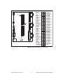
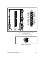
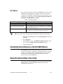
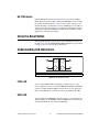
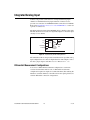
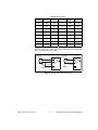
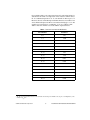
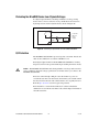
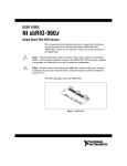
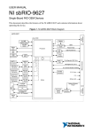
USER GUIDE NI sbRIO-961x/963x/964x and NI sbRIO-9612XT/9632XT/9642XT Single-Board RIO OEM Devices This document provides dimensions, pinouts, connectivity information, and specifications for the National Instruments sbRIO-9611, sbRIO-9612, sbRIO-9612XT, sbRIO-9631, sbRIO-9632, sbRIO-9632XT, sbRIO-9641, sbRIO-9642, and sbRIO-9642XT. The devices are referred to inclusively in this document as the NI sbRIO-961x/9612XT/963x/9632XT/964x/ 9642XT. Caution The NI sbRIO-961x/9612XT/963x/9632XT/964x/9642XT must be installed inside a suitable enclosure prior to use. Hazardous voltages may be present. National Instruments makes no product safety, electromagnetic compatibility (EMC), or CE marking compliance claims for NI sbRIO devices. The end-product supplier is responsible for conformity to any and all compliance requirements. Caution Caution Exercise caution when placing the NI sbRIO devices inside an enclosure. Auxiliary cooling may be necessary to keep the device under the maximum ambient temperature rating for the NI sbRIO device. Refer to Specifications section for more information about the maximum ambient temperature rating. Figure 1 shows the NI sbRIO-961x/9612XT/963x/9632XT and the NI sbRIO-964x/9642XT. NI sbRIO-961x/9612XT/963x/9632XT NI sbRIO-964x/9642XT Figure 1. NI sbRIO-961x/9612XT/963x/9632XT and NI sbRIO-964x/9642XT What You Need to Get Started This section lists the software and hardware you need to start programming the NI sbRIO device. Software Requirements You need a development computer with the following software installed on it. Go to ni.com/info and enter the Info Code rdsoftwareversion for information about software version compatibility. ❑ LabVIEW ❑ LabVIEW Real-Time Module ❑ LabVIEW FPGA Module ❑ NI-RIO Hardware Requirements You need the following hardware to use the NI sbRIO device. ❑ NI sbRIO-961x/9612XT/963x/9632XT/964x/9642XT ❑ 19–30 VDC power supply ❑ Ethernet cable NI sbRIO-961x/9612XT/963x/9632XT/964x/9642XT 2 ni.com Dimensions This section contains dimensional drawings of the NI sbRIO devices. For three-dimensional models, refer to the Resources tab of the NI sbRIO product page at ni.com. The plated mounting holes are all connected to P1, the ground lug. Connect P1 or one of the plated mounting holes securely to earth ground. Refer to the Understanding Ground Connections section for cautions about current loops through the grounding lug. Note Figure 2 shows the dimensions of the NI sbRIO-961x/9612XT/963x/ 9632XT/964x/9642XT. © National Instruments Corporation 3 NI sbRIO-961x/9612XT/963x/9632XT/964x/9642XT 8.200 (208.28) 8.076 (205.13) 5.826 (147.98) 5.121 (130.07) 4.466 (113.44) 2.916 (74.07) 1.556 (39.52) 5.550 (140.97) 5.415 (137.54) 12×Ø 0.134 (3.40) 4.400 (111.76) 2.440 (61.98) 2 mm Clearance Required Above This Capacitor 0.275 (6.99) 0.450 (11.43) 0.125 (3.18) 7.295 (185.29) 6.796 (172.62) 7.911 (200.94) 6.927 (175.95) 5.001 (127.03) 3.691 (93.75) 4.017 (102.03) 2.091 (53.11) 1.107 (28.12) 4.100 (104.14) 0.131 (3.33) 0.000 (0) 0.000 (0.00) 0.000 (0) 2 mm Clearance Required Above This Capacitor 0.651 (16.54) 0.574 (14.58) Ø 0.138 (3.50) 6-32 Threads Ø 0.112 (2.84) 6.617 (168.06) 5.633 (143.07) 0.327 (8.31) 0.000 (0) –0.110 (2.79) Minimum Clearance Needed Below Board 4-40 Threads 0.625 (15.88) 0.380 (9.65) 0.365 (9.28) 0.220 (5.59) 0.180 (4.57) 0.080 (2.03) 0.000 (0) 0.469 (11.91) 0.327 (8.31) 8.138 (206.71) 7.503 (190.58) 5.492 (139.5) 4.838 (122.89) 4.659 (118.33) 4.100 (104.14) 2.905 (73.79) 3.100 (78.74) 0.847 (21.52) 0.166 (4.22) 0.000 (0) 0.242 (6.16) Figure 2. NI sbRIO-961x/9612XT/963x/9632XT/964x/9642XT Dimensions in Inches (Millimeters) NI sbRIO-961x/9612XT/963x/9632XT/964x/9642XT 4 ni.com 8.709 (221.21) 2.889 (73.38) 2.910 (73.91) 5.799 (147.29) 5.820 (147.83) You can install up to three board-only C Series I/O modules on the NI sbRIO device. The following figure shows the dimensions of the NI sbRIO device with three board-only C Series I/O modules installed. 8.460 (214.88) 7.410 (188.21) 8×Ø 0.125 (3.18) 6.160 (156.46) 5.860 (148.84) 5.550 (140.97) 4.785 (121.55) 4.685 (119.00) 4.591 (116.60) 2.885 (73.28) 2.514 (63.86) 2 mm Clearance Required Above This Capacitor Ø 0.512 (13.00) 0.747 (18.97) 8.200 (208.28) 7.641 (194.08) 6.442 (163.63) 4.859 (123.42) 3.340 (84.84) 0.000 (0) 0.226 (5.74) 0.285 (7.24) 0.000 (0) Figure 3. NI sbRIO-961x/9612XT/963x/9632XT/964x/9642XT with C Series Modules, Dimensions in Inches (Millimeters) To maintain isolation clearances on the C Series modules, do not use mounting hardware larger than 0.240 in. (6.1 mm) in diameter and maintain an air gap of at least 0.200 in. (5.0 mm) from the modules to anything else. Note © National Instruments Corporation 5 NI sbRIO-961x/9612XT/963x/9632XT/964x/9642XT I/O and Other Connectors on the NI sbRIO Device Figure 4 shows the locations of parts on the NI sbRIO device. 1 2 3 2 4 2 5 6 2 7 2 2 8 19 2 9 18 2 2 10 2 17 1 2 3 4 5 6 7 8 9 10 16 2 15 J10, Connector for C Series Module 3 Plated Mounting Holes J7, Analog I/O Connector J9, Connector for C Series Module 2 J6, 24 V Digital Input (sbRIO-964x/9642XT Only) J8, Connector for C Series Module 1 J5, 24 V Digital Output (sbRIO-964x/9642XT Only) P4, 3.3 V Digital I/O Backup Battery P2, 3.3 V Digital I/O 14 13 12 11 12 13 14 15 16 17 18 19 2 11 J2, RJ-45 Ethernet Port J1, RS-232 Serial Port DIP Switches Reset Button P1, Ground Lug LEDs J3, Power Connector P3, 3.3 V Digital I/O P5, 3.3 V Digital I/O Figure 4. NI sbRIO Device Parts Locator Diagram NI sbRIO-961x/9612XT/963x/9632XT/964x/9642XT 6 ni.com Table 1 lists and describes the connectors on NI sbRIO devices and lists the part number and manufacturer of each connector. Refer to the manufacturer for information about using and matching these connectors. Table 1. NI sbRIO Connector Descriptions Manufacturer and Part Number Recommended Mating Connector 2-position MINI-COMBICON header and plug, 0.285 in. (7.24 mm) high Phoenix Contact, 1727566 Sauro, CTF02BV8-BN (included) J1, RS-232 Serial Port 9-pin DSUB plug, 0.318 in. (8.08 mm) high, with 4-40 jacksockets Tyco Electronics, 5747840-6 — P2, P3, P4, P5, J7 50-pin polarized header plug, 0.100 × 0.100 in. (2.54 × 2.54 mm) 3M, N2550-6002RB 3M, 8550-4500PL* J5 37-pin DSUB plug with 4-40 jacksockets FCI, D37P24B6GV00LF FCI, D37S24B6GV00 J6 34-pin polarized header plug, 0.100 × 0.100 in. (2.54 × 2.54 mm) 3M, N2534-6002RB 3M, 8534-4500PL† Connector Description J3, Power * (NI sbRIO-964x/9642XT Only) Use Samtec connector ESW-125-33-S-D if you are connecting one board to P2/P3/P4/P5/J7 and J5 to accommodate for the height of the J5 connector. † (NI sbRIO-964x/9642XT Only) Use Samtec connector ESW-117-33-S-D if you are connecting one board to J6 and J5 to accommodate for the height of the J5 connector. © National Instruments Corporation 7 NI sbRIO-961x/9612XT/963x/9632XT/964x/9642XT The following figures show the pinouts of the I/O connectors on the NI sbRIO devices. Pin 50 Pin 1 D GND 50 49 Port2/DIO8 D GND 48 47 Port2/DIO7 D GND 46 45 Port2/DIO6 D GND 44 43 Port2/DIO5 D GND 42 41 Port2/DIO4 D GND 40 39 Port6/DIO8 D GND 38 37 Port6/DIO7 D GND 36 35 Port6/DIO6 D GND 34 33 Port6/DIO5 D GND 32 31 Port6/DIO4 D GND 30 29 Port6/DIO3 D GND 28 27 Port6/DIO2 D GND 26 25 Port6/DIO1 D GND 24 23 Port6/DIO0 Port6/DIOCTL 22 21 Port6/DIO9 D GND 20 19 Port5/DIO8 D GND 18 17 Port5/DIO7 D GND 16 15 Port5/DIO6 D GND 14 13 Port5/DIO5 D GND 12 11 Port5/DIO4 5V 10 9 Port5/DIO3 D GND 8 7 Port5/DIO2 5V 6 5 Port5/DIO1 Port5/DIO9 4 3 Port5/DIO0 Port5/DIOCTL 2 1 D GND Figure 5. Pinout of I/O Connector P2, 3.3 V Digital I/O NI sbRIO-961x/9612XT/963x/9632XT/964x/9642XT 8 ni.com 50 49 48 47 Port9/DIO8 46 45 Port9/DIO6 5V D GND 44 43 42 41 Port9/DIO5 D GND 40 39 38 37 Port9/DIO3 36 35 34 33 Port9/DIO1 32 31 Port9/DIO9 Port8/DIO8 D GND 30 29 28 27 26 25 D GND D GND D GND D GND 24 22 20 18 23 21 19 17 Port8/DIO5 D GND D GND Port8/DIOCTL 16 15 14 13 12 11 Port8/DIO1 D GND D GND D GND 10 8 6 4 9 7 5 3 Port7/DIO8 2 1 D GND D GND 5V D GND Pin 50 D GND D GND D GND Port9/DIOCTL Pin 1 D GND D GND D GND Port7/DIO4 Port9/DIO7 Port9/DIO4 Port9/DIO2 Port9/DIO0 Port8/DIO7 Port8/DIO6 Port8/DIO4 Port8/DIO3 Port8/DIO2 Port8/DIO0 Port8/DIO9 Port7/DIO7 Port7/DIO6 Port7/DIO5 Figure 6. Pinout of I/O Connector P3, 3.3 V Digital I/O © National Instruments Corporation 9 NI sbRIO-961x/9612XT/963x/9632XT/964x/9642XT 50 49 48 47 Port2/DIO3 46 45 Port2/DIO1 D GND Port2/DIOCTL 44 43 42 41 Port2/DIO0 D GND 40 39 38 37 Port1/DIO8 36 35 34 33 Port1/DIO6 32 31 Port1/DIO4 Port1/DIO3 D GND 30 29 28 27 26 25 D GND Port1/DIOCTL D GND D GND 24 22 20 18 23 21 19 17 Port1/DIO0 D GND D GND D GND 16 15 14 13 12 11 Port0/DIO6 5V D GND 5V 10 8 6 4 9 7 5 3 Port0/DIO3 2 1 D GND D GND D GND D GND D GND D GND D GND D GND D GND D GND Pin 50 Pin 1 Port0/DIO9 Port0/DIOCTL Port2/DIO2 Port2/DIO9 Port1/DIO7 Port1/DIO5 Port1/DIO2 Port1/DIO1 Port1/DIO9 Port0/DIO8 Port0/DIO7 Port0/DIO5 Port0/DIO4 Port0/DIO2 Port0/DIO1 Port0/DIO0 Figure 7. Pinout of I/O Connector P4, 3.3 V Digital I/O NI sbRIO-961x/9612XT/963x/9632XT/964x/9642XT 10 ni.com 50 49 48 47 Port4/DIO8 46 45 Port4/DIO6 5V D GND 44 43 42 41 Port4/DIO5 D GND 40 39 38 37 Port4/DIO3 36 35 34 33 Port4/DIO1 31 Port4/DIO9 29 27 25 Port3/DIO8 23 21 19 17 Port3/DIO5 16 15 D GND 14 13 D GND Port3/DIOCTL 12 11 10 9 D GND 8 7 D GND 6 5 D GND 4 3 Port7/DIO9 Port3/DIO1 D GND 5V D GND Pin 50 D GND D GND D GND Port4/DIOCTL 32 30 D GND 28 D GND 26 D GND Pin 1 D GND D GND D GND D GND Port7/DIOCTL 24 22 20 18 2 1 Port4/DIO7 Port4/DIO4 Port4/DIO2 Port4/DIO0 Port3/DIO7 Port3/DIO6 Port3/DIO4 Port3/DIO3 Port3/DIO2 Port3/DIO0 Port3/DIO9 Port7/DIO3 Port7/DIO2 Port7/DIO1 Port7/DIO0 D GND Figure 8. Pinout of I/O Connector P5, 3.3 V Digital I/O © National Instruments Corporation 11 NI sbRIO-961x/9612XT/963x/9632XT/964x/9642XT Pin 1 AI GND 1 2 AI8 3 5 7 4 6 8 AI11 9 10 AI GND AI12 11 12 13 14 AI5 15 16 AI6 17 19 21 23 25 AI1 AI2 Pin 50 AI15 AI GND AI24 AI17 AI18 AI27 AI GND AI0 AI9 AI GND AI10 AI3 AI4 AI13 AI GND 18 20 22 24 26 AI14 AI7 27 28 29 30 31 32 AI26 AI19 AI16 AI25 AI GND 33 34 35 36 AI20 AI29 AI GND 37 38 39 40 AI30 AI23 AO3 41 42 43 44 AO2 45 46 AO GND AO GND AO GND AO1 47 48 49 50 AO GND AI GND AI28 AI21 AI22 AI31 AI SENSE AO0 Figure 9. Pinout of I/O Connector J7, Analog I/O NI sbRIO-961x/9612XT/963x/9632XT/964x/9642XT 12 ni.com Pin 34 Pin 1 D GND 34 33 DI31 DI30 32 31 DI29 DI28 30 29 DI27 DI26 28 27 DI25 DI24 26 25 DI23 DI22 24 23 DI21 DI20 22 21 DI19 DI18 20 19 DI17 DI16 18 17 DI15 DI14 16 15 DI13 DI12 14 13 DIa11 DI10 12 11 DI9 DI8 10 9 DI7 DI6 8 7 DI5 DI4 6 5 DI3 DI2 4 3 DI1 DI0 2 1 D GND Figure 10. Pinout of I/O Connector J6, 24 V Digital Input (NI sbRIO-964x/9642XT Only) © National Instruments Corporation 13 NI sbRIO-961x/9612XT/963x/9632XT/964x/9642XT D GND DO15 DO14 DO13 DO12 DO11 DO10 DO9 DO8 Vsup Vsup DO7 DO6 DO5 DO4 DO3 DO2 DO1 DO0 Pin 37 19 18 17 16 15 14 13 12 11 10 9 8 7 6 5 4 3 2 1 37 36 35 34 33 32 31 30 29 28 27 26 25 24 23 22 21 20 DO31 DO30 DO29 DO28 DO27 DO26 DO25 DO24 Vsup Vsup DO23 DO22 DO21 DO20 DO19 DO18 DO17 DO16 Pin 1 Figure 11. Pinout of I/O Connector J5, 24 V Digital Output (NI sbRIO-964x/9642XT Only) Figure 12 shows the signals on J1, the RS-232 serial port. DSR RTS CTS RI 1 6 2 7 3 8 4 9 5 DCD RXD TXD DTR GND Figure 12. J1, RS-232 Serial Port NI sbRIO-961x/9612XT/963x/9632XT/964x/9642XT 14 ni.com Understanding Ground Connections All of the grounds (D GND, AI GND, AO GND, ground lug P1, and the plated mounting holes) are connected together internally on the NI sbRIO device. The ESD protection diodes are connected to the plated mounting holes with a lower inductive path than the path to D GND, so the best ESD protection is provided by connecting the plated mounting holes and ground lug P1 to a low inductive earth ground. Care must be taken to not connect the grounds in such a way that stray power supply currents traverse through the board. For example, when using the NI sbRIO-964x/9642XT, the D GND connections on the 24 V DIO connectors J5 and J6 should not be carrying more than a few tens of milliamps of current. Ideally, only the return current for the 24 V inputs should return through D GND on J5, and D GND on J6 should have no current flow. For the remaining connectors, a good rule of thumb is current flowing out of the connector should match current flowing in. To verify correct grounding of the NI sbRIO device, make sure current flowing into the power connector J3 equals the current flowing out of power connector J3. These currents should be measured with a current probe after final assembly of the end product and any current differences investigated and removed. All external power supplies should have their connected to a system ground external to the NI sbRIO device. Do not use the NI sbRIO device as the common system grounding point. Significant currents traversing through the NI sbRIO grounds can result in digital component failures. If more than 3 A flows through the common (–) pin on the J3 power connector, components start to fuse open. Connecting the NI sbRIO Device to a Network Use a standard Category 5 (CAT-5) or better Ethernet cable to connect the RJ-45 Ethernet port to an Ethernet network. To prevent data loss and to maintain the integrity of your Ethernet installation, do not use a cable longer than 100 m. Caution If you need to build your own cable, refer to the Cabling section for more information about Ethernet cable wiring connections. © National Instruments Corporation 15 NI sbRIO-961x/9612XT/963x/9632XT/964x/9642XT The host computer communicates with the device over a standard Ethernet connection. If the host computer is on a network, you must configure the device on the same subnet as the host computer. If neither the host computer nor the device is connected to a network, you can connect the two directly using a crossover cable. If you want to use the device on a subnet other than the one the host computer is on, first connect the device on the same subnet as the host computer. Use DHCP to assign an IP address or reassign a static IP address for the subnet where you want it to be and physically move it to the other subnet. Refer to the Measurement & Automation Explorer Help for more information about configuring the device in Measurement & Automation Explorer (MAX). Powering the NI sbRIO Device The NI sbRIO device requires a power supply connected to J3. The supply voltage and current must meet the specifications in the Power Requirements section of this document, but the actual power requirement depends on how the device is physically configured, programmed, and used. To determine the power requirement of your application, you must measure the power consumption during execution, and add 20% to your estimates to account for transient and startup conditions. Select a high-quality power supply with less than 20 mV ripple. The NI sbRIO device has some internal power-supply filtering on the positive side, but a low-quality power supply can inject noise into the ground path, which is unfiltered. Note Four elements of the NI sbRIO device can require power: NI sbRIO internal operation, including integrated analog and digital I/O; 3.3 V DIO; 5 V output; and board-only C Series modules installed on the device. Refer to the Power Requirements section for formulas and examples for calculating power requirements for different configurations and application types. Complete the following steps to connect a power supply to the device. Refer to Figure 13 for an illustration of the power supply connection. NI sbRIO-961x/9612XT/963x/9632XT/964x/9642XT 16 ni.com V C Common (–) Voltage (+) Figure 13. Connecting a Power Supply 1. Remove the MINI-COMBICON plug from connector J3 of the NI sbRIO device. Refer to Figure 4 for the location of J3. 2. Connect the positive lead of the power supply to the V terminal of the MINI-COMBICON plug. 3. Connect the negative lead of the power supply to the C terminal of the MINI-COMBICON plug. 4. Re-install the MINI-COMBICON connector in connector J3. The 24 V digital output of the NI sbRIO-964x/9642XT requires a separate, additional power supply. Refer to the Integrated 24 V Digital Output (NI sbRIO-964x/9642XT Only) and Specifications sections for more information about powering digital output channels. Note Powering On the NI sbRIO Device When you apply power to the NI sbRIO device, the device runs a power-on self test (POST). During the POST, the Power and Status LEDs turn on. When the Status LED turns off, the POST is complete. If the LEDs do not behave in this way when the system powers on, refer to the Understanding LED Indications section. You can configure the device to launch an embedded stand-alone LabVIEW RT application each time it is booted. Refer to the Running a Stand-Alone Real-Time Application (RT Module) topic of the LabVIEW Help for more information. © National Instruments Corporation 17 NI sbRIO-961x/9612XT/963x/9632XT/964x/9642XT Boot Options Table 2 lists the reset options available on NI sbRIO devices. These options determine how the FPGA behaves when the device is reset in various conditions. Use the RIO Device Setup utility to select reset options. Access the RIO Device Setup utility by selecting Start»All Programs»National Instruments»NI-RIO»RIO Device Setup. Table 2. NI sbRIO Reset Options Reset Option Behavior Do not autoload VI Does not load the FPGA bit stream from flash memory. Autoload VI on device powerup Loads the FPGA bit stream from flash memory to the FPGA when the device powers on. Autoload VI on device reboot Loads the FPGA bit stream from flash to the FPGA when you reboot the device either with or without cycling power. Note If you want a VI to run when loaded to the FPGA, complete the following steps. 1. Right-click the FPGA Target item in the Project Explorer window in LabVIEW. 2. Select Properties. 3. In the General category of the FPGA Target Properties dialog box, place a check in the Run when loaded to FPGA checkbox. 4. Compile the FPGA VI. Connecting Serial Devices to the NI sbRIO Device The NI sbRIO device has an RS-232 serial port to which you can connect devices such as displays or input devices. Use the Serial VIs to read from and write to the serial port from a LabVIEW RT application. For more information about using the Serial VIs, refer to the Serial VIs and Functions topic of the LabVIEW Help. Using the Internal Real-Time Clock The system clock of the NI sbRIO device gets the date and time from the internal real-time clock at startup. This synchronization provides timestamp data to the device. NI sbRIO-961x/9612XT/963x/9632XT/964x/9642XT 18 ni.com Configuring DIP Switches AMP 0650 1-5435802-7 OFF 1 2 SAFE MODE CONSOLE OUT 3 4 IP RESET NO APP 5 6 USER1 NO FPGA Figure 14. DIP Switches All of the DIP switches are in the OFF (up) position when the NI sbRIO device is shipped from National Instruments. SAFE MODE Switch The position of the SAFE MODE switch determines whether the embedded LabVIEW Real-Time engine launches at startup. If the switch is in the OFF position, the LabVIEW Real-Time engine launches. Keep this switch in the OFF position during normal operation. If the switch is in the ON position at startup, the NI sbRIO device launches only the essential services required for updating its configuration and installing software. The LabVIEW Real-Time engine does not launch. Push the SAFE MODE switch to the ON position if the software on the NI sbRIO device is corrupted. Even if the switch is not in the ON position, if there is no software installed on the device, the device automatically boots into safe mode. The SAFE MODE switch must be in the ON position to reformat the drive on the device. Refer to the Measurement & Automation Explorer Help for more about installing software and reformatting the drive. © National Instruments Corporation 19 NI sbRIO-961x/9612XT/963x/9632XT/964x/9642XT CONSOLE OUT Switch With a serial-port terminal program, you can use the serial port to read the IP address and firmware version of the NI sbRIO device. Use a null-modem cable to connect the serial port on the device to a computer. Push the CONSOLE OUT switch to the ON position. Make sure that the serial-port terminal program is configured to the following settings: • 9,600 bits per second • Eight data bits • No parity • One stop bit • No flow control Keep this switch in the OFF position during normal operation. If CONSOLE OUT is enabled, LabVIEW RT cannot communicate with the serial port. IP RESET Switch Push the IP RESET switch to the ON position and reboot the NI sbRIO device to reset the IP address to 0.0.0.0. If the device is on your local subnet and the IP RESET switch is in the ON position, the device appears in MAX with IP address 0.0.0.0. You can configure a new IP address for the device in MAX. Refer to the Resetting the Network Configuration of the NI sbRIO Device section for more information about resetting the IP address. NO APP Switch Push the NO APP switch to the ON position to prevent a LabVIEW RT startup application from running at startup. If you want to permanently disable a LabVIEW RT application from running at startup, you must disable it in LabVIEW. To run an application at startup, push the NO APP switch to the OFF position, create an application using the LabVIEW Application Builder, and configure the application in LabVIEW to launch at startup. For more information about automatically launching VIs at startup and disabling VIs from launching at startup, refer to the Running a Stand-Alone Real-Time Application (RT Module) topic of the LabVIEW Help. USER1 Switch You can define the USER1 switch for your application. To define the purpose of this switch in your embedded application, use the RT Read Switch VI in your LabVIEW RT embedded VI. For more information about the RT Read Switch VI, refer to the LabVIEW Help. NI sbRIO-961x/9612XT/963x/9632XT/964x/9642XT 20 ni.com NO FPGA Switch Push the NO FPGA switch to the ON position to prevent a LabVIEW FPGA application from loading at startup. The NO FPGA switch overrides the options described in the Boot Options section. After startup you can download bit files to flash memory from a LabVIEW project regardless of switch position. If you already have an application configured to launch at startup and you push the NO FPGA switch from ON to OFF, the startup application is automatically enabled. Using the Reset Button Pressing the Reset button reboots the processor. The FPGA continues to run unless you select the Autoload VI on device reboot boot option. Refer to the Boot Options section for more information. Understanding LED Indications 1 FPGA 1 3 2 4 2 USER 3 POWER 4 STATUS Figure 15. NI sbRIO Device LEDs FPGA LED You can use the FPGA LED to help debug your application or easily retrieve application status. Use the LabVIEW FPGA Module and NI-RIO software to define the FPGA LED to meet the needs of your application. Refer to LabVIEW Help for information about programming this LED. USER LED You can define the USER LED to meet the needs of your application. To define the LED, use the RT LEDs VI in LabVIEW. For more information about the RT LEDs VI, refer to the LabVIEW Help. © National Instruments Corporation 21 NI sbRIO-961x/9612XT/963x/9632XT/964x/9642XT POWER LED The POWER LED is lit while the NI sbRIO device is powered on. This LED indicates that the 5 V and 3.3 V rails are stable. STATUS LED The STATUS LED is off during normal operation. The NI sbRIO device indicates specific error conditions by flashing the STATUS LED a certain number of times as shown in Table 3. Table 3. Status LED Indications Number of Flashes Indication 1 (one flash every couple seconds) The device is unconfigured. Use MAX to configure the device. Refer to the Measurement & Automation Explorer Help for information about configuring the device. 2 The device has detected an error in its software. This usually occurs when an attempt to upgrade the software is interrupted. Reinstall software on the device. Refer to the Measurement & Automation Explorer Help for information about installing software on the device. 3 The device is in safe mode because the SAFE MODE DIP switch is in the ON position. Refer to the Configuring DIP Switches section for information about the SAFE MODE DIP switch. 4 The device software has crashed twice without rebooting or cycling power between crashes. This usually occurs when the device runs out of memory. Review your RT VI and check the device memory usage. Modify the VI as necessary to solve the memory usage issue. Continuous flashing or solid The device has detected an unrecoverable error. Format the hard drive on the device. If the problem persists, contact National Instruments. NI sbRIO-961x/9612XT/963x/9632XT/964x/9642XT 22 ni.com Resetting the Network Configuration of the NI sbRIO Device If the NI sbRIO device is not able to communicate with the network, you can use the IP RESET switch to manually restore the device to the factory network settings. When you restore the device to the factory network settings, the IP address, subnet mask, DNS address, gateway, and Time Server IP are set to 0.0.0.0. Power-on defaults, watchdog settings, and VIs are unaffected. Complete the following steps to restore the device to the factory network settings. 1. Move the IP RESET DIP switch to the ON position. 2. Press the Reset button. 3. Move the IP RESET switch to the OFF position. The network settings are restored. You can reconfigure the settings in MAX from a computer on the same subnet. Refer to the Measurement & Automation Explorer Help for more information about configuring the device. Note If the device is restored to the factory network settings, the LabVIEW run-time engine does not load. You must reconfigure the network settings and reboot the device for the LabVIEW run-time engine to load. © National Instruments Corporation 23 NI sbRIO-961x/9612XT/963x/9632XT/964x/9642XT Integrated 3.3 V Digital I/O The four 50-pin IDC headers, P2–P5, provide connections for 110 low-voltage DIO channels, 82 D GND, and eight +5 V voltage outputs. Figure 16 represents a single DIO channel. +5 V D1 R1 Xilinx Spartan-3 FPGA User Connection U1 D2 U1: 5 V to 3.3 V Level Shifter, SN74CBTD3384CDGV from Texas Instruments D1 and D2: ESD-Rated Protection Diodes, NUP4302MR6T1G from ON Semiconductor R1: Current-Limiting Posistor, PRG18BB330MS1RB from Murata Figure 16. Circuitry of One 3.3 V DIO Channel I/O Protection The 33 Ω current-limiting posistor, R1, and the protection diodes, D1 and D2, protect each DIO channel against externally applied voltages and ESD events. The combination of R1 and D1 protects against overvoltage, and the combination of R1 and D2 protects against undervoltage. The resistance of R1 increases rapidly with temperature. During overvoltage conditions, high current flows through R1 and into the protection diodes. High current causes internal heating in the posistor, which increases the resistance and limits the current. Refer to the Specifications section for current-limiting and resistance values. Drive Strength The NI sbRIO devices are tested with all 110 DIO channels driving 3 mA DC loads, for a total of 330 mA sourcing from the FPGA. The FPGA uses minimum 8 mA drivers, but the devices are not characterized for loads higher than 3 mA. NI sbRIO-961x/9612XT/963x/9632XT/964x/9642XT 24 ni.com Signal Integrity NI sbRIO boards have a 60 Ω characteristic trace impedance. The characteristic impedance of most IDC ribbon cables is 110 Ω, which is grossly mismatched from the board. However, headers P2–P5 were designed such that the signals are interwoven with ground (signal/ground/signal/ground, etc.), which greatly improves the signal integrity. This is sufficient for most applications For the best possible signal integrity, use a 3M 3353 series ribbon cable, which has a characteristic impedance of 65 Ω. This cable has a ground plane that connects to the ground plane of the board at pin 1 and pin 50. The internal ground plane of this cable also reduces noise and radiated emissions. Using +5 V Power from 3.3 V DIO Headers P2–P5 Each of the four DIO headers has two pins to provide +5 V power for external applications. These +5 V outputs are referenced to D GND on the headers and are connected directly to the internal 5 V power plane of the NI sbRIO device. The +5 V source has current limiting and overvoltage clamps. Nevertheless, sudden current steps and noisy loads can inject high-frequency transients into the power planes of the device. Such transients can cause intermittent failures in the digital timing and lead to unexpected behavior. Add filters and/or additional current limiting between the external load and the +5 V output if the external load is not a quiet, slowly ramping DC load. An LC filter of 6.8 μH and 100 μF per 200 mA load should be sufficient, but the OEM user is responsible for final requirements and testing. The NI sbRIO power supply has a total of 2 A external load at 5 V. This total includes 200 mA per installed C Series module. For example, if three C Series modules are installed, only 2 A – (3 × 0.2) = 1.4 A is available for use on headers P2–P5. Each pin on the headers is rated for 2 A, but a typical 28 AWG ribbon cable is rated for only 225 mA per conductor. The OEM user is responsible for determining cabling requirements and ensuring that current limits are not exceeded. © National Instruments Corporation 25 NI sbRIO-961x/9612XT/963x/9632XT/964x/9642XT Integrated Analog Input Connector J7 provides connections for 32 single-ended analog input channels or 16 differential analog input channels. Connector J7 also provides one connection for AI SENSE and nine connections for AI GND. Refer to the I/O and Other Connectors on the NI sbRIO Device section for a pinout of connector J7. The integrated analog input of the NI sbRIO device is similar to that of the NI 9205, but there is no isolation or digital I/O. Figure 17 shows the input circuitry for one channel. Trigger AI+ AI– MUX PGIA AISENSE AI GND Filtered Differential Amplifier Trig ADC 16-bit ADC Figure 17. Input Circuitry for One Analog Channel The remainder of this section provides a brief discussion of possible analog input configurations. For a more in-depth discussion and examples, refer to the Analog Input chapter of the M Series User Manual on ni.com. Differential Measurement Configurations You can use a differential measurement configuration to attain more accurate measurements and less noise. A differential measurement configuration requires two inputs for each measurement, thus reducing the number of available channels to 16. Table 4 shows the signal pairs that are valid for differential connection configurations. NI sbRIO-961x/9612XT/963x/9632XT/964x/9642XT 26 ni.com Table 4. Differential Pairs Channel Signal+ Signal– Channel Signal+ Signal– 0 AI0 AI8 16 AI16 AI24 1 AI1 AI9 17 AI17 AI25 2 AI2 AI10 18 AI18 AI26 3 AI3 AI11 19 AI19 AI27 4 AI4 AI12 20 AI20 AI28 5 AI5 AI13 21 AI21 AI29 6 AI6 AI14 22 AI22 AI30 7 AI7 AI15 23 AI23 AI31 Figure 18 shows how to make a differential connection for a floating signal and for a ground-referenced signal. Floating Signal Source AI+ + – AI– Rb Rb AI GND Grounded Signal Source + – AI+ + – AI– + – AI GND Rb = 100 kΩ –1 MΩ Figure 18. Differential Analog Input Connection © National Instruments Corporation 27 NI sbRIO-961x/9612XT/963x/9632XT/964x/9642XT Referenced Single-Ended (RSE) Measurements You can use an RSE measurement configuration to take measurements on 32 channels when all channels share a common ground. Figure 19 shows how to make an RSE analog input connection for a floating signal. National Instruments does not recommend making an RSE connection for a ground-referenced signal. NOT RECOMMENDED Floating Signal Source Grounded Signal Source AI AI + + – + + – – – VA AI GND VB AI GND Ground-loop potential (VA – VB) is added to measured signal. Figure 19. RSE Analog Input Connection In an RSE connection configuration, the NI sbRIO device measures each input channel with respect to AI GND. Non-Referenced, Single-Ended (NRSE) Measurements You can use an NRSE measurement configuration to take measurements on all 32 channels while reducing noise more effectively than with an RSE connection configuration. This configuration provides remote sense for the negative (–) input of the programmable gain instrumentation amplifier (PGIA) that is shared by all channels configured for NRSE mode. The behavior of this configuration is similar to the behavior of RSE connections, but it provides improved noise rejection. Figure 20 shows how to make an NRSE analog input connection for a floating signal and for a ground-referenced signal. Floating Signal Source Grounded Signal Source AI + – + – Rb AI + – + – AI SENSE AI SENSE AI GND AI GND Rb = 100 kΩ –1 MΩ Figure 20. NRSE Analog Input Connection NI sbRIO-961x/9612XT/963x/9632XT/964x/9642XT 28 ni.com The analog input and analog output of the NI sbRIO-963x/9632XT/964x/9642XT share an internal power supply. Putting the analog input into Sleep Mode turns off analog output as well. However, putting analog output into Sleep Mode does not turn off analog input. Note Integrated Analog Output (NI sbRIO-963x/9632XT/964x/9642XT Only) Connector J7 of the NI sbRIO-963x/9632XT/964x/9642XT provides connections for four analog output channels. Refer to the I/O and Other Connectors on the NI sbRIO Device section for a pinout of connector J7. The integrated analog output of the NI sbRIO device is similar to that of the NI 9263, but there is no isolation. Each channel has a digital-to-analog converter that produces a voltage signal. Each channel also has overvoltage and short-circuit protection. Refer to the Specifications section for information about the overvoltage and short-circuit protection. Figure 21 shows the analog output circuitry for one channel. Overvoltage/ Short-Circuit Protection DAC Amplifier AO AO GND Figure 21. Analog Output Circuitry for One Channel When you apply power to the NI sbRIO device, analog output channels are unpowered until data is written to them. When the channels receive the first data, they turn on and drive the output voltage configured in software. This behavior is similar to that of the NI 9263. Refer to the Specifications section for more information about power-on voltage. Refer to the software help for information about configuring startup output states in software. © National Instruments Corporation 29 NI sbRIO-961x/9612XT/963x/9632XT/964x/9642XT Connect the positive lead of the load to the AO terminal. Connect the ground of the load to an AO GND terminal. Figure 22 shows a load connected to one analog input channel. AO Load AO GND Figure 22. Load Connected to One Analog Input Channel Integrated 24 V Digital Input (NI sbRIO-964x/9642XT Only) Connector J6 of the NI sbRIO-964x/9642XT provides connections for 32 simultaneously sampled digital input channels. Each channel has one pin, DI, to which you can connect a digital input signal. The remaining two pins of J6 are the ground reference pins, D GND. Refer to the I/O and Other Connectors on the NI sbRIO Device section for a pinout of connector J6. The integrated digital input of the NI sbRIO device is similar to that of the NI 9425, but there is no isolation. The 24 V digital input channels are sinking inputs, meaning that when the device drives a current or applies a voltage to the DI pin, the pin provides a path to D GND. D GND is the current return path for sourcing digital input devices. The NI sbRIO-964x/ 9642XT internally limits current signals connected to DI. For more information about input current protection, refer to the Specifications section. You can connect 2-, 3-, and 4-wire sourcing-output devices to the NI sbRIO-964x/9642XT. A sourcing-output device drives current or applies voltage to the DI pin. An example of a sourcing-output device is an open collector PNP. NI sbRIO-961x/9612XT/963x/9632XT/964x/9642XT 30 ni.com Connect the sourcing-output device to the DI pin on the NI sbRIO-9642/ 9642XT. Connect the common of the external device to the D GND pin. Refer to Figure 23 for an illustration of connecting a device to the NI sbRIO-9642/9642XT. Sourcing-Output Device DI External + Power Supply _ D GND Figure 23. Device Connected to One Digital Input Channel The digital input channel registers as ON when the sourcing-output device applies a voltage or drives a current to the DI pin that is in the input ON range. The channel registers as OFF when the device applies a voltage or drives a current to the DI pin that is in the input OFF range. If no device is connected to the DI pin, the channel registers as OFF. Refer to the Specifications section for more information about ON and OFF states. Integrated 24 V Digital Output (NI sbRIO-964x/9642XT Only) Connector J5 of the NI sbRIO-964x/9642XT provides connections for 32 current-sourcing digital output channels. Refer to the I/O and Other Connectors on the NI sbRIO Device section for a pinout of connector J5. The DO pin of the channel drives current or applies voltage to a connected device. You can directly connect the NI sbRIO-964x/9642XT to a variety of industrial devices such as motors, actuators, relays, and lamps. Make sure the devices you connect to the NI sbRIO-964x/9642XT are compatible with the output specifications. Refer to the Specifications section for the output specifications. The 24 V digital outputs of the NI sbRIO-964x/9642XT require a 6–35 VDC power supply separate from the power supply connected to J3. © National Instruments Corporation 31 NI sbRIO-961x/9612XT/963x/9632XT/964x/9642XT Connect the device to DO and D GND, and connect the external power supply to Vsup and D GND, as shown in Figure 24. Vsup DO Device D GND 6–35 VDC + External Power – Supply Figure 24. Device Connected to One Digital Output Channel Increasing Current Drive If you do not modify the NI sbRIO device, each channel has a continuous output current of 250 mA. If you want to increase the output current to a device, you can connect any number of channels together in parallel. For example, if you want to drive 1 A of current, connect DO<0..3> in parallel as shown in Figure 25. You must turn all parallel channels on and off simultaneously so that the current on any single channel cannot exceed the 250 mA rating. You must also select heavier cabling for the connection between the negative terminal of the device and the negative terminal of the power supply for the device. Refer to Figure 25 and use heavier cabling where indicated by heavier traces. Vsup 250 mA 1A 6–35 VDC + External Power – Supply DO0 250 mA DO1 250 mA DO2 + Device – 250 mA DO3 D GND Figure 25. Increasing the Current to a Device Note Refer to the Understanding Ground Connections section for cautions about D GND. NI sbRIO-961x/9612XT/963x/9632XT/964x/9642XT 32 ni.com If you add heat sinks to the output transistors U49–U56 and U110–U117, such that the measured case temperature of the transistors remains below 65 °C at ambient temperature of 55 °C, each channel can drive up to 1.5 A. However, the total current through all channels must not exceed 20 A.1 Use a heat sink that dissipates 0.5 W for each transistor driving up to 1.5 A. For example, for four transistors, each driving 1.5 A, use a 2 W heat sink. Table 5 shows the channels associated with the output transistors. Table 5. Transistors Associated with DO Channels 1 DO Channels Transistor 0, 1 U49 2, 3 U50 4, 5 U51 6, 7 U52 8, 9 U53 10, 11 U54 12, 13 U55 14, 15 U56 16, 17 U117 18, 19 U116 20, 21 U115 22, 23 U114 24, 25 U113 26, 27 U112 28, 29 U111 30, 31 U110 The 20 A total-current limit is based on the maximum current rating of the DSUB connector pins, 5 A, multiplied by 4, the number of Vsup pins. © National Instruments Corporation 33 NI sbRIO-961x/9612XT/963x/9632XT/964x/9642XT Protecting the NI sbRIO Device from Flyback Voltages If a digital output channel is switching an inductive or energy-storing device such as a motor, solenoid, or relay, and the device does not have flyback protection, install a flyback diode as shown in Figure 26. Vsup D GND 6–35 VDC External Power – Supply + DO Flyback Inductive Diode Device Figure 26. Connecting a Flyback Diode to the NI sbRIO 964x/9642XT I/O Protection The NI sbRIO-964x/9642XT is protected against overcurrent, inrush, and short-circuit conditions in accordance with IEC 1131-2. Each digital output channel on the NI sbRIO-964x/9642XT has circuitry that protects it from voltage and current surges resulting from short circuits. The NI sbRIO-964x/9642XT can be damaged under overvoltage and reverse bias voltage conditions. Check the voltage specifications for all devices that you connect to the NI sbRIO-964x/9642XT. Caution Excessive current through a DO pin causes the channel to go into an overcurrent state. In an overcurrent state, the channel cycles off and on until the short circuit is removed or the current returns to an acceptably low level. Refer the Specifications section for typical trip currents. Each channel has a status line that indicates in software whether the channel is in an overcurrent state. Refer to the software help for information about the status line. NI sbRIO-961x/9612XT/963x/9632XT/964x/9642XT 34 ni.com Specifications Unless otherwise noted, the following specifications are typical for the range –40 to 85 °C for the NI sbRIO-96x2XT, and for the range –20 to 55 °C for the NI sbRIO-961x/963x/964x. Network Network interface................................... 10BaseT and 100BaseTX Ethernet Compatibility ......................................... IEEE 802.3 Communication rates ............................. 10 Mbps, 100 Mbps, auto-negotiated Maximum cabling distance .................... 100 m/segment RS-232 DTE Serial Port Baud rate support ................................... Arbitrary Maximum baud rate ............................... 115,200 bps Data bits ................................................. 5, 6, 7, 8 Stop bits.................................................. 1, 2 Parity ...................................................... Odd, Even, Mark, Space, None Flow control ........................................... RTS/CTS, XON/XOFF, DTR/DSR, None Processor Speed NI sbRIO-9611/9631/9641 .................... 266 MHz NI sbRIO-9612/9632/9642 and NI sbRIO-96x2XT.................................. 400 MHz © National Instruments Corporation 35 NI sbRIO-961x/9612XT/963x/9632XT/964x/9642XT Memory Nonvolatile memory NI sbRIO-9611/9631/9641..............128 MB minimum NI sbRIO-9612/9632/9642 and NI sbRIO-96x2XT ...........................256 MB minimum System memory NI sbRIO-9611/9631/9641..............64 MB minimum NI sbRIO-9612/9632/9642 and NI sbRIO-96x2XT ...........................128 MB minimum For information about the life span of the nonvolatile memory and about best practices for using nonvolatile memory, go to ni.com/info and enter the Info Code SSDBP. Xilinx Spartan-3 Reconfigurable FPGA Number of logic cells NI sbRIO-9611/9631/9641..............17,280 NI sbRIO-9612/9632/9642 and NI sbRIO-96x2XT ...........................46,080 Available embedded RAM NI sbRIO-9611/9631/9641..............432 kbits NI sbRIO-9612/9632/9642 and NI sbRIO-96x2XT ...........................720 kbits 3.3 V Digital I/O Number of DIO channels........................110 Maximum tested current per channel .....3 mA Maximum total current, all lines.............330 mA Maximum tested DIO frequency ............10 MHz Input logic levels Input high voltage, VIH ....................2.0 V min; 5.25 V max Input low voltage, VIL ......................0 V min; 0.8 V max NI sbRIO-961x/9612XT/963x/9632XT/964x/9642XT 36 ni.com Output logic levels Output high voltage, VOH , sourcing 3 mA................................. 2.7 V min; 3.3 V max Output low voltage, VOL , sinking 3 mA................................... 0.07 V min; 0.54 V max Overvoltage protection (maximum 2 pins in overvoltage) NI sbRIO-961x/963x/964x at –20 to 55 °C ......................... ±20 V NI sbRIO-96x2XT at –20 to 85 °C ......................... ±20 V at –40 to –20 °C ....................... ±7 V Posistor (PRG18BB330MS1RB from Murata) Maximum peak abnormal-condition current............. 760 mA Maximum hold current at 25 °C ..... 36 mA Maximum hold current at 70 °C ..... 20 mA Maximum hold current at 85 °C (NI sbRIO-96x2XT only)................ 3 mA Trip current at 25 °C ....................... 71 mA Resistance at 25 °C ......................... 33 Ω ±20% © National Instruments Corporation 37 NI sbRIO-961x/9612XT/963x/9632XT/964x/9642XT Resistance-temperature characteristics, typical curve Resistance-Temperature Characteristics Typical Curve 1000 Resistance Change (R/R25) 100 10 1 0.1 –40 –20 0 20 40 60 80 100 120 140 160 Temperature (°C) NI sbRIO-961x/9612XT/963x/9632XT/964x/9642XT 38 ni.com Analog Input All voltages are relative to AI GND unless otherwise noted. Number of channels ............................... 32 single-ended or 16 differential analog input channels ADC resolution ...................................... 16 bits Differential nonlinearity......................... No missing codes guaranteed Integrated nonlinearity ........................... Refer to the AI Absolute Accuracy Tables and Formulas Conversion time ..................................... 4.00 μs (250 kS/s) Input coupling ........................................ DC Nominal input ranges ............................. ±10 V, ±5 V, ±1 V, ±0.2 V Minimum overrange (for 10 V range)...................................... 4% Maximum working voltage for analog inputs (signal + common mode) ....................... Each channel must remain within ±10.4 V of common Input impedance (AI-to-AI GND) Powered on ..................................... >10 GΩ in parallel with 100 pF Powered off/overload...................... 1.2 kΩ min Input bias current ................................... ±100 pA Crosstalk (at 100 kHz) Adjacent channels ........................... –65 dB Non-adjacent channels .................... –70 dB Small-signal bandwidth.......................... 700 kHz Overvoltage protection AI channel (0 to 31) ........................ ±24 V (one channel only) AISENSE ........................................ ±24 V CMRR (DC to 60 Hz) ............................ 92 dB © National Instruments Corporation 39 NI sbRIO-961x/9612XT/963x/9632XT/964x/9642XT Typical performance graphs Settling Error Versus Time for Different Source Impedances Error (ppm of Step Size) 10 k 10 kΩ 5 kΩ 1k 2 kΩ 100 1 kΩ ≤100 Ω 10 1 1 10 Time (μs) 100 Normalized Signal Amplitude (dB) AI <0..31> Small Signal Bandwidth 2 0 –2 –4 –6 –8 –10 –12 –14 1k 10 k 100 k 1000 k Frequency (Hz) 10000 k AI <0..31> CMRR 120 0.2 V Range CMRR (dB) 100 1 V Range 80 10 V Range 60 5 V Range 40 20 0 10 NI sbRIO-961x/9612XT/963x/9632XT/964x/9642XT 100 40 1k 10 k Frequency (Hz) 100 k ni.com Settling time for multichannel measurements, accuracy, all ranges ±120 ppm of full-scale step (±8 LSB) ......................................... 4 μs convert interval, 5.5 μs (from 50 to 85 °C) ±30 ppm of full-scale step (±2 LSB) ......................................... 8 μs convert interval Analog triggers Number of triggers.......................... 1 Resolution ....................................... 10 bits, 1 in 1,024 Bandwidth (–3 dB).......................... 700 kHz Accuracy ......................................... ±1% of full scale Scaling coefficients Nominal Range (V) Typical Scaling Coefficient (μV/LSB) ±10 324.5 ±5 162.2 ±1 32.45 ±0.2 6.49 AI Absolute Accuracy Tables and Formulas The values in the following tables are based on calibrated scaling coefficients, which are stored in an onboard EEPROM. Values are valid for a two-year period between external calibrations. Accuracy summary Nominal Range (V) Absolute Accuracy at Full Scale, within 5 °C of Last Internal Calibration (μV) Absolute Accuracy at Full Scale, –20 to 55 °C (mV) (XT Devices Only) Absolute Accuracy at Full Scale, –40 to 85 °C (mV) Random Noise, σ (μVrms) Sensitivity* (μV) ±10 7,820 36.6 52.0 244 97.6 ±5 3,990 18.6 26.4 122 48.8 ±1 870 4.27 6.07 30 12.0 ±0.2 244 1.37 1.96 16 5.2 * Sensitivity is the smallest voltage change that can be detected. It is a function of noise. © National Instruments Corporation 41 NI sbRIO-961x/9612XT/963x/9632XT/964x/9642XT Accuracy details Nominal Range (V) Residual Gain Error (ppm of Reading) Gain Tempco (ppm/°C) ±10 94 ±5 Reference Tempco Residual Offset Error (ppm of Range) Offset Tempco (ppm of Range/°C) INL Error (ppm of Range) 23 5 20 49 76 104 23 5 20 50 76 ±1 114 23 5 25 62 76 ±0.2 154 23 5 40 118 76 Absolute accuracy formulas AbsoluteAccuracy = Reading · GainError + Range · OffsetError + NoiseUncertainty GainError = ResidualGainError + GainTempco · TempChangeFromLastInternalCal + ReferenceTempco · TempChangeFromLastExternalCal OffsetError = ResidualOffsetError + OffsetTempco · TempChangeFromLastInternalCal + INL_Error NoiseUncertainty = (RandomNoise · 3) / 100 for a coverage factor of 3σ and averaging 100 points. Absolute accuracy at full scale on the analog input channels is determined using the following assumptions: TempChangeFromLastExternalCal = 45 °C TempChangeFromLastInternalCal = 5 °C NumberOfReadings = 100 CoverageFactor = 3 σ For example, on the 10 V range, the absolute accuracy at full scale is as follows: GainError = 94 ppm + 23 ppm · 5 + 5 ppm · 45 GainError = 434 ppm OffsetError = 20 ppm + 49 ppm · 5 + 76 ppm OffsetError = 341 ppm NI sbRIO-961x/9612XT/963x/9632XT/964x/9642XT 42 ni.com NoiseUncertainty = (244 μV · 3) / Noise Uncertainty = 73.2 μV 100 AbsoluteAccuracy = 10 V · 434 ppm + 10 V · 341 ppm + 73.2 μV AbsoluteAccuracy = 7,823 μV (rounds to 7,820 μV) To determine the absolute accuracy over the full operating temperature range, let: TempChangeFromLastInternalCal = 45 °C Analog Output (NI sbRIO-963x/9632XT and NI sbRIO-964x/9642XT Only) Number of channels ............................... 4 analog output channels DAC resolution ...................................... 16 bits Type of DAC.......................................... String Output range........................................... ±10 V Operating voltage Nominal .......................................... ±10.7 V Minimum ........................................ ±10.3 V Maximum........................................ ±11 V Current drive .......................................... ±3 mA per channel Output impedance .................................. 0.1 Ω Accuracy Percent of Reading (Gain Error) Percent of Range* (Offset Error) Calibrated, max (–40 to 85 °C) 0.35% 0.75% Calibrated, typ (25 °C, ±5 °C) 0.01% 0.1% Uncalibrated, max (–40 to 85 °C) 2.2% 1.7% Uncalibrated, typ (25 °C, ±5 °C) 0.3% 0.25% Measurement Conditions * Range equals ±10.7 V Stability Offset drift....................................... 80 μV/°C Gain drift......................................... 6 ppm/°C © National Instruments Corporation 43 NI sbRIO-961x/9612XT/963x/9632XT/964x/9642XT Protection Overvoltage .....................................±25 V at 25 °C Short-circuit.....................................Indefinitely Power-on voltage ....................................0 V Note All analog outputs are unpowered until a value is written to an analog output. Update time One channel in use...........................3 μs Two channels in use ........................5 μs Three channels in use ......................7.5 μs Four channels in use ........................9.5 μs Noise Updating at 100 kS/s .......................600 μVrms Not updating ....................................260 μVrms Slew rate .................................................4 V/μs Crosstalk .................................................76 dB Settling time (100 pF load, to 1 LSB) FS step .............................................20 μs 3 V step............................................10 μs 0.1 V step.........................................8 μs Glitch energy (256 steps, worst case)............................2 mV for 2 μs Capacitive drive ......................................1,500 pF min Monotonicity ..........................................16 bits Differential nonlinearity .........................–1 to 2 LSBs max Integrated nonlinearity (endpoint) ..........16 LSBs max NI sbRIO-961x/9612XT/963x/9632XT/964x/9642XT 44 ni.com 24 V Digital Input (NI sbRIO-964x/9642XT Only) Number of channels ............................... 32 digital input channels Input type ............................................... Sinking Digital logic levels OFF state Input voltage ............................ ≤ 5 V Input current ............................ ≤ 150 μA ON state Input voltage ............................ ≥10 V Input current ............................ ≥330 μA Hysteresis Input voltage ............................ 2 V min Input current ............................ 60 μA min Input impedance..................................... 30 kΩ ±5% Input protection 8 channels ....................................... 60 VDC max 32 channels ..................................... 30 VDC max Setup time1 ............................................. 1 μs max Transfer time2 ......................................... 7 μs max 24 V Digital Output (NI sbRIO-964x/9642XT Only) Number of channels ............................... 32 digital output channels Output type............................................. Sourcing Output voltage (V0) ................................ Vsup – (I0R0) Input voltage from external power supply ............................ 6–35 VDC Continuous output current (I0) on each channel No heat sinks................................... 250 mA max With external heat sinks added3 ...... 1.5 A max 1 2 3 Setup time is the amount of time input signals must be stable before you can read from the module. Transfer time is the maximum time FPGA Device I/O functions take to read data from the module. Refer to the Increasing Current Drive section for information about installing heat sinks. © National Instruments Corporation 45 NI sbRIO-961x/9612XT/963x/9632XT/964x/9642XT Maximum total output current on all channels ........................................20 A Output impedance (R0) ...........................0.3 Ω max Continuous overvoltage protection range (Vsup)............................40 V Reversed-voltage protection ...................None Current limiting ......................................None Short-circuit protection...........................Indefinitely protected when a channel is shorted to D GND or to a voltage up to Vsup Trip current for one channel With all other channels at 250 mA current............................3 A typ With all other channels off ..............5 A typ Vsup quiescent current consumption .......28 mA max Maximum update rate .............................40 µs max Propagation delay ...................................500 μs max Power Limits Caution Exceeding the power limits may cause unpredictable behavior by the device. 5 V pins (P2, P3, P4, P5) ........................+5 V ±5%, 2 A max (shared with C Series modules) Power Requirements The NI sbRIO device requires a power supply connected to connector J3. Refer to Figure 4 for the location of J3. Refer to the Powering the NI sbRIO Device section for information about connecting the power supply. Power supply voltage range....................19–30 VDC1 Power supply current limit .....................1.8 A 1 The NI sbRIO device is 1–2% more efficient with a 19 V supply than with a 30 V supply. NI sbRIO-961x/9612XT/963x/9632XT/964x/9642XT 46 ni.com Power connector internal fuse................ 2 A non-replaceable Total power requirement = Pint + PDIO + P5V + PCSer where Pint is the consumption by sbRIO internal operation, including integrated I/O PDIO is the consumption by the 3.3 V DIO P5V is the consumption by the 5 V voltage output PCSer is the consumption by installed board-only C Series modules You must add 20% to the calculated or measured total power requirement to account for transient and startup conditions. Note Maximum Pint NI sbRIO-961x/9612XT ................. 7.50 W NI sbRIO-963x/9632XT ................. 7.75 W NI sbRIO-964x/9642XT ................. 8.00 W Maximum PDIO....................................... 1.28 W PDIO = Total DIO Current × 3.3 V/0.85 Maximum P5V ........................................ 11.1 W P5V = Total 5 V Output Current × 5 V/0.9 Maximum PCSer ...................................... 3.3 W; each installed C Series module consumes up to 1.1 W. © National Instruments Corporation 47 NI sbRIO-961x/9612XT/963x/9632XT/964x/9642XT Example power requirement calculations: • For an NI sbRIO-9642/9642XT with three installed board-only C Series modules, 20 mA total current through the 3.3 V DIO pins, and 1 A of current through the 5 V output, calculate the total power requirement as follows: Pint = 8.00 W PCSer = 3.30 W PDIO = 0.08 W P5V = 5.55 W Adding 20% for transient conditions, 16.93 W × 1.2 = 20.32 W Total power requirement = 20.32 W • For an sbRIO-9612/9612XT with one installed board-only C Series module, 330 mA total current through the 3.3 V DIO pins, and no 5 V output used, calculate the total power requirement as follows: Pint = 7.50 W PCSer = 1.10 W PDIO = 1.28 W P5V = 0.00 W Adding 20% for transient conditions, 9.88 W × 1.2 = 11.86 W Total power requirement = 11.86 W Backup battery ........................................3 V lithium coin cell, BR2032 (–40 to 85 °C) Safety Voltages Connect only voltages that are within this limit. V terminal to C terminal .........................35 VDC max, Measurement Category I Measurement Category I is for measurements performed on circuits not directly connected to the electrical distribution system referred to as MAINS voltage. MAINS is a hazardous live electrical supply system that powers equipment. This category is for measurements of voltages from specially protected secondary circuits. Such voltage measurements include signal levels, special equipment, limited-energy parts of equipment, circuits powered by regulated low-voltage sources, and electronics. NI sbRIO-961x/9612XT/963x/9632XT/964x/9642XT 48 ni.com Do not connect the system to signals or use for measurements within Measurement Categories II, III, or IV. Caution Environmental Management National Instruments is committed to designing and manufacturing products in an environmentally responsible manner. NI recognizes that eliminating certain hazardous substances from our products is beneficial to the environment and to NI customers. For additional environmental information, refer to the NI and the Environment Web page at ni.com/environment. This page contains the environmental regulations and directives with which NI complies, as well as other environmental information not included in this document. Waste Electrical and Electronic Equipment (WEEE) EU Customers At the end of the product life cycle, all products must be sent to a WEEE recycling center. For more information about WEEE recycling centers, National Instruments WEEE initiatives, and compliance with WEEE Directive 2002/96/EC on Waste and Electronic Equipment, visit ni.com/environment/weee. Battery Replacement and Disposal Cd/Hg/Pb Battery Directive This device contains a long-life coin cell battery. If you need to replace it, use the Return Material Authorization (RMA) process or contact an authorized National Instruments service representative. For more information about compliance with the EU Battery Directive 2006/66/EC about Batteries and Accumulators and Waste Batteries and Accumulators, visit ni.com/environment/batterydirective. ⬉ᄤֵᙃѻક∵ᶧࠊㅵ⧚ࡲ⊩ ˄Ё RoHS˅ Ёᅶ᠋ National Instruments ヺড়Ё⬉ᄤֵᙃѻકЁ䰤ࠊՓ⫼ᶤѯ᳝ᆇ⠽䋼ᣛҸ (RoHS)DŽ ݇Ѣ National Instruments Ё RoHS ড়㾘ᗻֵᙃˈ䇋ⱏᔩ ni.com/environment/rohs_chinaDŽ (For information about China RoHS compliance, go to ni.com/environment/rohs_china.) © National Instruments Corporation 49 NI sbRIO-961x/9612XT/963x/9632XT/964x/9642XT Environmental The NI sbRIO-96xx/96x2XT is intended for indoor use only. Ambient temperature in enclosure (IEC 60068-2-1, IEC 60068-2-2) NI sbRIO-961x/963x/964x...............–20 to 55 °C NI sbRIO-96x2XT ...........................–40 to 85 °C Storage temperature (IEC 60068-2-1, IEC 60068-2-2) ...........–40 to 85 °C Operating humidity (IEC 60068-2-56) ...................................10 to 90% RH, noncondensing Storage humidity (IEC 60068-2-56).......5 to 95% RH, noncondensing Maximum altitude...................................2,000 m Pollution Degree (IEC 60664) ................2 Indoor use only Physical Characteristics Torque for screw terminals on J3 ...........0.5 to 0.6 N · m (4.4 to 5.3 lb · in.) Weight NI sbRIO-961x/9612XT..................266.5 g (9.4 oz) NI sbRIO-963x/9632XT..................269.3 g (9.5 oz) NI sbRIO-964x/9642XT..................292.0 g (10.3 oz) NI sbRIO-961x/9612XT/963x/9632XT/964x/9642XT 50 ni.com Cabling Table 6 shows the standard Ethernet cable wiring connections for both normal and crossover cables. Table 6. Ethernet Cable Wiring Connections Pin Connector 1 Connector 2 (Normal) 1 white/orange white/orange white/green 2 orange orange green 3 white/green white/green white/orange 4 blue blue blue 5 white/blue white/blue white/blue 6 green green orange 7 white/brown white/brown white/brown 8 brown brown brown Connector 1 Pin 1 Connector 2 (Crossover) Connector 2 Pin 8 Pin 1 Pin 8 Figure 27. Ethernet Connector Pinout © National Instruments Corporation 51 NI sbRIO-961x/9612XT/963x/9632XT/964x/9642XT Where to Go for Support The National Instruments Web site is your complete resource for technical support. At ni.com/support you have access to everything from troubleshooting and application development self-help resources to email and phone assistance from NI Application Engineers. National Instruments corporate headquarters is located at 11500 North Mopac Expressway, Austin, Texas, 78759-3504. National Instruments also has offices located around the world to help address your support needs. For telephone support in the United States, create your service request at ni.com/support and follow the calling instructions or dial 512 795 8248. For telephone support outside the United States, contact your local branch office: Australia 1800 300 800, Austria 43 662 457990-0, Belgium 32 (0) 2 757 0020, Brazil 55 11 3262 3599, Canada 800 433 3488, China 86 21 5050 9800, Czech Republic 420 224 235 774, Denmark 45 45 76 26 00, Finland 358 (0) 9 725 72511, France 01 57 66 24 24, Germany 49 89 7413130, India 91 80 41190000, Israel 972 3 6393737, Italy 39 02 41309277, Japan 0120-527196, Korea 82 02 3451 3400, Lebanon 961 (0) 1 33 28 28, Malaysia 1800 887710, Mexico 01 800 010 0793, Netherlands 31 (0) 348 433 466, New Zealand 0800 553 322, Norway 47 (0) 66 90 76 60, Poland 48 22 328 90 10, Portugal 351 210 311 210, Russia 7 495 783 6851, Singapore 1800 226 5886, Slovenia 386 3 425 42 00, South Africa 27 0 11 805 8197, Spain 34 91 640 0085, Sweden 46 (0) 8 587 895 00, Switzerland 41 56 2005151, Taiwan 886 02 2377 2222, Thailand 662 278 6777, Turkey 90 212 279 3031, United Kingdom 44 (0) 1635 523545 LabVIEW, National Instruments, NI, ni.com, the National Instruments corporate logo, and the Eagle logo are trademarks of National Instruments Corporation. Refer to the Trademark Information at ni.com/trademarks for other National Instruments trademarks. Other product and company names mentioned herein are trademarks or trade names of their respective companies. For patents covering National Instruments products/technology, refer to the appropriate location: Help»Patents in your software, the patents.txt file on your media, or the National Instruments Patent Notice at ni.com/patents. © 2008–2010 National Instruments Corporation. All rights reserved. 375052C-01 Jun10