1
Lab-on-a-Chip Diagnostic Biosensor
Final Report
Spring Semester 2011
By
Andrew Armstrong
John Blatt
Justin Grantham
Dan Higley
Kelli Luginbuhl
Kelly Nienburg
Prepared to partially fulfill the requirements for
ECE402
Department of Electrical and Computer Engineering
Colorado State University
Fort Collins, Colorado 80523
Project Advisors: Dr. Kevin Lear, Dr. Dave Kisker
Abstract
One third of the world’s entire population is infected with some form of tuberculosis (TB) and only
60% of all new cases are detected. The current methods for diagnosing tuberculosis are limited by
decoupled diagnosis and treatment as well as expense and the expertise needed to administer the
tests. These limitations have provided a niche for a new, inexpensive, and portable technology that
can provide rapid and improved point of care diagnosis.
The device developed and detailed in this paper uses label-free technology to detect an antigenantibody interaction. This device makes use of a semiconductor chip and waveguides wherein an
antibody that binds to an antigen on the waveguide’s surface will modulate the evanescent field
causing a decrease in photocurrent to be detected by buried detectors. The initial state of the
device was far from practical use. Microfluidics using active flow were designed and integrated to
provide the chip with real-time detection capabilities.
The original, manual two-probe
measurement system was improved by incorporating a probe card and a LabVIEW-controlled
multiplexing and amplification circuit to automate the process. The circuit outputs a voltage
proportional to the current that can easily be read and logged by the computer. The probe station
was completely redesigned to accommodate for these new features.
Thus, the device has been brought to a stage ready for real-time experimentation and fully
automated data acquisition. Because the chip was designed with multiple waveguides, the future
vision of this project is its use in inexpensively testing for several diseases simultaneously without
the need of a lab or trained professional.
Because the chip uses trailing-edge fabrication
technology, mass production should put the cost of a single chip under $2.50, making this device
useful for many applications.
Future work on the device will include experimentation to determine the chip’s limit of detection,
to successfully detect two different antigen-antibody complexes to quantify sensitivity and
selectivity, to scale down the supporting electronics to a single chip, and to fully automate
apparatus setup.
2|Page
Table of Contents
I.
Introduction and Motivation .......................................................................................................... 9
II.
Background................................................................................................................................... 11
A. Local Evanescent Array Coupled (LEAC) Chip Theory ................................................................. 11
B. Modulation of the Laser .............................................................................................................. 13
III.
LEAC Chip Fabrication ............................................................................................................... 14
A. LEAC Chip Layout......................................................................................................................... 14
B. Problems Encountered During Fabrication ................................................................................. 17
IV.
Microfluidics Fabrication .......................................................................................................... 19
A. Microfluidics Mask Design .......................................................................................................... 19
B. Fluid Flow .................................................................................................................................... 21
C. Fluid Flow and Leaking ................................................................................................................ 24
V.
Probe Station ............................................................................................................................ 27
A. Introduction to Mechanical Probe Stations ................................................................................. 27
B. First Probe Station Configuration Without Microfluidics ........................................................... 29
C. Problems Encountered With the First Probe Station Configuration .......................................... 33
D. Second Probe Station Design with Microfluidics Integration ..................................................... 33
E. Problems Encountered With the Second Probe Station Configuration ...................................... 35
F. Final Probe Station Configuration ............................................................................................... 35
VI.
Probe Card Requirements ........................................................................................................ 37
A. Benefits of a Probe Card ............................................................................................................. 37
B. Probe Card Design Specifications and Selection ......................................................................... 40
C. Problems Encountered With Probe Card Specification and Implementation ............................ 43
VII.
Signal Amplification and Switching Circuit ............................................................................... 45
A. Signal Amplification and Channel Selection ................................................................................ 45
B. Multiplexing and Amplification Circuit ....................................................................................... 45
C. Software Overview ...................................................................................................................... 47
D. Capabilities of LabVIEW Program ................................................................................................ 48
E. Obstacles in Data Collection and Control..................................................................................... 49
VIII.
Biomolecular Testing ............................................................................................................ 49
A. Antigen – Antibody Reactions ..................................................................................................... 49
3|Page
B. Chip Surface Treatment ............................................................................................................... 50
C. Fluorescent Assay Imaging ........................................................................................................... 51
D. Printing Methods ........................................................................................................................ 52
IX.
System Characterization ........................................................................................................... 55
A. Circuit Characterization Draft ..................................................................................................... 55
B. LEAC Chip Characterization ......................................................................................................... 57
X.
Conclusions and Recommendations for Future Work ............................................................. 63
Microfluidics ..................................................................................................................................... 63
Biomolecular Printing ....................................................................................................................... 64
Probe Station.................................................................................................................................... 65
LabVIEW Programming .................................................................................................................... 66
Multiplexing/Amplification Circuit ................................................................................................... 67
Probe Card........................................................................................................................................ 68
Team Management .......................................................................................................................... 69
XI.
Bibliography .............................................................................................................................. 71
XII.
Acknowledgements .................................................................................................................. 73
Appendix A - Project Management ...................................................................................................... 74
Appendix B - LEAC Chip Fabrication Flow ............................................................................................ 76
Appendix C - Microfluidics Fabrication Procedures ............................................................................. 77
A. Complete schematic with dimensions of the PDMS mask design .............................................. 77
B. Procedure for fabrication of an SU-8 mold ................................................................................. 77
Appendix D - Probe Station Usage Instructions ................................................................................... 78
LEAC chip layout and Probe Station Configurations to access waveguides..................................... 78
Configuration 1: Access WG 1,8,4,5 ............................................................................................. 79
Configuration 2: Access WG 3 and 7 ............................................................................................ 79
Configuration 3: Access WG 2 and 6 ............................................................................................ 80
Alignment Procedure ....................................................................................................................... 81
Appendix E - Probe Card Guide ............................................................................................................ 85
A. Probe card overview and considerations for specifications and ordering ................................. 85
B. Commonly used probe card parameters, terminology, and abbreviations ................................ 88
4|Page
Appendix F - Multiplexing/Amplification Circuit Schematic and BOM ................................................ 90
Appendix G - LabVIEW Manual For Use ............................................................................................... 93
A. Front Panel
.............................................................................................................................. 93
B. Wiring Diagram ........................................................................................................................... 96
C. Code Sections .............................................................................................................................. 96
Appendix H - EDS-SMCC Surface Treatment Protocol ......................................................................... 99
Appendix E - Biomolecular Assay Procedure ..................................................................................... 102
Background .................................................................................................................................... 102
Process and Procedure ................................................................................................................... 102
Appendix J - Budget Summary and Bill of Materials .......................................................................... 109
Appendix K - Refractive Index Characterization ................................................................................ 110
Appendix L - MATLAB Code Used to Analyze Data ............................................................................ 115
Gain Plot Analysis Code .................................................................................................................. 116
FFT Code ......................................................................................................................................... 117
FIR Filter Code ................................................................................................................................ 117
Currents Versus Photodetectors .................................................................................................... 118
Drift Plot ......................................................................................................................................... 122
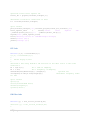
Table of Figures
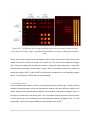
Figure II-1: 3-D Structure of the LEAC chip .......................................................................................... 12
Figure III-1: LEAC chip mask designs .................................................................................................... 14
Figure III-2: Comparison of the single versus segmented buried detectors ........................................ 15
Figure III-3: Zoomed in view of the most used metal mask design ..................................................... 16
Figure III-4: Cross-sectional view of an SOI wafer................................................................................ 17
Figure III-5: Via etching procedure for exposing pads for probing ...................................................... 18
Figure IV-1: Submitted mask design (left) and single, zoomed in view of channel design (right) ....... 20
Figure IV-2: Molecular structure of PDMS ........................................................................................... 21
Figure IV-3: Capillary flow through microfluidic channels4 ................................................................. 22
Figure IV-4; Active fluid flow apparatus configuration ........................................................................ 23
Figure IV-5: Still shot from video of moving fluorescent particles ...................................................... 24
Figure IV-6; Fluorescing capillary fluid flow through permanently bound PDMS on glass slide (left)
and fluorescing active fluid flow through permanently bound PDMS on LEAC chip (right)................ 25
Figure IV-7: PDMS-chip aligner ............................................................................................................ 26
5|Page
Figure IV-8: Chip mask design (left), PDMS mask design with cutting guide (center) and actual PDMS
aligned to chip and permanently bound from plasma oxidation (right) ............................................. 27
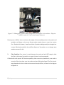
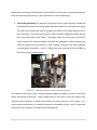
Figure V-1: Original probe station where each probe has independent, cantilevered XYZ motion.
With magnets holding the probes in place on the large steel base, one probe was used to apply a
potential to a “common” pad on the LEAC sample as the second was brought ................................. 28
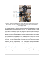
Figure V-2: Photograph of the sample holder and fiber launch system with translational and
rotational stages that provided the necessary movement of the sample for appropriate alignment 30
Figure V-3: Photograph of probe station configuration at this phase in its evolution. The piece
labeled “metal slat” has vertical motion allowance. ........................................................................... 31
Figure V-4: Block diagram of probe station configuration and portions with movement .................. 32
Figure V-5: Probes are aligned and in contact and the fiber is aligned to the waveguide, prepared for
proper coupling of the laser................................................................................................................. 33
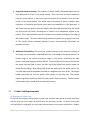
Figure V-6: Pump positioned above probe card with tubes running through the epoxy ring and into
the sample. The piece of tubing not connected to the syringe pump is held in place by a secured
magnetic clamp. ................................................................................................................................... 35
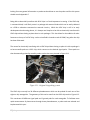
Figure V-7: Mechanical fixtures on microscope objective ................................................................... 36
Figure VI-1: Original chip probing system ............................................................................................ 38
Figure VI-2: Mask design of the LEAC chip with color coding where red indicates signal pads, green
indicates ground pads, and purple indicates the approximate locations of edge sensor touchdown 39
Figure VI-3: New probe card ordered to specifications ....................................................................... 40
Figure VI-4: Top view of the probe card showing probes and epoxy ring configuration (left) and a
microscopic view of the probes in contact with LEAC chip pads and an edge sensor shown on the
right hand side (right) .......................................................................................................................... 41
Figure VI-5: Bent probes ...................................................................................................................... 44
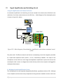
Figure VII-1: Block diagram of the multiplexing, amplification, and software automated control
system .................................................................................................................................................. 45
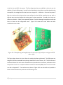
Figure VII-2: Multiplexing and Amplification Circuit before (left) and after redesign and PCB order
(right) ................................................................................................................................................... 46
Figure VII-3: Interface cable to connect the probe card to the switching circuit ................................ 47
Figure VII-4: Version 1.0 of LEAC Data Recording and Control VI ........................................................ 48
Figure VIII-1: Antigen-antibody reaction with secondary antibodies .................................................. 50
Figure VIII-2: Molecular structure of chip surface treatment .............................................................. 51
Figure VIII-3: ESAT-6 and AG-85 antigen-antibody assay with rat-α-mouse control line: full assay
fluorescent image (right), cropped and labeled fluorescent image of TB antigen-antibody assay .... 52
Figure VIII-4: Combined fluorescent images of assay using hand printing and microfluidic channels
showing ESAT-6 binding with itself (lower right) and α-AG-85 crosslink binding with ESAT-6 (upper
left) ....................................................................................................................................................... 53
Figure VIII-5: Fluorescent image of ESAT-6 and α-ESAT-6 binding in channel widening from assay
using PDMS printing with microfluidic channels ................................................................................. 54
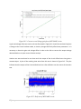
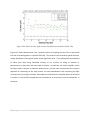
Figure IX-1: Current versus Voltage gain plot of MUX/AMP circuit ..................................................... 56
6|Page
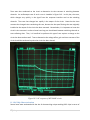
Figure IX-2: Drift test of MUX/AMP circuit .......................................................................................... 56
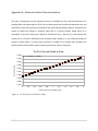
Figure IX-3: RC response of MUX/AMP circuit ..................................................................................... 57
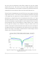
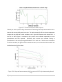
Figure IX-4: Typical IV curve of a LEAC chip before and after annealing. Y-axis is the magnitude of
the current ........................................................................................................................................... 58
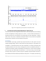
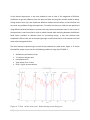
Figure IX-5: Time series of data from photodetector when the microscope was switched from on to
off in the middle of the test ................................................................................................................. 59
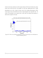
Figure IX-6: Dark currents, light currents and photocurrents from a LEAC chip ................................. 60
Figure IX-7: Photocurrents from a LEAC chip test................................................................................ 61
Figure IX-8: Sequential measurements of dark currents on LEAC chip demonstrating thermal drift . 61
Figure IX-9: Magnitude squared of filtered and unfiltered data ......................................................... 63
Figure X-1: Schematic of location of PCB that needs to be modified to invert circuit ........................ 68
Table of Figures (Appendix)
Figure A. 1- Diagram showing the interdisciplinary team dynamic of the LEAC project ..................... 74
Figure A. 2: Gantt chart of Spring Semester ........................................................................................ 75
Figure A. 3: PDMS Mask design drawn in LASI..................................................................................... 77
Figure A. 5: LEAC chip schematic ......................................................................................................... 78
Figure A. 6: Simplified 2D diagram of adjustments made to configuration 1 necessary to measure
WG 1,4,5,6 (left) and a photograph of the probe station in configuration 1 with the sample holder
shown on the bottom right, fiber launch on the bottom left, and probe ca....................................... 79
Figure A. 7: Block diagram of configuration 2 (right) and photograph of the probe station in
configuration 2 (left) ............................................................................................................................ 80
Figure A. 8: Block diagram of configuration 3...................................................................................... 81
Figure A. 9: Coordinate definition for alignment instructions with the lucky testing dinosaur, Lenny
.............................................................................................................................................................. 81
Figure A. 10: Probe card as received from Alpha Probe ...................................................................... 85
Figure A. 11: Image showing the probe card probes being cleaned and the resulting marks ............ 87
Figure A. 12: Circuit schematic for the multiplexing and amplification functions .............................. 90
Figure A. 13: Top traces of PCB ............................................................................................................ 91
Figure A. 14: Bottom traces of PCB ...................................................................................................... 91
Figure A. 15: BOM of MUX/AMP Circuit .............................................................................................. 92
Figure A. 16: Front Panel of LEAC Data Recording and Control v1.0 ................................................... 93
Figure A. 17: Sample section of coded wires from the LabVIEW program .......................................... 96
Figure A. 18: Flow Chart of LabVIEW code .......................................................................................... 98
Figure A. 19: Plasma Chamber ........................................................................................................... 103
Figure A. 20: Inside Plasma Chamber ................................................................................................ 105
Figure A. 21: Use of micropipettes .................................................................................................... 106
7|Page
Figure A. 22: Knocking off PDMS solution ......................................................................................... 107
Figure A. 23: Stirrer apparatus with various beakers ........................................................................ 107
Figure A. 24: Budget Table ................................................................................................................. 109
Figure A. 25: RI of Sucrose Diluted in Water...................................................................................... 110
Figure A. 26: Run 1 of the sucrose test. Stems showing events during test ..................................... 112
Figure A. 27: Run 2 of the sucrose test. Stems showing events during test ..................................... 113
8|Page
I.
Introduction and Motivation
With the extent of advancements made in both the pharmaceutical and diagnostic testing
industries, it is surprising that there are still 1.7 million tuberculosis-related deaths per year,
worldwide and only 60% detection of all TB-infected individuals.1 This disparity between infection
and its detection can be largely attributed to a combination of insufficient point-of-care diagnostics
and TB’s predominance in impoverished regions of the world where resources for testing and
treatment are limited. Current methods of diagnosing TB include the skin test, blood testing, chest
x-rays, and sputum cultures, all of which have their limitations.2
The skin test is the most common method for initially diagnosing a TB infection, but it cannot
effectively distinguish between different stages of the disease including recent exposure, latent
versus active infection, or drug-resistant TB forms. For this test, a small amount of purified protein
derivative (PPD) of the bacterium is injected intradermally, with a positive result indicated by a
swelling at the site of PPD injection after 48-72 hours.2 Unfortunately, there is a large incidence of
false positive results in patients who have had the BCG vaccine or who are infected with a latent
form of TB and false negative results in immunosuppressed patients or individuals so recently
infected that their immune system has not yet reacted to the bacteria. The other secondary forms
of TB testing are limited by either expense, the need for a skilled technician or doctor, time needed
to obtain results, or a combination of those thereof. Due to the pitfalls of the current testing
methods available, it is clear that there is a formidable need for an innovative diagnostic strategy
that could provide rapid, affordable, and robust testing with the ability to differentiate between
different stages of the disease.
The lab-on-a-chip diagnostic biosensor described in this paper employs a novel strategy for
detecting diseases using label-free technology in real-time and has high potential for application in
the medical industry. The underlying physical phenomenon for this device is the detection of a local
field shift using photodetectors and a waveguide with total internal reflection of coupled light.
When a nanolayer of biomolecules is added to the surface of the waveguide, a change in effective
refractive index causes a shift in the evanescent field distribution, which is then detected as a
change in photocurrent at the underlying detectors.3
9|Page
With increasing research finding differences between molecular signatures of active, latent, and
uninfected TB samples4,5,6, this device has even greater potential in potentially making it feasible to
not only identify TB-infected individuals, but to distinguish between those with the latent versus
active form. Previous work on the original LEAC chip design found that a change in a thickness on
the surface of waveguide as small as 30 pm, can be detected, which corresponds to a detection limit
of 120 pm.3 In refining and optimizing the measurement methods and electronics of the LEAC chip,
integrating microfluidics for real time detection, and developing LabVIEW for a more user-friendly
interface, the scope of application for this technology could be vast.
In addition, because
complementary metal oxide semiconductor (CMOS) technology is no longer cutting-edge, the cost
of mass-producing chips like the one used in this project would be quite low, around $2.507, making
this a feasible method for improving point-of care diagnosis in third world countries.
Thus, the goals of this project were vast, as no senior design work had been done previously on this
project.
The goals can be summarized into the following categories, but are by no means
exhaustive and all goals were selected with the aim of either making the device more attractive to
the medical industry or more automated and easier to use for future experimentation.
1. LEAC Chip Fabrication
To optimize fabrication techniques to obtain a successfully repeatable procedure in
producing chips with consistent behavior
2. Microfluidics Integration
To design a master mold for channels, confirm fluid flow, and integrate the channels with
the chip for the realization of real-time testing and rapid sample delivery
3. Development of Probe System
To build a mechanical structure for aligning all elements of the testing apparatus,
accommodating for changes to the probing system and the incorporation of microfluidics on
the surface of the chip
4. LabVIEW Automation of Data Collection
Develop LabVIEW code for multi-channel testing and a more user-friendly data acquisition
and review. This involves the software interfacing with the hardware and automatically
switching between the individual channels on the probe card and LEAC chip
10 | P a g e
4. Improvements to Original Circuitry
To layout and make a printed circuit board, amplify the signal to a readable level, and design
and order a probe card to interface with the circuit to improve the overall quality and
efficiency of data collection
5. Biomolecular Patterning Strategies
To develop successful methods for patterning onto the waveguide’s surface and to test for
the specificity and sensitivity of two different TB antigen-antibody complexes
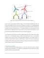
Achieving these goals required a collaborative and interdisciplinary team dynamic encompassing
expertise from electrical, chemical, biological, and mechanical engineering. To establish good
communication between different aspects of the project, multiple, weekly team meetings were set
and progress reports submitted. Team leadership was altered throughout the year and a detailed
Gantt chart was made together to keep the project on a schedule while also recognizing critical
paths that could play a role in setting back other parts of the project. The realization of the above
goals, including the setbacks and problems encountered with each, are detailed in the following
sections of this report. More detail on project management can be found in Appendix A.
II.
Background
A. Local Evanescent Array Coupled (LEAC) Chip Theory
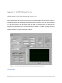
The local evanescent array coupled (LEAC) chip operates by sensing changes in the optical
properties of materials in contact with it.
This means that the target substance need not be
labeled in order to detect the presence of it. This feature has the advantage of not only preserving
the biomolecule for any further testing, but it also reduces the cost as labeling technologies can be
quite costly.
11 | P a g e
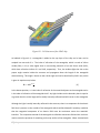
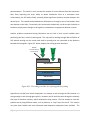
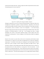
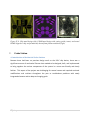
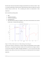
Figure II-1: 3-D Structure of the LEAC chip
As labeled in Figure II-1, a waveguide is added to the top layer of the chip and a laser can be
coupled into one end of it. The index of refraction of the waveguide, which is made of silicon
nitride (SiNx), is 1.8, a value higher than its surrounding materials of air and silicon oxide (SiO2),
which have refractive indices of 1 and 1.48, respectively. Thus, the incident light that hits at the
proper angle remains inside the structure and propagates down the length of the waveguide
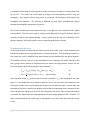
without exiting. This angle is known as the critical angle and can be described by Snell’s Law, which
is given in equation one, below.
[1]
In the above equation, nt is the index of refraction of the material adjacent to the waveguide and ni
is the index of refraction of the waveguide itself. Any light incident on the boundary that is equal to
or greater than the critical angle will be totally internally reflected and will remain in the waveguide.
Although the light is totally internally reflected in the structure, there is a component of the electric
field that is present on the outside of the waveguide which satisfies Maxwell’s boundary condition
that the tangential component of an electric field must be continuous across the materials’
interface. The component outside of the waveguide is called the evanescent field and this is what is
used to sense the presence of something on the top surface of the waveguide. When a biomolecule
12 | P a g e
is attached to the surface of the waveguide its index of refraction increases to a value greater than
air’s RI of 1. This causes the critical angle to change in the corresponding location along the
waveguide. Since physics requires that power be conserved, the evanescent field beneath the
waveguide must decrease.
This decrease is detected by small silicon photodetectors placed
beneath the waveguide, as depicted in Figure II-1.
The silicon’s resistance will increase because there is less light from the evanescent field coupled
into the device. This will in turn result in a lower current detected for a specific detector, which is
manually biased at some optimal voltage. Using a probe card, the user can individually switch
between detectors and locally measure the corresponding photocurrent changes.
B. Modulation of the Laser
An improved method of measuring the photocurrent from the LEAC chip involves modulating the
laser diode coupled into the waveguide with a function generator. This modulating frequency is
then input into a lock-in amplifier along with the total current obtained from the buried detector.
The amplifier will then “lock in” to the modulated current’s frequency and phase induced by the
laser, giving a direct readout of the photocurrent no matter how large the dark current may be.
This phenomena is described by equations two and three.8
[2]
(after LP Filter)
[3]
In the equation above, Vpsd is the output of the lock-in amplifier, Vsig is the amplitude of the input
signal, VL is the amplitude of the reference signal, θsig and ωr are the phase and frequency of the
input signal, and θref and ωL are the phase and frequency of the reference signal. It can be seen that
the output of the lock-in amplifier will produce a DC voltage corresponding to the component of the
input and reference signals that are of the same frequency and phase. Due to time and resource
constraints, this method was not implemented by the senior design group this year. However, it is
highly recommended that this technique be employed for any future work done with the current
circuit.
13 | P a g e
III.
LEAC Chip Fabrication
The LEAC chips used in all experiments were manufactured in Colorado State University’s Electrical
and Computer Engineering cleanroom by both graduate and undergraduate students. Standard
cleanroom procedures and processing were used. Some of the more critical steps are described
below and the full fabrication flow can be found in Appendix B.
A. LEAC Chip Layout
The layout of the current LEAC chip design was designed by Rongjin Yan. The design was chosen to
allow for significant processing error in the cleanroom as well as to provide for a variety of
waveguide and buried detector sizes and structures. Having multiple waveguides and detectors
types allowed for experimentation with numerous variables without having to order and process
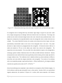
different mask designs each time. The mask used to fabricate the chips was a 3 by 3 grid consisting
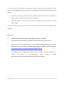
of 9 unique designs, as pictured in Figure III-1.
Figure III-1: LEAC chip mask designs
The bottom left sector of the mask contains the nine designs needed to create the buried detectors.
A zoomed in image of the buried detectors is shown below in Figure III-2.
14 | P a g e
Figure III-2: Comparison of the single versus segmented buried detectors
The two solid structures on the left produce a single buried detector structure beneath the
waveguide of silicon once the fabrication is completed. It is these single detectors that were used
in the experiments conducted on the LEAC chips. These detectors were selected because their
layout prevents the waveguide from having a vertical step to cross for every detector. This vertical
step has been shown to increase scattering from the waveguide, which results in less power
reaching the farther regions. This scattering and reduction of power is undesirable as the largest
amount of laser power possible needs to be coupled along the waveguide to ensure a quantitatively
measureable evanescent field.
The top left quadrant of Figure III-1 contains the mask designs for the metal layer. The one used
primarily for this project was the mask nearest the middle, of which a magnified view can be seen in
Figure III-3, below.
15 | P a g e
Figure III-3: Zoomed in view of the most used metal mask design
This particular mask was also used several reasons. First, the design’s location near the middle of
the mask makes it much easier to use with the small-range mask aligner machines that were
available in the CSU cleanroom. Second, the pad sizes of this mask were optimal for the current
LEAC chip testing equipment. The pads of this mask, though still only 100um wide, were a much
heftier 290um tall when compared with the 100um of the other designs. This allowed for a much
higher degree of rotational alignment error when bringing the probes into contact with the
fabricated chip’s metal pads. Finally, this version of chip pads was chosen for its lack of structures
in the middle of the chip. This feature was very useful when dealing with the old and likely
inaccurate PECVD machine in the cleanroom. This large open space allowed for a region large
enough to use the Filmetrics device to measure layer thicknesses on the chip. This measurement
not only confirmed that enough material had been deposited onto the chip, but also allowed for
observation of the etching progress after small steps. This advantage will become obsolete once
consistent fabrication flows are completely developed and characterized, but is invaluable for the
current stage of fabrication.
The bottom right quadrant of the mask design pictured in Figure III-1 creates the waveguide. All
nine of these masks are very similar to each other, differing only in the width of the waveguides.
Different widths were used in fabrication throughout the year, but once experimentation was
16 | P a g e
feasible, the 5um waveguide width was needed to increase the chances of successful laser coupling
after polishing the chip as best was possible. The masks can create waveguides that range from 2.5
to 5.5 um wide.
Finally, the last quadrant of the mask design, the upper right quadrant of Figure III-1, represents the
via layer. This layer is the very last step in chip fabrication as it is the mask used to etch material
down to the metal pads to expose them for probing. The differences between these masks are the
height of the vias so that one matches to each corresponding metal pad height, whose differences
were discussed previously. Another difference of note was whether the middle area of the mask
would be exposed during etching. This variable will be further investigated in future experiments
for optimizing fabrication flow and end products.
B. Problems Encountered During Fabrication
A number of problems were encountered during fabrication in the past year. An attempt will be
made in this section to briefly go over as many of these problems as possible and perhaps offer
potential paths to try for future fabrication efforts.
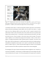
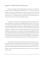
The first problem encountered during the fabrication of the LEAC chip this year was the lack of
availability of the desired wafer type. A silicon-on-insulator (SOI) chip within the means of the
project budget was sought for several months before finding a suitable solution. An example of an
SOI chip is pictured in Figure III-4.
Si (SOI, Device Layer)
SiO2 (Insulator)
Si (Wafer Substrate)
Figure III-4: Cross-sectional view of an SOI wafer
SOI was desired because it would most likely be single crystal silicon. This would be advantageous
for the LEAC chip for its lack of grain boundaries in the silicon layer, which makes for a much better
17 | P a g e
photoconductor. This would, in turn, increase the amount of current induced from the evanescent
field, likely improving the chip’s ability to detect bimolecular films at a nanometer level.
Unfortunately, the SOI wafers finally received yielded significant thickness variation between the
device layers. This caused the buried detector thicknesses to change by tens of nanometers from
one detector to the other. Fortunately, this issue should, theoretically, not be a major limitation as
the device simply senses changes in the signal on each detector as opposed to absolute currents.
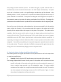
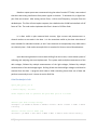
Another problem encountered during fabrication was the lack of etch control available when
performing the final, critical via etching step. This step calls for etching through 200 to 1500 nm of
SiO2 without etching into the metal pads used for probing that are connected to the detectors
beneath the waveguide. Figure III-5, below, displays the etching process described.
AZ2070
Prevents Etching
of rest of chip
HF
HF
AZ2070 Photo Resist
SiO2 (Insulator)
Aluminum (Metal Pad & Wires)
SiO2 (Insulator)
Si (SOI, Device Layer)
SiO2 (Insulator)
Si (Wafer Substrate)
Figure III-5: Via etching procedure for exposing pads for probing
Hydrofluoric acid (HF) was initially employed in an attempt to etch through the SiO2 because it is
strong enough to etch through glass quickly. However, the HF could also etch through the relatively
thin layer of aluminum contacts, which rendered the chips useless. The first attempt to solve this
problem was by using different metals, such as platinum, as “stop” layers for the HF. This solution
may have been feasible had more advanced metal deposition equipment been available. The
18 | P a g e
electron beam evaporation system in the CSU cleanroom was not working and many of the
neighboring university labs only had aluminum available for deposition. This problem was finally
overcome by purchasing a commercial etchant called SILOX VAPOX III from Transene.9 This proved
to selectively etch the SiO2 over the aluminum.
IV.
Microfluidics Fabrication
One of the primary goals for this lab-on-a-chip device was to bring the unit into real-time detection.
In previous experiments, the LEAC chip’s technology was confirmed by laying a solution of antibody
down over the entire chip and, after appropriate incubation, printing a corresponding antigen to
the surface with a microarray printer.10 This technique, though useful as a proof of concept test that
had a detection limit of 120 pm, is not feasible for actual implementation of the device in the
medical field. By designing and integrating a microfluidics element to the device, a blood or serum
sample could potentially flow through channels of micrometer width for delivery to the waveguide
wherein any present antibodies in solution corresponding to the antigens printed to the waveguide
would bind and be detected by a change in photocurrent.
A. Microfluidics Mask Design
The first step towards achieving real-time detection on the LEAC chip was to design and order a
mask for microfluidic features. The original mask design had to be small enough to fit within
approximately 9.5 cm11 so as to not cover the metal pads, which would prevent probing and, thus,
measurement. Because the features used up all available space, a cutting guide was also added to
improve the precision of the by-hand cutting with a razor blade. The channels were designed to run
parallel to each other, but to cross the waveguide perpendicularly. This feature of the mask enables
the device to potentially detect multiple antigen-antibody complexes on the same waveguide
nearly simultaneously. Figure IV-1 shows the final mask designs. Of the 32 individual pieces, there
are eight each of four different designs. The four designs vary only in spacing and number of
channels. Different designs were selected for fluorescent assay imaging versus chip use and having
multiples of each design made for more efficient production.
19 | P a g e
Figure IV-1: Submitted mask design (left) and single, zoomed in view of channel design (right)
For integration with a working LEAC chip, the bottom right design in Figure IV-1 was used. With
only a single syringe pump, the designs with extra channels were not necessary. This design was
picked over the other 4-channel design because the outer channels were positioned closer to the
edge and, consequently, the expanded width crosses the waveguide closer to where the laser was
coupled. This proved beneficial because the power and photocurrents have larger and more
quantitatively measureable values at the start of the waveguide than at the end. The power
decreases as light continues to propagate down the waveguide. All channels measure 100 m in
width and expand to 570 m at the widest part where they traverse the waveguides. The
expansions serve two purposes. First, they allow for a wider detection region on the waveguide by
overlying a greater number of detectors than if the 100 m width had been maintained. Second,
the expansion causes the fluid flow to slow significantly and this slowing of the sample provides for
a longer residence time. This residence time is needed to allow any present antibody to diffuse to
the surface and react with the antigens attached to the waveguide. The reaction of an antibody
and its corresponding antigen is governed by kinetics. Affinity coefficients (kA) of antigen-antibody
reactions are typically on the order of 103 – 105 M-1sec-1.11
Once the mask design was completed, it was ordered as a transparency from Fineline Imaging. An
SU-8 mold was made by spin-coating SU-8 onto a silicon wafer. Because SU-8 is an epoxy-based
negative photoresist, the portions in Figure IV-1 in white, which were exposed to UV became
20 | P a g e
insoluble in the developer leaving a mold of raised channel features approximately 35 m tall. The
full procedure for making an SU-8 master mold can be found in Appendix C along with more
detailed dimensions of the channel mask design.
An SU-8 mold was originally made in the CSU cleanroom. However, due to limitations on the
maximum wafer size that could be spun, the mold used for all future work was made using softlithography in another lab on campus because using full, circular wafers provided a more even
coating than silicon wafers cut down in size. Because 32 pieces are made at once, having a more
even surface yielded more uniform features among batches. The SU-8 mold created from softlithography was then used to create a reusable master mold out of polydimethylsiloxane (PDMS).
PDMS is a nontoxic, optically transparent polymer that was used in all microfluidics fabrication for
the device.
PDMS has a refractive index around 1.4, a feature of note for any baseline
measurements of the chips. The chemical formula of PDMS is shown in Figure IV-2, below, where
the bracketed ‘n’ term represents the repeated monomer unit with typical values between 90 and
410.12
Figure IV-2: Molecular structure of PDMS
B. Fluid Flow
The channels designed for the lab-on-a-chip device were compatible for either passive or active
flow and both types were used for experiments. The advantages to capillary flow are its simplicity,
independence from bulky pumping setups, and small sample requirements. Capillary flow is
introduced to the microfluidic system by adding a small volume of fluid, often less than 3 L, to the
larger inlet reservoir with a pipette.
The channel fills spontaneously by capillary force and
differential capillary pressure and fluid evaporation serve to sustain fluid flows with relatively
21 | P a g e
constant rates for about 30 minutes. Figure IV-3 depicts the effect of passive flow and the creation
of evaporating menisci in the two reservoirs.13
Figure IV-3: Capillary flow through microfluidic channels4
Although the evaporation can serve as an important driving mechanism for fluid flow, there can be
consequences of evaporation on protein or analyte concentration. Evaporation on the inlet side
can be limited by adding a small film of mineral oil over the sample fluid. Passive flow was used for
all immunoassays, which are detailed in section VII and Appendix I.
It was found through
fluorescent imaging that fluid would not flow passively through the PDMS channels when either
reversibly or irreversibly bonded to a LEAC chip.
It was suspected that either a strongly
hydrophobic chip surface or chip features significant enough to hinder capillary forces were
responsible for preventing flow. Further investigation of this phenomenon should be investigated
in the future
Because of the restraints on passive flow and the need to continuously switch between sample
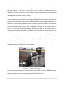
concentrations for a specific test, active flow was implemented for this device by employing a
syringe pump. The available in-house pump was reconfigured to pull fluid through the channels
rather than to push it through to ensure a better seal between the PDMS and chip. Figure
IV-4shows a schematic of the pumping system where PEAK tubing extends from one reservoir to
the sample and from the other reservoir to a syringe with a luer lock connection.
A small
modification was made during fabrication – 0.8 mm punches were used on either end to provide a
tight seal around the tubing as opposed to the 1.5 mm inlet and 1.0 mm outlet punch sizes typically
used for capillary flow. The pump works by pulling up on the syringe plunger thereby creating a
22 | P a g e
vacuum, which causes fluid to flow from the sample container, through the channels, and up into
the syringe. Throughout the development of the system configuration, larger syringes were found
to allow for more sustained periods of testing.
Figure IV-4; Active fluid flow apparatus configuration
For both types of flow, the movement of fluid can be modeled by equation four, which relates
volumetric flow, Q, to a pressure difference and a resistance term, K.
Qf
P
K
[4]
The resistance term, K, represents the viscous and frictional resistances within the channel to
laminar
flow, neglecting the expansions at the waveguide interface. This term is given by equation
five.13
1
nh
12L 192w
K 3 1 5
tanh2w
w h h n 1,3,5...
[5]
In equation five, represents the dynamic viscosity of the fluid and the w and h terms have been
derived
to replace a radius term because the channels are rectangular ducts instead of circular
pipes. The setup used for LEAC chip testing had a K-value approximated at 4.561014 kg/m4s. For
active flow with a syringe pump, the volumetric flow could be altered by adjusting the speed of the
23 | P a g e
upward displacement of the syringe plunger. The pump used for active flow had a range of 5 - 200
m/s. Equation six was derived using the ideal gas law and syringe geometry to relate the change
in syringe pressure to the pump’s speed setting x, which can then be used with equation five to
relate the pump’s speed setting to volumetric flow of the fluid.
Psyringe
nRT
D2
x
4
[6]
Analysis of the syringe pump velocity and volumetric flow rate using the above equations generates
an approximation that follows a linear relationship. The fluid flow rate can overcome viscous and
frictional resistances at the same rate as the pressure difference is pulling at the lowest possible
syringe plunger speed, which was 5 m/second. Even at this lowest setting, some backpressure
builds up, as was confirmed experimentally. When the syringe pump was stopped, fluid continued
to flow because there was still an unequilibrated systemic pressure difference.
C. Fluid Flow and Leaking
Using both large fluorescing particles and a solution of polyclonal IgG antibody fluorescently labeled
with Alexa fluor 488, fluid flow was confirmed and channel leaking was investigated. The fluid flow
imaging was one of the first tests conducted to confirm that the channels created by the new mask
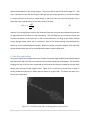
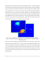
design were functional under capillary flow. Figure IV-5 is a still shot removed from a video of
moving fluorescent particles in PDMS channels bound to a glass slide. The video was taken on a
fluorescent microscope.
Figure IV-5: Still shot from video of moving fluorescent particles
24 | P a g e
As the integration of the device progressed, permanent binding became an increasingly critical
component of the design. Without permanent binding, more significant leaking occurred out of the
channels, which would could short circuit the probe pads or make measurements indistinguishable
from one another on the actual chip. In addition, once it was established that active methods were
needed to achieve flow on the chip, a permanent bond was necessary to give the setup enough
rigidity. Before a better setup was introduced to relieve strain on the PEAK tubing, a bend or an
adjustment of the tubing was enough torque to pull the PDMS off of the chip.
A successful, irreversible bond between the chip and PDMS was first achieved on non-working chips
by plasma treating both the chip and PDMS with 18 seconds of plasma oxidation at 20 watts with
the plasma machine located in Scott Lynn’s laboratory. During plasma oxidation, oxygen radicals
attack the surfaces, rendering them more hydrophilic. The plasma oxidation adds silanol groups
(SiOH) to the PDMS and when attached to the chip, the bonds eventually relax to their normal
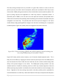
state, resulting in a permanent bond. Figure IV-6 shows a fully fluorescing solution of labeled
antibodies running through the channels with a permanent bond on both a glass slide and a chip
with no evidence of leaking.
Figure IV-6; Fluorescing capillary fluid flow through permanently bound PDMS on glass slide
(left) and fluorescing active fluid flow through permanently bound PDMS on LEAC chip (right)
Difficulties were encountered once working chips were finished with the commercial etchant. The
plasma oxidation techniques that worked on older chips, glass slides, and unaltered SiN x pieces did
not work to permanently bind the new chips to PDMS. Several measures were taken to eliminate
all surface treatment variables and it was concluded that the surface chemistry of the chip must
have been altered by the new fabrication process to make the originally successful plasma oxidation
25 | P a g e
technique invalid. It is also possible that an organic scum was present on the surface, although
extensive cleaning of the chips with sonication and high-powered plasma oxidation were
attempted. This issue is still in the process of being resolved and will need to be reinvestigated
once additional chips are fabricated for testing.
Another problem encountered with the permanent bonding technique was that the working plasma
treatment was conducted in a different lab where there were no mask aligners like those in the
cleanroom. This presented an obstacle because a relatively high level of precision was needed to
successfully integrate PDMS channels with a chip without covering the metal pads needed for
probing. To ensure the best possible binding, it was desired to align and the PDMS inside of the
metal pads and introduce binding within 1.5 minutes of the removal of the chip and PDMS from the
plasma chamber. Alignment by hand and with the naked eye was attempted on non-working chips
and although close alignment was achieved, some pads remained covered by PDMS. To mitigate
this problem, a simple alignment system was designed by combing xyz-translational stages for fine
tune positioning of the chip, a glass slide holder to which the PDMS would be reversibly attached
and upside down, and a magnifying lens to better visualize the alignment. An image of this
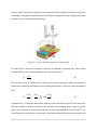
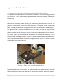
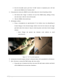
mechanical apparatus is depicted in Figure IV-7, below.
Figure IV-7: PDMS-chip aligner
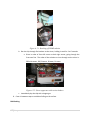
Figure 4.8 shows the mask designs of the chip and channels as well as a piece of PDMS permanently
bound to a working chip using the alignment device pictured in Figure IV-7.
26 | P a g e
Figure IV-8: Chip mask design (left), PDMS mask design with cutting guide (center) and actual
PDMS aligned to chip and permanently bound from plasma oxidation (right)
V.
Probe Station
A. Introduction to Mechanical Probe Stations
Because there had been no previous design work on the LEAC chip device, there was a
significant amount of mechanical fixtures that needed to be designed, built, and implemented
to bring together the various components of the system in a more user-friendly and timely
fashion. This aspect of the project was challenging for several reason and required continual
modifications and revisions throughout the year to troubleshoot problems with newly
integrated elements and to adapt to changing goals.
27 | P a g e
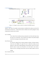
Figure V-1: Original probe station where each probe has independent, cantilevered XYZ motion.
With magnets holding the probes in place on the large steel base, one probe was used to apply a
potential to a “common” pad on the LEAC sample as the second was brought
A mechanical probe station is a device that physically acquires signals from a semiconductor
devices with precise positioning of probe needles onto the surface of the device. 14 A probe
station can sit on a laboratory table or can be a table in of itself. In general, some part of the
probe station is fixed in place and another plane of the station will move very precisely with
respect to the stationary portion. A microscope is usually mounted on the station or the table
and allows the user to view the probes as they make contact with the sample. This precise
motion capability can be achieved with springs and micrometers, similar to those used in
calipers, or through the piezoelectric effect if greater precision is required. Prior work on the
LEAC project had been performed on a table-mounted probe station that implemented two
independently manipulated manual probes and a manual or piezoelectrically-controlled fiber
launch, as shown in Figure V-1, above. One probe was brought into contact at a time followed
by precise movement of the fiber into position to couple the laser into the waveguide.
The advantages of this type of sample-centered probe station configuration are it’s simplicity in
construction and flexibility. Unfortunately, the ambitious goals of this senior design team could
not be achieved with such a system. One of the primary goals of this project was to streamline
28 | P a g e
the probing and data collection process. To achieve this goal, a probe card was used to
simultaneously connect to several active areas on the LEAC sample simultaneously. The probe
card’s role in the device as well as its specific design considerations will be discussed in the
following section. In brief, a probe card is a printed circuit board (PCB) that has an array of
probes attached to its underside. These probes are designed and configured to correspond to
the connection areas on the device for testing, metal pads of the LEAC chip. The design of a
probe station that could utilize such a probe card is more involved than the one originally used.
Some of the most critical probe card considerations that were accounted for by the probing
station include the linearity of the connection pads with respect to the probe card and the
planarity of the sample surface with respect to the plane of the probes. The probe station
needed to allow for precise vertical motion to bring the aligned probe card and sample into
contact with each other. The other primary goal of this senior design team was to integrate
microfluidics onto the LEAC chip to give the device real-time data collection capabilities in
responding to a change in refractive index when fluid or a layer is present on the surface of the
waveguide. Successfully accomplishing this systematic integration required intensive revision
of the probe station. The probe card and microfluidics encompassed the goals that were the
driving force for to the evolutionary design process of the probe station.
B. First Probe Station Configuration Without Microfluidics
The following entails the original specifications for the probe station as well as the steps taken
to meet those specifications.
1.
Linearity: Linearly align the LEAC sample contacts to the probes of the probe card.
The strategy implemented to ensure linearity was to fix the probe card in a position that was
parallel to the edge of the probe station and then move the sample with respect to it
using a rotation stage mounted to an XY manipulation stage. XY motion enabled
movement of the sample into a roughly accurate position under the card. The rotation
was then employed to linearly align contacts to all of the 32 probes. Figure V-2 shows
these physical configurations of the probe station.
29 | P a g e
Figure V-2: Photograph of the sample holder and fiber launch system with translational and
rotational stages that provided the necessary movement of the sample for appropriate alignment
2.
Planarity and Contact: Allow precise vertical motion to bring probes and sample into
contact while ensuring acceptable planarity tolerances.
The required vertical motion was provided through the use of the metal platens of the original
probe station which could move vertically with respect to the table surface. Once the
sample is properly aligned, the probe card is brought down into contact with it. A
benefit to this design is that it allows the microscope to stay in focus on the sample
during the entire setup procedure, something that becomes critical in subsequent steps.
The use of the platens provided a unique balance between travel distance and precision;
they can travel at least 4’’ with a precision under 10 microns, while other similar
translation stages could only provide about 1.5’’ of travel at the same level of precision.
Figure V-3 shows the probe card and metal slat that provides it with vertical motion for
pad contact.
30 | P a g e
Figure V-3: Photograph of probe station configuration at this phase in its evolution. The piece
labeled “metal slat” has vertical motion allowance.
Planarity was a difficult issue to solve as the weight of the extended portion of the probe card
tended to pull down on the more distant probes causing them to come into contact
first. Despite this feature, it was found that all probes could generally be brought into
contact effectively and within the safe flex distance of the probes, so no changes were
made to account for this.
3.
Fiber Coupling: Once contact is made between the probe card and LEAC sample, allow
the fiber to be moved into position to couple the laser into the waveguide.
A fiber launch with precise XYZ motion capability, either manual or piezoelectric, was used to
move the fiber into place once the probe card was effectively aligned. The fiber launch
was adapted such that its tallest structure was the optical fiber, as shown in the diagram
of Figure V-4.
31 | P a g e
Figure V-4: Block diagram of probe station configuration and portions with movement
The purpose of this design was to ensure that the fiber launch would not interfere with the
probe card alignment and that they would not contact or damage each other. A
microscopic image of the pads in contact with probes with successful alignment of the
fiber with the waveguide is seen in Figure V-5, below.
32 | P a g e
Figure V-5: Probes are aligned and in contact and the fiber is aligned to the waveguide,
prepared for proper coupling of the laser.
C. Problems Encountered With the First Probe Station Configuration
The first configuration of the probe station met the initial design specifications and was used
from late November 2010 until mid-March 2011 when integration of microfluidics began to be
realized. One of the problems encountered with this setup was that the initial alignment
procedure assumed it would be necessary to have the chip at the very center of the sample
holder rotational stage. To achieve this centered positioning, several layers of glass were
stacked and taped together. This led to some observed instability in the sample when trying to
make firm contact with the probes. The second problem was the proximity of the bottom of
the platen to the other pieces of hardware. As can be seen in Figure V-3, above, the probe card
was set so far to the right on the platen that the left side of the platen was almost touching the
sample holder when the probe card was in position.
D. Second Probe Station Design with Microfluidics Integration
To obtain real-time data from a LEAC sample, microfluidic channels, as detailed in section four,
needed to be integrated into the system described above without disturbing or conflicting with
any of the existing components. The marriage of semiconductor and circuit technologies with
33 | P a g e
microfluidics presented some unique challenges that dictated the design of both the probe
station and the details of the channel design.
It was found through preliminary calculations that active flow would be desirable as opposed to
capillary-driven flow. Active flow put greater strain on the bond between the PDMS and the
surface of the LEAC chip and to complicate matters further, the interfacing of tubing to the
PDMS channels tended to move the PDMS and sample, both of which were detrimental to
experimental results and the longevity of the equipment. The following provides a breakdown
of the major design concerns and troubleshooting solutions that were used to resolve the
issues.
1. Pump design: Must implement a pump system allowing active flow through the microfluidic channels.
As discussed in detail in section four, permanent plasma bonding between the sample
and the PDMS was explored with varying degrees of success. In addition, an improvised
syringe pump was implemented to create a vacuum capable of pulling fluid through a
channel. This was desirable as the vacuum tended to improve the bond between PDMS
and the chip whereas a pushing motion would have tended to disrupt the bond.
2. Pump Positioning: The tubing must be interfaced to the chip in a way that minimizes
the risk of breaking the seal or translating the sample.
In this stage of the design, the microscope would be moved at an intermediate step in
the alignment procedure to allow the pump system to move into position directly above
the probe card. PEEK tubing would then be carefully inserted through the hole in the
probe card while avoiding touching the probes and then held in place to avoid moving
the PDMS or the sample. This apparatus is shown in Figure V-6, below.
34 | P a g e
Figure V-6: Pump positioned above probe card with tubes running through the epoxy ring and
into the sample. The piece of tubing not connected to the syringe pump is held in place by a
secured magnetic clamp.
E. Problems Encountered With the Second Probe Station Configuration
This design was successful in the sense that it resolved the issue of providing active fluid flow
while preventing the tubes from moving the sample and, thus, damaging the probes or metal
pads. However, a problem not realized until an experiment was conducted was the alignment
of the fiber to the waveguide. Alignment of the fiber must be extremely accurate to allow
adequate coupling into the waveguide and it is this factor that dictates that the fiber should be
the last thing aligned as all other steps can move the sample enough to disrupt laser coupling.
Also, due to the sensitivity of the adjustment, it is impossible to manage without the use of a
microscope. This called for another drastic revision of the probe station and alignment protocol
because to allow the microscope to be in place throughout the experimental procedure
required a different design of the pump’s location, setup, and tubing strain relief.
F. Final Probe Station Configuration
The final state of the probe station was a product of the developing design specifications as
well as the increasing experience of team members assembling the apparatus. The final design
35 | P a g e
addressed the problems detailed above and provided for the necessary microscope placement
while also improving the function of the probe station in several other ways.
1. Microscope positioning: To allow the microscope to stay in place above the sample and
simultaneously stabilize the tubing, guides were fabricated from small aluminum piping.
They were cut to length and bent to configure and attach to the single objective lens of
the microscope. The aluminum piping then tapers inwards, guiding the tubing into the
inlet and outlet holes of the PDMS. This design allows the microscope to remain in
position above the interface between the fiber and waveguide, thereby enabling the
necessary monitoring of the quality of laser coupling throughout the setup sequence
and during data acquisition. Figure V-7 depicts the new mechanical fixtures added to
the objective lens as tubing guides.
Figure V-7: Mechanical fixtures on microscope objective
One setback of this setup is that it required greater lengths of tubing to account for the more
distant positioning of the pump. Longer tubing results in more time to clear the system of air
once the pump movement is initiated and reduces the sample capacity of the syringe. For a
single sample measurement, this would not present a formidable concern, but for continuous
switching of many samples, this might need to be addressed.
36 | P a g e
1. Improved sample mounting: The problem of sample stability discussed above was not
fully addressed until late in the design process. Once the team had more experience
using the probe station, it was found that the sample did not need to be in the very
center of the sample holder. This would only be necessary if drastic rotations were
necessary or translation was limited, which were not impedances in this apparatus. It
was found that the sample could be roughly and reasonably adjusted with the naked
eye and would only need a few degrees of rotation to be adequately aligned to the
probes. This made it possible to put the sample on more stable footing near the edge of
the rotation stage. The more stable footing allowed the probe card to apply more force
to the sample, which produced improved contact and essentially eliminated any
planarity concerns.
2. Additional Functionality: There was one problem common to all the early iterations of
the design not discussed nor addressed until late in the design of the probe station. The
limited range of the various translation stages in the system, specifically the fiber
launch, made actual alignment fairly difficult. Since the fiber motion was so limited and
the probe card was fixed in place, the fiber had to be moved into position under the
probe card by sliding a large metal plate across the table top of the probe station. This
non-ideal plate and the hardware attached to it weighed more than 30 lbs. The sample
holder would then be slid into position with respect to the other two. This process
requires significant familiarity with the system and is time-consuming. Future versions
of the probe station should work to resolve this feature.
VI.
Probe Card Requirements
A. Benefits of a Probe Card
To improve the original probing system, a probe card specified and ordered to enable interfacing
with the LEAC chip more rapid and efficient than was previously possible. Purchase of the probe
card required an investigation of critical probe card parameters and system requirements. Readers
37 | P a g e
looking for more general information on probe cards and how to use the probe card for this system
should consult Appendix E.
Being able to electrically interface with LEAC chips is of vital importance in testing. If the LEAC chip
is commercialized, it will likely come in a package with external leads which can be easily soldered
to a PCB or otherwise connected to external circuitry. While the LEAC chip is still in its early
developmental and testing phases, it is cheaper and simpler to be able to electrically interface with
LEAC chips without having to place them in such packages. This also allows for the addition of other
features to the top of a LEAC chip, such as microfluidic channels made of PDMS, long after the chip
has been fabricated.
The means for electrically interfacing with a LEAC chip without having to place it inside a package is
to have metallic pads on a LEAC chip, which connect to the desired signal paths. These pads can
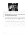
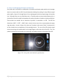
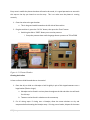
then be externally probed by metallic probes such as the ones pictured in Figure VI-1.
Figure VI-1: Original chip probing system
The LEAC chip currently has 39 different photodetectors which can be probed for each one of the
eight on-chip waveguides. The geometry of this can be seen from the LEAC chip mask in Figure VI-2.
This constitutes 39 different signal pads and 2 ground pads for each waveguide. To facilitate more
rapid measurement of photocurrent through these photodetectors, a probe card was ordered and
implemented this year.
38 | P a g e
Figure VI-2: Mask design of the LEAC chip with color coding where red indicates signal pads,
green indicates ground pads, and purple indicates the approximate locations of edge sensor
touchdown
Prior to integration of the probe card, making measurements with the LEAC chip entailed probing
individual pads with individual probes (Figure VI-1 shows a setup for accomplishing this) and
measuring the current across a photodetector for a specified voltage with each iteration. After the
implementation of the probe card, probing the first or last 34 photodetectors connected to any one
waveguide on the LEAC chip became a much rapid process that involved no adjustments one the
system was in place. All that is now required for measurements is to align the probes of the card
and make contact with the metal pads once and then use a system of multiplexers, amplifiers and
LabVIEW software to systematically measure the currents running through each individual
photodetector at a given applied voltage. More detail on the circuitry, LabVIEW interface, and
signal amplification can be found in the following section. Although the new probe card did require
a more complex probe station to precisely align a LEAC chip sample with the probes, once this was
implemented, acquiring large sets of data was facilitated and much more efficient.
39 | P a g e
B. Probe Card Design Specifications and Selection
Our probe card is essentially a configuration of precisely positioned probes which can be brought
down into contact with the LEAC chip simultaneously allowing for probing of many different signal
paths rapidly. Figure VI-2 through Figure VI-4 are photographs and microscope images of the probe
card. Although there are only 40 probes total, a 72-probe probe card was ordered because this is
the smallest size which would accommodate the required number of probes in the desired fashion.
These probes are epoxied into an aluminum ring which is connected to a PCB. The PCB has
dimensions 4.500” × 9.375” × 0.062” with a circular hole on one side to accommodate the epoxy
ring and probes. As seen in Figure VI-4, there are 32 probes in the central “block” of probes and 4
on the outside that are components of the two edge sensors. The rest of the PCB contains signal
traces connecting to the probes which end in edge fingers on the other side of the PCB. Thus, the
probes are electrically connected to by connecting a card edge connector to that side of the PCB.
Figure VI-3: New probe card ordered to specifications
40 | P a g e
Figure VI-4: Top view of the probe card showing probes and epoxy ring configuration (left) and
a microscopic view of the probes in contact with LEAC chip pads and an edge sensor shown on
the right hand side (right)
The main motivation behind ordering a probe card for testing the LEAC chip was to make the
process of measuring photocurrents across an entire waveguide much quicker. Another benefit of
having a probe card is that it allows different photodetectors on the LEAC chip to be probed
sequentially without changing any other component of the LEAC chip setup. For example, the
temperature of the air in the room surrounding the LEAC chip might change due to sporadic air
conditioning or currents during the time required to realign an individual probe to a different pad.
This would undesirably change the testing conditions from photodetector to photodetector.
The requirements for the probe card were relatively standard this lab-on-a-chip device is not have a
high-frequency, high-power, high-temperature, low-temperature or high-probe-density system.
We do have a low current system with total measured currents in the range of microamperes and
signals of interest as low as nanoamperes, but with nominal leakage currents on probe cards in the
pA/V range, this was not a problem that needed accounted for.15 For these reasons, we chose to
use the increasingly standard epoxy-ring probe card topology instead of a blade probe card
topology. With this choice, huge differences for our application between these two technologies
was not observed and in the future, either one could be considered depending on the evolving need
of the device.
41 | P a g e
Another specification consideration for the probe card was the number of probes. There are a over
300 independent signal pads on a LEAC chip. However, because the price of a probe card scales
with the number of probes, ordering a probe card which could connect to all of these pads
simultaneously would have been extremely cost prohibitive, not to mention challenging in
implementation.15 Fortunately, the current LEAC chip has an easily exploitable symmetry which
allows all of the probes on a LEAC chip to be probed by translating and rotating a probe card with a
much smaller probe count and a much simpler probe configuration. Specifically, the LEAC chip has
eight different waveguides which have pad locations with the exact same orientation relative to
each other. Each set of pads for an individual waveguide has two pads which are connected to
ground, flanking the sets of signal pads. In this way, all of the probes for a single waveguide can be
probed with the same probe card on which both of the side probes have been configured to be
switchable grounds. By translating the probe card across this set of pads, all of the pads can be
measured as long as the probe card has signal probes equal to at least half the number of total
detector pads available on the chip. Other waveguides can then be probed by rotating the LEAC
chip or probe card relative to each other. Figure VI-2 illustrated this convenient geometry.
Because our probe station does not have the precise planarity and alignment found with probing
stations in industry, we decided to order a probe card with edge sensor capabilities to allow for
determination of planarity discrepancy between the probe card and a LEAC chip. These edge
sensors are a combination of two probes which are normally connected together. When one of
them makes contact with a surface, they yield an open circuit.15 By hooking up LEDs to these edge
sensors, we were able to determine when contact occurs. Since our probes are in a linear
configuration, we chose to use two edge sensors, one on each side of the probe card which would
enable easy detection of planarity errors for the full range of the probed area. The position of the
edge sensors on our probe card can be seen in Figure VI-2 and an edge sensor probe configuration
can be seen in Figure VI-4. We chose to use non-insulated edge sensors because they were
considerably cheaper - $15 compared to $35 for insulated sensors. Because there are places on the
LEAC chip where they could contact without causing interference in conducting regions, this choice
has no negative implications on the proper workings of the device.
42 | P a g e
C. Problems Encountered With Probe Card Specification and Implementation
The LEAC chip has aluminum pads for contact as opposed to gold because high contact resistance is
not a problem with the device; therefore, we chose to use industry standard tungsten probes.
However, because tungsten-rhenium probes are less fibrous than tungsten probes, they are less
prone to collecting oxides from the aluminum pads. Tungsten-rhenium probes could maintain ideal
probing characteristics without having to be cleaned for long periods and they would also have
more contact than tungsten-only probes. If a new probe card is ever required, using tungstenrhenium probes should be considered.
An unforeseen problem was encountered when the probe card was integrated into the testing
system. Adding the PDMS microfluidics introduced an approximately 2 mm tall obstacle to the
center of the chip. In order to avoid the possibility of any part of the probe card contacting the
PDMS, we increased the height of the epoxy-ring holding our probes from the standard 80 mils to
250 mils. The left half of the epoxy-ring that would be interior to the LEAC chip during probing was
also removed, as is illustrated in Figure 6.4. Another possibility that was initially considered was
cutting the PCB of the probe card completely off halfway through the hole accommodating probes.
This option was discarded when the vendor informed us that this might damage the structural
integrity of the card and possibly warp it16. These would be unacceptable effects for the very
precisely aligned probe card. We also considered using probes with longer probe tip lengths, but it
was advised that this would cause the probes to be much more fragile than usual.
On the topic of probe card fragility, it is of note to mention that some of the signal probes in the
center of the probe card were inadvertently bent during testing. Figure VI-5 depicts the damage
done to these bent probes during testing. This limits the number of testable pads for a given
system configuration as well as the total number of photodetectors that can be interfaced with
using the probe card. Luckily, these probes were not bent in such a way as to interfere with
adjacent probes leaving the remaining unbent probes viable. Upon contacting the vendor that
supplied our probe card, we were informed that the bent probes could be realigned if the bending
was not overly severe; otherwise, bent probes could be replaced. Our vendor said that the cost of
this was determined on a case-by-case basis16. It may be necessary in the future to obtain signals
43 | P a g e
from the pads to which these broken probes correspond to, in which case, investigation into the
costs or technique for fixing the bent probes will be necessary.
Figure VI-5: Bent probes
Because our application for this probe card requires very low noise, it was beneficial to place the
amplifier circuit for signals exiting photodetectors on the probe card itself. While this idea had
merit, the probe card vendor advised that this feature would significantly increase the cost, an
accommodation the project budget could not make. Thus, the circuit was kept external and extra
precautions were taken to ensure effective shielding for the probe card’s electronic interface.
Finally, the ordering and time it took to physically receive the probe card was a lengthier process
than initially anticipated. This played a significant role in preventing the project from reaching the
original dates of stated goals. We had planned on receiving the probe card by the 20th of October
but did not actually receive it until the 22nd of November. The major contributing factors to this
delay were difficulties in determining exact probe card configuration and difficulty in
communicating with the vendor exactly what was needed for this application. The realization that
the probes could potentially hit the PDMS was a problem realized later than it should have been. In
the future, such problems could be avoided by making detailed drawings of how the setup should
interact with all desired system components well in advance.
44 | P a g e
VII.
Signal Amplification and Switching Circuit
A. Signal Amplification and Channel Selection
An automatic amplification and switching circuit was created for the device that will allow for the
realization of real time measurements on the LEAC chip. A block diagram of the developed system
is shown in Figure VII-1, below.
VOLTAGE OUT
Hytek
iUSBDAQ
LEAC CHIP
6 Digital Control Lines
PROBE CARD
x500 million TIA
V_BIAS
64 Channel
Multiplexer
LASER
Figure VII-1: Block diagram of the multiplexing, amplification, and software automated control
system
The probe card’s 32 different channels are fed into a multiplexing circuit that is digitally controlled
by a Hytek data acquisition device, which is, in turn, controlled by LabVIEW. The output of the
multiplexers are then fed into a multi-stage transimpedance amplification system that converts the
nanoampere-sized currents to voltages that can be directly read into the computer and logged for
subsequent data analysis.
B. Multiplexing and Amplification Circuit
The multiplexing circuit was originally designed by Matt Duwe, a graduate student at CSU. Although
it was a helpful start there were many components missing that were needed in order to utilize the
45 | P a g e
circuit for the new LEAC chip system. The first thing piece that was modified in the circuit was the
addition of a level shifting stage. In order for the Hytek device to be able to read the signals leaving
the amplifier, the voltage must first be input into a range of 0 – 4.096 volts. Since the zero point of
both the circuit and the chip tends to move vacillate, the level shifter provides the user with an
effective way to precisely adjust the starting point for data acquisition. Secondly, the circuit was
difficult to maintain. Solder joints repeatedly broke off and the damaged component would take
hours to locate on the unorganized circuit.
Figure VII-2 shows the circuit before and after
modifications were made.
Figure VII-2: Multiplexing and Amplification Circuit before (left) and after redesign and PCB
order (right)
The figure above shows the circuit after the redesign had been performed. The PCB layout was
designed in PCB Artist available freely through Advanced Circuits of Denver, CO. This PCB version of
the board allowed for much easier maintenance and provided more consistent performance than
the previous circuit. For a complete schematic and bill of materials (BOM) of the circuit the reader
can refer to Appendix F. The interface card, shown in Figure VII-3 was also built and provided an
better interface between the probe card and switching circuit.
46 | P a g e
Figure VII-3: Interface cable to connect the probe card to the switching circuit
Finally, to allow for the optimal control of the circuit, an enclosure was modified to house all of the
input and output components of the Hytek DAQ device. This house can display edge sensor
information with LED lights and it has the ability to select which side of the probe card that the
potential is applied to.
C. Software Overview
The goal in implementing software in the LEAC project was to fully automate data collection.
Previously the signal pads had to be changed tediously with manual probes. This new system allows
for the complete automation of switching channels and data collection. In accomplishing this goal a
few key features were defined to better define the end vision of the device. These key features
include having both a friendly and intuitive user interface that would require minimal training to
use, to be able to record hours of data and be left overnight without crashing, and to be able to
interactively return data to the user in real-time to facilitate the analysis of data in future
experiments.
Due to the nature of LabVIEW, the ability to maintain stability over a lengthy experiment was easily
incorporated, with all data being accounted for in a series of sources and sinks. This feature
removed extraneous and unorganized data that uses up memory and that the program is unable to
access, thus mitigating many previous problems. With the differentiation between the front panel
and the wiring diagram, a more user-friendly interface was simplified from a complex juggling act to
47 | P a g e
Figure VII-4: Version 1.0 of LEAC Data Recording and Control VI
easily understandable buttons for the job. Figure VII-4 shows version 1.0, the final project version,
and how it can be read from left to right to define integral variables before the program is run.
D. Capabilities of LabVIEW Program
The long term stability feature was proven by the eighteen hour tests that were performed on the
system, which was running at 8000 data points per second (a hardware limit imposed by the Hytek
Automation iUSBDAQ). At the conclusion of the test, the computer was working as fast as when the
program started, even after 1.4 gigabytes of data had been taken. Although this case seems
extreme, it shows that there should be no anticipation of a software crash when left alone.
The other limit that was imposed was a minimum of 128 data points per second sampling rate In
keeping with a user-friendly design the code prevents user inputs of less than one second recording
times and less than 128 points of data per second. After each pad is measured all of the raw data is
saved to a separate file making the data available for manipulation and analysis. The data on the
front panel displays basic standard deviation math for instant response to the user. This feature is
useful as it allows the user to immediately detect unresponsive pads or unexpected values before
the entire experiment has been conducted. The LabVIEW program also contains the ability to
48 | P a g e
record data based on a reference pad, checking back to it after each pad reading. This feature of
the program allows for monitoring of drift, which is invaluable to the user if any corrective action is
needed to account for changes in environment such as light or temperature, which can skew the
data.
E. Obstacles in Data Collection and Control
While creating the LabVIEW program a few problems arose. The first was the speed of recording
data points. It was unknown whether a value of up towards 8000 data points per second would
disrupt the system or still be able to display the desired outputs. With experimentation, it was
found that not only could the computer handle this output in a stable and long term experiment,
but that it also provided enough data to employ filters with the capabilities of applying and
removing large amounts of noise. The second problem encountered was how to display the data to
the user while maintaining a clean and easily understandable front panel. Too much data at once
could be overwhelming, while too little would be worthless. A simple compromise was reached in
outputting the means and standard deviations as well as a plot of all points. A full user guide for
LabVIEW can be found in Appendix G.
VIII.
Biomolecular Testing
A. Antigen – Antibody Reactions
The reactions that occur between antigens and antibodies in immune responses are what allow
LEAC chip detection to be feasible. When an antigen is present in a body, the immune system will
respond by binding corresponding antibodies to the foreign antigen. This lock and key type binding
is intended to be very specific between paired antigens and antibodies. The specificity between an
antibody and the antigen it is intended to bind to allow for the LEAC chip’s targeted application in
specific disease detection, assuming an antibody intended for another purpose would not bind to
the printed antigen, and vice versa. In Figure VIII-1, below, the purple and green antibodies and
antigens show the lock and key relationship of two different pairs, which could be correlated to two
different types of diseases or two distinct tuberculosis antigens.
49 | P a g e
Figure VIII-1: Antigen-antibody reaction with secondary antibodies
Figure 8.1 also shows secondary antibody binding. The tuberculosis antibodies used were not
fluorescently labeled and for the purposes of checking the reliability of the designed printing
methods, fluorescence microscopy was a critical detection method made possible by the binding of
secondary antibodies to the primary ones. An antibody derived from the same type of host will
bind to another antibody from that same type of host. Thus the antigen-antibody reactions can be
fluoresced using a secondary antibody reaction like that shown in Figure VIII-1.
For the purposes of our testing, two distinct antibody-antigen pairs were primarily used: antigen
ESAT-6 and its corresponding antibody, α-ESAT-6 and antigen AG-85 and its corresponding
antibody, α-AG-85. Both of these are tuberculosis protein fragments. The antibody α-ESAT-6 is
rabbit-derived while antibody α-AG-85 is mouse-derived. A solution of fluorescently labeled goatα-rabbit (rabbit derived) and goat-α-mouse (mouse derived) secondary antibodies was created as a
common detection solution for both antibody types.
B. Chip Surface Treatment
In order to make biomolecular testing possible on a LEAC chip or glass slide surface, a chemical
treatment process was applied. This procedure was implemented on all glass slide, silicon nitride,
and LEAC chip tests involving biomolecules.
50 | P a g e
The first step of this process is a thorough cleaning of the surface to be treated. Making sure there
are no dust particles on the surface is imperative to the functionality of the treatment. The next
step silanizes the surfaces and is carried out using EDS (N-(2-aminoethyl)-3-aminopropyltrimethoxysilane), whose purchasing info can be found in Appendix J. The sulfo-SMCC cross-linker
is then added to the surface in a sodium borate buffer. This final step adds a thiol group to the
surface of the chip, which will immobilize any sort of biomolecule that contacts the treated surface.
Figure VIII-2, below, shows the final chemical structure present on the surface of the chip after this
treatment.17
Thiol group captures and
immobilizes antigen
Cross-links PDMS
Figure VIII-2: Molecular structure of chip surface treatment
C. Fluorescent Assay Imaging
Before running any tests on LEAC chips it was critical as a proof of concept to verify binding with
fluorescent microscopy on a cheaper surface, such as a glass slide or piece of silicon nitride.
Understanding the binding affinity of the antibodies and how they act together is important to
understanding what to expect once the reactions are tested on the waveguide of the LEAC chip. To
do this, an assay was performed using microfluidic channels in a grid pattern. Figure 8.3, below,
shows the results of this assay.
51 | P a g e
Figure VIII-3: ESAT-6 and AG-85 antigen-antibody assay with rat-α-mouse control line: full
assay fluorescent image (right), cropped and labeled fluorescent image of TB antigen-antibody
assay
Eleven channels were used to print the antigens in sets of three columns with a BSA control in the
middle and a set of rat-α-mouse columns as a control line. The control line, as depicted by Figure
VIII-3, fluoresces brightly with the detection solution, making the small assay easier to find under
the fluorescent microscope. Shown above in Figure VIII-3, the antibody α-AG-85 cross-linked and
bound with antigen ESAT-6, while α-ESAT-6 only bound as expected to its corresponding antigen
ESAT-6. This shows that α-AG-85 had less specific binding.
D. Printing Methods
Various methods were tested in order to print biomolecules onto the LEAC chip. Previous printing
methods using an electronic printer and commercially ordered chips were difficult to adapt to this
project because LEAC chip fabrication methods cannot produce a consistent 90 degree corner on
the chips as a reference for the printer input. This is a problem using the electronic printer because
it cannot line up the correct coordinates to be printed without a perfect 90 degree corner. To solve
this problem, hand pin printing and PDMS printing strategies were tested.18
52 | P a g e
Hand printing was done using the actual needle from the electronic printer. The needle was dipped
into the antigen solution and pressed down onto a glass slide that had been previously marked with
points that would correspond with the widening in the channel design when the PDMS is aligned
with a designated corner. These points were marked on the glass slide by placing the PDMS with
the channels on the corner of the side to be printed on, flipping it over, and marking the widening
of the channels with a permanent marker on the back side. The slide was then flipped back over
and the PDMS taken off of the surface to be printed on. After printing the antigens, the microfluidic
channels were then used to print the antibody solution. Below, Figure VIII-4 shows a section of the
results from this test taken on an on-campus fluorescent microscope.
Figure VIII-4: Combined fluorescent images of assay using hand printing and microfluidic
channels showing ESAT-6 binding with itself (lower right) and α-AG-85 crosslink binding with
ESAT-6 (upper left)
Figure VIII-4 shows the binding and crosslinking expected from the earlier assay. Both of these
spots were printed with antigen ESAT-6. The lower channel was then filled with α-ESAT-6, which
shows a very bright spot, in red, right at the widening of the channel where the waveguide would
be. The upper channel was filled with α-AG-85, which shows a lighter spot, in teal, in the channel
widening, representing the crosslink binding. Both of these are the results expected in a working
system and prove the successful integration of the microfluidic channels with the biomolecule pin
printing technique.
53 | P a g e
The hand printing technique was very successful on a glass slide, however in order to mark the
points to print on, the surface must be transparent, which poses a problem for LEAC chips or even
silicon nitride. PDMS printing was tested on a silicon nitride slide to work around this problem. This
type of printing could be more applicable on a LEAC chip, without a transparent surface. A
featureless piece of PDMS, cut to the same size as the piece with channels, was punched with a
0.8mm tool to have holes that would align with the widening of the channels that would overlay the
waveguide on an actual chip. This punched piece was used to print the antigens on the silicon
nitride slide by simply pipetting different antigens into the holes and allowing for an impropriate
incubation period. Figure VIII-5, below, shows one image from the results of this test.
Figure VIII-5: Fluorescent image of ESAT-6 and α-ESAT-6 binding in channel widening from
assay using PDMS printing with microfluidic channels
Figure VIII-5 shows positive results, however, not all channels showed expected results. This is
likely due to the difficulty in aligning the channels with the printed spots from the PDMS punches
and also because the silicon nitride that was used had not been surface treated causing lower
affinity of the printed antigens to the surface. This PDMS-punch printing method is the only
method used that is feasible for obtaining results on a LEAC chip, however alignment of the two
different printing steps needed is an obstacle that needs to be worked out more thoroughly in the
future. Alignment of the two printing steps needs to be done perfectly and be repeatable for
successful detection on a LEAC chip. Some other features of this step in the process that will pose a
54 | P a g e
problem in the future is that once surface treated and printed with antigens, the LEAC chip will not
be able to be plasma treated without destroying the biomolecules. As passive flow was never
achieved on a chip and active flow required the permanent bonding to attain a good enough seal
for flow, there is much to address for future experiments.
IX.
System Characterization
A. Circuit Characterization Draft
Tests were conducted to characterize the amplification and switching circuitry used in conjunction
with the LEAC chip. These tests verified that the gain of the circuit was consistent across different
channels, under different input currents, and over sufficiently long periods of time. Shown in Figure
IX-1 are plots of the input current versus output voltage from the circuit before and after
conducting tests that took about an hour. These plots show a gain that is nearly the same in both
measurements, before and after the hour of testing. Note that the voltage-offset drifted more
significantly than the gain, but it was determined that this was likely due to a change in output of
the power-supply which is used to generate the voltage offset. This discrepancy could be prevented
in the future by using a different power supply or using a resistive divider to drop the voltage input
of the offset stage to an acceptable value while at the same time having greater stability from its
larger voltage output. However, it is important to be cognizant that the resistors of this resistive
divider could potentially add noise to the output of the circuit. However, because the voltage offset
stage is the last stage of the circuit anyway, this noise should be much less than the noise already
apparent.
55 | P a g e
Figure IX-1: Current versus Voltage gain plot of MUX/AMP circuit
A gain and voltage offset test such as the one illustrated in Figure IX-1 should be conducted anytime
a change to the circuit has been made, as circuitry changes will likely affect these parameters. It is
necessary to know the gain and voltage-offset in order to be able to convert the output voltage
obtained back to an input current for data analysis.
Another test was conducted to see how much the output of the circuit drifted over time given a
constant input. A plot of the resulting time series from this test is shown in Figure IX-2. The plot
indicates that the output of the circuit drifted less than a few millivolts over the course of the entire
test.
Figure IX-2: Drift test of MUX/AMP circuit
56 | P a g e
Tests were also conducted on the circuit to determine its time constant in switching between
channels. An oscilloscope trace of such a test is viewable in Figure IX-3. In this plot, the trace,
which changes very quickly, is the signal from the computer interface card to the switching
channels. The trace that changes less rapidly is the output of the circuit. Note that the time
constant has changed since conducting this test, because the low-pass filtering that was originally
installed at the output of the circuit has been removed. Nevertheless, it is important to know the
circuit’s time constant in order to know how long one should wait between switching channels to
start collecting data. Thus, it is beneficial to perform this type of test anytime a change to the
circuit has been made as well. Tests to determine the voltage offset, gain and time constant of the
circuit should be conducted anytime the circuit has been altered.
Figure IX-3: RC response of MUX/AMP circuit
B. LEAC Chip Characterization
Several tests were conducted with the aim of characterizing unique working LEAC chips in terms of
57 | P a g e
their dark currents and photocurrents under different conditions and how these variables
experience drift over time. Dark currents are the currents through a photodetector when light
incident on the photodetector is as low as possible. The photocurrent is defined as the dark current
subtracted from the current measured, or light current, when a specific light source is on.
The basic function of the photodetectors inside the LEAC chip are to sense changes in the intensity
of light incident upon them. To ensure that the current through these photodetectors does change
in the expected way, we conducted tests involving the generation of IV curves for different
photodetectors on a single LEAC chip with the microscope light above them either on or off. Figure
IX-4 shows a typical result of such a test. It is apparent that the current through the photodetector
when the microscope light is on is generally higher for a specific voltage bias then the current when
the microscope light is off for the same voltage bias, as would be expected. Also, it is apparent
from this graph that annealing the chip contributed to making the observed currents more
consistent. Finally, Figure IX-4 shows that the photocurrent to dark current ratio is much higher for
the negative biasing direction of the photodetectors, which indicates that this is an easier region to
operate in when trying to sense changes in photocurrents due to external changes in index of
refraction, such as in the presence of an antibody.
Figure IX-4: Typical IV curve of a LEAC chip before and after annealing. Y-axis is the
magnitude of the current
58 | P a g e
Another test that was conducted to confirm proper working of LEAC chips involved turning a light
source near the LEAC chip off in the middle of a time series collecting data from a single
photodetector on the chip. Figure IX-6 shows a plot of this including measurements of dark
currents, light currents, and photocurrents across a single waveguide on a single LEAC chip. The
results of this procedure are not typical; there is often much less uniformity from detector to
detector than is apparent in this plot.
Figure IX-5: Time series of data from photodetector when the microscope was switched from on
to off in the middle of the test
59 | P a g e
Figure IX-6: Dark currents, light currents and photocurrents from a LEAC chip
Figure IX-7 shows photocurrents from a specific instance of coupling the laser from a laser diode
into one of the waveguides on a specific LEAC chip. The results are not necessarily typical of what is
usually obtained as more typical results include significant noise. This could possibly be attributed
to either poor chips being fabricated recently or our circuitry not being as sensitive to
photocurrents as that which has been used in the past. In particular, the lock-in amplifier, which
has been used in the past to measure photocurrents, may be more accurate than this system’s
approach for measuring all the dark currents on each photodetector then measuring the light
currents when this cycling is finished. A description of how the lock-in amplifier works can be found
in section II; it may useful to implement such a mechanism, or at the least, a test for comparison, in
the future.
60 | P a g e
Figure IX-7: Photocurrents from a LEAC chip test
Probably the most important thing discovered from conducting LEAC chip characterization tests is
that the dark currents drift greatly over time. The dark currents will drift due to local temperature
changes and may drift due to other variables as well. Figure IX-8 illustrates such thermal drift. In
the test to which figure 8 corresponds, dark currents were collected sequentially on each
photodetector and then repeated.
Specifically, dark currents were collected starting at
photodetector 1 and running through photodetector 32 in each case. The blue trace corresponds
to the first test taken, the green trace the second test taken, the red trace the third test taken and
the black trace the final test taken.
Figure IX-8: Sequential measurements of dark currents on LEAC chip demonstrating thermal
drift
61 | P a g e
Readily apparent in Figure IX-8 is a decreasing trend in dark currents with respect to time. It was
determined that this phenomenon can likely be attributed to the temperature of the LEAC chip
decreasing over the duration of the test due to cooling of the LEAC chip, which is initially heated
from use of the microscope light for alignment and laser coupling. In the future, users should
attempt to minimize drift due to temperature by waiting lon enough for the chip to cool back down
to room temperature after the system is setup. Also, to reduce the effects of testing variables, such
as temperature, between when light and dark current measurements are taken to obtain a
particular photocurrent, some technique, which allows for measuring of the dark and light currents
closer temporally to each other should be implemented. A device like the lock-in amplifier could be
considered.
For taking data during which a change was supposed to occur sometime during the test, it is useful
to filter the data in order to more easily see when such changes occur. To help with this, a digital
filter with modifiable cutoff frequency was implemented in Matlab. This filter was a symmetrically
applied, finite impulse response, raised cosine filter. A plot of the amplitude spectrum of filtered
and unfiltered data can be seen in Figure IX-9, below.
62 | P a g e
Figure IX-9: Magnitude squared of filtered and unfiltered data
X.
Conclusions and Recommendations for Future Work
Given that no previous senior design work had been done on this project previously and considering
the feats accomplished, this design project was a success. In terms of LEAC chip fabrication, an
improved procedure that has produced a few working chips has been implemented. However,
there remains many steps to troubleshoot and optimize before a fully successful and repeatable
fabrication flow is attained in all of the disciplines of the project.
Microfluidics
The microfluidics mask design provided fully functional fluid flow for both passive and active
methods, although finding a solution to why fluid will not flow passively on a chip remains to be
investigated. As described previously, there were complications in achieving a permanent bond
with plasma oxidation on the most recent, working chips for reasons not completely understood. It
is possible that obtaining a better understanding of the differences in surface chemistry between
the old and new chips would explain this phenomenon. In the future, having a new mask design
with either 0.8 mm reservoirs or with the reservoirs completely removed would be convenient to
have as different fluid flow methods require different sized punches. For example, active flow using
63 | P a g e
PEAK tubing requires a 0.8 mm punch on each end of the channel while passive flow requires a 1.5
mm inlet reservoir and a 1.0 mm outlet reservoir.
Another potential area for future work in the design and integration of microfluidics lies in
simulations. It would be helpful to use a program like Fluent to simulate the flow patterns. In
addition, in conjunction with the apparatus setup, it would be useful to gain more insight into the
temperature changes incurred by lengthy exposure to the microscope light during positioning and
how long it subsequently takes for the device to return to room temperature. In the distant future,
it will be necessary to devise a reconfiguration of the probe station to accommodate fluid flow
through several channels for sample delivery to multiple sections of a waveguide. Finally, in
conjunction with work on biomolecules and antigen-antibody bonding, calculations and
experiments should be conducted in an attempt to determine approximate diffusion and kinetics
properties of tuberculosis molecules between the microfluidic channels and the waveguide surface.
Biomolecular Printing
Biomolecular printing still needs to be improved for use in the LEAC chip system. Due to the
inability to use the electronic printer, the PMDS punch printing method has the greatest likelihood
for success in this system. This method however still offers problems that need to be addressed for
full system integration to be possible.
The accuracy and repeatability of the alignment of the two printing step is crucial for this method to
allow for reliable data to be taken from the LEAC chip. A more consistent method for creating the
first dimension printing pattern would increase accuracy greatly. A mask design and mold for this
piece of PDMS, with the reservoirs measured out to exactly correspond with the widening in the
channels would be a large improvement on the previous method of marking the areas with a
permanent marker. This would allow for precise punches for the first dimension printing that
correspond directly with the second dimension channels. It would still be very important to ensure
that the two PDMS stamps are aligned with each other when they are put onto the chip. The
aligner makes this accurate, but practice and perhaps improvement in this technique would
improve alignment.
64 | P a g e
Another, and potentially more detrimental problem, is that of the inability to permanently bond
PDMS to surface with biomolecules already attached. It was found that in order to use the syringe
pump and tubing system a permanent bind between the PDMS and the LEAC chip was important.
The tubing system will pull PDMS that is not permanently bound off of the LEAC chip, and for realtime data, it is imperative that the second dimension PDMS channels stay attached. However, to
get a permanent bind between PDMS and a chip, both surfaces need to be placed in the plasma
chamber, which is impossible with the previously printed first dimension of antigens. The plasma
treatment would ruin the first dimension patterning. Unless a way to avoid a need for permanent
binding within the system is discovered, this problem may be cause for finding a new form of
microfluidic channels that does not involve PDMS stamps.
Probe Station
Future work on the probe station should make the system as a whole more user friendly and easier
to align and manipulate. The recent addition of translation stages under the fiber launch and probe
card attempted to meet that need but are lacking in some ways. The translation stage under the
probe card is probably a good solution for that particular part, however, the translation stages
under the fiber launch are rather slow moving and difficult to reach. In addition, the sample holder
is still not fixed to the base plate of the probe station. Using rail type control stages may be a good
way to provide the desired freedoms and make the station more usable. The advantage of rail type
control stages is that they are quicker and easier to adjust and generally have an increased range of
travel compared to micrometer controlled translation stages. One possible configuration would be
to add one rail type control stage under the sample holder and another under the fiber launch. The
one under the sample holder would be used for coarse adjustment in the Y direction of the sample
to the fiber. The one under the fiber launch would allow coarse X direction adjustment. Fine
adjustments would then be performed using the micrometer controlled XYZ capability of the two
pieces.
The other probe station problem that should be addressed by future work is accessing
waveguides 2 and 6. As detailed in the probe station user’s manual, the current probe station
hardware cannot access these two waveguides on a PDMS bonded LEAC sample. This is due to the
configuration of the LEAC sample contact areas, waveguide entrances and probe card probes. To
allow the various pieces of hardware to fit in Configuration 3 as defined in the probe station user’s
65 | P a g e
manual, the fiber launch should be adjusted in such a way that makes part of it lower with respect
to the plane of the probe card and sample. However, part of it will still need to be at the same
height as the sample to allow coupling of the laser into the waveguide. This would allow the fiber
launch to sit under the probe card safely while retaining the necessary function.
LabVIEW Programming
LabVIEW is a powerful tool that can interface with hardware devices, automate experiments, and
capture data. There are many things that can be done in the future to help with the program
moving forward. However, the best approach would probably be to start the program over from
scratch. The program used was based on LabVIEW 8.5 which is a fairly old version. Unfortunately
this version has caused the program to no longer open correctly when used with any version of
LabVIEW 2011. After getting a feel for the sort of experiments and forward progress that wants to
be made, the biggest choice that will be made is what kind of data the group wants captured
through the program. There are a few key components, in which the user interface needs to give
the user meaningful real time data, the program needs to save data in a useful format, and the code
should be combined with MATLAB to automate data processing (Perhaps it should be looked into
not using LabVIEW at all and interfacing to the devices with MATLAB).
An addition that needs to be added to the LabVIEW control interface is a manual, real time
selection of channels. As of now a person can only sweep through channels, making it cumbersome
to debug individual pads or probes. The reference channel logging is also currently inoperable and
needs to be fixed. Currently when the program logs the reference channel measurement it only
saves it to the nearest integer, removing any usefulness. Finally, a feature should be added that
displays a graph with the history of the channel that can be used to compare with the current
channel so that drift can be observed in real time and adjusted for accordingly.
Saving the data in a useful format is another consideration. It is important that all of the raw data is
saved for the entire run, not just the mean and standard deviation. Any future revisions of the code
66 | P a g e
will need to ensure that all data is saved in a coherent manner for both the signal channels and the
reference channels if used).
The last and possibly most major improvement would be the incorporation of MATLAB '.m' files as
blocks within the LabVIEW interface. It could then handle the data directly and process it in real
time enabling the user to know the results of the experiment as it is happening. This would allow
for better response to experimental setup errors as well as save a lot of time that is currently
needed for data manipulation and analysis after the experiment has already been completely
performed.
Multiplexing/Amplification Circuit
The current multiplexer and amplification circuit appears to be working great and probably does not
need any revisions done to it until other parts of the system are developed more. One modification
that may want to be made is the inversion of the amplification circuit. In order to achieve this, the
jumper must be placed on the board and pin 1 of IC2 needs to be lifted up from the board (See
Figure X-1). This will result in increasing voltages for increasing currents which may make data
collection more straight forward. The PCB design solved most of the problems encountered early on
in the year. The schematic is located in Appendix F as well as in electronic form in the lab on the
senior design CD. Any future revisions of the probe card should be made by modifying the current
schematic and PCB design in Advanced Circuits PCB artist.
67 | P a g e
Figure X-1: Schematic of location of PCB that needs to be modified to invert circuit
A future revision of the circuit might want to attempt to place the amplifier portion of the circuit
before the multiplexing. This would remove the large time constant issue of the amplifier having to
change to the different channels signal levels, as well as eliminate any possible MUX noise from
being amplified. Lastly, it would be beneficial to incorporate the lock-in amplifier set up as
discussed in Section II. This would allow for the direct measurement of the photocurrent and may
remove a lot of confusion associated with changing dark currents.
Probe Card
There are a few things which could be investigated in the future related to the probe card, but
these are unlikely critical to the project. One of the things which could be first investigated, if it is
shown to be necessary, is looking into how to fix the currently bent probes on the probe card.
These seven probes were inadvertently bent during testing and lie in the middle of the set of
probes. They correspond to the middle of a set of photodetectors for any waveguide on the LEAC
chip. Thanks to the redundancy of the LEAC chip, it is not imperative that these probes get fixed in
order to collect useful data. However, if data on more channels, or data on the currently
inaccessible channels is desired, fixing these probes should be investigated. The vendor through
68 | P a g e
which this probe card was ordered says that, if the probes are not too bent, they can unbend them
and if not, they can simply replace the broken ones. They also said that the cost of this is
determined largely on a case-by-case basis. If more knowledge of how much this would cost is
desired, the vendor should be contacted again and probably sent pictures of the broken probes.
An important thing to keep in mind with the probe card is that its probes require periodic cleaning
in order to maintain function. Currently, the probes on the probe card are tungsten probes which
are relatively fibrous and prone to collecting oxides from the aluminum pads they connect to. When
a significant amount of oxides or other debris are collected in the probes, it can destroy
functionality and consistency of testing. To fix this, the probes should be cleaned when contact
issues are a noticeable problem or noisy data on channels that used to not be so noisy becomes
apparent. There are a few easy ways to clean these probes. One is by rubbing 3 microns grit, silicon
type lapping paper (like sand paper) across the probes to dislodge oxide. This was the only method
used for cleaning the probes previously and seemed to work fairly well. If a different method is
desired, or this one proves to be ineffective sometime, one should contact the vendor to determine
what to do.
If a new probe card is ever ordered, there are a few things which could be done differently and
would possibly be beneficial. The first is changing the type of probes from tungsten to tungstenrhenium. Tungsten-rhenium probes are less fibrous and not as prone to collecting oxides as
tungsten probes. This means they require less time between cleaning and possibly last longer.
Another thing which should be investigated is the exact location at which the edge sensors are
placed on the probe card. Currently, they are sometimes close to coming in contact with a
waveguide on the LEAC chip when they are set down. It is very undesirable to come down with a
probe on one of the fragile waveguides. Avoiding this is relatively simple, since the waveguides are
so small, but to make sure this does not happen if a new probe card is ordered, other positions
should be looked into.
Team Management
One hindrance to the project’s progress this past year was the learning curve for the new team
members and the time it took each to get up to speed on the theory, technology, and laboratory
69 | P a g e
techniques required by the device. It would be useful to spend the first month or two reading
papers, presenting materials, and learning basic science techniques in the laboratory as opposed to
learning them haphazardly and individually along the way. In addition, while experiments are
critical to progress, it would have been useful to the validation of conclusions if the experimental
work were supported by analytical solutions and simulations. In terms of weekly meeting times,
revisions should be made to the team meeting structure to yield more efficient communication and
progress. While it is still relevant to alternate team leadership responsibilities, it would be useful
for all team members if more formal presentations of results were required at weekly meetings and
all deliverables included with weekly progress reports. It might also be useful to move these
meetings from the middle of the working week to the very beginning in order to more clearly define
goals and strategies for each week. The Gantt chart was useful and should remain an integral
component of the project management.
Finally, if the team is to remain interdisciplinary,
recruitment of advisers from the chemical engineering and the mechanical engineering
departments could provide invaluable advice and support.
70 | P a g e
XI.
1)
Bibliography
Centers for Disease Control and Prevention. (2010). Tuberculosis (TB) [Online] Available:
http://www.cdc.gov/tb/statistics/default.htm
2)
Mayo Clinic Staff. (2011). Tests and diagnosis [Online]. Available:
http://www.mayoclinic.com/health/tuberculosis/DS00372/DSECTION=tests-anddiagnosis
3)
R. Yan et al., “Waveguide biosensor with integrated detector array for tuberculosis testing”
Dept. Elect. Engr. Colorado State University, Fort Collins, 2005.
4)
J. N. Stern et al. “Molecular signatures distinguishing active from latent tuberculosis in
peripheral blood mononuclear cells, after in vitro antigenic stimulation with purified
protein derivative of tuberculin (PPD) or Candida,” Department of Cancer
Immunology and AIDS, Dana-Farber Cancer Institute, Boston, 2009.
5)
M. Frahm et al. “Discriminating between latent and active tuberculosis with multiple
biomarker responses.” Center for AIDS Research, Duke University Medical Center,
Durham, NC. Mar. 2011.
6)
N. Chegou, “Host Markers in Quantiferon Supernatants Differentiate Active TB from Latent
B Infection,” in 2nd Global Symposium on Global IGRAs, 2009 (No Copyright)
7)
Smithsonian. (1997). Cost Per Wafer. [Online]. Available:
http://smithsonianchips.si.edu/ice/cd/CEICM/SECTION2.pdf
8)
Stanford Research Systems. (n.d.). About Lock-In Amplifiers. [Online]. Available:
www.thinksrs.com
9)
Transene. (n.d.). Silicon Dioxide (SiO2) Etchants. [Online]. Available:
http://www.transene.com/sio2.html#silox
10)
R. Yan et al., “Waveguide biosensor with integrated detector array for tuberculosis testing”
Dept. Elect. Engr. Colorado State University, Fort Collins, 2005.
11)
Silicon Kinetics. (2009). Kinetic Characterization of Antibody/Antigen Interactions. [Online].
Available:
http://www.siliconkinetics.com/pages/pdf%20files/Antibody%20Characterization.p
df
71 | P a g e
12)
Food and Agriculture Organization for the United Nations. (n.d.). POLYDIMETHYLSILOXANE.
[Online]. Available:
http://www.fao.org/ag/agn/jecfaadditives/specs/Monograph1/Additive-315.pdf
13)
Lynn Jr., N. S. (2009). Dissertation: Study and Design of minimally instrumented microfluidic
unit operations for a portable biosensor: mixing, pumping, and reaction. Fort Collins:
Colorado State University.
14)
Micromanipulator. (1992, September 4). Basics of Low Current Probing. Retrieved April 30,
2011, from Micromanipulator Corporation Web site:
http://www.micromanipulator.com/assets/application_notes/BasicsOfLowCurrentP
robing.PD
15)
Accuprobe, (2003). Probe Card Tutorial, [Online]. Available:
http://www.accuprobe.com/Downloads/Probe%20%20Tutorial.pdf
16)
Nott, Private Communication, October-November, 2010.
17)
Dr. Nicholas Scott Lynn. Colorado State University. Chemical and Biological Engineering
Department. Staff/Faculty Postdoctoral Fellow.
18)
P. Wu, Hogrebe, Grainger. DNA and protein microarray printing on silicon nitride waveguide
surfaces. 2005. Department of Chemistry, Colorado State University.
72 | P a g e
XII.
Acknowledgements
This project would not have been a success without the support and advice or Dr. Kevin Lear and
Dr. Dave Kisker. They provided a unique senior design opportunity that was certainly a learning
experience for all involved. The team would also like to thank the graduate students of the
optoelectronics lab – Rongjin Yan, Weina Wang, Iris Yi, Joel Kindt, and Tim Erickson – for their
assistance in fabricating working LEAC chips, training, and guidance. There were other contributors
outside of the group that put a lot of time and effort into this project for no personal gain. A special
thanks is in order for Andy Nott, who was invaluable during the difficulties with the probe card
specifications and purchase, and last, but certainly not least, Dr. Scott Lynn, for the countless hours
he spent training, explaining, and encouraging the chemical engineers in the microfluidics and
biological aspects of this project.
73 | P a g e
Appendix A - Project Management
Below is a list of the tools and methods that we used to increase our efficiency as a team and
properly manage out time.
Figure A. 1- Diagram showing the interdisciplinary team dynamic of the LEAC project
Weekly meetings with the entire team and advisors. This provided all team members the
chance to request additional resources and information as well as report progress
Weekly meetings with only the undergraduates in order to become further involved in each
others’ disciplines and projects and learn how to integrate our pieces together
Developed and maintained a Gantt chart, shown on the following page, which enabled us to
better visualize the different pieces of the project and their relationships and identify the
critical path
Rotated leaders throughout the year so that each team member gained the experience of
leading group meetings managing the project deadlines
74 | P a g e
Figure A. 2: Gantt chart of Spring Semester
75 | P a g e
Appendix B - LEAC Chip Fabrication Flow
This Appendix intentionally left blank.
76 | P a g e
Appendix C - Microfluidics Fabrication Procedures
A. Complete schematic with dimensions of the PDMS mask design
Figure A. 3: PDMS Mask design drawn in LASI
B. Procedure for fabrication of an SU-8 mold
This procedure intentionally left out.
77 | P a g e
Appendix D - Probe Station Usage Instructions
LEAC chip layout and Probe Station Configurations to access waveguides
The layout of the LEAC chip and the probe card dictate the way that the probe station must
be configured to make a measurement on a given waveguide.
Figure A. 4: LEAC chip schematic
The figure above shows the details of the LEAC chip mask layout. Each of the eight octets
has the same details as those given for Waveguide 2 in the figure. The two common pads on
each waveguide are the pads to which a potential is applied during measurement. The
signal pads are connected to via other probes on the probe card and are switched through
to collect data. The probe card must be brought into contact with the appropriate pads and
then the optical fiber must be moved into position to couple the laser into the waveguide.
The alignment procedure is complicated by the fact that the center of the sample is likely to
be covered by PDMS micro-fluidic channels. This dictates that the probes of the probe card
must always approach their target pads from the exterior of the chip.
78 | P a g e
Due to the symmetry of the chip, if a given configuration allows access to a given
waveguide, the sample can simply be rotated 180° using the sample mount rotation stage
allowing access to a second waveguide.
Configuration 1: Access WG 1,8,4,5
This configuration is the most flexible as it allows access to four waveguides where other
configurations only allow access to two. Shown below is a block diagram of the 4 set-ups as
well as a photograph of the hardware in place in this configuration.
Figure A. 5: Simplified 2D diagram of adjustments made to configuration 1 necessary to
measure WG 1,4,5,6 (left) and a photograph of the probe station in configuration 1 with
the sample holder shown on the bottom right, fiber launch on the bottom left, and probe
ca
Configuration 2: Access WG 3 and 7
This configuration only allows access to two waveguides. To convert to this configuration
from configuration 1, leave the probe card in place and rotate the aluminum plate 90°
counter clockwise. Then, move the sample holder back into a similar position as it was in
configuration 1. These adjustments effectively move the fiber launch 90° degrees counter
clockwise, while leaving everything else the same. The adjustment is done in this way
because the fiber launch is bolted securely down while the sample holder is still free to
79 | P a g e
move. A block diagram and photograph of configuration 2 are shown at the top of the next
page.
Figure A. 6: Block diagram of configuration 2 (right) and photograph of the probe station in
configuration 2 (left)
Configuration 3: Access WG 2 and 6
These two waveguides are the most precarious to access with the probe station.
Configuration three is essentially a mirror image of configuration 2 in terms of the sample
holder and fiber launch, while the probe card remains fixed. This presents clearance issues
for nearly every piece of hardware in the system. One would need to guarantee clearance
between the fiber and the probes of the probe card. Also, the card would need to be
extended far enough off the platen so that the platen did not contact the fiber launch.
There would also need to be enough room to be able to manipulate the controls of the fiber
launch. These adaptations have not yet been made and as such there may be less than
obvious problems that appear during implementation. Below a block diagram of this
configuration is shown accessing WG 2 and 6.
80 | P a g e
Figure A. 7: Block diagram of configuration 3
Alignment Procedure
To align the probe card to the sample and then the fiber to the waveguide to take a
measurement, assuming you have followed one of the configurations above, follow these
steps. Keep in mind some of these steps will take practice to get right on the first time and
others will require iteration even after significant experience. The figure below defines X, Y
and Z to be used in these instructions.
Figure A. 8: Coordinate definition for alignment
instructions with the lucky testing dinosaur, Lenny
81 | P a g e
1. Pre-Align probe card- If the probe card has recently been moved or adjusted, ensure
that the probe array is still roughly perpendicular to the edge of the platen by
visually inspecting from above.
2. Place sample on sample holder- Place the sample on the glass slide on the silver
rotation stage of the sample holder. It is recommended to secure the sample with
double sided sticky tape. A small piece of tape should be used and it is advised to
touch the surface of the tape with your finger to decrease adherence. To combat
planarity issues, it is also recommended that the glass slide and the bottom of the
sample be inspected for old tape or adhesive residue.
3. Pre-align sample, card and fiber- This is less of a concern with the additional
freedoms recently added to the probe station. It is still a good idea to move the
sample holder roughly in place below the probe array and ensure that the fiber can
reach its necessary position. One can adjust the overall system at this point by
moving the large aluminum plate holding the sample and fiber launch.
4. Zero the contact pads in the X dimension- If the microscope camera is well aligned
to the XY plane of the probe station, the edge of its viewing area on the computer
monitor is a good reference line. While viewing the desired contact pad array
through the microscope camera read out on the computer monitor, align a pad
array with the edge of the viewing screen using the rotation stage of the sample
mount. This can be done with probe card and fiber launch at a safe distance and
usually will not need to be adjusted again.
5. Align the probe card to the pad array- Coarsely adjust the probe card in the X
direction by sliding the platen over the sample. If necessary, it is possible to achieve
control to around 50 microns by partially locking or firmly holding the platen and
tapping it gently into place. Fine adjustments can then be made using the XY
capability of the sample holder. At this stage, just get it close in the X direction and
very close in the Y direction but give lots of clearance to the probe card until it is Y
adjusted clear of PDMS. It is common to not see the last one or two probes when
the probe card is well above the sample surface which is in focus however one can
usually judge where the probe tips are.
82 | P a g e
6. Make contact between probe card and sample- Using the Z movement capability of
the platen provided by the when on the front right of the probe station, bring the
probe card near the surface of the sample. At first do this while watching with the
naked eye from the level of the sample. Once the probe card is roughly ¼” above the
sample, start watching through the microscope view on the computer and also
watching the edge sensor indicators on the front of the circuit box. The edge sensor
lights will turn off when they make contact with the surface of the sample so this is
an absolute indication of the status, however with experience it is possible to see
when contact is made by watching the motion of the probes through the
microscope. If one of the edge sensors indicates contact before the other, then
there is a dreaded planarity problem. This can be caused by the sag of the probe
card along its length, old tape making the sample sit incorrectly, flexing of multiple
tape layers if they are stacked and other unknown causes. To remedy this, eliminate
tape residues and stacking of tape and use paper shims under the probe card when
necessary. Most planarity issues can be solved by over-traveling. This is translating
downward beyond the point the point when the first edge sensor makes contact.
Over-travel distance of 2-3 mil (.002-.003”) are typical and well within the tolerances
of the probes. The deepest over-travel ever performed with the probe card was at
least 4.5 mil (.0045”) and did not damage the probe card, however this should not
be necessary. Once contact is made with the sample, the edge detectors should be
taken out of the circuit via a switch on the front of the circuit box. Lastly, it should
be noted that the use of the platen control wheel to make contact with the sample
will cause the probes to shift slightly to the left upon relaxing force on the wheel.
This is due to the probe station’s use of a chain to convert the wheel’s motion into
the platen’s vertical motion. When released, the chain relaxes back to the closest
link.
7. Laser Coupling- Using the fiber launch motion capability and the microscope, align
the fiber to the waveguide with the microscope light on. Turn the microscope light
off, and turn on the laser diode driver. The laser diode should only be driven to 3-5
mA beyond the typical threshold current as given by its data sheet. The laser diode
used by this team had a typical threshold of 35 mA and was routinely driven at 37.5
83 | P a g e
mA and 39.6 mA at an absolute maximum. The gain and the exposure time of the
LUCAM capture program should be set to their highest setting to allow viewing of
the laser coupling into the waveguide. Use the precise motion controls on the fiber
launch to precisely adjust the fiber position until the laser is coupled into the
waveguide. Explore the coupling space to find the position that gives the best
coupling. Take a snapshot using the LUCAM to compare to throughout the
experiment. It was observed that the piezo stage as well as other non-idealities
caused the fiber launch to drift and thus the coupling to degrade over time.
8. Tubing placement if necessary- If the desired experiment requires the use of microfluidics, they will be added at this point. Make sure the microscope is in position just
above the entrance to the waveguide and in focus to observe coupling. The
microscope must be left perfectly still now because the tubing will be connected to
it. Thread the tubes through the tube guides connected to the objective lens of the
microscope and guide them into the punched holes in the PDMS.
9. Recheck coupling- The connection of the tubes will usually move the sample enough
to at least decrease coupling. Finely readjust the fiber using the methods described
in step 7. You are now ready to take data on a LEAC sample using the probe station.
10. Closedown Procedure- Once the experiment has concluded, the system should be
separated in the order that it came together. First, tubing should be removed from
the PDMS. The pump side will generally retain enough of a vacuum to instantly suck
up fluid from that side however someone should be ready to blot fluids as the inlet
side is removed from the PDMS. Second, the fiber should be moved back a distance
that prevents the tip from being damaged. Third, translate the probe station
upwards a generous distance to ensure clearance. Unlock the platen and slide it
back to resting position. Last, gently remove the sample from the sample holder
using tweezers and a razor blade. Be sure to clean the surface of the glass slide and
check for residue on the underside of the sample.
84 | P a g e
Appendix E - Probe Card Guide
A. Probe card overview and considerations for specifications and ordering
This appendix is intended to serve as an introduction to probe cards and the terminology associated
with using them. Section VI outlines the requirements and selection of the probe card used with
the LEAC chip.
Probe cards are commonly used to manually and automatically probe test wafers in industry. The
probe card is essentially a printed circuit board (PCB) with a circular hole, which accommodates
probes. The PCB part of the probe card generally has traces from these probes to metallic fingers on
one edge of the card. If making a custom probe card, the PCB can be layed out using PCB layout
software such that discrete components or entire circuits can be soldered directly to the probe card.
The metallic fingers, which are electrically connected to the probes of the probe card, can be
accessed through a card edge connector. Figure A. 9 shows the probe card that was received to be
used in conjunction with the LEAC chip with a card edge connector. Figure 6.4 in section VI shows a
more zoomed in view of this probe card.
Figure A. 9: Probe card as received from Alpha Probe
There are two main types of probe cards. The traditional blade probe card has superior mechanical
stability and a higher integrity signal path than the more recently developed epoxy-ring probe card.
85 | P a g e
To make a blade probe card, ceramic blades are inserted into lands on the probe card and soldered
down. These blades have probes sticking off them, which are bent into the required shape for the
component to be probed. Because of their superior mechanical stability, blade probe cards are less
likely to need re-planarization adjustments. Blade probe cards are inferior to epoxy-ring probe cards
when it comes to probe densities and probe counts (blade probe cards generally have a probe count
less than 88 whereas epoxy-ring probe cards can have probe counts greater than 2000).15
The epoxy ring probe card technology used to be more expensive, but with recent advances in
techniques and technology, has become around the same price as the blade probe card technology.
The epoxy-ring probe card topology has now overtaken the blade probe card topology in terms of
popularity. An epoxy-ring probe card can be used for most applications except those which deal
with high-frequencies (> 3 GHz) or very low leakage currents (< 1 pA/V).15
The most commonly used materials to make probes out of are tungsten, tungsten-rhenium and
beryllium-copper. Tungsten is the most commonly used and cheapest of these materials. It
provides good probe stability and probe life for most applications. Oxide crystals can become
trapped in Tungsten probes periodically due to their fibrous nature.16 This means tungsten probes
will require occasional cleaning to maintain acceptable contact resistance. Cleaning was performed
once on the probe card by carefully sliding it backwards while in contact to a fine grit polishing
paper (the exact grit was not recorded as a scrap piece was used; this process should not be very
sensitive to the grit, see Figure A. 10). Tungsten-rhenium probes are very similar to tungsten
probes except they do not have the fibrous nature of tungsten and thus, trap oxide crystals within
them less readily. Beryllium-copper probes are used when low contact resistance or high current is
required. These probes wear faster because beryllium-copper is softer than tungsten or tungstenrhenium.
86 | P a g e
Figure A. 10: Image showing the probe card probes being cleaned and the resulting marks
Typical epoxy-ring probes have a beam and taper which is where the probe comes out of the epoxyring and begins to taper towards its tip size. At the junction of the taper of the probe and the probe
tip, the probe is bent so it points downward at the point to be contacted. The part of the probe
which is pointed downward is called the probe tip. An example probe beam and taper lengths is a
few hundred mils and a probe tip length of around ten mils. Probe tips can be increased in length
with the consequence that they become more fragile.16 Probes should be sized to be around 3040% of the size of the bond pad to which they are to connect.15
Edge sensors are sets of two or three probes which form a closed circuit between two probes when
they are not in contact with the device being probed and form an open circuit when they are in
contact with the device to be probed. Edge sensors are commonly used in industry to automatically
87 | P a g e
probe test wafers (the machine doing the probing can tell when contact is made). For people that
are experienced with using probe cards, edge sensors will likely not be necessary, but for this project
it was found that having edge sensors helped tremendously in determining when contact was made
and determining if there were any planarity errors between the probes. Edge sensors can be
designed to have an isolated tip (3 probe configuration) to avoid interfering with the device under
test in case it contacts a conductive part of the device under test.15
B. Commonly used probe card parameters, terminology, and abbreviations
Balanced contact force (BCF): Allowable deviation from average contact force across all probes.
Beam length:
The distance from a probe tip to the epoxy of an epoxy-ring probe
card.
Beryllium-copper probes:
Probes that are softer than standard tungsten probes, but can be
used for lower contact resistance or higher current applications than
tungsten probes.
Blade probe card:
A specific type of probe card topology which has been overtaken by
epoxy-ring probe cards in popularity. Attaches probes to be used to
blades which are mounted into a PCB.
Contact resistance:
The resistance of the junction from a probe to the pad it is contacting
at zero applied voltage.
Depth:
The vertical distance from a probe tip to the bottom of the PCB
DUT:
Device under test. In the case of probe cards, this generally
references the chip under test interface probe card with external
circuitry.
Edge sensor:
A configuration of probes used to detect when probes are making
contact with a device under test
Edge Setting:
Specification of type of edge sensor
Epoxy-ring probe card:
A specific type of probe card topology which is currently very
popular. Has a metallic ring to which probes are precisely epoxied
into.
88 | P a g e
Mil:
One-thousandth of an inch.
Planer setting:
A measurement of the maximum degree to which the probes are not
in the same plane
Probe Material:
The material used in the construction of probes.
Overtravel:
The vertical distance probes are supposed to be driven beyond initial
contact to ensure a good electrical connection.
Scrub mark:
The mark a probe tip makes when applying overtravel.
Taper:
The length of probe for which it transitions from its bigger size at the
epoxy-ring to its smaller size at the probe tip
Tip angle:
The angle between the beam of a probe and its tip
Tip Diameter:
The diameter of the tip of a probe
Tip Length:
The length of the tip of a probe
Tungsten Probes:
The most commonly used type of probes. Provides good structural
integrity, but gets oxide crystals stuck in the probes leading to
increased contact resistance over time.
Tungsten-rhenium probes:
Similar to tungsten probes, except they do not get oxide crystals
stuck in them as readily.
89 | P a g e
Appendix F - Multiplexing/Amplification Circuit Schematic and BOM
Figure A. 11: Circuit schematic for the multiplexing and amplification functions
90 | P a g e
Figure A. 12: Top traces of PCB
Figure A. 13: Bottom traces of PCB
91 | P a g e
Name
Component Package Value
Manuf
Manuf Part No Distrib
Distrib Part No
C1
C
DSC
500nF
C2
C
DSC
100nF
C3
C
DSC
100nF
C4
C
DSC
100nF
C5
CP1
DSCV
100p
C6
CP1
DSCV
100p
C7
CP1
DSCV
100p
CONN1 2540-6002
3MMH-40
CONN2 2520-6002
3MMH-20
IC1
LF412_custom DIL
IC2
LF412_custom DIL
IC3
LF412_custom DIL
PL1
2WP
DSC
R1
R 0.125W 5% MCF
R 0.400
150
150
R2
R 0.125W 5% MCF
R 0.400
150
150
R3
R 0.125W 5% MCF
R 0.400
150
150
R4
R 0.125W 5% MCF
R 0.400
150
150
R5
R 0.125W 5% MCF
R 0.400
150
150
R6
R 0.125W 5% MCF
R 0.400
150
150
R7
R 0.25W 5% MCFR100K
0.500
100K
R8
R 0.25W 5% MCFR200
0.500
200
R9
R 0.25W 5% MCFR200
0.500
1k
R10
R 0.25W 5% MCFR200
0.500
1k
R11
R 0.25W 5% MCFR200
0.500
47k
R12
R 0.25W 5% MCFR200
0.500
100
R13
R 0.25W 5% MCFR200
0.500
1k
R14
R 0.25W 5% MCFR200
0.500
1k
R15
R 0.25W 5% MCFR200
0.500
1k
U1
DG508AAK_JG DIP-16D21.7
DG508AAK
U2
DG508AAK_JG DIP-16D21.7
DG508AAK
U3
DG508AAK_JG DIP-16D21.7
DG508AAK
U4
DG508AAK_JG DIP-16D21.7
DG508AAK
U5
DG508AAK_JG DIP-16D21.7
DG508AAK
PCB Artist Bill of Materials is provided for reference only and must be verified by the user.
Figure A. 14: BOM of MUX/AMP Circuit
92 | P a g e
Qty
1
1
1
1
1
1
1
1
1
1
1
1
1
1
1
1
1
1
1
1
1
1
1
1
1
1
1
1
1
1
1
1
1
Appendix G - LabVIEW Manual For Use
LabVIEW Manual for LEAC Data Recording and Control VI v1.0
LEAC Data Recording and Control is the evolution of programs designed for the specific purpose of
controlling the Hytek and multiplexer and obtaining data from the LEAC chip. This data is displayed
in a real time format to the user while saving raw data for further analysis. This program was
designed using LabVIEW v8.5 with a Hytek Automation iUSBDAQ – U120816, including proprietary
software available from Hytek Automation's website.
Figure A. 15: Front Panel of LEAC Data Recording and Control v1.0
A. Front Panel
93 | P a g e
This program was designed to be quickly and easily learned by having the information placed much
like a book.
Starting in the upper left hand corner is the box labeled ‘Initial Setup Variables’, which can be seen
in Figure A. 16:
Analog Read Channel is determined by which Analog Input is hooked up to the sensor probe
and can be read directly off the Hytek
Save to File indicates which filepath the LabVEW Measurement File (lvm) will save to. This
file will contain a summary of which channels were read, at what time each set of data
began, as well as the data’s mean, standard deviation, and variance
Below ‘Save to File’ is a switch with the off position deleting any file found at the save to file
location before starting a new file. The on position will instead append all data to the end of
any file currently found there and if no file is found, will start a new one
The last variable, the Comma Separated Values (csv) filepath, sets where the csv will be
saved. This file will contain all accumulated data points for every run.
In the middle-left box are the ‘Run Variables’, shown in Figure A.11, containing parameters that can
be adjusted between runs.:
Start Channel and End Channel refer to which pads over which the data will be recorded.
Data will be taken sequentially from the Start Channel and end with the end Channel. This
will constitute one run of data.
Data Stream Time dictates for how long any one pad will have data recorded. The minimum
time is 0.1 seconds and infinite time as dictated by the Hytek. There is a caveat that 128
data points must be taken every time the program runs, and to ensure that it does not
crash, a hard limit of 1 second and 128 data points per second was implemented. Removing
these safeguards works against the idea of making the program extremely easy to use.
Data Points Per Second determines how many data points will be taken during each second,
with how many seconds having being chosen from Data Stream Time. The maximum is eight
thousand data points per second. Multiplied together, Data Stream Time and Data Points
Per Second will give how many data points in total each pad will have recorded per run. The
minimum amount of data points taken per run of the program is 128 data points, as
dictated by Hytek Automation's program. As a safety measure, the minimum has been set
94 | P a g e
to 1 second Data Stream Time with 128 Data Points Per Second. This will ensure that at the
bare minimum of only one channel being run once, the program will not crash.
Stabilize time is the time in milliseconds between when the Hytek switches digital output
channels, and when it starts to record data. Experiments have shown that 95% of noise
associated with switching is gone after 2000ms.
The reference channel is a toggle that after each pad is read, will then switch to the
reference channel and take a data sample identical to other pads in the run.
In the middle right box are the ‘Fixed Variables’, as pictured in Figure Figure A. 16:
Due to the nature of the program, these should not be changed. For future reference, they are
DeviceType: iUSBDAQ, Device Index: 0, and Input Range: 0 – 4.096 V. If a computer is currently
using more than one Hytek, and more than one copy of this program at once, then the second copy
will need to change the Device Index to 1.
In the right-most box is the ‘Loop Control’ in Figure A. 16:
While this is turned on (Flipped to the up position), the program will continue to take runs of data
as long as it can. This mode is useful when taking repeat runs of data or for overnight work. It has
been tested at full capacity over a period of 18 hours without error. When the user wants to end
this mode, return the switch to the off position (Flipped to the down position) and wait for the
program to finish taking the last run of data. The switch needs to be switched off while the program
is still running to bring the program to a halt.
The Current DIO Channel and Reference DIO Channel are a bank of green LEDs that correspond to
the binary signal sent from the DIOs 1-6 on the Hytek. These are sent to the multiplexer to control
which pad is currently read on the probe station. These were added for testing purposes of the
multiplexer, to correspond directly to which wires should be active. They are no longer needed
except for manual confirmation of a working multiplexer.
The graph, mean, standard deviation, variance, and channel work together to provide the user real
time output from the data. It analyzes the data and presents it after all data from a pad is taken. It
will frequently show the Current DIO Channel to be one more then the data shown from the graph.
95 | P a g e
B. Wiring Diagram
Figure A. 16: Sample section of coded wires from the LabVIEW program
C. Code Sections
Without a local copy of the software mentioned above, LabVIEW will be unable to load the LEAC
Data Recorder and Control VI. All data blocks below are labeled onto the wiring diagram to help
bring attention to where each is located.
Part A: Variables:
This is where all main variables are kept, to keep them out of the code loops so they
don't get lost or overwritten. This also allows local variables to be placed multiple
times within the program and provide better control.
Part B: Start Up Code:
This code was adapted from the Hytek proprietary software, including creating a
session with the iUSBDAQ. The right half of this is dedicated to doing once per
program run code, which includes deleting a file and making a new one if the Start
New File switch is turned to the Off position on the front panel. It also creates a
header on the lvm, including time and date, and some column headers for ease of
reading.
Part C: Once Per Run Code:
96 | P a g e
This code is executed only once per run. It controls which pads will be read from the
variables Start Channel and End Channel. It will also put the current time into the
lvm file to reference when the specific run was started.
Part D: Changing to Current Pad:
This is a fixed sequence of events that is run every time the channel is changed. It
takes the number from the for loop and converts that into a binary number before
outputting it to the Hytek's DIOs. After it has done this, it waits the Stabilize time (as
defined in the Front Panel) before it continues on.
Part E: Data Recording:
The most important piece of code in the software, this section takes all the data
points (amount defined by the Front Panel), before saving them to disk as the csv,
interpreting them with math models (Mean, Std Deviation, Variance), and exporting
them to both the Front Panel and the lvm file.
Part F: Switching to Reference Pad:
This is entirely optional code that is enabled by a true value on the variable
Reference Channel After Every Measurement. When true, this acts much like Part D:
Changing to Current Pad, and instead switches to the user selected Reference Pad.
When false, this and Part G: Reference Pad Data Recording, are removed from code
and ignored.
Part G: Reference Pad Data Recording:
This is optional code that acts much like Part E: Data Recording, but doing it over the
reference channel. Does not do advanced math or output to Front Panel. Only stores
the data to the lvm file.
Part H: Loop Control:
This is connected to the front panel, a while loop that checks if the Loop Control
switch is flipped up. As long as it is true, the program will continue taking data runs
until halted or switched off again.
Part I: End Code:
Proprietary Hytek code that is used for shutting down the Hytek. This keeps the
device from having errors for future runs.
97 | P a g e
Figure A. 17: Flow Chart of LabVIEW code
98 | P a g e
Appendix H - EDS-SMCC Surface Treatment Protocol
This protocol was provided by Dr. Lynn.
This protocol allows for a cheap, convenient method for the covalent attachment of proteins (via
external thiol groups) to hydroxyl terminated surfaces. The bulk of this protocol was adapted
from the work of Wu et al. (Wu et al., 2006 Biosensors and Bioelectronics, 21, 7, 1252-1263).
This protocol has been successful with both glass and silicon nitride surfaces, and can
theoretically be possible with metal-oxide surfaces, or any hydroxyl terminated surface.
Optimally, the starting material should be free of defects and macroscopic particles.
Required reagents:
EDS: N-(2-aminoethyl)-3-aminopropyl-trimethoxysilane
Obtained from Gelest (Morrisville, PA).
sulfo-SMCC: Sulfosuccinimidyl 4-[N-maleimidomethyl]-cyclohexane-1-carboxylate
Obtained from Pierce Biotechnology
Prepare surfaces for silanization
1. Thoroughly rinse substrate with a stream of methanol, followed by a rinse with DI water.
Quickly place the substrate into a glass container containing a 1:1:0.3:0.7 ratio of
acetone:methanol:water:ethanol. Make sure all substrates are covered with the solution and
sufficiently separated from one another.
2. Sonicate the solution for a minimum time of 10 min.
3. Using a squirt bottle, thoroughly rinse each substrate with methanol, followed by a longer
rinse with DI water. Dry the sample with dry N2 gas.
4. Place all substrates in a plasma chamber, expose the substrates to 100 W plasma (900 mTorr)
for a minimum time of 5 min.
5. Store the samples in a isolated environment, preferably a closed glass petrie dish.
Surface silanization
99 | P a g e
This should optimally be carried out in a glass container because the silanization procedure will
irreversibly transform glass from a hydroxyl terminated surface to a amine terminated surface. A
suitable container should be reused for all silanization procedures. A glass petrie dish works well
here.
1. Prepare a 40 mL solution of EDS. If other EDS solution volumes are required, proportionally
scale individual volumes.
a. 37 mL anhydrous methanol
b. 2 mL DI H2O
c. 0.4 mL glacial acetic acid
d. 0.4 mL EDS
2. Pour the solution over all substrates, making sure that all substrates are fully immersed in
solution. Leave substrates immersed for a minimum time of 20 min. Longer immersion times
have no apparent effects on the eventual surface activity.
3. Rinse each substrate with methanol, followed by a thorough rinse with DI H2O. Dry the
substrate with N2 gas.
4. Place all substrates in a 115 °C oven for 20 min.
5. Remove substrates from oven and allow for relaxation to room temperature. If needed, the
samples can be stored for extended periods in a dark, desiccated environment.
Activation of surface with sulfo-SMCC
This should also be carried out in a glass container that has not been silanized from the above step.
Again, a glass petrie dish works well.
1. Prepare 50 mM sodium borate solution
a. Add 1.55 g of boric acid (FW = 61.83 g/mol) to 500 mL DI H2O
b. Adjust pH to 7.5 with appx. 1.2 mL of 1 M NaOH
2. Prepare sulfo-SMCC solution from no weigh sulfo-SMCC vials. Dissolve 1 vial (2mg) of
sulfo-SMCC into 20 mL sodium borate buffer. Stir until no solids remain.
3. Fully immerse all substrates in the sulfo-SMCC solution for a minimum time of 3 hours.
100 | P a g e
Keep the solution isolated from all light sources. Longer immersion times can be used with no
detrimental effects.
4. Rinse all substrates sequentially with sodium borate and DI H2O. Dry substrates with N2 gas.
5. Store samples in a dark, desiccated environment at room temperature. Samples will remain
active for up to two months.
101 | P a g e
Appendix E - Biomolecular Assay Procedure
Background
Biomolecule printing is an important aspect of many research projects.
In the context of this
project, tuberculosis fragments are the biomolecules used. An antigen is printed and then a
solution of antibodies is printed over that. If the procedure is done correctly, antibodies will only
bind to the regions where the solution crossed the already printed antigens that correspond to the
biomolecule. For example, the antibody, anti-ESAT-6 (-ESAT-6), will bind to the antigen ESAT-6.
Some cross-linking will also likely occur.
A third dimension of printing is also necessary if
fluorescence is to be used for verification. A third antibody, labeled the ‘Detection Solution’ in this
manual is fluorescently labeled and will bind to the tuberculosis antibodies to make them fluoresce
under the microscope.
For an example in this manual, two different tuberculosis fragments will be used. One set will be
the antigen ESAT-6 and the corresponding antibody, -ESAT-6. The second set will be Antigen-85
and the corresponding antibody, -Antigen-85. The detection solution used is a combination of
goat derived and mouse derived antibodies, rabbit--goat and hamster--mouse. These are used
because the -Antigen-85 is mouse derived, thus something else derived from mouse will bind to it.
The -ESAT-6 has the same relationship with the goat derived antibodies.
Process and Procedure
Selecting a Surface
This procedure is applicable to printing biomolecules on glass slides, silicon nitride, or a microchip.
If your experiment is not dependent on your surface, a glass slide is recommended.
The surface must also be surface treated. The recommended surface treatment consists of sulfoSMCC and EDS. This allows for a thiol group to be on the surface, which proteins will bind well to.
Tuning Plasma Chamber
102 | P a g e
Every once in awhile the plasma chamber will need to be tuned; it is a good precaution to start with
this step on the day you intend to run the assay. This is to make sure the plasma is running
correctly.
1. Close the valve to the gas chamber.
a. This is the green handle located on the left side of the machine.
2. Plug the machine in, press the “AC On” button, then press the “Start” button.
a. Switching the dial to “PRES” allows you to see the pressure.
i. Pump the pressure down until the gauge shows a pressure of 750 mTORR.
Figure A. 18: Plasma Chamber
Cleaning the Surface
A clean surface to bind biomolecules to is essential.
1. Place the chip or slide on a kimwipe or hold it tightly in pair of thin tipped tweezers over a
large beaker (50mL or larger).
a. Kimwipes can be found in various places throughout the lab and either size will work
for this step.
b. Tweezers can be found in a beaker on the countertop.
2. For all rinsing steps: If rinsing over a kimwipe, allow the waste solutions to dry and
evaporate before throwing the kimwipe away. If rinsing over a beaker, dispose of the waste
103 | P a g e
solutions in the appropriate waste container. This container can be found in cabinet # and
is labeled appropriately.
a. Rinse with acetone using the squirt bottle.
b. Rinse with methanol using the squirt bottle.
c. Rinse, very thoroughly, with DI water using the squirt bottle.
3. Holding in the thin tweezers, dry the surface off using the nitrogen tank.
Note: Be sure to have a tight grip on the chip or slide. Do not drop it so it gets dirty
again or scratched.
Note: if you are concerned about the surface still being dirty, sonication is also a possible
precaution to take.
First Dimension of Patterning: Applying Antigens
1. Place the PDMS channels needed for this patterning step on the edge of the glass slide
marked “chamber slide.”
a. Make sure the PDMS is place channel side up and is very clean. If it is not clean, use
tape to pick up any dust off of the surface.
2. Place the “chamber slide” with the PDMS on it into the plasma chamber places between the
metal grates, shown below, and close the plasma chamber door.
104 | P a g e
Figure A. 19: Inside Plasma Chamber
3. Run the plasma chamber at 750 mTorr and 20 Watts
a. Turn on the plasma chamber by first closing the green handle (same as above in the
tuning section), plugging it in, pressing the “AC On” button and the “Start” button.
b. With the dial set to “PRES,” wait for the pressure to pump down to 750 mTorr, then
switch the upper right hand knob, labeled “MAN,” to the right to turn on the
plasma.
a. Note: This knob will not stay to the right, it just clicks over, but the pressure
will visibly drop at this point.
b. It is also a good idea to check the power. Turning the “PRES” dial toward
“FWD” will show the Watts. If the chamber is not running at 20 Watts adjust
this using the power knob.
c. After the plasma is on, run the chamber for 18 seconds, then push the “STOP”
button, unplug the machine, open the green valve, and wait for the pressure to
equalize in the chamber so it will open again.
105 | P a g e
d. Once the chamber opens, push the “AC ON” button to completely turn it off and
take out the PDMS on the “chamber slide.”
4. Using tweezers remove the PDMS from the slide and press it onto the printing surface.
a. Push down with a finger or tweezers on top of the PDMS stamp, holding it firmly
onto the chip or slide for at least 30 seconds.
b. Clean the PDMS surface with tape.
5. Add antigen solution
a. Using a micropipette put approximately 2.5 µL (volume may vary depending on
channel design) of the desired antigen solution into the inlet reservoir (the larger
punched hole) of the channel. Keep in mind the pattern and order of each antigen
solution.
i. Note: Change out pipette tips between each solution to avoid
contamination.
Figure A. 20: Use of micropipettes
6. Incubate the chip with antigen solution in channels under a foil covered dish for 10 minutes.
7. After 10 minutes, remove the PDMS stamp and clean surface.
a. Using two sets of tweezers hold the chip into a PBS with tween solution and knock
off the PDMS with the second set of tweezers.
106 | P a g e
Figure A. 21: Knocking off PDMS solution
b. Run the chip through five beakers on the stirrer, holding in each for 3 to 5 seconds.
a. Rinse in order of front left corner to back right corner, going through the
front two first. The order of the solutions to rinse through on the stirrer is:
PBS with tween, PBS, DI water, DI water, DI water.
Figure A. 22: Stirrer apparatus with various beakers
c. Immediately dry the chip with nitrogen gas.
8. Cover in between steps to avoid dust falling on the surface.
BSA Blocking
107 | P a g e
1. Place the chip in a small beaker and pipette enough BSA in PBS solution (45 mg/mL) to cover
the whole surface. 1mL is usually enough.
2. Repeat steps 6 – 8 of “First Dimension Patterning” procedure.
a. Note: This step does not use a PDMS stamp.
Second Dimension of Patterning: Bind Antibodies
1. Using the second dimension PDMS stamp that corresponds with the stamp used in the first
dimension, follow all steps (1-8) of the “First Dimension Patterning” procedure, using the
new PDMS and the antibody solutions, instead of the antigen solutions.
Third Dimension of Pattering: Detection Solution
1. Follow the “BSA Blocking” procedure, replacing the BSA in PBS solution with the Detection
Solution, containing the secondary antibodies.
Note:
If you will not fluorescently image the surface that day, leave it covered in the dark and in a
refrigerator.
108 | P a g e
Appendix J - Budget Summary and Bill of Materials
Funds available to us this semester were $300.00 of senior reimbursement expense available
through the ECE department as well as our graduate mentor’s research budget if we could justify
the expense as needed in furthering the research project. The table below lists our expenses:
Item
MUX/AMP PCB
Proto-board/Banana Plugs
Company
Advanced Circuit
Mountain
Electronics
Digikey
Radioshack
Alpha Probes
for Michaels
Cost
$48.80
States
$9.98
Safeway
Office Max
Ace Hardware
McMaster Carr
Thermo-Scientific
Gelest
Ace Hardware
$6.00
$37.62
$4.50
$29.00
$139.00
$15.00
$29.35
Edge Connectors
LEDs/Switches
Probe Card
Foam Core Board
Banners
Tape
Poster Boards
Metal Pipe
Teflon Tubing
Sulfo-SMCC
EDS
Probe Card Mount Supplies
TOTAL COST
$7.10
$11.79
$305.00
$7.00
$395.67
Figure A. 23: Budget Table
Student expenditures will be applied for reimbursement and the remainder of our $300.00 will be
used to pay back some of the expenditures from the research account.
109 | P a g e
Appendix K - Refractive Index Characterization
The goal in creating the sucrose experiment was to accomplish the first real time detection of a
changing fluid moving through the LEAC chip, to better grasp how sensitive the detection was, and
to determine how much mixing occurred within the tubes while pumping solutions. Using the LEAC
system to detect the change in refractive index (RI) of a sucrose solution would allow us to
accomplish all three of these goals. Based on information from J. Hanson [1] it was known that
sucrose has a non-linear relationship with RI except when dealing in a very small percentage of
sucrose in water when it is nearly linear and easier to model. For a baseline pure DI water was
chosen because of the relative ease of acquiring and known values in literature.
The RI of Sucrose Diluted in Water
1.3360
f(x) = 0.00144x + 1.33298
1.3355
Refractive Index
1.3350
1.3345
1.3340
1.3335
1.3330
1.3325
1.3320
1.3315
0
0.2
0.4
0.6
0.8
1
1.2
Percent Sucrose in DI Water (w/w)
Figure A. 24: RI of Sucrose Diluted in Water
110 | P a g e
1.4
1.6
1.8
2
Presented in Figure A. 25, literature values are used to show that from zero to two percent sucrose
in one tenth increments, RI obtains a nearly linear correlation. [2].
To prepare for the experiment a connection was made between the reservoir of solution and the
LEAC chip, then from the LEAC chip to the outlet. Because of the nature of the setup the amount of
vertical room above the chip was limited. A tube was needed that could fit into a 1/16” OD opening
and be able to bend away in less than two inches without breaking and attach to a Luer-Lok syringe
adapter. Searching around through various companies it was decided that Teflon tubing from
McMaster-Carr (Part 5239K23) would fit in with this experimental setup. PEEK tubing was initially
ruled out because of the warnings by the manufacturer that it might crack and break. It was
decided that Teflon tubing was to be tried first. The Teflon tubing however was not very flexible
and any attempt to bend it caused a large force to be placed in the PDMS. This is unacceptable
since we need a very good seal on the PDMS. It was then decided to switch to some PEEK tubing
that was available in the lab from Upchurch Scientific (part 1569). Even though it required a
resizing of the entry hole in the PDMS to firmly accept the tubing, it no longer was pushing the
PDMS around. Strain relief was added in addition that helped minimize any additional strain. The
next key problem was flow through the system as the PDMS did not have a very strong bond. Too
much force from the fluid might rupture the seal and end any experiment.
Through
experimentation it was found that applying a vacuum pressure at the outlet caused less force on
the system then applying positive force at the inlet and would be less likely to rupture the
PDMS/glass seal. To create this vacuum pressure a syringe pump was added to the outlet, which
could be controlled to adjust how much force was placed on the system.
Sucrose dilutions were made by initially weighing out one gram of sugar in five milliliters of water.
Subsequent 1:5 serial dilutions were then made to obtain different levels of sucrose concentrations.
These dilutions correspond to a RI change from DI water of 1*10^-4, 1*10^-5, and 1*10^-7. Testing
of the solutions would start with the lowest concentration of sucrose and continue going up in
sucrose concentration. Between each sucrose solution DI water would be run for a period of time in
an attempt to cleanse the system.
111 | P a g e
In this planned experiment, it was also needed to have an idea of the magnitude of diffusion
coefficients to get the difference from the ideal and what the plug flow actually would be doing.
Taking numbers from [3] it was found that diffusion should have little effect on the fluid flow and
not cause any problems during the experiment. To confirm this theory a quick test was performed
using different colored food dyes to see how much they interacted with each other. In the course of
the experiment it was found that a small air bubble formed while switching between the different
feeds which provided an effective block for preventing mixing. It was also believed that
temperature effects from the microscope light might interfere with the RI of the solutions and will
need to be investigated further.
The initial attempt at performing a sucrose RI test produced very odd results. Figure A. 25 shows
the amplifier output versus time for the following conditions using chip LT110401-1:
AB Common pad used on circuit
+3 V bias on common pad
Pump Speed of 60
Total Stream Time ~12min
8*10^-3 g/mL sucrose solution
Figure A. 25: Run 1 of the sucrose test. Stems showing events during test
112 | P a g e
The blue stems shows the times when the tubing was switched from one solution to another. There
is an uncharacterized delay of when the tube is switched between solutions and when the new fluid
actually reaches the LEAC chip.
This is something that needs to be determined in future
experiments.
Run 2 had similarly confusing results:
WG5
AB Common Pad used
+3V bias on common pad
Pump Speed of 40
John noticed that the pump just stopped for some reason at some unknown time, and John
had to restart. Unknown where dead time is...
Figure A. 26: Run 2 of the sucrose test. Stems showing events during test
It can be seen in Figure A. 26 that there is an obvious change in the photodetector current at about
550 seconds. It is not determined however whether this was caused from the change in solutions
as there had already been multiple exchanges beforehand. It is also of note that the pump
appeared to stop midway so there was no fluid moving for an unknown period of time during this
experiment.
113 | P a g e
It is obvious that this initial data is not enough to make any claims about the performance of the
system. It does however reveal more tests that can be done to further the understanding of the
system:
1. In addition to recording when the tube is switched between solutions also record when it
appears the new fluid has entered the LEAC chip region
2. Rotate the solutions much more slowly to remove ambiguity about which solution is causing
which change
With these changes perhaps more data can be collected that can further the understanding of the
LEAC chip.
References:
1.
J. Hanson. (1994). Refractometry: Analyzing Results [Online]. Available:
http://www2.ups.edu/faculty/hanson/labtechniques/refractometry/interpret.htm
2.
Reichert Team (n.d.). Sucrose Solution Percent by Weight Concentration (Brix Value) Versus
Refractive Index at 20 Celsius and 589nm Wavelength (per ICUMSA). [Online]. Available:
http://www.reichertai.com/files/applications/1039637372.PDF
3.
S. M. Monnerat et al. (2006) Concentration profiles and effective diffusion coefficients of
sucrose
and
water
in
osmo-dehydrated
apples.
http://www.ibilce.unesp.br/departamentos/eng/cida/Monnerat.pdf
114 | P a g e
[Online]
Available:
Appendix L - MATLAB Code Used to Analyze Data
After data was exported from the LabVIEW program used to collect it, it was frequently
desired to perform more sophisticated data analysis operations on it. This was mostly done using
MATLAB. A description of the MATLAB code used in analysis as well as some of the actual code
used follows. The descriptions which follow are simply basic descriptions of what each code
section's function is. For information on how to use this code, or how exactly it works, the
comments section of the code or the code itself should be consulted.
One thing which is usually good to do when collecting testing data on the LEAC chip is to
obtain a calibration curve to convert the output voltages back to input currents. To do this, tests
were conducted in which a high-value resistance (~1 Mohm) was jumpered across a ground probe
and a signal probe on the PCB part of the probe card. A Keithley power supply was used to bias this
resistor with a voltage for which the current falls in the range measurable by the amplification and
switching circuit. LabVIEW was then used to take ten second averages of the voltage output of the
amplification and switching circuit. This, in addition to the current output reading from the Keithley
power supply were written down. Finally, a Matlab script such as the one in Gain Plot Analysis Code
was used to determine the parameters to convert the output voltage back to an input current. This
script also gives an indication of how well the data fits a linear fit by plotting it. If the amplification
and switching circuitry were perfect and there was minimal noise, it would be a perfect linear fit.
Another section of code which was used to analyze data is shown in section FFT Code. This
code uses MATLAB's built in FFT function to perform a Discrete Fourier Transform of a data vector.
Essentially, this converts the input data vector to the frequency domain. The output, frequencydomain data can then be plotted to see which frequency components are present in the data. For
example, a strong 60 Hz peak indicates interference from power lines for other circuitry (which
operate at 60 Hz).
115 | P a g e
Based on output spectra we encountered using the code of section FFT Code, it was noticed
that there was strong interference from power signals in the data. To eliminate this, a digital lowpass filter was created. After testing various filters, a 10 Hz cutoff frequency, low-pass filter was
decided upon. This filter is finite impulse response, has a default order of 1000 and a default roll-off
factor of 5 Hz. The code used to implement this filter is shown in FIR Filter Code.
It is often useful to plot measured dark currents, light currents and photocurrents vs.
channel number to see trends in the data. It is also sometimes useful to plot time series data of
these variables for individual channels, to see if some channels are exceptionally noisy while others
are relatively clean. Code used to accomplish this is contained in Currents versus Photodetectors.
Upon discovering that dark currents were drifting from test to test, a more robust system of
collecting and analyzing data was implemented. This system made multiple measurements of the
dark voltages, followed by multiple measurements of the light voltages, followed by multiple
measurements of the dark voltages again. Drifting of both the dark and light voltages could then be
assessed from the data. A program which takes a folder containing these three sets of data and
performs some analysis on it is shown in section Drift Plot.
Gain Plot Analysis Code
%gain_data_plot_3_17.m
% Daniel Higley - 03/2011
%Code sequence used to generate the gain data plot on 3/17/2011
%manual gain data voltage average
voltages = [0.700816 0.870122 1.04364 1.21325 1.38725 1.55743 1.73047 1.90337
2.07231];
%manual current vectors taken (uA)
currents = [0.99297 1.49 1.9873 2.4844 2.9817 3.4789 3.9762 4.4733 4.9707];
116 | P a g e
%generate linear least squares fit
linear_fit = polyfit(currents,voltages,1);
%determine correlation coefficient of data
R = corrcoef(currents,voltages)
%plot results
plot(currents,voltages,'+r',currents,polyval(linear_fit,currents),'k')
least_squares_title
=
strcat('Linear
Least
Squares
',num2str(linear_fit(1)),'x + ',num2str(linear_fit(2)));
legend('Data',least_squares_title)
title('Keithley Current Vs. LabVIEW Output Voltage')
xlabel('Curent (uA)')
ylabel('Voltage (V)')
Fit:
FFT Code
function [v,U] = transformer(t,u)
%[v,U] = transformer(t,u)
%
%
Daniel Higley 2/2011
%
%Performs a dft using matlab's fft function of the data vector u with time
%indicies t
Ts = t(2)-t(1);
%Ts = time of sampling
Fs = 1./Ts;
%Fs = frequency of sampling
U=fftshift(fft(fftshift(u)))./length(u);
%perform fft
v=linspace(-0.5*Fs,0.5*Fs,length(U));
%determine frequency index
for DFT
%plot results
%plot(v,U)
%title('transformed data')
%xlabel('frequency')
%ylabel('value')
FIR Filter Code
function [y] = leac_firrcos_filter(x,Fs)
%function [y] = leac_firrcos_filter(x,Fs)
%
117 | P a g e
%
Daniel Higley
02/2011
%
%Symmetrically applies a finite impulse response, raised-cosine filter to x
%and returns the result as y
%filter parameters
Fc = 10;
df = 5;
n = 1000;
3x this length)
%cutoff frequency
%transition bandwidth
% default filter order (changes if x is not at least
%if data vector is not long enough to use this high of a filter order,
%decrease the filter order
if length(x) <= 3.*n
n = 0.1.*length(x);
end
b=firrcos(n,Fc,df,Fs);
y = filtfilt(b,1,x);
%determine filter coefficients
%apply filter
% %test plot of frequency response
% figure(12)
% [h,w] = freqz(b,1,8000);
% plot(w.*Fs./(2.*pi),abs(h));
%
% %test plot of original data
% figure(13)
% plot((1:length(x))./Fs,x)
%
% %test plot of filtered data
% figure(14)
% plot((1:length(y))./Fs,y)
end
Currents Versus Photodetectors
function
leac_data_analysis_new(options,gain_voltages,gain_currents,Fs,dark_voltages,l
ight_voltages)
%function
leac_data_analysis_new(options,gain_voltages,gain_currents,Fs,dark_voltages,l
ight_voltages)
%
%
Daniel Higley - 03/2011
%
118 | P a g e
%Takes data output from LabVIEW and performs some analysis on it.
%
%Specifically, plots time-series of the currents for all channels, a gain
%plot, and dark light and photo time-averaged currents vs. detector number.
%Also, plots the noise on each channel for the dark, light and photocurrent
%measurements.
%
%Input arguments format:
%
%options: string which determines wether to plot time-series data for each
%channel (see first code segment below)
%
%gain_voltages: data vector of voltages taken from LabVIEW
%
%gain_currents: data vector of currents taken from Keithley power supply.
%Each entry corresponds to the same indexed entry in gain_voltages
%
%Fs: frequency of sampling for dark_voltages and light_voltages
%
%dark_voltages: Data matrix taken with frequency of sampling Fs. This is
%designed to read voltages in in the same way that LabVIEW outputs them.
%In other words, if LabVIEW output out.csv for a given dark voltages
%obtaining run, then setting dark_voltages = load('out.csv') will work
%fine.
%The exact format of this is:
%
%VM1,C1
VM2,C1
VM3,C1
....
%VM1,C2
VM2,C2
VM2,C2
....
%VM1,C3
VM2,C3
VM3,C3
....
% .
.
.
% .
.
.
% .
.
.
%Where VM stands for Voltage Measurement and C stands for Channel Number
%The voltages in the dark_voltages matrix correspond to voltages taken with
%as little light as possible incident upon the LEAC chip.
%
%light_voltages: A data matrix of the same format as dark_voltages, except
%corresponding to voltages taken when the light source which is being used
%to test with is on (microscope light, coupled laser, etc.)
%whether to plot time series data for each channel
%plot_all_channels != 0
do plot (options has string 'all' in it)
%plot_all_channels == 0
don't do plot(options does not have string 'all'
%in it)
plot_all_channels = isempty(strfind(options,'all'))-1;
%generate linear least squares fit
119 | P a g e
linear_fit = polyfit(gain_voltages,gain_currents,1);
%determine correlation coefficient of data
R = corrcoef(gain_voltages,gain_currents);
%plot gain results
figure
plot(gain_voltages,gain_currents,gain_voltages,polyval(linear_fit,gain_voltag
es),'k')
least_squares_title
=
strcat('Linear
Least
Squares
Fit:
Current
=
',num2str(linear_fit(1)),'uA/V * (Voltage) + ',num2str(linear_fit(2)),'uA');
legend('Obtained Gain Data',least_squares_title)
title('Output Voltage Vs. Input Current For Gain Data')
xlabel('Voltage (V)')
ylabel('Current (uA)')
%return from function if no data besides gain data was provided
if(nargin < 4)
return;
end
%convert dark voltages data to currents
dark_currents = polyval(linear_fit,dark_voltages);
%plot dark currents
plot_currents(dark_currents,'Dark',plot_all_channels,Fs);
%the function plot_currents is contained at the end of this m-file
%return from function if light voltages data was not provided
if(nargin < 5)
return
end
%convert light voltages data to currents
light_currents = polyval(linear_fit,light_voltages);
%plot light currents
plot_currents(light_currents,'Light',plot_all_channels,Fs);
%determine photocurrents
photocurrents = light_currents - dark_currents;
%plot photocurrents
plot_currents(photocurrents,'Photo',plot_all_channels,Fs);
end
120 | P a g e
function plot_currents(currents,data_type,plot_all_channels,Fs)
time = (1:size(currents,2))./Fs;
%time vector for currents data
%plot time-averaged currents Vs. Channel
figure
plot(mean(currents,2))
plot_title = strcat(data_type,'Currents Average Value Vs. Channel');
title(plot_title)
xlabel('Detector Number')
ylabel('Current (uA)')
%Determine filtered data for each channel
currents_filtered = zeros(size(currents));
for count = 1:size(currents,1)
currents_filtered(count,:) = leac_firrcos_filter(currents(count,:),Fs);
end
%if plotting all channels is enabled, plot dark currents for all channels
if(plot_all_channels)
for count = 1:size(currents,1)
figure
ccd = currents(count,:);
%Current Channel Data
plot(time,ccd,'b',time,leac_firrcos_filter(ccd,Fs),'r')
plot_title
=
strcat(data_type,'Currents
for
Channel
',num2str(count));
title(plot_title)
legend('Unfiltered Data','Filtered Data')
xlabel('Time (s)')
ylabel('Current (uA)')
end
end
%determine noise on each channel and plot
figure
plot(1:size(currents,1),std(currents,0,2),'+b',1:size(currents_filtered,1),st
d(currents_filtered,0,2),'+r')
plot_title = strcat(data_type,'Currents Noise On Each Channel Vs. Channel
Number');
title(plot_title)
legend('Unfiltered Data','Filtered Data')
xlabel('Channel Number')
ylabel('Current (uA)')
end
121 | P a g e
Drift Plot
function run = tests_april(data_to_plot)
%tests_april(data_to_plot)
%
%
Daniel Higley - 04/2011
%
%Used to convert run data from some of the tests conducted in April on LEAC
chips
%to a more usable format:
%Input data from folder directed to in switch-case block is:
%dark1CSV:
CSV containing data from the first series of dark current
runs.
%Different rows correspond to different channels. Different tests are
%stacked on top of eachother.
%light1CSV:
CSV containing data from the series of light current runs.
%Different rows correspond to different channels. Different tests are
%stacked on top of eachother.
%dark2CSV:
CSV containing data from the second series of dark current
%runs. Different rows correspond to different channels. Different tests
%are stacked on top of eachother
%
%data ouput format is
%run = 1xn array of structures, each containing data for one run
%fields in run structure are:
%1. dc1:
cell array of dark currents from dark1CSV, grouped into
%14x(number of samples per channel) matricies (different cycles)
%2. dc2:
cell array of dark currents from dark2CSV
%3. lc:
cell array of light currents from light1CSV
%4. pc:
cell array of the photocurrents obtained. First matrix is
%photocurrents obtained when subtracting the last run of dark1CSV from the
%first run of light1CSV. Second matrix is photocurrents obtained when
%subtracting the first run of dark2CSV from the last run of light1CSV
%5-8. ?v?: corresponding voltages for ?c? field
%
%i.e.:
run{3}.lv{2} refers to the second set of light voltages found in
%the file light1CSV
%
%
%
%input variable data_to_plot determines which data is plotted (see switch
%case block below):
%determines whether to plot data as well as organize it. If data is
%plotted, the results are saved in the same folder as the data
run_plots = 0;
122 | P a g e
%frequently used variables
fcount = 1;
%figure count
cal.gain = -0.10313;
%gain in V/uA
cal.offset = 3.9941;
%zeo-offset in V
colors_vector = ['b','g','r','k','m','c'];
plotting
%colors vector for
%collect and orgainze data
switch data_to_plot
case 0
%data collected on 4/8, runs 5-9
ch_scan = 18:31;
nch_scan = length(ch_scan);
run5_folder = './Data 4_8/LEAC COUPLING LT110401-2 4_8/WG4/Run5
LEAR in Lab/';
run5_title = 'Run 5 - LEAR in Lab';
run = {get_run_data(run5_folder,nch_scan,cal,run5_title)};
-
run6_folder = './Data 4_8/LEAC COUPLING LT110401-2 4_8/WG4/Run6
LEAR in Lab (recouple)/';
run6_title = 'Run 6 - LEAR in Lab (recouple)';
run(2) = {get_run_data(run6_folder,nch_scan,cal,run6_title)};
-
run7_folder = './Data 4_8/LEAC COUPLING LT110401-2 4_8/WG4/Run7
LEAR in Lab (play with polarizer)/';
run7_title = 'Run 7 - LEAR in Lab (play with polarizer)';
run(3) = {get_run_data(run7_folder,nch_scan,cal,run7_title)};
-
run8_folder = './Data 4_8/LEAC COUPLING LT110401-2 4_8/WG4/Run8/';
run8_title = 'Run 8';
run(4) = {get_run_data(run8_folder,nch_scan,cal,run8_title)};
run9_folder = './Data 4_8/LEAC COUPLING LT110401-2 4_8/WG4/Run9/';
run9_title = 'Run9';
run(5) = {get_run_data(run9_folder,nch_scan,cal,run9_title)};
case 1
%full run collected on 4/9
ch_scan = 1:31;
nch_scan = length(ch_scan);
full_run_folder = './Data 4_9/LEAC_4_9_m/full_run/';
123 | P a g e
full_run_title = 'Full Run';
run = {get_run_data(full_run_folder,nch_scan,cal,full_run_title)};
case 2
%other data collected on 4/9
ch_scan = 18:31;
nch_scan = length(ch_scan);
first_folder = './Data 4_9/LEAC_4_9_m/first/';
first_title = 'First';
run = {get_run_data(first_folder,nch_scan,cal,first_title)};
less_scatter_folder = './Data 4_9/LEAC_4_9_m/less_scatter/';
less_scatter_title = 'Less Scatter';
run(2)
{get_run_data(less_scatter_folder,nch_scan,cal,less_scatter_title)};
case 3
%data after patterning
ch_scan = 1:32;
nch_scan = length(ch_scan);
run1_folder = './Data 4_11/LT110401-2 After Patterning/Run1/';
run1_title = 'Run 1';
run = {get_run_data(run1_folder,nch_scan,cal,run1_title)};
run2_folder = './Data 4_11/LT110401-2 After Patterning/Run2/';
run2_title = 'Run 2';
run(2) = {get_run_data(run2_folder,nch_scan,cal,run2_title)};
run3_folder = './Data 4_11/LT110401-2 After Patterning/Run3/';
run3_title = 'Run 3';
run(3) = {get_run_data(run3_folder,nch_scan,cal,run3_title)};
case 4
%data collected on 4/8, runs 1-3
ch_scan = 1:32;
nch_scan = length(ch_scan);
run1_folder = './Data 4_8/LEAC COUPLING LT110401-2 4_8/WG4/Run1/';
run1_title = 'Run 1';
run = {get_run_data(run1_folder,nch_scan,cal,run1_title)};
run2_folder = './Data 4_8/LEAC COUPLING LT110401-2 4_8/WG4/Run2/';
run2_title = 'Run 2';
run(2) = {get_run_data(run2_folder,nch_scan,cal,run2_title)};
run3_folder = './Data 4_8/LEAC COUPLING LT110401-2 4_8/WG4/Run3/';
run3_title = 'Run 2';
run(3) = {get_run_data(run3_folder,nch_scan,cal,run3_title)};
otherwise
disp('invalid input variable')
return;
124 | P a g e
=
end
%plot data obtained, if run_plots == 1
%for each run plots:
%1. photocurrents
%2. photocurrents normalized by dark currents
%3. phtocurrents with error bar (not yet implemented)
%4. dark currents
%5. light currents
%6. noise of dark currents
%7. noise of light currents
%8. deltas between tests of dark currents
%9. deltas between tests of light currents
if run_plots
for run_count = 1:length(run)
%take only last quarter of all currents found
for count = 1:length(run{run_count}.dc1)
dark_currents(:,count) = mean(run{run_count}.dc1{count},2);
end
for count = 1:length(run{run_count}.dc2)
dark_currents(:,count+length(run{run_count}.dc1))
mean(run{run_count}.dc2{count},2);
end
for count = 1:length(run{run_count}.lc)
light_currents(:,count) = mean(run{run_count}.lc{count},2);
end
%plot photocurrents from 2 seperate tests
figure(fcount)
fcount = fcount + 1;
=
plot(ch_scan,mean(run{run_count}.pc{1},2),ch_scan,mean(run{run_count}.pc{2},2
))
legend('Test 1','Test 2')
title(strcat('Photocurrents from ',run{run_count}.run_title))
xlabel('Detector Number')
ylabel('Currents (uA)')
%
axis([17 31 0 0.4])
%used to get good comparison axis between
tests on 4/8
saveas(gcf,strcat(run{run_count}.folder,'photo.fig'))
saveas(gcf,strcat(run{run_count}.folder,'photo.jpg'))
close
125 | P a g e
%plot normalized photocurrents
figure(fcount)
fcount = fcount + 1;
plot(ch_scan,mean(run{run_count}.pc{1},2)./mean(run{run_count}.dc1{end},2),ch
_scan,mean(run{run_count}.pc{2},2)./mean(run{run_count}.dc2{1},2))
legend('Test 1','Test 2')
title(strcat('Normalized Photocurrents from ',run{run_count}.run_title))
xlabel('Detector Number')
ylabel('Currents (uA)')
saveas(gcf,strcat(run{run_count}.folder,'photo_normalized.fig'))
saveas(gcf,strcat(run{run_count}.folder,'photo_normalized.jpg'))
%plot photocurrents with error bar
%calculate dark currents errors, including drift
figure(fcount)
fcount = fcount+1;
dark_currents
=
zeros(nch_scan,length(run{run_count}.dc1)+length(run{run_count}.dc2));
%initialize
for count = 1:length(run{run_count}.dc1)
dark_currents(:,count) = mean(run{run_count}.dc1{count},2);
end
for count = 1:length(run{run_count}.dc2)
dark_currents(:,count+length(run{run_count}.dc1))
=
mean(run{run_count}.dc2{count},2);
end
dark_currents_errors = std(dark_currents,0,2);
%calculate light currents errors, including drift
light_currents
=
zeros(nch_scan,length(run{run_count}.lc));
%initialize
for count = 1:length(run{run_count}.lc)
light_currents(:,count) = mean(run{run_count}.lc{count},2);
end
light_currents_errors = std(light_currents,0,2);
%calculate photocurrents errors, including drift
photocurrents_errors
=
sqrt((light_currents_errors.^2
+
dark_currents_errors.^2));
photocurrents_errors = photocurrents_errors./sqrt(2);
%calculate dark currents errors, excluding drift
dark_currents_std
=
zeros(nch_scan,length(run{run_count}.dc1)+length(run{run_count}.dc2));
for count = 1:length(run{run_count}.dc1)
dark_currents_std(:,count) = std(run{run_count}.dc1{count},0,2);
end
for count = 1:length(run{run_count}.dc2)
dark_currents_std(:,count+length(run{run_count}.dc1))
=
std(run{run_count}.dc2{count},0,2);
end
126 | P a g e
dark_currents_std = mean(dark_currents_std,2);
%calculate light currents erros, excluding drift
light_currents_std = zeros(nch_scan,length(run{run_count}.lc));
for count = 1:length(run{run_count}.lc)
light_currents_std(:,count) = std(run{run_count}.lc{count},0,2);
end
light_currents_std = mean(light_currents_std,2);
%calculate photocurrents errors, excluding drift
%
photocurrents_errors_no_drift
=
sqrt(light_currents_std.^2
+
dark_currents_std.^2)./sqrt(500);
%1s at 500 hz
photocurrents_errors_no_drift
=
(std(run{run_count}.pc{1},0,2)
+
std(run{run_count}.pc{2},0,2))./(5.*sqrt(1000));
%1s at 1000 hz
%calculate photocurrents average
photocurrents_1 = mean(run{run_count}.pc{1},2);
photocurrents_2 = mean(run{run_count}.pc{2},2);
photocurrents_average = mean([photocurrents_1 photocurrents_2],2);
%construct plot
figure(fcount)
fcount = fcount + 1;
errorbar(ch_scan,photocurrents_average,photocurrents_errors)
hold on
errorbar(ch_scan,photocurrents_average,photocurrents_errors_no_drift,'r')
%
errorbar(ch_scan,photocurrents_average,light_currents_errors,'c')
%
errorbar(ch_scan,photocurrents_average,dark_currents_errors,'k')
title(strcat('Photocurrents from',run{run_count}.run_title))
legend('Errors found taking into account drift between light and dark
measurements','errors found without taking into account drift')
xlabel('Detector Number')
ylabel('Currents (uA)')
%
axis([17 32 0 0.2])
%used to get good comparison axis between
tests on 4/8
saveas(gcf,strcat(run{run_count}.folder,'photo_error.fig'))
saveas(gcf,strcat(run{run_count}.folder,'photo_error.jpg'))
close
%plot light currents
figure(fcount)
fcount = fcount + 1;
hold on
for count = 1:length(run{run_count}.lc)
plot(ch_scan,mean(run{run_count}.lc{count},2),colors_vector(count))
end
title(strcat('Light Currents from ',run{run_count}.run_title))
xlabel('Detector Number')
ylabel('Currents (uA)')
saveas(gcf,strcat(run{run_count}.folder,'light.fig'))
saveas(gcf,strcat(run{run_count}.folder,'light.jpg'))
close
127 | P a g e
%plot dark currents from both sets
figure(fcount)
fcount = fcount + 1;
hold on
for count = 1:length(run{run_count}.dc1)
plot(ch_scan,mean(run{run_count}.dc1{count},2),colors_vector(count))
end
for count = 1:length(run{run_count}.dc2)
plot(ch_scan,mean(run{run_count}.dc2{count},2),colors_vector(count+length(run
{run_count}.dc1)))
end
title(strcat('Dark Currents from ',run{run_count}.run_title))
xlabel('Detector Number')
ylabel('Currents (uA)')
saveas(gcf,strcat(run{run_count}.folder,'dark.fig'))
saveas(gcf,strcat(run{run_count}.folder,'dark.jpg'))
close
%plot noise of light currents
figure(fcount)
fcount = fcount + 1;
hold on
for count = 1:length(run{run_count}.lc)
plot(ch_scan,std(run{run_count}.lc{count},0,2),colors_vector(count))
end
title(strcat('Light Currents Noise from ',run{run_count}.run_title))
xlabel('Detector Number')
ylabel('Currents (uA)')
saveas(gcf,strcat(run{run_count}.folder,'light_noise.fig'))
saveas(gcf,strcat(run{run_count}.folder,'light_noise.jpg'))
close
%plot noise of dark currents
figure(fcount)
fcount = fcount + 1;
hold on
for count = 1:length(run{run_count}.dc1)
plot(ch_scan,std(run{run_count}.dc1{count},0,2),colors_vector(count))
end
for count = 1:length(run{run_count}.dc2)
plot(ch_scan,std(run{run_count}.dc2{count},0,2),colors_vector(count))
end
title(strcat('Dark Currents Noise from ',run{run_count}.run_title))
xlabel('Detector Number')
ylabel('Currents (uA)')
saveas(gcf,strcat(run{run_count}.folder,'dark_noise.fig'))
saveas(gcf,strcat(run{run_count}.folder,'dark_noise.jpg'))
close
128 | P a g e
%plot deltas of light currents and dark currents
figure(fcount)
fcount = fcount + 1;
hold on
%plot deltas of light currents
baseline = mean(run{run_count}.lc{1},2);
for count = 1:length(run{run_count}.lc)
plot(ch_scan,mean(run{run_count}.lc{count},2)
baseline,strcat(colors_vector(count),'--'))
end
%plot deltas of dark currents
baseline = mean(run{run_count}.dc1{1},2);
for count = 1:length(run{run_count}.dc1)
plot(ch_scan,mean(run{run_count}.dc1{count},2)
baseline,colors_vector(count))
end
for count = 1:length(run{run_count}.dc2)
plot(ch_scan,mean(run{run_count}.dc2{count},2)
baseline,colors_vector(count+length(run{run_count}.dc1)))
end
title(strcat('Deltas
of
Light
Currents
and
Dark
Currents
from
',run{run_count}.run_title,' Dark Current Deltas are Solid, Light Current
Deltas are Dashed'))
xlabel('Detector Number')
ylabel('Currents (uA)')
saveas(gcf,strcat(run{run_count}.folder,'deltas.fig'))
saveas(gcf,strcat(run{run_count}.folder,'deltas.jpg'))
close
end
end
end
function data_array = break_into_cycles(data,nch_scan)
%breaks a data matrix which contains time series data for different
%channels and different cycles through channels into its different cycles.
%Stores each seperate cycle as a subsequent entry in the cell array,
%data_array. Assumes different cycles are recorded in the rows following
%the previous cycle.
data_array = cell(0);
for count = 1:size(data,1)./nch_scan
129 | P a g e
data_array{end+1} = data(nch_scan.*(count-1)+1:nch_scan.*count,:);
end
end
function [run_data] = get_run_data(folder,nch_scan,cal,run_title)
%Organizes the data from each run. Method of organization is specified in
%switch-case loop in main function of this m-file
%determine
dark_file1
dark_file2
light_file
data files
= strcat(folder,'dark1CSV');
= strcat(folder,'dark2CSV');
= strcat(folder,'light1CSV');
%anonymous function to convert voltages to currents
vtoc = @(voltages,cal) (voltages - cal.offset)./cal.gain;
%orgainize data
dark_voltages_1 = load(dark_file1);
dark_currents_1 = vtoc(dark_voltages_1,cal);
dark_voltages_1 = break_into_cycles(dark_voltages_1,nch_scan);
dark_currents_1 = break_into_cycles(dark_currents_1,nch_scan);
dark_voltages_2 = load(dark_file2);
dark_currents_2 = vtoc(dark_voltages_2,cal);
dark_voltages_2 = break_into_cycles(dark_voltages_2,nch_scan);
dark_currents_2 = break_into_cycles(dark_currents_2,nch_scan);
light_voltages = load(light_file);
light_currents = vtoc(light_voltages,cal);
light_voltages = break_into_cycles(light_voltages,nch_scan);
light_currents = break_into_cycles(light_currents,nch_scan);
photo_voltages
=
{light_voltages{1,1}
dark_voltages_1{1,end},light_voltages{1,end} - dark_voltages_2{1,1}};
photocurrents
=
{light_currents{1,1}
dark_currents_1{1,end},light_currents{1,end} - dark_currents_2{1,1}};
-
%store data in output structure
run_data
=
struct('dv1',{dark_voltages_1},'dv2',{dark_voltages_2},'lv',{light_voltages},
'pv',{photo_voltages},'dc1',{dark_currents_1},'dc2',{dark_currents_2},'lc',{l
ight_currents},'pc',{photocurrents},'run_title',run_title,'folder',folder);
end
130 | P a g e
131 | P a g e