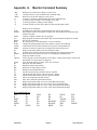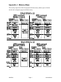
1
8031SDK
Software Development Kit
User's Manual
HiTech Equipment Corporation
9672 Via Excelencia
San Diego, CA 92126
(619) 566-1892
Fax: (619) 530-1458
www.hte.com
[email protected]
8031SDK
Software Development Kit
User’s Manual
Manual
Revision 2.1
December 1998
HiTech Equipment Corporation
9672 Via Excelencia
San Diego, CA 92126
(619) 566-1892
Fax: (619) 530-1458
www.hte.com
[email protected]
© Copyright 1991,1998 by HiTech Equipment Corporation. All rights reserved.
No part of this material may be reproduced, in any form or by any means, without the express
prior written consent of HiTech Equipment Corporation.
THE FINE PRINT
Disclaimer of warranty and limited warranty
HiTech Equipment Corporation has attempted to produce a useful, high quality product at a reasonable price. Every
Development Board unit has been fully tested and checked for quality prior to shipment. It is warranted to be free of defects in
material and workmanship for a period of 90 days after date of purchase. During that time period, HiTech Equipment Corp.
will, at no charge to the purchaser of record, repair or replace any defective unit returned to its Service Department in
accordance with the following instructions:
1.
Phone HiTech Equipment at (619) 566-1892 between 9 am and 3 pm Pacific Time, and obtain a Return Material
Authorization (RMA) number. Do not attempt to return the product without an RMA number.
2.
Provide HiTech Equipment with: Model, Serial Number, Proof of Purchase with date, Return Address, and
preferred return shipping method. Enclose a clear description of the problem experienced and any sample
printouts showing the problem, if possible.
3.
Take proper precautions to protect the product during shipping. Mark the package "FRAGILE", and ship via
UPS, Parcel Post, or Air Freight, insured and prepaid. Be sure the RMA number appears clearly on the box, as
well as any accompanying correspondence. Do not send COLLECT - collect shipments will be refused and
returned to sender.
This warranty is void in cases of misuse, abuse, abnormal conditions of operation, or attempts to alter or modify the function of
the product, or for use within 100 miles of detonation of a nuclear device. The firmware and written material are provided "AS
IS" without warranty of any kind, even if HiTech Equipment Corporation has been advised of that purpose. The entire risk as to
the results and performance of the product is assumed by the user. Also, we do not recommend inserting the board in any
body cavities, as injury may result.
HiTech Equipment Corporation makes no representations or warranties with respect to the contents or use of this product.
HiTech Equipment Corporation shall have no liability or responsibility to purchaser or to any person or entity with respect to any
liability, loss or damage caused or alleged to be caused, directly or indirectly by this product, including but not limited to any
interruption of service, loss of business or anticipatory profits or consequential damage resulting from the use or operation of
this product. This device is not intended for use in life support or life critical equipment. Essentially, if you do something
stupid, don’t blame us; you’re on your own.
HiTech Equipment Corporation reserves the right to make changes to any and all part of this product, at any time, without
obligation to notify any person or entity of such changes and does not represent a commitment on the part of HiTech
Equipment Corporation. So there.
Warranty Registration
Each product is shipped with a unique serial number found on the bottom of the board. Please take a moment to completely fill
out and return the registration card. This will assure prompt service in the unlikely event a problem occurs. If your company
insists on ISO900X certification, please be aware that this only means that we will follow documented procedures no matter
how foolish they may be. Just so you know, our first documented standard procedure following a customer request for ISO
9001 certification is to laugh in your face and double the price.
Trademarks
8031 SDK is a trademark of HiTech Equipment Corporation.
IBM is a registered trademark of International Business Machines Corporation.
IBM PC/XT/AT are trademarks of International Business Machines Corporation.
8031 and 8051 are trademarks of Intel Corporation.
Other trademarks are the property of their owners, whoever they may be.
Table of Contents
INTRODUCTION.................................................................................................................................. 6
FEATURES............................................................................................................................................ 6
SPECIFICATIONS ................................................................................................................................ 8
In Circuit Emulation and External bus expansion.......................................................................... 8
DESIGN CONSIDERATIONS AND LIMITATIONS.......................................................................... 9
GETTING STARTED.......................................................................................................................... 12
EXAMPLE PROGRAM: “HELLO WORLD” .............................................................................................. 14
STEP-BY-STEP INSTRUCTIONS............................................................................................................. 14
USING THE MONITOR ..................................................................................................................... 18
LINE EDITING .................................................................................................................................... 18
START/STOP/RESTART ....................................................................................................................... 19
COMMAND SYNTAX NOTATION................................................................................................... 20
SPECIAL CHARACTERS .................................................................................................................. 20
MONITOR COMMANDS................................................................................................................... 21
? ....................................................................................................................................................... 21
ASM................................................................................................................................................. 21
DASM .............................................................................................................................................. 21
DC.................................................................................................................................................... 21
DI ..................................................................................................................................................... 22
DR.................................................................................................................................................... 22
DX.................................................................................................................................................... 22
EXEC ............................................................................................................................................... 22
FC .................................................................................................................................................... 23
FX .................................................................................................................................................... 23
GO.................................................................................................................................................... 23
HELP................................................................................................................................................ 23
HEX ................................................................................................................................................. 24
INTR ................................................................................................................................................ 24
LOAD............................................................................................................................................... 25
MC ................................................................................................................................................... 25
MEM................................................................................................................................................ 25
MX................................................................................................................................................... 26
PC .................................................................................................................................................... 26
PS..................................................................................................................................................... 26
RESET ............................................................................................................................................. 26
S....................................................................................................................................................... 26
SB .................................................................................................................................................... 27
SC .................................................................................................................................................... 27
SI...................................................................................................................................................... 27
SX .................................................................................................................................................... 28
TRACE............................................................................................................................................. 28
VIEW ............................................................................................................................................... 28
SPECIAL FUNCTION REGISTER NAMES ................................................................................................. 29
DESCRIPTION OF MONITOR OPERATION.................................................................................. 30
DEBUGGING AN INTERRUPT ROUTINE .................................................................................................. 30
INTERRUPT SERVICE VECTORS............................................................................................................ 30
USE OF THE ENHANCED MONITOR BREAKPOINTING FEATURE .............................................................. 30
USING THE SDK AS AN ICE ............................................................................................................ 33
OPERATION OF THE SDK AS AN ICE ................................................................................................... 33
SDK MEMORY MAP IMPLICATIONS FOR ICE OPERATION .................................................................... 34
CIRCUIT DESCRIPTION................................................................................................................... 35
MEMORY MAP PALS.......................................................................................................................... 35
CONFIGURATION JUMPERS .................................................................................................................. 35
SERIAL I/O JUMPERING ...................................................................................................................... 35
MEMORY MAPPING ............................................................................................................................ 36
DEVICE ADDRESS............................................................................................................................... 36
MEMORY SPEEDS ............................................................................................................................... 36
APPENDIX A.
MONITOR COMMAND SUMMARY ....................................................................A
APPENDIX B.
DEVELOPMENT BOARD (SDK) SCHEMATIC...................................................B
APPENDIX C.
OEM SBC SCHEMATIC .........................................................................................C
APPENDIX D.
DEVELOPMENT BOARD JUMPERS....................................................................D
APPENDIX E.
INTEL HEX FORMAT ............................................................................................E
APPENDIX F.
ERROR MESSAGES ................................................................................................ F
Unknown HEX number .................................................................................................................. F
Illegal # of parameters .................................................................................................................. F
No RAM at address : xxxx ............................................................................................................. F
Invalid command........................................................................................................................... F
Unknown error .............................................................................................................................. F
APPENDIX G.
USEFUL MONITOR ROUTINES .......................................................................... G
APPENDIX H.
USING THE OEM VERSION OF THE SBC ........................................................ H
APPENDIX I.
USEFUL WEB SITES.................................................................................................I
APPENDIX J. MEMORY MAPS......................................................................................................... J
APPENDIX K.
PROBLEM REPORT AND COMMENT FORM .................................................. K
Introduction
If you’re anxious to start using the SDK, you can skip ahead to the “Getting
Started” section on PAGE 12 right now!
For those few people who actually read the instructions first, this manual provides
a description of the 8031SDK Software Development Kit, which can operate as an In
Circuit Emulator (ICE) or as an 8031 Single Board Computer (SBC). This manual has
been written for the reader who is familiar with digital logic and microprocessors or
microcontrollers. A specific knowledge of the 8051/8031 family is not assumed, but it
would be advisable for anyone not familiar with this microprocessor family to obtain and
read a description of the 8051 family architecture and instruction set. A large number of
useful documents and sample programs are available from many different web sites, listed
on the HTE website and many others listed in Appendix I.
The term “Development Board” is used throughout this manual for the 8031SDK.
The term 8051 is used throughout this manual to represent the immediate 8051
and derivative processors. The family is derived from the original 8051 and 8052 CPUs
with 4k or 8k of ROM on-chip, the 8031 and 8032 which require off-chip ROM, and the
8751 or 8752 which have 4k or 8k of UV erasable PROM on-chip. Enhancements to the
basic 8051 architecture (such as the 80C552) are not included.
Features
•
•
•
•
•
•
•
•
•
•
•
•
•
•
•
•
Operates as a stand alone single board computer (SBC)
Functions as a simple 8032 In Circuit Emulator (ICE) in External Address mode
Monitor ROM for program development
Connects to COM port of PC or CRT terminal
The on-chip 8051 serial port is available
8032 serial port RS-232 compatible on DB-25 connector
Program download and debug via independent serial link
Help feature displays available commands
Quick program development
User programs stored in static RAM
Includes RAM for user data
Independent serial port used for code development
8032 timers, serial port, and external interrupts available to user
Optional high level language
Disassembly of instruction opcodes
Low cost OEM version for dedicated applications
The Development Board consists of an 8032 microcontroller, user program RAM,
a powerful EPROM-based monitor/debugger that controls emulator operation and the
user serial interface.
8031SDK
Page 6
User's Manual
The Development Board provides the user with the ability to debug code for a
prototype system. The OEM version of the board is usually the target for the final
application. The Development Board has an additional serial port, a monitor ROM and
RAM for program development.
This board doubles as in In Circuit Emulator, using a 40 pin cable and DIP plug to
replace the CPU in the target system. This allows the user to develop code on the SDK in
advance of having a working target board (your hardware design). Later, when the target
board is ready, you simply plug the emulator cable into the target board and run your
programs to debug and test your application.
The Development Board permits reading and writing of system memory, and
control of program execution. The Development Board also allows interactive debugging
of the prototype software and can externally control program execution. The
Development Board's on-board RAM memory permits software debugging without having
to program EPROMs.
It provides powerful functions to assist the designer in the integration, debug and
test phase of 8031SDK hardware/software project development. The Development Board
provides utility commands such as: disassembly, trace, execute to breakpoint, modification
of registers/memories and downloading programs from another computer.
In addition, the Development Board can prove invaluable as an educational tool
for learning the instruction set, since instructions can be executed interactively, and the
effects are immediately apparent on the display.
The user can easily:
• Interpret the results of program activity.
• Disassemble program memory to mnemonics.
• Examine/modify 8032 internal registers/RAM, external memory, or port contents.
In conjunction with any computer capable of running an 8051 assembler, the
Development Board becomes a powerful, stand-alone, program development system. The
board is capable of supporting up to 64k of program memory and 64K of data memory in
two, 28 pin JEDEC sockets. The board also supports two full Asynchronous RS-232
Serial I/O ports. The first is used by the monitor to communicate with the PC. The
second is the serial port built into the 8032 processor.
8031SDK
Page 7
User's Manual
Specifications
CPU
Intel 8032 (or other pin compatible) Microcontroller clocked by an 11.0592 MHz crystal.
This frequency makes it easy to generate standard baud rates using the CPU’s internal
serial port. When used as an ICE, jumpers allow selection of the on-board crystal or the
crytal on the user’s target system. Other crystal values can be used, subject to component
timing constraints, without affecting the serial interface to the Development Board (the
monitor interface uses a separate UART and crystal).
Memory
Two JEDEC 28 pins sockets - 1) Monitor program EPROM and 2) External 32k static
RAM for user programs and data.
Serial I/O Ports
Two serial ports are available on connector P1 (the 8051 internal serial port) and
connector P5 (an external UART). P5 is connected to a ribbon cable with a DB-25 at the
end. The cable on connector P5 is connected to the COM port of a PC running a
communication program, and is used for downloading programs from a PC and debugging
them independent of the 8051’s port. Both ports are RS232 serial. Automatic baud rate
detection is used for the PC connection, and it supports 75 to 38.4k baud, with 7 or 8 data
bits and no parity. Intel Hex down load format. 8032 serial port available as RS-232
serial from second DB-25 connector. A third TTL level serial port is optionally available
when using the Dallas 80C320 controller on connector P3.
Parallel I/O Port
Port 1 of the 8032 is available for user I/O on connector P3.
In Circuit Emulation and External bus expansion
Connector P2 can be used for expansion of the memory and I/O on the board. By using a
40 conductor cable and 40 pin DIP plug, the board can be plugged into the target system’s
8032 compatible socket. Internal or external crystal selectable via jumpers on the board.
Generally, when the board is used in stand-alone mode, Jumpers W1, W2, W8, W9, W10,
and W11 have a jumper plug installed between pins 1 and 2. For use in the ICE mode, the
same jumpers the shorting plugs are installed between pins 2 and 3. See Appendix D for
details. The on-board monitor ROM can download user programs into RAM for
debugging, eliminating the need to program UV or flash EPROM during development.
Power
Requires single +5 volt supply at 100-150 mA typical. Wall mount AC adapter supplied.
Dimensions
6.0 inches by 3.5 inches by 1 inch height.
Environmental
Storage temperature range -25 to +100°C. Operating temperature range 0 to +50°C.
8031SDK
Page 8
User's Manual
Design Considerations and Limitations
If a user program is to be run under the control of the Development Board, care
must be taken to avoid conflicts in the utilization of the Development Board's resources.
A description of the Development Board's use of resources follows:
The Development Board code program address space used for the monitor starts
at 0000h. User program RAM is located starting at 4000h. User programs must be
relocated and assembled starting at 4000h, including interrupt vectors. The interrupt
service vectors are re-mapped to the external RAM with an offset of 4000h. For example,
the external interrupt 0 vector, normally at 0003h is relocated to location 4003h, the
Timer 0 interrupt, normally located at 000Bh is remapped to 400Bh, etc. The
development board also uses External RAM area from FFE0h to FFFFh for the external
RS-232 port. User memory may reside in this area, but cannot be accessed.
All but one of the interrupts have been mapped up to begin at location 4000h (user
RAM space). This is the beginning of user RAM space, and programs should be ORG'd
to begin here. Only the power-up reset interrupt vector has not been mapped into user
RAM space. User interrupt service routines are delayed in the Execute mode, since there
is a code in the monitor ROM which redirects execution to the user program memory
starting at location 4000h.
The Development Board utilizes 128 bytes from 80 (hex) through FF(hex) in the
Internal RAM area of the 8032. In addition, the Development Board requires 8 bytes of
user stack space.
The Development Board uses the one of the interrupts for its trace and breakpoint
facility. The interrupt used by the monitor can be selected with the monitor’s INTR
command. The default interrupt used by the monitor is displayed as part of the sign-on
message displayed when the SDK is first powered up or reset. The corresponding
interrupt enable and priority register bits affecting operation of the selected interrupt
should not be modified, or the single-step and breakpoint features will not work. The
user's program should avoid changing these bits.
The Development Board is configured for expanded (multiplexed address/data
bus) mode (/EA pin grounded). It can be used in the single chip mode only if it is used
with a special version of the CPU, such as the 8052AHBASIC chip. Because of this,
ports P0 and P2 are not available for I/O.
Port bits P3.6 and P3.7 are used for Read and Write lines, and may not be used as discrete
port bits. Clearing either of these bits will disrupt operation of the monitor.
8031SDK
Page 9
User's Manual
Operating the Development Board
Note: This board has MOS devices which can be damaged if exposed to
electrostatic fields and discharges. Grounded conductive workstations and standard
precautions should be used to prevent device damage.
A typical configuration for debugging/development purposes would include:
•
•
•
•
8032 SDK Development Board
RS-232 cable
Dumb terminal or IBM PC/XT/AT with a terminal program.
An 8051 Assembler or Compiler
Serial I/O Connection
The 8051 serial port is available for use in your application, as the PC
communicates with the development board using a separate “PC debug” serial port. This
allows you to develop programs which make use of the 8051’s on chip serial port without
interference with monitor operations. Once your design is complete, the final hardware
can be implemented without the “PC debug” serial port to reduce cost and complexity.
The monitor program communicates with the PC terminal via the second serial
port (not P1 since it is connected to the 8032's on-chip serial port). The second port, used
for connecting to the PC during development is available on connector P5.
The monitor program communicates through the PC debug port on the
Development Board. It will interface to any standard DTE RS-232 asynchronous serial
I/O device set up with 7 or 8 data bits and no parity. The baud rates supported are:
38400
19200
9600
7200
4800
2400
2000
1800
1200
1050
600
300
200
150
134.5
110
75
50
Use of the higher baud rates will usually work, but rates above 9600 may cause
problems with some computers and operating systems, because the PC program may not
be able to keep up with the incoming data rate. If the display of large blocks of data,
such as a memory dump, are uneven or missing characters, reduce the baud rate to 9600
and try again.
The default configuration of the Development Board's serial I/O port is 8 data bits,
1 stop bit, no parity. This will work with most configurations, including those set for 7
data bits. However when a long serial data stream is sent to the Development Board, such
as with the 'Load' command, problems may occur if there is a mismatch in the data bits
setting.
Serial Cable wiring:
DB-25
CRT Terminal Function
2
Receive Data
3
Transmit Data
8031SDK
Page 10
User's Manual
4
5
7
Clear to Send
Ready to Send
Signal Ground
The Development Board does not use hardware or XON/XOFF software
handshake.
The 8032's serial port is made available on the connector mounted on the short
side of the Development Board (P1). The included 11.0592 MHz crystal is chosen to
allow standard baud rates to be generated by the 8032's timers.
8031SDK
Page 11
User's Manual
Getting Started
P5: Connect ribbon cable and to PC COM port
Pin 1, +5V is
not connected
Pin 2, 9V
return, Black
wire from
Power supply
Pin 3, +9VDC,
Black wire with
White stripe
Power Connector P4 - Note proper
orientation of terminal strip!!
P5 Pin 1 goes to
pin 1 (red stripe)
of cable
1) Attach the ribbon cable to the board connector P5. Be careful to orient the ribbon
connector so that pin 1 of the connector is near R2. The female DB-25 connector
should be plugged into the PC’s COM (serial) port. If your PC's COM port has a
9-pin connector, you will need to use a 25 pin (male) to 9 pin (female) adapter.
DO NOT use a null-modem adapter. Your PC should be running a terminal
emulation program, such as PROCOMM or Windows Terminal program.
Win95/98’s Hyperterminal program may also work, but some versions contain
bugs that can be problematic, and it may lose characters on some computers. The
terminal program should initially be set to the COM port (usually COM1 or
COM2) you plugged the board into, 9600 bps, no parity, 8 data bits, and one stop
bit. (9600-N-8-1)
2) Apply power to the Development Board by attaching a power supply to the power
connector. The power connector should be oriented so that the terminal
screws are visible when looking straight down on the board when it is lying
flat. If power is connected properly, the green LED (D1) will light up.
**IMPORTANT!!**
If the power connector is inserted incorrectly the
board WILL BE DAMAGED! Please make sure that the power supply
connection is correct! When using the wall mount power supply, PIN 1 of P4
should NOT be connected to anything.
8031SDK
Page 12
User's Manual
P4 is the power connector on the board. The wall mount power supply must be
connected to pins 2 (9v return/ground/wire with no stripe) and pin 3 (+9 volts/wire
with stripe).
The pins on the power connector are assigned as follows:
Pin
1.
2.
3.
Description
+5v in. This pin is if you already have a regulated +5v supply available.
Ground (to wall mounted 9VDC power supply common).
+6v to +12v in. (to wall mounted 9VDC power supply positive wire.) This
voltage is regulated down to +5v by the on board regulator.
3) Type a Enter to trigger the automatic baud rate detection. The sign on message
"8032 Development Board V x.y", and a prompt (#) will appear on the terminal.
At this prompt, any of the Development Board commands may be entered. Type a
question mark (?) at the prompt for a list of commands.
At this point, you have correctly installed and setup the board with your PC.
The development cycle is usually as follows:
1.
2.
3.
4.
5.
On the PC, edit the program (source file) using an ASCII text editor.
Translate the source file into object (Hex) using an assembler or compiler.
Load the Hex file into SDK program memory with the LOAD command.
Test the program, using breakpoints and single step to find errors.
Edit the source file to correct the errors, and return to step 2 above.
When developing code to be programmed into a non-volatile memory such as Flash or uV
eraseable EPROM, the development cycle is different for step 3. Instead of loading the
program into the SDK’s program RAM, you must load the Hex file into a device
programmer, erase the device, place the device to be programmed into a special
programmer, and program the device. Then turn off the power, remove the SDK monitor
ROM and replace it with your program EPROM. This process takes quite a bit longer
than simply loading a file into the SDK memory, so you will want to wait to program a
device until after you have a working program.
For most of the development process, you will want to download your program from the
PC into the SDK’s program RAM to test it. An example of this process is detailed, using
the “Hello World” program that follows, to demonstrate the development of assembly
language programs on the SDK. This example shows code that will send messages to the
PC’s display, which allows you to see diagnostic and debug information while your
program is executing.
The examples that follow use the shareware Metalink 8051 family assembler to translate
assembly language source code into a Hex object file for downloading to either the SDK
or a device programmer.
8031SDK
Page 13
User's Manual
Example Program: “Hello World”
The following program is a very simple example intended to show how an assembly
program should be written to run on this board. It simply prints the message “Hello
World.” On the display of the PC it is connected to.
;
;
;
;
;
;
Hello world -
8031SBC demo program
Primary controls
$MOD52
; for the 80C32 CPU register definitions etc.
$TITLE(Hello world demo program)
$PAGEWIDTH(132)
;
;
Monitor entry points
;
monitor equ
03F00H
; Go to the monitor
getchar equ
03F03H
; Get character in Acc
sendchar equ
03F06H
; Sends char in Acc to monitor display
sendstr equ
03F09H
; Sends a string to the display
;
; Variable declarations
;
;
base
equ
4000H
; beginning of program RAM on SBC
;
;base
equ
0H
; alternate equate to burn in EPROM
;
reset:
org
base+0H
; reset vector
;
ajmp
start
;
start:
mov
dptr,#message
; point to the string
lcall
sendstr
; print it
lcall
monitor
; show results in regs
jmp
0
; and return
;
;
This is where the data is stored
;
message:
db
0dh, 0ah, 'Hello there!', 0dh, 0ah, '$'
END
NOTE: The program above was written to run with the freeware assembler from
Metalink, both of which are available on the HTE web/ftp site.
ftp://ftp.hte.com/uconline/ecd/51code/
Step-by-Step Instructions
First you must create or edit an 8051 assembly language source file using an unformatted
ASCII text editor, such as Windows Notepad. Next, invoke the assembler at a DOS
prompt and include the source file name after the command. The assembler then translates
8031SDK
Page 14
User's Manual
the 8051 source code into machine code which can be loaded into the SDK board. The
output file should be in Intel hex format (file type .HEX), as documented in Appendix E.
Most 8051 assemblers and compilers generate this type of file. Then you will issue the
LOAD command to the SDK monitor, and use your terminal emulator program on the PC
to send the HEX file to the SDK in ASCII format. Once the program is loaded into the
development board, you can use the monitor Go, Step, and Execute commands to run
your program. Here are the steps to edit and load the “Hello World” program into the
development board and execute the program.
Before you begin, you must have the following files in the default directory (named
C:/51TOOLS in the example below) you will be using to develop your program:
HELLO31.ASM
ASM51.EXE
MOD52
PROCOMM.EXE
The sample program
8051 Assembler program
A file that contains predefined register names & addresses
Procomm or equivalent terminal emulation program
From the DOS prompt you should see something like the following after a directory
command:
C:\51TOOLS>DIR
Volume in drive C is CDRIVE
Directory of C:\51TOOLS
ASM51
EXE
56,453 04-27-90 12:48p ASM51.EXE
HELLO31 ASM
1,047 09-26-98 10:54p HELLO31.ASM
MOD52
3,761 04-27-90 12:44p MOD52
PROCOMM EXE
167,072 12-20-88 9:36a PROCOMM.EXE
4 file(s)
228,333 bytes
2 dir(s)
70,844,416 bytes free
Open the file HELLO31.ASM in Notepad or an equivalent text editor. In order to know
that you have successfully modified the program when you run it, change the line that
reads:
db
0dh, 0ah, 'Hello there!', 0dh, 0ah, '$'
to:
db
0dh, 0ah, 'Hello World!', 0dh, 0ah, '$'
Then save the file as HELLONEW.ASM -- note that this must be a plain, unformatted
ASCII text file, without special embedded formatting characters as would be found in a
word proccessing program document file.
Next, at a DOS prompt, type the Assembler command and file name:
C:/51TOOLS/ASM51 HELLONEW
8051 Cross-Assembler, Version 1.2h
(c) Copyright …
by MetaLink Corporation
First pass
Second pass
ASSEMBLY COMPLETE, 0 ERRORS FOUND
8031SDK
Page 15
User's Manual
In this case, there were no syntax errors detected by the assembler, so you can proceed. If
there had been any errors, you would have to look at the list file (.LST) generated by the
assembler. Then you will have to edit the .ASM file and correct any errors indicated by
the assembler.
Now there will be several new files in the directory:
HELLONEW ASM
HELLONEW HEX
HELLONEW LST
1,047
101
3,098
10-11-98
10-11-98
10-11-98
3:36p HELLONEW.ASM
3:39p HELLONEW.HEX
3:39p HELLONEW.LST
HELLONEW.ASM is the source file we created.
HELLONEW.HEX is the assembled ASCII hex object file we will load in the SDK.
And HELLONEW.LST is assembler list file that contains error and status messages from
the assembler.
Now make sure that the SDK power is off (green LED is off). Then run the terminal
emulation program (we’ll use Procomm for this example):
C:/51TOOLS/PROCOMM
After the startup screen is displayed, push the Enter key until a blue screen appears. If this
is the first time you’ve used Procomm, then type Alt-P and select 9600-N-8-1 (selection
#11). Then select the COM port you are using on your PC (COM1-4 are selections #2023, and press enter). Save your settings by selecting #24 and press enter, so you won’t
need to set them again next time you run Procomm.
Then connect power to the SDK, and press the return key while running Procomm, and
you should see the following sign on message and # prompt:
======================================================
HTE 8031/32 DryICE Monitor
Version 2.6 10/10/90
Copyright (c) 1988,89,90 HiTech Equipment Corporation
======================================================
User Internal RAM from 00h to FFh.
User RAM from 4000h to BE00h.
Single Step Interrupt #5 - Timer 2.
ACC B SP DPTR R0 R1 @R0 @R1 CAFRsOxP Opcode PC
Mnemonic
00 00 07 0000 FF FF FF FF 00000000 FF
4000 MOV
R7,A
#
The # is the command prompt. In this case we want to load the HELLO program hex file,
so we have to tell the monitor we want to load a file, so we use the L command:
#L
After you press the return key, the monitor program waits to receive an Intel ASCII HEX
formatted file, so you must select the file upload function in your terminal emulator to
8031SDK
Page 16
User's Manual
send the ASCII file HELLONEW.HEX to the board. In Procomm, you press the PageUp
key, which opens a menu with several file transfer options, as shown below.
+-----¦ UPLOAD ¦-----+
¦
¦
¦ 1) XMODEM
¦
¦ 2) KERMIT
¦
¦ 3) TELINK
¦
¦ 4) MODEM7
¦
¦ 5) YMODEM
¦
¦ 6) YMODEM BATCH
¦
¦ 7) ASCII
¦
¦ 8) COMPUSERVE B
¦
¦ 9) WXMODEM
¦
¦ 10) YMODEM G
¦
¦ 11) YMODEM G BATCH ¦
¦ ESC Cancel
¦
¦
¦
¦ Protocol: 7
¦
¦
¦
+--------------------+
Select option #7 (ASCII), and when you press Enter, Procomm asks for the name of the
file to upload.
+---¦ ASCII UPLOAD ¦-------------------------------------------+
¦
¦
¦ FILENAME: HELLONEW.HEX
¦
¦
¦
+--------------------------------------------------------------+
If the HEX file is not in the same directory as PROCOMM, you must include the complete
directory path.
Procomm then loads the file into memory, at the default location 4000h, which is where
your program will generally start when running on the development board under the
monitor. When the download operation is complete there is a beeping noise (this is
usually a second or two at most), and you will need to press the Escape key until the
monitor displays the Next Address: XXXX message and the # prompt as shown:
Next Address: 401F
#
The “Next Address” prompt indicates the next available program memory location, which
is the byte following the program we just loaded into program memory. At this point our
program is in memory and ready to run, but just to be sure, we can take a look at the
beginning of the program by using the disassemble command DASM:
#DASM 4000 400B
Opcode PC
Mnemonic
0102
4000 AJMP 4002
90400E 4002 MOV
DPTR,#400E
123F09 4005 LCALL 3F09
123F00 4008 LCALL 3F00
8031SDK
Page 17
User's Manual
020000 400B LJMP
0000
Now let’s try running the program to see if it works:
#G 4000
Hello World!
ß If everything is correct, you should this message.
Congratulations, your program works! If you don’t see this message, check your program
for errors and try again.
After completion, the program re-enters the monitor, which waits for you to press the
Enter key and displays the sign-on message again.
You can also run the program at full speed by using the Execute command:
#E 4000
Hello World!
ACC B SP DPTR R0 R1 @R0 @R1 CAFRsOxP Opcode PC
Mnemonic
24 00 07 401E FF FF FF FF 00000000 020000 400B LJMP 0000
Note there are two differences between the Go and Execute commands:
•
•
The hello message is printed out faster, because the Execute command runs at
full speed but does not allow you to stop the program, unlike the Go
command, which allows the user to stop the program with the Control-C key.
Upon exiting the Go command, the monitor displays the registers.
The differences are covered in the sections on the commands and in the section following
the command descriptions.
Using the Monitor
Line Editing
The Development Board recognizes the use of the Backspace key (<BS>) or the
Delete key (<DEL>) for the correction of errors made during entry of commands. This
echoes as <BS> <space> <BS> to the terminal. The command line will not be read by the
Development Board until it is either terminated by a Carriage Return (<CR>) or exceeds
32 characters. A Control-X will erase the entire input line and restart the input routine.
8031SDK
Page 18
User's Manual
Start/Stop/Restart
For commands producing a large amount of output display, you can type a
Control-S, to stop the scrolling of information on the terminal. Typing any character
(including Control-S), will restart the flow of information. Typing a Control-C will return
the Development Board to the command mode.
8031SDK
Page 19
User's Manual
Command Syntax Notation
The syntax of each command is described with a simple notation system. The
command notation shows what command keywords to use, indicates the parts of the
command that can be omitted or included at the user's option, and shows the places in the
command where the user has a choice of several kinds of entries. The following is used in
command syntax notation:
•
•
•
•
•
•
•
•
•
•
•
Keywords are shown in ALL CAPS.
Parameters are numeric entries and are shown in lower case and entered as
hexadecimal values. Leading zeros are not required.
Required entries are shown without square brackets .
Optional entries are shown in square brackets.
Command and first parameter must be separated by an space.
Parameters must be separated by commas or spaces.
The command is acted on only after you enter a Carriage Return (<CR>) or
exceed 32 characters.
If the starting address is omitted from commands which require a starting address,
it may default to the address immediately past the end of the last command.
If an ending address is not supplied for display commands requiring an ending
address, the the command will output either 8 or 16 lines of information.
Only enough characters to uniquely identify the command need be typed.
Commands can be entered in uppercase, lowercase, or a combination of both.
Special Characters
<BS>
- Backspace key is used for line editing to correct errors.
<CR> - Carriage Return is used to terminated the command string.
<DEL> - Delete key is used for line editing to correct errors.
<ESC> - Escape key is used to abort command executing and return to the
command mode.
^C
- (Control-C) Abort command executing and return to the command mode.
^S
- (Control-S) Stops scrolling of screen display at any time.
^Q
- (Control-Q) Restarts scrolling of screen display.
^X
- (Control-X) Will erase the entire input line and restart the input routine.
8031SDK
Page 20
User's Manual
Monitor Commands
?
Purpose:
Gives list of available commands.
Format:
?
Remarks:
List all available commands to terminal (same as the Help command).
ASM
Purpose:
Assembles mnemonics (instructions) one line at a time into machine
language.
Format:
ASM [start_address]
Remarks:
If start_address is specified, ASM will start from the specified address. If
start_address is not specified, it will start from where the last ASM
command left off. After each line of code is entered, the machine code, the
hexadecimal address, and the code mnemonics will be displayed. ASM will
now prompt for the next line of code. [CR] at the prompt will exit ASM.
If the first character of the line is an '@', it will toggle the disassembly
feature. If the first character of the line is a semicolon (';'), it ignores the
rest of the line.
DASM
Purpose:
Disassembles (translates) program memory into Intel 8051 mnemonics,
their hexadecimal addresses and hexadecimal data. This is not a symbolic
disassembler.
Format:
DASM [start_address] [, end_address]
Remarks:
If start_address is specified, it will start from the specified start address. If
start_address is not specified, it will start from the last disassemble pointer.
If end_address is specified, it will end with the specified end address. If
end_address is not specified, it will disassemble the next 16 instructions.
After the DASM executed, a new disassemble pointer will be saved for the
next DASM.
DC
Purpose:
Dump the contents in bytes of code program memory.
Format:
DC [start_address] [, end_address]
8031SDK
Page 21
User's Manual
Remarks:
If start_address is specified, it will start display from the specified start
address. If start_address is not specified, it will start from the last display
pointer. If end_address is specified, it will end with the specified end
address. If end_address is not specified, it will display 8 lines.
DI
Purpose:
Dump the contents in bytes of internal data memory.
Format:
DI [start_address] [, end_address]
Remarks:
If start_address is specified, it will start display from the specified start
address. If start_address is not specified, it will start from zero. If
end_address is specified, it will end with the specified end address. If
end_address is not specified, it will end at 07Fh.
DR
Purpose:
Dump the contents of all the main registers, and some of the Special
Function Registers (SFR).
Format:
DR
Remarks:
(none).
DX
Purpose:
Dump the contents in bytes of external data memory.
Format:
DX [start_address] [, end_address]
Remarks:
If start_address is specified, it will start display from the specified start
address. If start_address is not specified, it will start from the last display
pointer. If end_address is specified, it will end with the specified end
address. If end_address is not specified, it will display 8 lines.
EXEC
Purpose:
Transfers complete control to the user program. This bypasses the monitor
so the Devlopment Board will not respond to a ^C. Since the Monitor is
disabled, the program will run in real-time.
Format:
EXEC [start_address]
Remarks:
If start_address is specified, it will start execute from the specified start
address. If start_address is not specified, it will start from the present
Program Counter (PC). The monitor must be restarted with a hardware
reset after this command.
8031SDK
Page 22
User's Manual
FC
Purpose:
Fill the code program memory locations with a constant hex value.
Format:
FC start_address , end_address , value
Remarks:
none.
FI
Purpose:
Fill the internal data memory locations with a constant hex value.
Format:
FI start_address , end_address , value
Remarks:
An attempt to fill the upper half of internal data RAM (80h to 0FFh) with a
constant will overwrite the Development Board monitor work space, and may require a
hardware reset to recover.
FX
Purpose:
Fill the external data memory locations with a constant hex value.
Format:
FX start_address , end_address , value
Remarks:
Do not attempt to fill locations FFE0 to FFFF (UART).
GO
Purpose:
Begin program execution and continue until the breakpoint is reached. No
trace history is given.
Format:
GO [start_address] [, breakpoint]
Remarks:
If start_address is specified, it will start execute from the specified start
address. If start_address is not specified, it will start from the present
Program Counter (PC). Breakpoint address must correspond to the
locations of opcodes. If a breakpoint address lies between opcodes, the
monitor will not stop as it passes over the breakpoint location.
Note:
This form of breakpoint will not be recognized inside of an interrupt
routine.
HELP
Purpose:
Gives brief list of available commands and their syntax.
Format:
HELP
Remarks:
List all commands to terminal.
8031SDK
Page 23
User's Manual
HEX
Purpose:
This command allows the operator to do quick hex calculations such as
finding offsets for branch instructions.
Format:
HEX address,offset
Remarks:
The HEX command adds the offset to the address and displays the hex
output. It also subtracts the offset from the address and displays its hex
output.
Display Format: The HEX function displays 4 hex values: the specified address, the
offset, the forward jump address, and the backward jump address.
Example:
#HEX 4AF0,3F
4AF0 003F 4B2F 4AB1
INTR
Purpose:
The monitor requires an interrupt in order to implement single step and
trace debugging functions. By default, the monitor uses one of the
interrupts for single step and break points. The default is shown in the sign
on message, and can be changed using the INTR command. As a result,
the selected interrupt is not available for your use. This command allows
you to change the interrupt used by the monitor. If you need to use that
interrupt, use this command to specify a different interrupt for the monitor
to use.
Format:
INTR [interrupt_number]
Remarks:
The default interrupt varies, depending upon the specific software and
board configuration, and is printed as part of the sign-on message. If you
do not want to use the default, execute the INTR command after each
system reset.
# - Name of Interrupt
0 - External 0
1 - Timer 0
2 - External 1
3 - Timer 1
4 - Serial Port
5 - Timer 2
8031SDK
Page 24
User's Manual
LOAD
Purpose:
Load an absolute Intel Hex file format from the terminal into user program
RAM area.
Format:
Load [offset_address]
Remarks:
Normally the optional address is left out, and the starting address inside the
.HEX file to be loaded specifies the beginning of the program. The device
sending the hex file must be operating at the same baud rate as the
terminal. This is usually done with an upload command to the terminal
emulator of the PC. After the hex file is received, an escape (<ESC>) will
terminate the command and the monitor will report the present location of
the load pointer to the terminal. If 'offset_address' is not specified, offset
will default to zero. If the positional 'offset_address' is specified, it will be
added to the load pointer causing the program to be loaded higher in
memory than was originally intended. The offset 'wraps around' the top of
memory, so it is possible to load a file into a lower location if desired. For
example, an offset of 0FFFE (hex) will cause the file to load 2 locations
lower than origin location. The load command will report an check sum
error, but will not abort the command. NOTE: Data cannot be loaded
between 0000 and 4000h, as that is where the monitor ROM resides.
MC
Purpose:
Moves the contents in a block of the code program memory to a new
location.
Format:
MC start_addr, end_addr, new_addr
Remarks:
Do not try to move a block to a higher memory location within the original
block (overlapping blocks).
MEM
Purpose:
Switch on board RAM between Separate code and external memory with
Overlap code and external memory. Normally, the 8051 is a Harvard
architecture CPU, with separate program and data memory address spaces.
Using this command, you can overlap the program and data memory
spaces, so that the SRAM will respond to either program or data fetch
cycles from the CPU. See Memory Map for details.
Format:
MEM
Remarks:
Toggle memory chip U4 between separate and overlapped program and
external data memory. When overlapped, code and data addresses both
access U4. When separated, the memories must be accessed with MOVC
instructions for getting information from code memory and MOVX
instructions for external data memory.
8031SDK
Page 25
User's Manual
MX
Purpose:
Format:
Moves the contents in a block of the external data memory to a new
location.
MX start_addr, end_addr, new_addr
Remarks:
Do not try to move a block to a higher memory location
located within the original block (overlapping blocks).
PC
Purpose:
Display and alter the contents of the user Program Counter.
Format:
PC [new_value]
Remarks:
If new_value is specified on the command line, it will alter the data in the
user program counter to the new_value. If a new value is not specified on
the command line, it will display the current data in user program counter
and prompt the user with '-'. If new data is typed before the terminating
<CR> then that new data will replace the data currently in user program
counter. If the <CR> is typed with no preceding data then the user
program counter will remain unchanged. On power-up or reset, the
program counter is set to 4000h.
PS
Purpose:
When Program Step is ON, the step command will not display any
instruction code in a CALL routine. This is useful when you don’t want to
see the internal step-by-step operation of a subroutine, and would rather let
the subroutine execute to completion before returning to the monitor.
Format:
PS
Remarks:
The default is off. Typing PS will toggle this option.
RESET
Purpose:
This command clears out all regisisters to the state they would be after a
reset power-up. Refer to the Intel 8051 user manual for details.
Format:
Reset
Remarks:
Reset the registers.
S
Purpose:
Format:
8031SDK
Single step through the program execution beginning at the present
program counter and continue to step until the number of steps has expired
until the breakpoint is reached.
S [number_of_steps]
Page 26
User's Manual
Remarks:
Dumps main register contents and disassembles code memory as it
progresses. If 'number_of_steps' is not specified, it will step only once.
Display:
This command displays register values, then executes the instruction. For
example, after execution of the Step command, the display shows the
accumulator to contain 00h before the instruction is executed. Execution
of a DR command will then show current contents of the registers without
executing an instruction.
#S
ACC
00
#DR
ACC
01
. .
B
00
SP
07
DPTR
0000
R0
35
R1 @R0 @R1
7A 00 00
CAFRs0xP
00000001
Opcode
04
PC Mnemonic
4000 INC
A
B
SP
00 07
.etc.
DPTR
0000
R0
35
R1 @R0 @R1
7A 00 00
CAFRs0xP
00000001
Opcode
04
PC Mnemonic
4001 INC
A
SB
Purpose:
Show the current value of a bit and allows a new value to be substituted if
desired.
Format:
SB bit_address
Remarks:
Only the least significant bit of the data entered will be transferred to the
address bit location.
SC
Purpose:
Show the current value in a byte of code program memory and allows a
new value to be substituted if desired.
Format:
SC address
Remarks:
Pressing <CR> without entering new data will advance the monitor to the
next location without changing memory contents. The entered value will
be written to the address location specified, and will advance the monitor
to the next location. A period must be entered to exit this command.
SI
Purpose:
Show the current value in a byte of internal data memory and allows a new
value to be substituted if desired.
Format:
SI address
Remarks:
Pressing <CR> without entering new data will advance the monitor to the
next location without changing memory contents. The entered value will
be written to the address location specified and will advance the monitor to
the next location. A period must be entered to exit this command.
8031SDK
Page 27
User's Manual
SX
Purpose:
Show the current value in a byte of external data memory and allow a new
value to be substituted if desired.
Format:
SX address
Remarks:
Pressing <CR> without entering new data will advance the monitor to the
next location without changing memory contents. The entered value will
be written to the address location specified, and will advance the monitor
to the next location. A period must be entered to exit this command.
TRACE
Purpose:
Begin program execution and continue until the breakpoint is reached.
Dumps main register contents and disassembly of code memory as it
progresses.
Format:
TRACE [start_address] [, breakpoint]
Remarks:
If start_address is specified, it will start to execute from the specified start
address. If start_address is not specified, it will start from the present
Program Counter (PC). Breakpoint address must correspond to the
locations of opcodes. If a breakpoint address lies between opcodes, the
monitor will not stop as it passes over the breakpoint location.
Note:
This form of breakpoint will not be recognized inside of an interrupt
routine.
Display:
See 'S' command for detail.
VIEW
Purpose:
This command allows you to see when your interrupts are occuring during
the execution of your code in the Trace mode. The interrupts are also
shown during the GO and STEP commands. Typing "View" will toggle
the view option on and off.
Format:
View
Remarks:
The default for view is off
8031SDK
Page 28
User's Manual
Special Function Register Names
There are command keyword registers. If new_value is specified on the command
line, it will alter the data in the user keyword register to the new_value. If a new value is
not specified on the command line, it will display the current data in user keyword register
and prompt the user with a # sign. If new data is typed before the terminating Enter key
then the new data will replace the data currently in user keyword register. If the Enter key
is typed with no preceding data then the user keyword register will be unchanged. The
keyword registers are as follows:
ACC
B
DPH
DPL
DPTR
IE
Register
ACC*
B*
DPTR*
DPL*
DPH*
IE*
IP
P0
P1
P2
P3
PCON
PSW*
RCAP2H+
RCAP2L+
SBUF
SCON
SP*
T2CON+
TCON
TH0
TL0
TH1
TL1
TH2+
TL2+
TMOD
IP
PSW
R5
P0
R0
R6
P1
R1
R7
P2
R2
RCAP2H
P3
R3
RCAP2L
PCON
R4
SBUF
Name
Accumulator
B register
Data Pointer
Data Pointer low byte
Data Pointer high byte
Interrupt Enable Control
Interrupt Priority Control
Port 0
Port 1
Port 2
Port 3
Power Control
Program Status Word
T/C 2 Capture high byte
T/C 2 Capture low byte
Serial Data Buffer
Serial Control
Stack Pointer
Timer/Counter 2 Control
Timer/Counter Control
Timer/Counter 0 high byte
Timer/Counter 0 low byte
Timer/Counter 1 high byte
Timer/Counter 1 low byte
Timer/Counter 2 high byte
Timer/Counter 2 low byte
Timer/Counter Mode Control
SCON
SP
T2CON
TCON
TH0
TL0
TH1
TL1
TH2
TL2
TMOD
Address
0E0h
0F0h
<n/a>
081h
082h
0A8h
0B8h
080h
090h
0A0h
0B0h
087h
0D0h
0CBh
0CAh
099h
098h
080h
0C8h
088h
08Ch
08Ah
08Dh
08Bh
0CDh
0CCh
089h
* These registers are stored in memory as "user image" during monitor operation.
+These registers are only for the 8032/8052.
8031SDK
Page 29
User's Manual
Description of Monitor Operation
Debugging an interrupt routine
The Development Board's trace and breakpoint functions are interrupt driven.
That is, an interrupt is generated between each instruction causing the monitor to
temporarily take control of the program. The trace information is sent to the console
and/or the breakpoint comparison is made. For this reason, the trace and breakpoint
features are normally disabled inside of interrupt routines. Usually the results of interrupts
can be seen from within the main body of the program, through altered registers, memory
locations, etc. This can be observed by running the sample interrupt program provided in
the appendix. When debugging an interrupt routine, the best approach is to trace the
operation of the routine as a stand-alone module by transferring program control directly
to it from the monitor.
Interrupt Service Vectors
All but two of the interrupts have been mapped up to begin at location 4000h (user
RAM space). This is the beginning of user RAM space, and programs should be ORG'd
to begin here. Only the power-up reset and timer 2 interrupt vectors have not been
mapped into user RAM space. A typical source program might begin as follows:
USERRAM
EQU
4000h
ORG
USERRAM+00h
JMP
start_program
ORG
USERRAM+03h
JMP
int_0_routine
ORG
USERRAM+0Bh
JMP
timer_0_routine
;jump to the beginning of program
;jump to external 0 interrupt service routine
;jump to timer 0 interrupt service routine
etc . . .
With this type of organization, once a program has been debugged it may be
ROM'd by simply changing the EQU of 'USERRAM' to 0 and reassembling.
Use of the Enhanced Monitor Breakpointing Feature
The following is a description of how the breakpoint feature has been implemented in the
monitor firmware. This allows the user of the Development boards to take full advantage
of this feature.
When a breakpoint address is specified, that address location as well as the next two
addresses are filled with a LJMP monitor instruction (a 3 byte instruction). When the
8031SDK
Page 30
User's Manual
program executes that jump instruction, control is returned to the monitor, which restores
the user's code to the breakpoint address, and adjusts the program counter to point to it.
Implementing a breakpoint function in firmware this way allows the creation of very
inexpensive development tools like this SDK, but the user must be aware of a few
anomalies that can occur when he is debugging his code. These anomalies involve the
careful selection of breakpoint addresses, and manifest themselves as improper user
program executions or crashes.
1. As mentioned above, the code at the breakpoint address is replaced with a 3 byte jump
instruction. If you set a breakpoint within 2 instructions of the end of a subroutine, or
where some other program entry point occurs, the program will likely crash. See example
below:
....
MOV
A,R5
;SETTING A BREAKPOINT HERE OR THE
RET
;NEXT INSTRUCTION WILL CORRUPT THE
TIMER0:
PUSH
PSW
;FIRST INSTRUCTION OF THE TIMER
PUSH
A
;INTERRUPT ROUTINE.
....
A breakpoint set at the first or second instruction shown will corrupt the first instruction
of the timer interrupt, causing an extra POP of the PSW (which never got pushed),
eventually causing the stack to go below it's limits, and crashing the program.
2. If the background routine is very short, and the major processing is done in interrupt
foreground routines, there is a problem which could result from setting a breakpoint in the
interrupt routine, followed by a breakpoint in the background routine. The shorter the
background routine is, the better the chance is that the interrupt return address is in the
middle of the breakpoint you set. The following is a repeat of the sequence for clarity:
a.) Start the program and set a breakpoint at the end of an interrupt routine:
#E ,YYYY
Main program:
Interrupt Service Routine
Main:
INT0:
ZZZ:
....
....
MOV ...
MOV ...
ADD ...
....
YYYY:
....
MOV ....
DJNZ ...
....
b.) After reaching breakpoint YYYY, execute to a breakpoint within the Main module:
#E ,ZZZZ
c.) If the interrupt return address on the stack is ZZZZ+1 or ZZZZ+2, the program will
crash.
d.) The probability of this occurring goes up as the size of the Main program loop goes
down. Consider the case of:
8031SDK
Page 31
User's Manual
Main:
MOV
SJMP
A,#5
Main
;2 bytes
;2 bytes
A breakpoint set at Main will mess up the next instruction as well. If the next instruction
is at the interrupt return address, the program crashes. This will happen 50% of the time.
By carefully selecting your breakpoints to avoid these pitfalls, you can make full and
proper use of the features of the monitor.
8031SDK
Page 32
User's Manual
Using the SDK as an ICE
The SDK may be used as an ICE (In-Circuit Emulator) for 8051 compatible CPUs,
running in the external program access (external bus) mode. The “host” system is your
PC, which is used to communicate with and control the SDK. The “target” system is an
8051 system of your own design, which will incorporate an 8051 style CPU and operate
independently of the SDK once you have it running properly. One end of the ICE cable
plugs into the P2 connector underneath the SDK, and the other end has a 40 pin DIP plug,
which can be plugged into the target system in place of the CPU chip. Then the SDK can
be used to develop and debug your programs in the target system, by loading your
program into the SDK’s program RAM.
Operation of the SDK as an ICE
The SDK can be operated as an ICE, by plugging the ICE cable into P2 on the
bottom of the SDK board, and the DIP plug into your target system where the 8051
would have been installed. The ICE cable is shown below, installed on the P2 connector
that is on the bottom of the SDK board. Be sure to check the orientation and alignment of
the cable, to prevent damage to the SDK or your target system.
DIP plug to
be inserted
in target
system CPU
socket
Pin 1 (red
stripe) cable
installed near
edge of board
ICE Cable attached to underside of SDK
There are also jumpers which should generally be moved for ICE operation. They
are W1 and W2, which select the crystal on the SDK or the target system’s crystal for
clocking the CPU chip. The photo below shows how the ICE cable is plugged into a
target system’s CPU socket. In the photo, the ICE cable is plugged into another SDK
board’s CPU socket. It almost looks like a case of recursion in hardware, but you can’t
plug an SDK’s cable into itself!
SDK ICE cable plugged into target CPU socket
8031SDK
Page 33
User's Manual
SDK Memory Map Implications for ICE Operation
When the SDK is plugged into the target system, the memory and I/O devices on
the SDK will take precedence to those on the target system and overlay them. In other
words, the monitor ROM will occupy the program memory space from 0000 to 4000h,
and any memory in that range that exists in your target system will be ignored by the SDK.
Likewise the RAM at locations 4000h – BDFFh and I/O in the external data memory
address space at locations FFE0h to FFFFh on the SDK will preempt use of these
locations in your target system. (These addresses assume the standard 32Kx8 SRAM is
installed in U4. See memory maps appendix J for details.)
Memory cycles which access resources on the SDK will not access memory
location in the target system via the ICE cable. Only accesses to memory addresses which
are not implemented on the SDK will access the target system addresses. When a user
program is executed in the default memory configuration (MEM command, separate
mode), it will access program memory on the SDK from 0000h to BDFFh and on the
target CPU in the range C000h to FFDFh. When the program accesses external data
memory, it will access data memory on the target system in the range 0000h to FFDFh,
and the reserved monitor memory mapped I/O on the SDK in the range FFE0h to FFFFh.
When the user program is executed in overlapped memory mode (MEM command,
overlap mode), the user program memory (SRAM U4) will also appear in external data
memory in the range 4000h to C000h.
8031SDK
Page 34
User's Manual
Circuit Description
The processor is the 8032, the ROMless version of the 8052 family. It has four, 8
bit I/O ports, P0 thru P3. P0 is used as the data port and also carries the low order eight
address bits. These bits are latched by the octal latch on the falling edge of the ALE line.
These are then combined with the high order address bits from P2 to form the full 16 bit
address. The address decoders are PLD's, which decode the three most significant address
lines to deliver the chip select and read signals to the external RAM and ROM. This
decoder provides several different combinations of mapping which are discussed in the
section on jumpering. The PLD's multiplex other I/O port lines as well.
Memory Map PALs
Two 16V8 PLDs are programmed to provide address mapping for Static RAM
types of 8k and 32k on board and off board. Other mapping may be incorporated by
contacting HiTech Equipment for your custom programming needs.
Configuration Jumpers
The Development Board is shipped with the default jumpers installed as shown in
Appendix D.
The jumpers on the Development Board are classified into three groups. Serial
I/O, Memory device selection, and Memory mapping. The memory mapping group is
further broken down into two sub-groups; device address, and address field. Address field
refers to program memory space versus Data memory space.
Serial I/O Jumpering
The default jumper installation for the serial I/O port is with all modem control
lines disabled. Incoming DTR and RTS are ignored and the outgoing CTS and DSR are
tied high (+12v.). This will allow the Development Board to send to and receive from
most standard RS-232 "terminal" devices. Note that the Development Board is
configured as an RS-232 DCE (like a "modem"), and that a null modem is not required to
communicate with a standard PC COM port.
The monitor does not utilize any of the modem control lines.
8031SDK
Page 35
User's Manual
Memory Mapping
The 8051 family of processors are capable of addressing a maximum of 128k of
external program and data memory. This memory is broken down into two types, with the
processor being able to address maximum of 64k of program memory (read only), and a
maximum of 64k of data or read/write memory. (Peripheral devices are also usually
located in the latter space). Both memory fields are addressed using the same 16 address
lines. During a read, the desired field is selected by the use of the RD (for data memory)
or the PSEN (for program memory)lines.
The Development Board has a jumper field associated with each memory socket to
allow the location of that device in either external RAM space, program memory space, or
both. In the last option, the device will appear at the same address in both spaces. This
option is required for operation of the monitor during program development or in any
operation which requires having the CPU write into it's own program memory space. This
limits the system to a total of 64k of memory but once program development is done, the
Development Board can be jumpered for its full 128k range.
Device Address
The Development Board is set up to support the development monitor EPROM in
U3 and 32k Static RAM devices in location U4. These may be changed by alteration of
the jumpers as shown in the schematic. See Appendix D for more details.
Memory Speeds
Two important memory timing specifications must be met when adding memory
devices to the Development Board. The most common timing consideration when
selecting memory devices in their response time from receiving a chip select and valid
address to their placing data on the bus. (Note that the times required by the 8051 differ
depending on whether the read is from data or program memory, see the 8051 Data
Sheet). The other timing specification which must be considered, is the time required by
the device before it releases the bus after it is deselected. For the program memory, this
must be less than 75 ns. at 11.059 Mhz. These times depend on the specific 8051 CPU
variant used, and the memory and logic devices.
More information and application note references are available on the subject of
timing, and can be found on the HTE web site, and in the text "Embedded Controller
Design" by Ken Arnold.
8031SDK
Page 36
User's Manual
Appendix A.
Monitor Command Summary
<BS>
<CR>
<DEL>
^C
^S
^Q
^X
Backspace key used for line editing to correct errors.
Carriage Return is used to terminated the command string.
Delete key used for line editing to correct errors.
(Control-C) Abort the command and return to the command mode.
(Control-S) Stops scrolling of screen display at any time.
(Control-Q) Restarts scrolling of screen display.
(Control-X) Will erase the entire input line and restart the input routine.
?
ASM
DASM
Displays list of commands.
Assembles 8051 mnemonics and hexadecimal into memory from address
Disassembles memory from address to address into 8051 mnemonics and hexadecimal
addresses and data.
Transfers complete control to the user program.
Begin program execution at start address and continue until the breakpoint is reached.
Gives list of commands.
Hex calculator, gives sum & difference of two hex numbers.
Changes the debug interrupt used by the monitor to the specified interrupt.
Load an Intel Hex file format from the serial port into external RAM area.
Switches U4 between separate and overlapped code and external access.
Display and permits modify of the user Program Counter.
Switches between tracing subroutine calls and skipping over them in Step mode.
Restores the processor to the same state as activating the CPU RESET pin.
Single step number of steps.
Traces program execution beginning at start address. Dumps main register contents and
disassembly of code memory as it progresses.
View interrupts during executing. Turn view off and on.
Dumps the code data memory.
Dumps the internal data memory.
Dumps the on-chip register memory.
Dumps the external data memory.
Fill the code data memory with user specific constant.
Fill the internal data memory with user specific constant.
Fill the external data memory with user specific constant.
Move bytes within the code data memory.
Move bytes within the external data memory.
Display and permits modify of a series of bit addressable memory.
Display and permits modify of a series of byte from code data memory.
Display and permits modify of a series of byte from internal data memory.
Display and permits modify of a series of byte from external data memory.
EXEC
GO
HELP
HEX
INTR
LOAD
MEM
PC
PS
RESET
S
TRACE
VIEW
DC
DI
DR
DX
FC
FI
FX
MC
MX
SB
SC
SI
SX
Keyword Registers:
ACC
IP
B
P0
DPH
P1
DPL
P2
DPTR
P3
IE
PCON
8031SDK
PSW
R0
R1
R2
R3
R4
R5
R6
R7
RCAP2H
RCAP2L
SBUF
Page A
SCON
SP
T2CON
TCON
TH0
TL0
TH1
TL1
TH2
TL2
TMOD
User's Manual
Appendix B.
8031SDK
Development Board (SDK) Schematic
Page B
User's Manual
Appendix C.
8031SDK
OEM SBC Schematic
Page C
User's Manual
Appendix D.
Development Board Jumpers
Jumper Pins
Name Shorted
Function
W1
W2
1-2
1-2
External crystal - X1
External crystal - X2
W1
W2
2-3
2-3
W3
1-2
W3
2-3
W4
1-2
W4
2-3
W5
1-2
W5
2-3
U1 /EA to +5v- CPU internal program access mode
W6
out
8 k Static RAM installed
W6
in
32 k Static RAM installed
W7
out
Normal
W7
in
U1 - Reset
W8
W8
W8
W8
1-2
3-4
5-6
7-8
W8
W8
W8
W8
1-4
2-3
5-8
6-7
*
*
On Board crystal - X1
On Board crystal - X2
*
U4 - 8k Static RAM
U4 - 32k Static RAM
*
U3 - 2764/27128 EPROM
U3 - 27256 EPROM
*
*
*
*
*
U1 /EA to ground – CPU external program access mode
DCE configuration
DTE configuration
* Note: Asterisk (*) means the default jumper has been cut (a trace) on the bottom side of
the board. Normally, the traces are cut prior to being shipped, and jumper plugs are
installed.
8031SDK
Page D
User's Manual
Appendix E.
Intel Hex Format
Intel hex data file formats begin with a 9-character prefix and end with a 2character suffix. The byte count must be equal to the number of data bytes in the record.
Data record and end-of-file record are the two types of records. The number of bytes per
record is variable. Each record begins with a colon, which is followed by a 2-character
byte count. The 4 characters following the byte count is the address of the first data byte.
Each byte is represented by 2 hex digits that equals to the number of bytes in each record.
It ends with the checksum.
:BCAAAATTHH . . . HHCC
:
Start character (colon)
BC
The hexadecimal number of bytes in the record. If BC = 0 the it is the end-offile record.
AAAA
Address in hexadecimal of first data byte in the record.
TT
Record type.
If TT = 00 then data record.
If TT = 01 then end-of-file record
HH
One data byte in hexadecimal notation.
CC
Checksum is the two's complement of binary summation of preceding bytes in
record including the byte count, address and record type.
8031SDK
Page E
User's Manual
Appendix F.
Error Messages
Unknown HEX number
Explanation: This error is caused by an invalid hex number. All parameters are
entered in hexadecimal.
Action:
Enter a valid hexadecimal number.
Illegal # of parameters
Explanation: This error occurs when the command needs more parameters.
Action:
Check the command description for the command.
No RAM at address : xxxx
Explanation: This error occurs at address 'xxxx' when a command failed to verify
after it has written a byte to RAM.
Action:
Check the hardware for RAM at .'xxxx'.
Invalid command
Explanation: An invalid command was detected.
Action:
Correct the invalid command.
Unknown error
Explanation: An unknown error was detected. This was probably caused by
writing to the monitor internal RAM area.
Action:
8031SDK
Reset the system.
Page F
User's Manual
Appendix G.
Useful Monitor Routines
You can use the development board for purposes other than code development. Below
are the entry points to the subroutines in our firmware which might be useful. These
routines for ASCII characters from the host via the external RS-232 port (P5).
Routine
Entry point
Description
Getchar
3F03H
;Returns character in acc
;Will not return until character
;has been received. May or may
;not echo character.
;No other registers are affected.
Sendchar
3F06H
;Sends character in acc.
;No other registers are affected.
Sendstr
3F09H
;
;
;
;
8031SDK
Sends a string to the display.
String is in External memory
DP points to string
Terminate string with $ character
Page G
User's Manual
Appendix H.
Using the OEM version of the SBC
Essentially, the OEM (Original Equipment Manufacturer) version of the SBC is a
minimum configuration version of the Development Board. This version is a much lower
cost unit (<$50.00US), as it does not have the components which are only needed for
development of programs. It does not have the following items:
1. A monitor EPROM. On the SBC, the user's final program is burned into an EPROM
and put in the same socket where the monitor EPROM is on the Development Board
(U3).
2. An external serial port. On the SBC, only one DB-25 connector is present. The
8032's serial port is available at RS-232 levels at the DB-25 connector on the short
side of the board. The extra serial port present on the Development Board is not
needed since code is not developed on the SBC. The extra serial port is available as
an option, however.
3. The decoding PALs. These are used in the Development Board to decode the
addresses used by the UART and to map RAM and EPROM in the 8032's address
space. The SBC does not need memory decoding so these connections must be
jumpered as follows:
For U5, Connect:
a. pins 5 and 16
b. pins 8 and 14
c. pins 9 and 13
For U6, Connect:
a. pins 9 and 19
b. pins 13 and 20
Once code development has been completed on the Development Board, it is
ready to be programmed into an EPROM and installed in SBCs. In order to do this,
though, the program must first be assembled with its origin starting at 0000h. If the
program has been written as shown in the section on Interrupt Service Vectors, then this is
simply a matter of changing the USERRAM equate to 0000h. After the program has been
reassembled, it is ready to be programmed into an EPROM and run in the SBC.
In addition, the code can be contained in an 8051 variant that has internal memory,
such as the 8051 BASIC chip. In this case, the processor must be told to execute code
internally. This is done by cutting the trace shorting pins 1 and 2 of jumper 3 and
installing a jumper connector on pins 2 and 3.
The following is the pinout for the power connector:
Pin Description
1. +5v in. This pin is used instead of pin 1 if you already have a regulated +5v
supply available. However, if there is no on-board regulator, this pin must be
used to deliver power to the board.
2. Ground
3. If a voltage regulator is installed in U9, +6v to +12v may be applied to this pin.
This voltage is regulated down to +5v by U9.
8031SDK
Page H
User's Manual
Appendix I.
Useful Web sites
Below is a list of useful web sites, related to the
8051 family of devices.
http://www.hte.com
The HTE web site has lots of useful information, updates,
free/shareware, the current version of this manual, and
links to all the sites listed below, plus new and updated
information.
http://developer.intel.com
Intel is the originator of the 8051 architecture, and has
free software utilities that allow automatic configuration
of the various 8051 on-chip resources.
http://mcu.philips.com
Philips Semiconductors has an extensive line of 8051
derivatives and a large collection of application notes on
their web page.
http://www.atmel.com
Atmel has 8051 derivatives that incorporate flash program
memory and are available in packages as small as 20 pins.
8031SDK
Page I
User's Manual
Appendix J. Memory Maps
The memory maps below show the program and data memory address spaces for both
normal and overlapped program and data memory.
8031SDK
Page J
User's Manual
Appendix K.
Problem Report and Comment Form
Please complete this form if you discover any software
or hardware problems, documentation problems, or would like
to suggest product enhancements. Duplicate this form if you
need additional copies and/or attach extra pages if
necessary.
___ Hardware Problem
___ Software Problem
___ Documentation Problem
___ Product Enhancement
Date: ________________________
Serial #: ______________
Product: ______________________
Version #: ____________
Name: ___________________________ Title: _____________
Company: _________________________________________
City: ________________________ State: _____ Zip: ________
Country: _____________________
Phone: (______) ____________________
Ext: ____________
Please describe the problem, how to reproduce it and your
suggested correction. Or, decscribe documention problems or
suggest enhancements that you would like to see added to
this product.
Send or fax form to:
HiTech Equipment Corporation Attn: Technical Support
9672 Via Excelencia
(619) 566-1892
San Diego, CA 92126
Fax: (619) 530-1458
http://www.hte.com
Or e-mail [email protected]
8031SDK
Page K
User's Manual