1
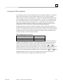
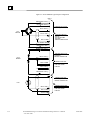
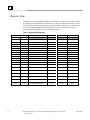
GE Fanuc Automation Programmable Control Products IC697VRD008 Intelligent 8-Channel RTD/Strain Bridge Board User’s Manual GFK-2098 514-000449-000 A December 2001 GFL-002 Warnings, Cautions, and Notes as Used in this Publication Warning Warning notices are used in this publication to emphasize that hazardous voltages, currents, temperatures, or other conditions that could cause personal injury exist in this equipment or may be associated with its use. In situations where inattention could cause either personal injury or damage to equipment, a Warning notice is used. Caution Caution notices are used where equipment might be damaged if care is not taken. Note Notes merely call attention to information that is especially significant to understanding and operating the equipment. This document is based on information available at the time of its publication. While efforts have been made to be accurate, the information contained herein does not purport to cover all details or variations in hardware or software, nor to provide for every possible contingency in connection with installation, operation, or maintenance. Features may be described herein which are not present in all hardware and software systems. GE Fanuc Automation assumes no obligation of notice to holders of this document with respect to changes subsequently made. GE Fanuc Automation makes no representation or warranty, expressed, implied, or statutory with respect to, and assumes no responsibility for the accuracy, completeness, sufficiency, or usefulness of the information contained herein. No warranties of merchantability or fitness for purpose shall apply. The following are trademarks of GE Fanuc Automation North America, Inc. Alarm Master CIMPLICITY CIMPLICITY 90–ADS CIMSTAR Field Control GEnet Genius Helpmate Logicmaster Modelmaster Motion Mate ProLoop PROMACRO PowerMotion PowerTRAC Series 90 Series Five Series One ©Copyright 2001 GE Fanuc Automation North America, Inc. All Rights Reserved Series Six Series Three VersaMax VersaPro VuMaster Workmaster Contents Chapter 1 Introduction, Description, and Specifications ......................................... 1-1 Reference Material and Other GE Fanuc Manuals................................................... 1-1 Features .................................................................................................................... 1-2 Applications ............................................................................................................. 1-3 Safety Summary ....................................................................................................... 1-5 Chapter 2 Configuration and Installation.................................................................. 2-1 Unpacking Procedures ............................................................................................. 2-2 Physical Installation ................................................................................................. 2-3 Before Applying Power: Checklist .......................................................................... 2-4 Operational Configuration ....................................................................................... 2-5 Calibration.............................................................................................................. 2-10 Connector Descriptions .......................................................................................... 2-13 Chapter 3 Programming.............................................................................................. 3-1 Register Map ............................................................................................................ 3-2 Board Address and Access Mode............................................................................. 3-3 Board Initialization................................................................................................... 3-4 Board Identification Register ................................................................................... 3-5 Control and Status Register (CSR)........................................................................... 3-6 Self-Test/Error Register ........................................................................................... 3-9 Sequence Initiation and Monitoring ....................................................................... 3-11 Channel Control Register (CCR) ........................................................................... 3-12 Response Select Register (RSR) ............................................................................ 3-15 Converted Channel Data Registers (CCDs) ........................................................... 3-16 Processing Sequence .............................................................................................. 3-17 Operating Modes.................................................................................................... 3-19 Strain Bridge Excitation ......................................................................................... 3-20 Program Examples ................................................................................................. 3-21 Chapter 4 Theory of Operation .................................................................................. 4-1 Operational Overview .............................................................................................. 4-2 VMEbus Control Interface ....................................................................................... 4-3 Controller and Processor .......................................................................................... 4-5 Input Signal Conditioning ........................................................................................ 4-6 Sensor Excitation ..................................................................................................... 4-8 Multiplexing and Digitizing ..................................................................................... 4-9 GFK-2098 iii Contents Signal Processing ................................................................................................... 4-10 Built-In Power Converter ....................................................................................... 4-11 Maintenance ....................................................................................................... 5-1 iv IC697VRD008 Intelligent 8-Channel RTD/Strain Bridge Board User’s Manual – December 2001 GFK-2098 Chapter Introduction, Description, and Specifications 1 This manual describes the installation and operation of the IC697VRD008 Intelligent 8-Channel RTD/Strain Bridge Board. Reference Material and Other GE Fanuc Manuals For a detailed explanation of the VMEbus and its characteristics, “The VMEbus Specification” is available from: VITA VMEbus International Trade Association 7825 East Gelding Dr., No. 104 Scottsdale, AZ 85260 (480) 951-8866 FAX: (480) 951-0720 Internet: www.vita.com GFK-2098 1-1 1 Features The Bridge Board is an intelligent, 8-channel, low-level input board, designed specifically for use with either strain bridge or RTD inputs. The board is self-contained, and provides all necessary signal conditioning, multiplexing, digitizing, and digital signal processing. A 16-bit on-board processor controls all board functions and performs all necessary signal processing. The Bridge Board can be configured for both strain bridge and RTD inputs simultaneously. Strain bridge and RTD inputs are received through the front panel P3 connector. An on-board Analog-toDigital Converter (ADC) digitizes each input signal into a 12-bit plus sign data word which is processed digitally to produce the final output data. The board provides linearization for two RTD types, and supplies individual constant current excitation for each RTD channel. Strain bridge excitation is provided from an on-board supply. All inputs are protected against both normal mode and common-mode overvoltages. The following brief overview of principal features illustrates the flexibility and performance that is available with the Bridge Board: 1-2 • Eight differential input channels • Linearization for RTD inputs • RTD excitation and lead wire compensation standard • Strain gage bridge excitation supply • On-board 16-bit microcomputer • Dual-port data registers for minimum host overhead • Common-mode rejection: 70 dB at 60 Hz • Nonvolatile storage of calibration parameters eliminates offset and gain potentiometers • Analog-to-Digital Converter (ADC) 12 bits plus sign • Accepts full- and half-bridge inputs • All inputs protected to 130 Vrms • Powerup and Reset self-test IC697VRD008 Intelligent 8-Channel RTD/Strain Bridge Board User’s Manual – December 2001 GFK-2098 1 Applications The broad range of system applications that can benefit from the Bridge Board’s capabilities include: GFK-2098 • Temperature measurement • Strain measurement • Pressure and load measurement • Precision low-level analog inputs • Industrial control systems • Machinery instrumentation • Low-level data acquisition Chapter 1 Introduction, Description, and Specifications 1-3 1 Figure 1-1: IC697VRD008 8-Channel Strain/RTD Board Block Diagram VOLTAGE REFERENCE FRONT PANEL CONNECTOR (USER I/O PINS) P3 -10.00 VDC BRIDGE EXCITATION STRAIN BRIDGE +5 V, +10 V at 190 mA EXCITATION SUPPLY ±10 V FSR BRIDGE SENSE CH0 13 ANALOG MUX RTD EXCITATION EIGHT STRAIN BRIDGE OR RTD INPUT CHANNELS ADC 12-bit PLUS SIGN DIFFERENTIAL SIGNAL CONDITIONERS (8) AND MULTIPLEXER CHANNEL 0 INPUT CH7 CHANNEL MUX NODE CHANNEL 7 INPUT CHANNEL SELECT EXTERNAL SYNC (TTL) CONTROL AND LINEARIZATION PROCESSOR PROCESSING MODE VMEbus P1 INTERNAL CPU BUS 3 VMEbus COMPATIBILITY INTERFACE SEQUENCE COMPLETE IDB 00 TO 15 16 POWER CONTROL AND STATUS REGISTER (CSR) START SEQUENCE TRI-STATE DATA BUFFER PDB00 TO PDB15 CONVERTER 1-4 16 IC697VRD008 Intelligent 8-Channel RTD/Strain Bridge Board User’s Manual – December 2001 16 GFK-2098 1 Safety Summary Warning The following general safety precautions must be observed during all phases of this operation, service, and repair of this product. Failure to comply with these precautions or with specific warnings elsewhere in this manual violates safety standards of design, manufacture, and intended use of this product. GE Fanuc assumes no liability for the customer’s failure to comply with these requirements. Ground the System To minimize shock hazard, the chassis and system cabinet must be connected to an electrical ground. A three-conductor AC power cable should be used. The power cable must either be plugged into an approved three-contact electrical outlet or used with a three-contact to two-contact adapter with the grounding wire (green) firmly connected to an electrical ground (safety ground) at the power outlet. Do Not Operate in an Explosive Atmosphere Do not operate the system in the presence of flammable gases or fumes. Operation of any electrical system in such an environment constitutes a definite safety hazard. Keep Away from Live Circuits Operating personnel must not remove product covers. Component replacement and internal adjustments must be made by qualified maintenance personnel. Do not replace components with power cable connected. Under certain conditions, dangerous voltages may exist even with the power cable removed. To avoid injuries, always disconnect power and discharge circuits before touching them. Do Not Service or Adjust Alone Do not attempt internal service or adjustment unless another person, capable of rendering first aid and resuscitation, is present. Do Not Substitute Parts or Modify System Because of the danger of introducing additional hazards, do not install substitute parts or perform any unauthorized modification to the product. Return the product to GE Fanuc for service and repair to ensure that safety features are maintained. GFK-2098 Chapter 1 Introduction, Description, and Specifications 1-5 Chapter Configuration and Installation 2 This chapter contains configuration and installation instructions for the Bridge Board, and is divided into the following sections: GFK-2098 Unpacking Procedure Physical Installation Before Applying Power: Checklist Operational Configuration Calibration Connector Descriptions 2-1 2 Unpacking Procedures Caution Some of the components assembled on GE Fanuc products can be sensitive to electrostatic discharge and damage can occur on boards that are subjected to a high-energy electrostatic field. When the board is placed on a bench for configuring, etc., it is suggested that conductive material be placed under the board to provide a conductive shunt. Unused boards should be stored in the same protective boxes in which they were shipped. Upon receipt, any precautions found in the shipping container should be observed. All items should be carefully unpacked and thoroughly inspected for damage that might have occurred during shipment. The board(s) should be checked for broken components, damaged printed circuit board(s), heat damage, and other visible contamination. All claims arising from shipping damage should be filed with the carrier and a complete report sent to GE Fanuc together with a request for advice concerning the disposition of the damaged item(s). 2-2 IC697VRD008 Intelligent 8-Channel RTD/Strain Bridge Board User’s Manual – December 2001 GFK-2098 2 Physical Installation Caution Do not install or remove board while power is applied. De-energize the equipment and insert the board into an appropriate slot of the chassis. While ensuring that the board is properly aligned and oriented in the supporting card guides, slide the board smoothly forward against the mating connector until firmly seated. GFK-2098 Chapter 2 Configuration and Installation 2-3 2 Before Applying Power: Checklist Before installing the board in a VMEbus system, check the following items to ensure that the board is ready for the intended application. • Verify that the chapters pertaining to programming and configuration, chapters 2 and 3, have been reviewed and applied to system requirements. • Review “Factory-Installed Jumpers” and Table 2-1 on page 2-5 to verify that all jumpers are configured correctly for the application. • Verify that the I/O cables are properly terminated for the input/output connectors. Refer to “Connector Descriptions” on page 2-13 for connector descriptions. • Ensure that all system cable connections are correct. • Calibration has been performed at the factory. If recalibration should be required, refer to “Calibration” on page 2-10. After the checklist above has been completed, the board can be installed in a VMEbus system. This board can be installed in any slot position, except slot one which is reserved for the system controller. Caution Do not install or remove board while power is applied. 2-4 IC697VRD008 Intelligent 8-Channel RTD/Strain Bridge Board User’s Manual – December 2001 GFK-2098 2 Operational Configuration Control of the Bridge Board address and I/O access mode are determined by field configurable, onboard jumpers. This section describes the use of those jumpers, and their effects on board performance. The locations and functions of all Bridge Board jumpers are shown in Figure 2-1 on page 2-8 and listed in Table 2-1 below. Factory-Installed Jumpers Each Bridge Board is configured at the factory with the specific jumper arrangement shown in Table 2-1 below. The factory configuration establishes the following functional baseline for the Bridge Board, and ensures that all essential jumpers are installed. • Board short address is set at $0000 • I/O Access mode is short supervisory • All inputs are set for strain gage inputs Table 2-1. User-Configurable Jumpers Jumper Ident GFK-2098 Function Factory CONFIG J45 pins 1-2 Board Address Bit A15 = 0 Installed J45 pins 3-4 Board Address Bit A14 = 0 Installed J45 pins 5-6 Board Address Bit A13 = 0 Installed J45 pins 7-8 Board Address Bit A12 = 0 Installed J45 pins 9-10 Board Address Bit A11 = 0 Installed J45 pins 11-12 Board Address Bit A10 = 0 Installed J45 pins 13-14 Board Address Bit A09 = 0 Installed J45 pins 15-16 Board Address Bit A08 = 0 Installed J44 pins 1-2 Board Address Bit A07 = 0 Installed J44 pins 3-4 Board Address Bit A06 = 0 Installed J44 pins 5-6 Board Address Bit A05 = 0 Installed J44 pins 7-8 Short Nonprivileged Access (AM2) Installed J35 pins 1-2 5 VDC Bridge Excitation Omitted J25 pins 1-2 10 VDC Bridge Excitation Installed J2 pins 2-3 Chan 0 Strain Input Common Installed J2 pins 1-2 Chan 0 RTD Input Common Omitted J40 pins 2-3 Chan 0 Strain Output REF Installed J40 pins 1-2 Chan 0 RTD Output REF Omitted J9 pins 1-2 Chan 0 Bridge Completion* Omitted J1 pins 1-2 Chan 0 RTD Excitation Enabled*** Omitted J26 pins 1-2 Chan 0 RTD Lead Compensation** Omitted J15 pins 2-3 Chan 1 Strain Input Common Installed Chapter 2 Configuration and Installation 2-5 2 Jumper Indent 2-6 Function Factory CONFIG J36 pins 2-3 Chan 1 Strain Output REF Installed J36 pins 1-2 Chan 1 RTD Output REF Omitted J21 pins 1-2 Chan 1 Bridge Completion* Omitted J14 pins 1-2 Chan 1 RTD Excitation Enabled*** Omitted J27 pins 1-2 Chan 1 RTD Lead Compensation** Omitted J3 pins 2-3 Chan 2 Strain Input Common Installed J3 pins 1-2 Chan 2 RTD Input Common Omitted J41 pins 2-3 Chan 2 Strain Output REF Installed J41 pins 1-2 Chan 2 RTD Output REF Omitted J10 pins 1-2 Chan 2 Bridge Completion* Omitted J4 pins 1-2 Chan 2 RTD Excitation Enabled*** Omitted J28 pins 1-2 Chan 2 RTD Lead Compensation** Omitted Jumper Ident Function Factory CONFIG J16 pins 2-3 Chan 3 Strain Input Common Installed J16 pins 1-2 Chan 3 RTD Input Common Omitted J37 pins 2-3 Chan 3 Strain Output REF Installed J37 pins 1-2 Chan 3 RTD Output REF Omitted J22 pins 1-2 Chan 3 Bridge Completion* Omitted J11 pins 1-2 Chan 3 RTD Excitation Enabled*** Omitted J29 pins 1-2 Chan 3 RTD Lead Compensation** Omitted J6 pins 2-3 Chan 4 Strain Input Common Installed J6 pins 1-2 Chan 4 RTD Input Common Omitted J42 pins 2-3 Chan 4 Strain Output REF Installed J42 pins 1-2 Chan 4 RTD Output REF Omitted J12 pins 1-2 Chan 4 Bridge Completion* Omitted J5 pins 1-2 Chan 4 RTD Excitation Enabled*** Omitted J30 pins 1-2 Chan 4 RTD Lead Compensation** Omitted J18 pins 2-3 Chan 5 Strain Input Common Installed J18 pins 1-2 Chan 5 RTD Input Common Omitted J38 pins 2-3 Chan 5 Strain Output REF Installed J38 pins 1-2 Chan 5 RTD Output REF Omitted J23 pins 1-2 Chan 5 Bridge Completion* Omitted J17 pins 1-2 Chan 5 RTD Excitation Enabled*** Omitted J31 pins 1-2 Chan 5 RTD Lead Compensation** Omitted J7 pins 2-3 Chan 6 Strain Input Common Installed J7 pins 1-2 Chan 6 RTD Input Common Omitted J43 pins 2-3 Chan 6 Strain Output REF Installed J43 pins 1-2 Chan 6 RTD Output REF Omitted J13 pins 1-2 Chan 6 Bridge Completion* Omitted J8 pins 1-2 Chan 6 RTD Excitation Enabled*** Omitted J32 pins 1-2 Chan 6 RTD Lead Compensation** Omitted J19 pins 2-3 Chan 7 Strain Input Common Installed IC697VRD008 Intelligent 8-Channel RTD/Strain Bridge Board User’s Manual – December 2001 GFK-2098 2 Jumper Indent J19 pins 1-2 Function Factory CONFIG Chan 7 RTD Input Common Omitted J39 pins 2-3 Chan 7 Strain Output REF Installed J39 pins 1-2 Chan 7 RTD Output REF Omitted J24 pins 1-2 Chan 7 Bridge Completion* Omitted J20 pins 1-2 Chan 7 RTD Excitation Enabled*** Omitted J33 pins 1-2 Chan 7 RTD Lead Compensation** Omitted * Install for STRAIN half-bridge completion ONLY. ** Install for RTD lead compensation ONLY. *** Install for RTD excitation ONLY. GFK-2098 Chapter 2 Configuration and Installation 2-7 2 J44 A07 J35 A05 D2 TP1 S1 AM2 C1 B1 A1 J25 R51 Figure 2-1: IC697VRD008 Jumpers, Potentiometers, and Test Point Locations A15 P1 A08 J20 J24 J32 J7 D1 J33 J13 J19 C32 B32 A32 J8 J2 J38 C1 B1 A1 TP4 TP3 J41 P2 J37 J15 J42 J23 J3 P3 J28 J10 J16 TP2 J29 J4 J22 J31 J30 J5 J12 J17 A32 B32 C32 J39 J18 J43 J6 J11 J45 J21 J40 J36 C32 B32 A32 J27 J26 2-8 TP5 J9 J1 A2 B2 C2 J14 IC697VRD008 Intelligent 8-Channel RTD/Strain Bridge Board User’s Manual – December 2001 GFK-2098 2 Board Address and Address Modifier Selection Address jumper headers J45 and J44 permit the Bridge Board to be located on any 16-bit word boundary within the short I/O address space, available on the VMEbus (see chapters 3 and 4). The space needed by this board requires 15 address lines be decoded to account for all of the board’s address locations. Four of these lines are used to decode the on-board functions (see Chapter 4). Thus, the board’s base address is defined by the remaining 11 address lines, bits A05 through A15. The board address is programmed by installing shorting plugs at all “0” or LOW address bit positions in jumper blocks J45 and J44, and by omitting the shorting plug at the “1” or HIGH positions. Address bit A05 has a weight of 32-byte locations. As an example, the typical jumper arrangement shown in Table 2-2 below would produce a short I/O board address of $8F80. Factory default is $0000. I/O access mode is programmed by selecting address modifier AM2 with jumper J44. Short supervisory access is selected by omitting the jumper J44-AM2. Short nonprivileged access is selected by installing the jumper. Table 2-2. Typical Board Address ($8F80) Selection Position ADDR Bit State J44-A5 Pins 5-6 A05 Shorted J44-A6 Pins 3-4 A06 Shorted J44-A7 Pins 1-2 A07 Open J45-A8 Pins 15-16 A08 Open J45-A9 Pins 13-14 A09 Open J45-A10 Pins 11-12 A10 Open J45-A11 Pins 9-10 A11 Open J45-A12 Pins 7-8 A12 Shorted J45-A13 Pins 5-6 A13 Shorted J45-A14 Pins 3-4 A14 Shorted J45-A15 Pins 1-2 A15 Open Analog Input Configuration Each input channel can be jumper-programmed for a variety of configurations. Factory-installed jumpers, listed in Table 2-1 on page 2-5, represent the following configuration for all channels: • Strain full bridge inputs • Bridge completion disabled • 10 VDC bridge excitation Analog inputs connect to the front panel connector P3. Various RTD and strain bridge configurations may be mixed in any combination among the eight available input channels. GFK-2098 Chapter 2 Configuration and Installation 2-9 2 Calibration Before delivery from the factory, the Bridge Board is fully calibrated and conforms to all applicable specifications (although all chassis are not identical, minor recalibration could be required). Should recalibration be required, refer to the following paragraphs, and perform the indicated calibration procedures in the order shown. The locations of all adjustments and test points are shown in Figure 2-1 on page 2-5. When the board is shipped from the factory, all calibration adjustments are sealed against accidental movement. However, the seals are easily broken for recalibration. After all adjustments have been completed, the potentiometers should be resealed with a suitable fast-curing sealing compound. Equipment Required • Digital Voltmeter (DVM) 100 µV resolution, ±100 V range • Digital voltage source 8-digit accuracy • Chassis • Extender board (if required) Table 2-3: Test Points TP1 EXC POS SENSE TP2 EXC NEG TP3 SCALED SIGNAL TP4 SIGNAL RTN TP5 -VR1 * See Figure 2-1 on page 2-5 for location of Test Points. Caution Do note install or remove this board with power applied to the system. 2-10 IC697VRD008 Intelligent 8-Channel RTD/Strain Bridge Board User’s Manual – December 2001 GFK-2098 2 Internal Reference and Excitation Calibration Procedure 1. Install the Bridge Board on the extender board in a VMEbus backplane. 2. Apply power to the backplane. Allow a minimum warm-up interval of ten minutes after power has been applied before proceeding. 3. Connect the DVM between TP1 (EXC POS SENSE) (+) and TP2 (EXC NEG). 4. If the +10 VDC excitation supply is selected, (J25 installed, J35 omitted) adjust potentiometer R51 (EXC ADJ) for a DVM indication of +10.000 ±0.005 VDC. If the +5 VDC supply is selected, with J35 installed and J25 omitted, adjust the potentiometer for an indication of +5.00 ±0.003 VDC. 5. Calibration of the Bridge Board excitation supply is completed. Channel Offset and Gain Calibration Procedure Channel offset and gain correction factors for the eight input channels are calculated automatically by executing processing sequence while operating the board in the Offset or Gain Calibration Modes. The correction factors are stored in nonvolatile memory for subsequent use in normal measurement sequences. Each calibration sequence requires approximately ten seconds for execution. The necessary delay for input setting is inserted automatically. Calibration of each channel consists of the following operations, performed in the order shown (calibration inputs for RTD channels consists of precision resistors). This is best performed with the board mounted inside the chassis where the board will be used: 1. Select single scan operating mode (Data bits 03, 02, and 01 cleared in the Control Register). 2. Depress the CAL switch located on the front panel. The Status LED will then illuminate. 3. Establish zero (0) input condition (0.00 mVDC for millivolt inputs, or 250 ¾ RTD inputs) for the channel to be zero calibrated. 4. Repeat Step 1, then initiate a processing sequence in the Channel Offset Calibration mode (CSR = $0089), using the Channel Control Register (CCR) channel mask to select the channel under calibration. (Refer to “Channel Control Register (CCR)” on page 3- for a description of the CCR.) Completion of the Offset Calibration sequence is indicated when the SEQ CONTL flag in the Status Register is cleared. Note Unused Input pairs must be connected together and to analog ground. Each channel must be calibrated for either or both ranges by loading “2” (30 mV) into the associated response select register, as shown in Table 3-12 on page 3-15 (“0” OR “1” for RTD channels). 5. GFK-2098 Establish positive full-scale input condition for the channel under calibration (e.g., +30.00 P9'&IRUWKHP9'&UDQJH IRUHDFK57'FKDnnel). Chapter 2 Configuration and Installation 2-11 2 6. Repeat Step 1, then initiate a processing sequence in the Channel Gain Calibration mode (CSR = $008B), using the CCR channel mask to select the channel under calibration. Completion of the Gain Calibration sequence is indicated when the SEQ CONTL flag in the Status Register is cleared. 7. Repeat steps 2 through 5 for all ranges on all channels. 8. Select operating mode: Single scan or Continuous scan bit “0” or “1” (Control Register). 9. Calibration is completed. Remove all the test connections. 10. After all the channels have been calibrated, the CAL disable switch on the panel must be disabled. The Status LED will then turn off. 11. Remove power. Note If all of the input millivolt channels use the same gain, then all eight channels can be calibrated simultaneously by connecting all inputs together (high to high and low to low), and by using a CCR channel mask value of $FF. RTD channels require individual, isolated resistor for calibration. 2-12 IC697VRD008 Intelligent 8-Channel RTD/Strain Bridge Board User’s Manual – December 2001 GFK-2098 2 Connector Descriptions Two 96-pin DIN connectors connect the Bridge Board to the VMEbus backplane. P1 contains the address, data, and control lines, and all additional signals necessary to control the VMEbus functions related to the board. Analog inputs are connected to the Bridge Board through user pins in the 32-pin DIN connector (P3) located on the front panel. To use the screw terminal connector, use a 9/64 flat blade screwdriver. The wire should be 14 - 22 AWG less .375-in insulation. Insert the wire into the specified terminal and tighten screws. Typical RTD and strain bridge input connections are illustrated in Figure 2-2 on page 2-14. Figure 2-3 on page 2-15 shows the pin configuration for the P3 connector with a table listing the signal pin assignments. The Bridge Board accepts both full- and half-strain bridges, and on-board bridge completion is provided for half bridges. Bridge excitation is available for strain bridges, and is jumper-selectable as either 5 or 10 VDC. Remote sensing is provided to minimize the effects of excitation line losses. To implement remote sensing, connect the sensing pin (C12 and C16) and excitation pins to the excitation terminals of one of the bridges as follows. Table 2-4: Bridge Excitation Connections Connect Bridge Board P3 Pins To Bridge Terminal C12 and Bridge Excitation HIGH (+) Pin Excitation HIGH (+) C16 and Bridge Excitation LOW (-) Pin Excitation LOW (-) Remote sensing compensates for the effects of line losses at the bridge at which the sensing lines terminate. The compensation is effective for other bridge inputs, if the bridge networks have the same bridge resistance and line resistance as the remotely sensed bridge. For this reason, the UHVLVWDQFHVRIDOOH[FLWDWLRQOLQHVVKRXOGEHDSSUR[LPDWHO\HTXDOZLWKLQ IRU IXOO bridges). RTD sensors can be connected in either 2-wire or 3-wire input configurations, with 3-wire lead compensation provided for each individual channel. For optimum lead compensation, the UHVLVWDQFHVRIWKH,QSXW+,DQG,QSXW&200OLQHVPXVWEHHTXDOZLWKLQ IRUD 57' The Bridge Board is sensitive to very low-level signals. Avoid locations directly adjacent to VMEbus boards that may generate high energy or high frequency fields. GFK-2098 Chapter 2 Configuration and Installation 2-13 2 Figure 2-2: IC697VRD008 Typical Input Configuration INPUT P3 BRIDGE EXC HIGH (+) EXC SENSE HIGH (+) INPUT HIGH (+) JUMPERS INSTALLED: STRAIN (2) FULL BRIDGE INPUT LOW (-) INPUT COMM JUMPERS OMITTED: RTD (2) RTD LEAD COMP RTD EXC BRIDGE COMPLETION EXC SENSE LOW (-) BRIDGE EXC LOW (-) BRIDGE EXC HIGH (+) INPUT HIGH (+) HALFBRIDGE INPUT COMM INPUT LOW (-) JUMPERS INSTALLED: STRAIN (2) BRIDGE COMPLETION JUMPERS OMITTED: RTD (2) RTD LEAD COMP RTD EXC NC BRIDGE EXC LOW (-) INPUT HIGH (+) JUMPERS OMITTED: STRAIN (2) BRIDGE COMPLETION RTD INPUT LOW (-) JUMPERS INSTALLED: INPUT COMM RTD (2) RTD LEAD COMP RTD EXC ANALOG GND 2-14 IC697VRD008 Intelligent 8-Channel RTD/Strain Bridge Board User’s Manual – December 2001 GFK-2098 2 Figure 2-3: P3 Connector Pin Layout and P3 Pin Assignments P3 Connector PIN No. A32 A2 GFK-2098 P3 Pin No. 32 C32 C2 Chapter 2 Configuration and Installation Input Channels and Bridge Excitation Row A Row C Input 7 COMM Digital GND 30 Input 7 HI Input 7 LO 28 Input 6 COMM EXT TRIG L 26 Input 6 HI Input 6 LO 24 Input 5 COMM Analog GND 22 Input 5 HI Input 5 LO 20 Input 4 COMM Bridge EXC HI 18 Input 4 HI Input 4 LO 16 Input 3 COMM EXC SEN HI 14 Input 3 HI Input 3 LO 12 Input 2 COMM EXC SEN LO 10 Input 2 HI Input 2 LO 8 Input 1 COMM Bridge EXC RTN 6 Input 1 HI Input 1 LO 4 Input 0 COMM Analog GND 2 Input 0 HI Input 0 LO 2-15 Chapter Programming 3 This chapter contains programming instructions for the Bridge Board and is divided into the following sections: GFK-2098 Register Map Board Address and Access Mode Board Initialization Board Identification Register Control and Status Register (CSR) Self-Test/Error Register Sequence Initiation and Monitoring Channel Control Register (CCR) Response Select Register (RSR) Converted Channel Data Registers (CCDs) Processing Sequence Operating Modes Strain Bridge Excitation Program Examples 3-1 3 Register Map Communication with the Bridge Board takes place through 16 contiguous, 16-bit registers which are mapped into the VMEbus short I/O address space. All registers are listed in Table 3-1 below, and are described in detail throughout this section. Each register is described as a 16-bit (word) entity even though the Bridge Board will support 8-bit byte access. Byte accesses are not recommended for reading the board’s converted data registers. Table 3-1: Bridge Board Register Map Address 3-2 Register Mnemonic Access Weight BIR Read Word Word HEX DEC $00 000 Board ID $02 002 Control and Status CSR Read/Write $04 004 Error Register ERROREG Read/Write Word $06 006 Operating System Revision REV_REG Read Word $08 008 Channel Control Register CCR Read/Write Word $0A 010 Response Select 0 to 3 RS 0-3 Read/Write Word $0C 012 Response Select 4 to 7 RS 4-7 Read/Write Word $0E 014 Reserved . . $10 016 Converted Channel Data 0 CCD 0 Read Word $12 018 Converted Channel Data 1 CCD 1 Read Word $14 020 Converted Channel Data 2 CCD 2 Read Word $16 022 Converted Channel Data 3 CCD 3 Read Word $18 024 Converted Channel Data 4 CCD 4 Read Word $1A 026 Converted Channel Data 5 CCD 5 Read Word $1C 028 Converted Channel Data 6 CCD 6 Read Word $1E 030 Converted Channel Data 7 CCD 7 Read Word IC697VRD008 Intelligent 8-Channel RTD/Strain Bridge Board User’s Manual – December 2001 GFK-2098 3 Board Address and Access Mode On-board programmable address jumpers permit the Bridge Board to be located on any 16 word boundary within the VMEbus short I/O address space. Access mode may be either short supervisory or short nonprivileged. Selection of board address and access mode is described in detail in Chapter 2. GFK-2098 Chapter 3 Programming 3-3 3 Board Initialization When SYSRESET is applied to the board, self-test is executed and the board is initialized to the following default states: • Continuous scanning of all eight channels • Linear processing, high range (±100 mV full-scale) • Resolution 0.1 millivolt • Two’s complement coding of data • Internal triggering • Fail LED indicator ON Self-test can also be initiated by setting the SOFTWARE RESET control bit HIGH for a minimum of 2 ms. Within 20 ms after SOFTWARE RESET falls LOW, the Sequence Control bit is set automatically and the on-board self-test is executed (see “Self-Test/Error Register” on page 3-9). The FAILED INT bit flag is valid when the Sequence Control bit falls LOW. After a reset operation has occurred, all nondefault channel control parameters must be loaded into the Channel Control Registers. Note LOGIC STATE CONVENTION – To avoid ambiguities in reference to logic levels, this document uses the convention that a data bit or control line is “set” when it is in the “one” or high state, and is “clear” when “zero” or low. 3-4 IC697VRD008 Intelligent 8-Channel RTD/Strain Bridge Board User’s Manual – December 2001 GFK-2098 3 Board Identification Register The Board Identification Register (BIR) is a 16-bit register that contains the board identification code ($4500) at offset address $00 for the Bridge Board. This data can be used by system software for automatic system configuration or some other user-defined function. Table 3-2: Board ID Register Bit Map Board ID Register (Offset $00) Read-Only, Word/Byte Bit 15 Bit 14 Bit 13 Bit 12 Bit 11 Bit 10 Bit 09 Bit 08 0 1 0 0 0 1 0 1 Bit 07 Bit 06 Bit 05 Bit 04 Bit 03 Bit 02 Bit 01 Bit 00 0 0 0 0 0 0 0 0 Powerup/Reset Default=$4500 GFK-2098 Chapter 3 Programming 3-5 3 Control and Status Register (CSR) Control and Status Register (CSR) functions are common to all channels and are summarized in Table 3-3 below and Table 3-4 on page 3-7. The CSR provides control and monitoring of the following board operations: • Processing mode • Board RESET (hardware and software resets) • Local Self-Test status • Front panel FAIL indication Table 3-3: Control Register Bit Map Control Register (Offset $02) Write, Word/Byte Bit 15 Bit 14 Bit 13 Bit 12 Bit 11 Bit 10 Bit 09 Bit 08 0 0 0 0 0 0 0 0 Bit 07 Bit 06 Bit 05 Bit 04 Bit 03 Bit 02 Bit 01 Bit 00 Fail LED L 0 Software Reset Enable EXT TRIG H Mode A2 Mode A1 Mode A0 Start SEQ Powerup/Reset Default=$0002 Control Register Bit Definitions 3-6 Bits 15 through 08: Not used/Don’t care Bit 07: Fail LED – The Fail LED is OFF if this bit is set to a logical “1,” and ON if set to logical “0.” Bit 06: Reserved – Not used/Don’t care Bit 05: Software Reset – When set to a logical “1,” this bit resets the on-board processor. The processor will remain reset until bit 5 is set to a logical “0.” Bit 04: Enable EXT TRIG – When bit 4 is set to a logical “1,” the modeselected operation will be initiated by a remote EXT TRIG (LOW) signal at the P3 connector. Bits 03 through 01: Mode [A2:A0] – Bits 3, 2, and 1 control the operating modes as shown in Table 3-4 on page 3-7. IC697VRD008 Intelligent 8-Channel RTD/Strain Bridge Board User’s Manual – December 2001 GFK-2098 3 Table 3-4: Board Control Register: Modes Bit 03 (A2) Bit 02 (A1) Bit 01 (A0) 0 0 0 Single Scan 0 0 1 Continuous CH Scan 0 1 0 Reserved 0 1 1 Reserved 1 0 0 CH Offset Calibration 1 0 1 CH Gain Calibration 1 1 0 Reserved 1 1 1 Reserved Bit 00: Operating Mode Start SEQ – Setting this bit HIGH (a logical “1”) initiates a processing sequence in the mode determined by bits 1, 2, and 3, and clears the Sequence Complete flag in the Status Register. Table 3-5: Status Register Bit Map Status Register (Offset $02) Read, Word/Byte Bit 15 Bit 14 Bit 13 Bit 12 Bit 11 Bit 10 Bit 09 Bit 08 0 0 0 0 0 0 0 0 Bit 07 Bit 06 Bit 05 Bit 04 Bit 03 Bit 02 Bit 01 Bit 00 Fail LED L* Failed Self-Test H Software Reset* Enable EXT TRIG H* Mode A2* Mode A1* Mode A0* SEQ CONTL Powerup/Reset Default=$0002 * These bits echo the value of the corresponding Control Register bits (see Table 3-3 on page 3-6) GFK-2098 Chapter 3 Programming 3-7 3 Status Register Bit Definitions 3-8 Bits 15 through 08: Not used/Don’t care Bit 07: Fail LED L* – The Fail LED is OFF if this bit is set to a logical “1,” and ON if set to logical “0.” Bit 06: Failed Self-Test H – When set to a logical “1”, bit 6 indicates that the internal self-test has failed. Local self-test is initiated either by a system reset or by a software reset. Bit 05: Software Reset* – When set to a logical “1,” this bit resets the on-board processor. The processor will remain reset until bit 5 is set to a logical “0.” Bit 04: Enable EXT TRIG H* – Setting bit 4 HIGH (a logical “1”), the mode selected operation will be initiated by the falling edge signal of the EXT_TRIG_H signal at the P3 connector. Bits 03 through 01: Mode [A2:A0]* – Bits 3, 2, and 1 control the operating modes as shown in Table 3-4 on page 3-7. Bit 00: Start SEQ CONTL – When asserted (HIGH), D0 indicates that either a processing sequence, a Reset operation, or BIT is in progress. D0 is cleared to “zero” when all on-board operations have been completed. IC697VRD008 Intelligent 8-Channel RTD/Strain Bridge Board User’s Manual – December 2001 GFK-2098 3 Self-Test/Error Register The on-board processor executes an internal self-test when a reset operation occurs (see “Board Initialization”). The CSR bit 6 (Fail INT Self-Test) is set when self-test is initiated, and is cleared after all on-board functions pass self-test. Failure of self-test is indicated if the SEQ CONTL L flag is cleared while the Failed INT Self-Test flag is set. Total time required for self-test is approximately one second. Board functions that are monitored by self-test include: • Self-test of the processor, memory, and I/O • Analog-to-Digital Converter (ADC) calibration (checked against the on-board reference voltage) • Off-scale input voltage during any reset operation for any one of the eight channels (unused input pairs must be grounded to signal return) • Strain bridge excitation, voltage, 5 V or 10 VDC levels Failure to complete self-test will not disable the Bridge Board. The Failed INT Self-Test flag should be verified periodically, and after each reset operation to ensure that the board and its inputs are functioning properly. If self-test should ever fail, compare the value in the ERROREG (base address $04) with Table 3-6 (ERROREG Bit Map) below to determine the internal functional error. Table 3-6: Error Register Bit Map (ERROREG) Error Register (ERROREG) Offset $04, Read/Write, Word Bit 15 Bit 14 Bit 13 Bit 12 Bit 11 Bit 10 Bit 09 Bit 08 I/O ERROR 0 0 0 0 *ADC CAL REF Volt Wdog Reset Invoked Bit 07 Bit 06 Bit 05 Bit 04 Bit 03 Bit 02 Bit 01 Bit 00 0 Inputs Open or Input Signal Off-Scale RAM Test ERROR 0 GAIN CAL ERR *EEPROM Stored Failed *ADC OP ERROR EXC Supply * Active during scan operations. All others are inactive after RESET interval. Example If the ERROREG value is 0013, this means that bits 4, 1, and 0 were activated. This implies that you have a RAM Test Error, EEPROM-Store Failed, and ADC Operational Error. Power-up/Reset Default=$0000. GFK-2098 Chapter 3 Programming 3-9 3 Status Register Bit Definitions Bits 15 through 12: Uassigned – Set to zero. Bit 07: Fail LED L* – The Fail LED is OFF if this bit is set to a logical “1,” and ON if set to logical “0.” Bit 11: *ADC CAL – This bit contains the ADC Calibration Error message, signifying an error has occurred with the self-test of the ADC. The ADC calibration gain coefficients are outside an acceptable range(a). Bit 10: REF Volt – This error message indicates that there is a problem with the Reference Voltage (out of tolerance). The internal reference voltage exceeded ±2 percent limits(b). Bit 09: Wdog Reset Invoked – The watchdog reset has been initiated, Invoking a system reset. The Watchdog Reset processor detected an illegal exception event(a). Bit 08: I/O ERROR – If this bit is set, the error message indicates that there is a problem with the I/O portion of the Bridge Board. Internal I/O registers failed loopback test using internal data bus bit 4(b). Bit 07: EXC Supply – The Excitation Supply Error indicates excitation voltage exceeds ±5 percent limits(b). Bit 06: Uassigned – Set to zero. Bit 05: Inputs Open or Inputs Off-Scale – Set if there is an overvoltage condition detected on any one of the channel inputs. This bit may also be set if inputs are open. Unused inputs should be connected to analog ground. Bit 04: RAM Test ERROR – When set, this bit indicates that while testing the RAM self-test failed. The RAM failed the write/read pattern test(b). Bit 03: Unassigned – Set to zero. Bit 02: Channel Gain Calibration Error – Set if voltage input for gain calibration is less than 50 percent full scale. Bit 01: EEPROM-Store Failed – During calibration the EEPROM fail to store the calibration constants correctly. See Note 3(c). Bit 00: ADC OP Error – The ADC fails to complete a conversion. (a) During Continuous Scan Mode (b) During Initialization (c) During Calibration 3-10 IC697VRD008 Intelligent 8-Channel RTD/Strain Bridge Board User’s Manual – December 2001 GFK-2098 3 Sequence Initiation and Monitoring Local (CSR) Initiation Setting the Control Register Sequence Control bit (bit 0) initiates a processing sequence and simultaneously sets the Status Register Sequence Control flag to a logical “1.” The Sequence Control flag remains set until the sequence has been completed, after which the flag is cleared to a logical “0.” Access to Channel Control and Data registers is allowed while the Sequence Control bit is set, although arbitration delays may extend the access time while the flag is high. Remote Initiation If Control register bit 4 is set, sequence initiation will occur and the Sequence Control flag will be set to a logical “1,” on the falling edge of the EXT TRIG signal from the P2 input connector. This feature permits synchronization of measurements with an external event, such as zero crossing of the power line voltage. Remote initiation normally is used in the Single Scan operating mode. GFK-2098 Chapter 3 Programming 3-11 3 Channel Control Register (CCR) Control parameters that are common to all channels are controlled by the CCR. The following parameters are established by the CCR: • Channel enable/disable • Data coding • Data units • Data resolution The individual bit functions within the CCR are summarized in Table 3-7 below. Response types are channel-specific, and are selected with the Response Select Registers (RSRs) in Table 3-13 on page 3-15. Table 3-7: Channel Control Register Bit Map Channel Control Register (Offset $08), Read/Write, Byte/Word Bit 15 Bit 14 Bit 13 Bit 12 Bit 11 Bit 10 Bit 09 Bit 08 Data Code A1 Data Code A0 *Linear RES A1 *Linear RES A0 Temp Units A1 Temp Units A0 *Temp RES A1 *Temp RES A0 Bit 07 Bit 06 Bit 05 Bit 04 Bit 03 Bit 02 Bit 01 Bit 00 CH 7 Enable CH 6 Enable CH 5 Enable CH 4 Enable CH 3 Enable CH 2 Enable CH 1 Enable CH 0 Enable * Indicating the resolution is LSB weight in degrees or millivolts. Usable resolution is limited by 13-bit quantizing to approximately FSR +8000, where FSR is the scale input voltage range (200 mV for the ±100 mV). Power-up/Reset Default=$51FF. Channel Control Register Bit Definitions Bits 15 through 14: 3-12 Data Code [A1:A0] – Data bits 15 and 14 control the Data Coding for all enabled channels, default is two’s complement. Coding comparisons are listed in Table 3-15 on page 3-18. Table 3-8 on page 3-13 shows the Data Access and Coding. Temperature inputs should always use two’s complement coding. Offset binary coding will display “zero” for negative temperatures. IC697VRD008 Intelligent 8-Channel RTD/Strain Bridge Board User’s Manual – December 2001 GFK-2098 3 Table 3-8: Data Access and Coding Bit 15 (A1) Bit 14 (A0) Data Code 0 0 Offset Binary 0 1 Two’s Complement 1 0 Complement of Offset Binary 1 1 Complement of Two’s Complement Bits 13 through 12: Linear RES [A1:A0] – Bits 13 and 12 control the linear resolution for all enabled channels as shown in Table 3-9 below. Table 3-9: Resolutions for Linear Channels Bit 13 (A1) Bit 12 (A0) LSB Weight (mV) 0 0 0.01 0 1 0.1 1 0 1.0 1 1 Reserved Bits 11 through 10: Temp Units [A1:A0] – Bits 11 and 10 establish the processed units for the RTD channels as shown in Table 3-10 below. Bits 10 and 11 select the temperature units for RTD channels. Default is degrees in Fahrenheit. Table 3-10: Processed Units GFK-2098 Bit 11 Bit 10 Units 0 0 Degrees Fahrenheit 0 1 Degrees Rankine 1 0 Degrees Celsius 1 1 Degrees Kelvin Chapter 3 Programming 3-13 3 Bits 09 through 08: Temp RES [A1:A0] – CCR bits 9 and 8 control data scale resolution for the RTD channels as shown in Table 3-11 below. Bits 9 and 8 establish the temperature data resolution of data in the CDRs for RTD channels. Resolution (LSB weight) of linear channels is controlled by CCR bits 13 and 12. Units for linear channels are millivolts. Control bits 11 through 8 have no effect on channels in which a linear voltage scale is selected. Default is 1 degree Fahrenheit. Table 3-11: Temperature Resolutions Bit 9 (A1) Bit 8 (A0) LSB Weight (Degrees) 0 0 0.1 0 1 1 1 0 10 1 1 Reserved Note Useable resolution is limited by 13-bit quantizing. Bits 07 through 00: 3-14 CH Enable [7:0] – Bits 7 through 0 constitute a channel-enable mask, with each bit controlling the corresponding input channel. A channel is enabled if the associated mask bit is a logical “1,” and disabled if the bit is set to a logical “0.” The default is $FF (all channels enabled). This feature produces the maximum scanning rate by eliminating the time required for processing unused channels. IC697VRD008 Intelligent 8-Channel RTD/Strain Bridge Board User’s Manual – December 2001 GFK-2098 3 Response Select Register (RSR) The two RSRs contain the 4-bit codes that select the response types for all eight (8) input channels. The response types available for the Bridge Board are listed in Table 3-13 below, and indicate the 4-bit selection code and voltage range that are required for each type. Table 3-12 below shows the location of the select code for each input channel within the two (2) RSRs. Table 3-12: Response Select Registers Bit Map Response Select Register (Offset $0A), Read/Write, Byte/Word Bit 15 Bit 14 Bit 13 Bit 12 Bit 11 Channel 3 Bit 07 Bit 06 Bit 05 Bit 10 Bit 09 Bit 08 Channel 2 Bit 04 Bit 03 Channel 1 Bit 02 Bit 01 Bit 00 Channel 0 Response Select Register (Offset $0C), Read/Write, Byte/Word Bit 15 Bit 14 Bit 13 Bit 12 Bit 11 Channel 7 Bit 07 Bit 06 Bit 05 Bit 10 Bit 09 Bit 08 Channel 6 Bit 04 Bit 03 Channel 5 Bit 02 Bit 01 Bit 00 Channel 4 Power Up/Reset Default=$3333 Table 3-13: Response Type Selection Response Type RTD, 100 W Platinum, Alpha = 0.00392 W/W/Deg-C (American) 0 RTD, 100 W Platinum, Alpha = 0.00385 W/W/Deg-C (European) 1 Linear, LOW Range (±30 mV Full-Scale) 2 Linear, HIGH Range (±100 mV Full-Scale) 3 Reserved GFK-2098 Selection Code (HEX) Chapter 3 Programming 4-F 3-15 3 Converted Channel Data Registers (CCDs) Processed data is presented in the CCDs in 16-bit, right-justified format with Table 3-8 on page 313 (“Data Access and Coding”), bits 14 and 15 selecting data encoding as two’s complement, offset binary, or their complements. The processed data for each channel is retrieved by reading the associated 16-bit register. Converted data is shown in Table 3-14 below. Table 3-14: Converted Channel Data Registers Bit Map Converted Channel Data Registers (Offset $10 to $1E), Read-Only, Byte/Word Bit 15 Bit 14 Bit 13 Bit 12 Bit 11 Bit 10 Bit 09 Bit 08 Bit 02 Bit 01 Bit 00 Converted Data Bit 07 Bit 06 Bit 05 Bit 04 Bit 03 Converted Data Note To ensure data coherency, both bytes should be accessed simultaneously to acquire full channel conversion data. When data registers are read in byte wide format, the 16-bit word may change in-between byte reads, necessitating word reads for the channel data registers. 3-16 IC697VRD008 Intelligent 8-Channel RTD/Strain Bridge Board User’s Manual – December 2001 GFK-2098 3 Processing Sequence A processing sequence digitizes the signals present at the inputs of all enabled channels (see “Channel Control Register”), and converts the digital codes into measurement data in the Converted Channel Data Registers (CCDs). When a sequence is initiated, all enabled channels are processed in order, starting with channel 0 and proceeding through channel 7. During a processing sequence, each enabled channel signal is: GFK-2098 1. Digitized into a 12-bit plus sign binary code 2. Corrected for offset and gain errors 3. Linearized for program-specified response type 4. Scaled to program-specified units and resolution 5. Converted into selected output data code 6. Transferred to the associated Converted Channel Data register for access by the VMEbus Chapter 3 Programming 3-17 3 Table 3-15: Various Coding Comparisons Example (±30 mV and ±100 mV Ranges) Formatted (Output) Data Input Range 3-18 RES (LSB) Input Level Scale Data Offset Binary Two’s Complement DEC HEX DEC HEX DEC HEX Comment ±30 mV 0.01 mV +30.00 mV +3000 +$0BB8 6000 $1770 +3000 $0BB8 +Full-Scale “ “ +29.99 +2999 +$0BB7 5999 $176F +2999 $0BB7 +Full-Scale -1 “ “ +15.00 +1500 +$05DC 4500 $1194 +1500 $05DC +1/2 Full-Scale ±30 mV 1.0 mV +30.00 mV +30 +$001E 60 $003C +30 $001E +Full-Scale “ “ +29.00 mV +29 +$001D 59 $003B +29 $001D +Full-Scale -1 “ “ +15.00 mV +15 +$000F 45 $002D +15 $000F +1/2 Full-Scale ±100 mV 0.01 mV +90.0 mV +9000 2328 19000 4A38 9000 2328 +Full-Scale -10 “ “ 0.0 0000 0000 10000 2710 0000 0000 0 “ “ -90.0 mV -9000 DCD8 1000 03E8 -9000 DCD8 -Full-Scale +10 ±100 mV 0.1 mV +90.0 mV +0900 0384 1900 076C +900 0384 +Full-Scale -10 “ “ 0.0 0000 0000 1000 03E8 0000 0000 0 “ “ -90.0 mV -0900 FC7C 0100 0064 -900 FC7C -Full-Scale +10 ±100 mV 1.0 mV +90.0 mV +0090 005A 0190 00BE +090 005A +Full-Scale -10 “ “ 0.0 0000 0000 0100 0064 0000 0000 0 “ “ -90.0 mV -0090 FFA6 0010 000A -0090 FFA6 -Full-Scale +10 IC697VRD008 Intelligent 8-Channel RTD/Strain Bridge Board User’s Manual – December 2001 GFK-2098 3 Operating Modes CSR bits 1, 2, and 3 establish the Processing mode, as indicated in Table 3-4 on page 3-7. Further refinement of processing parameters is controlled through the Channel Control Register and the two Response Select Registers listed in Table 3-7 on page 3-12 and Table 3-8 on page 3-13. The characteristics of each operating mode are described in this section. Single Scan Sequence initiation in the Single Scan mode causes a single scan of all enabled channels to occur. After the first complete channel scan has taken place, the Sequence Control flag is cleared to a logical “0.” Continuous Channel Scan In this mode, all enabled channels are scanned continuously, without intervention from the VMEbus. After the first complete channel scan has taken place, the Sequence Control flag is cleared to a logical “0.” Channel Offset and Gain Calibration Channel offset and gain correction factors for the eight input channels are calculated automatically by executing processing sequence while operating the board in the Offset and Gain Calibration modes. The correction factors are stored in nonvolatile memory for subsequent use in normal measurement sequences. Refer to “Channel Offset and Gain Calibration Procedure” on page 2-11 for a detailed description of offset and gain calibration. GFK-2098 Chapter 3 Programming 3-19 3 Strain Bridge Excitation The strain bridge excitation generator is controlled entirely by on-board jumpers, and does not require the support of user software. 3-20 IC697VRD008 Intelligent 8-Channel RTD/Strain Bridge Board User’s Manual – December 2001 GFK-2098 3 Program Examples Board Initialization A program flowchart for a typical Bridge Board initialization sequence is shown in Figure 3-1 on page 3-22. The self-test flag is checked, and all operating parameters are loaded into the appropriate registers. Typical Single Scan Sequence A program flowchart for a typical measurement sequence in the Single Scan mode is shown in Figure 3-2 on page 3-23. Operating in the Continuous mode is identical, except that processing continues after initiation, until stopped by the selection of another mode, or by a reset operation. GFK-2098 Chapter 3 Programming 3-21 3 Figure 3-1: Program Flowchart – Board Initialization BEGIN SEQUENCE BOARD INITIALIZATION SOFTWARE RESET SYSTEM RESET SET 1.5 SECOND TIME-OUT N N SEQUENCE COMPLETE ? TIME-OUT EXPIRED ? Y Y PASSED SELF-TEST ? N FAULT HANDLER Y LOAD CSR, CCR, AND RESPONSE - TYPE REGISTERS END BOARD INITIALIZATION 3-22 IC697VRD008 Intelligent 8-Channel RTD/Strain Bridge Board User’s Manual – December 2001 GFK-2098 3 Figure 3-2: Program Flowchart – Single Scan Operation BEGIN SEQUENCE SINGLE SCAN OPERATION SET 20 ms TIME-OUT START SEQUENCE N SEQUENCE COMPLETE ? N TIME-OUT EXPIRED ? Y FAULT HANDLER Y MOVE CONTENTS OF DATA REGISTERS TO HOST MEMORY END SINGLE SCAN OPERATION GFK-2098 Chapter 3 Programming 3-23 Chapter Theory of Operation 4 This chapter discusses the operation of the Bridge Board, and is divided into the following sections: GFK-2098 Operational Overview VMEbus Control Interface Controller and Processor Input Signal Conditioning Sensor Excitation Multiplexing and Digitizing Signal Processing Built-In Power Converter 4-1 4 Operational Overview The Bridge Board is an 8-channel, low-level, intelligent analog input board that is designed specifically to condition, digitize, and process the signals from RTD and strain bridge sensors. Excitation is provided for both sensor types. After amplification, and multiplexing, the input signals are digitized by a 13-bit Analog-to-Digital Converter (ADC) (a 12-bit ADC plus a sign bit) for subsequent processing by a microprocessor-based digital signal processor. The processor controls all board operations and provides final data in a variety of program-selectable formats. Sensor types can be mixed in any combination of RTDs, strain bridges, and other low-level signal sources. Definitions of the input configurations and output data formats are program-controlled. Calibration parameters for each channel are stored in nonvolatile memory, thereby eliminating the need for multiple mechanical adjustments. Self-test functions permit the resident processor to use a precision internal reference to maintain calibration of the ADC. 4-2 IC697VRD008 Intelligent 8-Channel RTD/Strain Bridge Board User’s Manual – December 2001 GFK-2098 4 VMEbus Control Interface The Bridge Board communication registers are memory mapped as sixteen,16-bit words or thirtytwo, 8-bit bytes. The registers are contiguous, and may be user-located on any 32-byte boundary within the short I/O address space of the VMEbus. The board can be user-configured to respond to either short supervisory or nonprivileged bus communications. During each READ or WRITE operation, all VMEbus control signals are ignored unless the boardselection comparator detects a match between the on-board address selection jumpers shown in Figure 4-1 on page 4-4 and the address and address modifier lines from the backplane. If a valid match is detected, and if the resident processor has granted the VMEbus by asserting the PBGRANT flag, the board responds to the VMEbus request for a data transfer. When transfer conditions have been satisfied, the open-collector DTACK interface signal is asserted ON (LOW). Subsequent removal of the VMEbus READ or WRITE command causes the board-generated DTACK signal to return to the OFF (HIGH) state. Availability of the board’s internal data bus is arbitrated between the VMEbus and the resident processor, using the processor’s inherent arbitration capabilities. Internal use of the bus is indicated by negation of the PBGRANT signal which inhibits external access until the current internal operation has been completed. Most (95 percent) VMEbus accesses will receive a response within 250 nanoseconds. After board selection has occurred, three groups of VMEbus signals will control VMEbus communications with the board: Data Bus lines D00 to D15 Address lines A01 to A04 Bus Control Signals: 1. WRITE* 2. DS0*, DS1* 3. SYS CLK 4. SYS RESET* (“*”=Asserted LOW) Data Bus lines are bidirectional and move data to and from the board through a 16-bit data transceiver in response to control signals from the control decoder. The data transceiver serves as a buffer for the internal data bus which interconnects all data devices on the board. Address lines A01 through A04 provide access to the 16 communication registers used by the Bridge Board. The control signals determine whether data is to be moved to the board (WRITE) or from the board (READ), provide the necessary data strobes (DS0, DS1), and supply a 16 MHz clock (SYS CLK) for use by on-board timers. A SYS RESET input resets all timers and flags. The 16 communication registers reside in processor high memory, but are decoded to appear to the VMEbus starting at relative address of $0000. Static controls are latched into the Control Register, and are used primarily to establish the operational mode of the board. Status flags are read through the Status Register. The Control Register and Status Register are referred to collectively as the Control and Status Register (CSR). GFK-2098 Chapter 4 Theory of Operation 4-3 4 All of the Control Register active outputs can be monitored directly through the Status Register. Chapter 3 describes all functions of the CSR in detail. The Board Identification Register (BIR) is a 16-bit read-only register that contains the Board ID code. The value stored in this register is set at the factory to $4500. This register can be used by system software for automatic system configuration. Figure 4-1: VMEbus Control Signals and Interface Logic VMEbus P1 SELECTION JUMPERS PBGRANT PDTACK (FROM CPU) 2 DTACK* DTACK GENERATOR BD SELECT BOARD ADDRESS SELECTION COMPARATOR A01 TO A15 AM0 TO AM5 ADDRESS LATCH REG’D A01 TO A04 DECODED READ/WRITE CONTROLS CONTROL DECODER VMEbus CONTROLS WRITE* DS0* DS1* SYSCLK SYSRESET* PCLK (8 MHz) BDRESET PBGACK CONTROL AND STATUS REGISTER (CSR) (SEE NOTE) CONTROL REGISTER STATUS REGISTER D00 TO D15 16 REGISTERED CONTROLS STATUS FLAGS INTERNAL DATA BUS IDB00 TO IDB15 DATA TRANSCEIVER Note The CSR is mapped into CPU memory. 4-4 IC697VRD008 Intelligent 8-Channel RTD/Strain Bridge Board User’s Manual – December 2001 GFK-2098 4 Controller and Processor The Bridge Board is controlled by the resident processor which also performs all signal processing operations. The processor is shown in Figure 4-2 on page 4-6. An 8 MHz clock is derived from the VMEbus interface SYSCLK signal, in addition to the board reset (BDRESET) and bus grant acknowledge (PBGACK) signals. Program variables, constants, RTD linearization constants, and calibration parameters reside in the operating firmware, RAM, and nonvolatile memory during board initialization. Calibration constants, which must be modifiable by the program, reside in nonvolatile EEPROM. Nonvolatile constants are updated during calibration operations, and for improved performance, are moved to RAM during initialization. A calibration ENABLE/DISABLE switch, accessible through the front panel, allows the user to modify the EEPROM without removing the board from the chassis. The 16 VMEbus communication registers are located in RAM, and are controlled both by the VMEbus and the processor. All VMEbus commands, status flags, and formatted output data are routed through these registers. The processor controls board functions through a 12-bit output data latch, and reads internal status flags through a 6-bit input port. GFK-2098 Chapter 4 Theory of Operation 4-5 4 Input Signal Conditioning Analog inputs are received through the eight identical differential signal conditioning channels shown in Figure 4-3 on page 4-7. The signal conditioners provide a fixed gain of x100. Bridge completion is jumper-selectable for strain half-bridges, and lead compensation is selectable for 3wire RTD inputs. All inputs are protected for differential overvoltages up to 130 Vrms. Figure 4-2: Controller and Processor REG’D VMEbus A01 TO A04 µ P A01 TO A04 RAM REGISTER SELECTION RAM A01 TO A04 (REGISTER SELECT) MEMORY ADDRESS DATA DATA IDB00 TO IDB15 RAM PROM EEPROM CPU CONTROL DECODER CONTROL µP PDTACK PROCESSOR CH SELECT OPER MODE ENA TRACKING INPUT/OUTPUT STATUS PCLK (8 MHz) BDRESET PBGACK 4-6 PBGRANT PDTACK IC697VRD008 Intelligent 8-Channel RTD/Strain Bridge Board User’s Manual – December 2001 CONV COMPL CAL ENABLED SELF-TEST GFK-2098 4 Figure 4-3: IC697VRD008 Signal Conditioning and Digitizing ANALOG INPUT P3 CHAN 0 SIGNAL CONDITIONER (x100) RTD EXC (CHAN 2 TO 5) SIGNAL CONDITIONER (x100) CHAN 6 RTD EXC PGA INVERTER 0 +10 V FSR ANALOG MUX SIGNAL CONDITIONER (x100) CHAN 7 RTD EXC x1 x3 IDB00 TO IDB15 INVERT 12-bit ADC (BRIDGE COMPLETION) READ CONVERT CONV COMPL TEST MUX -10 V VOLTAGE REFERENCE EXC OUT BRIDGE EXCITATION SUPPLY OPER MODE CHAN SELECT GFK-2098 Chapter 4 Theory of Operation 4-7 4 Sensor Excitation RTD Excitation Each input channel can be jumper-programmed to provide an independent 400 µA constant current excitation for an RTD sensor. The excitation is injected as a source current into the noninverting HIGH input line, and is returned through the input COMMON pin. Lead compensation is performed by monitoring the inverting LOW input relative to the COMMON line, and by subtracting twice the measured error voltage from the input signal. To take maximum advantage of the available dynamic range, RTD inputs are offset by -10 VDC after amplification by a factor of x100. Strain Bridge Excitation A high current excitation supply is provided for strain bridges, and is jumper-selectable as either 5.00 or 10.00 VDC. Remote sensing is provided on both the excitation output and return lines. Maximum rated total load on the excitation supply is 190 mA. Foldback limiting reduces the short circuit current which can be sustained indefinitely. Both the excitation output and the return are monitored by the processor during scan operations. 4-8 IC697VRD008 Intelligent 8-Channel RTD/Strain Bridge Board User’s Manual – December 2001 GFK-2098 4 Multiplexing and Digitizing Multiplexing of the eight conditioned input signals is performed by an 8-channel multiplexer, with the highest channel (channel 7) routed through a second multiplexer. The second multiplexer is used during self-test operations, and permits the processor to monitor the bridge excitation supply and the internal precision voltage reference. After multiplexing, the analog signal is routed through a Programmable Gain Amplifier (PGA) and a programmable inverter before appearing at the input of the ADC. The PGA enables the processor to invoke an additional gain of x3.33 to produce an input Full-Scale Range (FSR) of +30 mV. The programmable inverter provides an additional digitizing bit by inverting negative signals, thereby allowing the 12-bit ADC to operate exclusively in the region between zero and +10 V. The result is a fast, cost-effective 13-bit bipolar converter that is self-calibrating against the internal reference. GFK-2098 Chapter 4 Theory of Operation 4-9 4 Signal Processing After the conditioned analog inputs have been digitized, the processor performs all remaining conditioning and processing, error correction, scaling, linearization, and output formatting. The processed data is loaded into eight of the VMEbus registers for access through the VMEbus. Control and processing are described in detail in Chapter 3. 4-10 IC697VRD008 Intelligent 8-Channel RTD/Strain Bridge Board User’s Manual – December 2001 GFK-2098 4 Built-In Power Converter Electrical power for the Bridge Board analog networks is supplied by the DC-to-DC Converter shown in Figure 4-4 below. The converter transforms 5 V logic power into regulated and isolated ±15 VDC power. Figure 4-4: ±15VDC Board Power +5 V 5 V RTN CONNECTOR P1 +15 V +5 V 5 V RTN DC-TO-DC CONVERTER POWER TO BOARD -15 V 15 V RTN A GFK-2098 Chapter 4 Theory of Operation 4-11 Chapter Maintenance 5 This chapter provides information relative to the care and maintenance of the Bridge Board. If the product malfunctions, verify the following: • Software • System configuration • Electrical connections • Jumper or configuration settings • Boards fully inserted into their proper connector location • Connector pins are clean and free from contamination • No components of adjacent boards are disturbed when inserting or removing the board from the VMEbus card cage • Quality of cables and I/O connections User level repairs are not recommended. Contact your authorized GE Fanuc distributor for a Return Material Authorization (RMA) Number. This RMA Number must be obtained prior to any return. GFK-2098 5-1