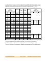
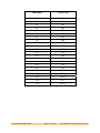
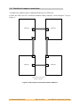
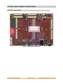
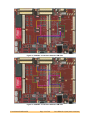
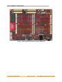
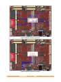
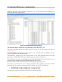
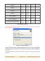
1
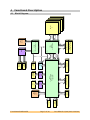
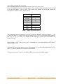
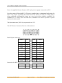
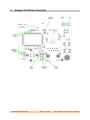
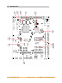
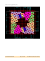
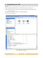
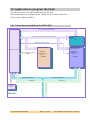
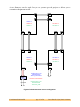
Sundance Multiprocessor Technology Limited
User Manual
Form : QCF42
Date : 6 July 2006
Unit / Module Description:
Unit / Module Number:
SMT148FX-DC, SMT148FX-ATX
Document Issue Number:
1.4
Issue Date:
3/8/09
Original Author:
GKP
User Manual
for
SMT148FX
DC and ATX versions
Sundance Multiprocessor Technology Ltd, Chiltern House,
Waterside, Chesham, Bucks. HP5 1PS.
This document is the property of Sundance and may not be copied
nor communicated to a third party without prior written
permission.
© Sundance Multiprocessor Technology Limited 2006
User Manual SMT148FX
Page 1 of 48
Last Edited: 03/08/2009 11:42:00
Revision History
Issue
Changes Made
Date
Initials
1.0
First release
4/6/07
GKP
1.1
Minor updates
2/7/07
GKP
1.2
Update LVDS FPGA connectivity.
20/8/07
GKP
Added LVDS buffer drawing.
20/8/07
GKP
Differentiated DC and ATX versions.
13/6/08
GKP
3/7/08
GKP
19/8/08
GKP
3/8/09
FS
1.2.1
1.3
1.3.1
Corrected LVDs connector pin-out tables.
Added additional detail about IL715 isolators.
1.3.2
1.4
Added connector info for RS485.
Spartan firmware explanation
Important comments or cautions are displayed next to this symbol.
User Manual SMT148FX
Page 2 of 48
Last Edited: 03/08/2009 11:42:00
Table of Contents
1
Introduction ..................................................................................................................... 5
2
Related Documents ........................................................................................................ 6
2.1
3
Referenced Documents.............................................................................................. 6
Acronyms, Abbreviations and Definitions .............................................................. 6
3.1
4
Acronyms and Abbreviations ................................................................................... 6
Functional Description.................................................................................................. 7
4.1
Block Diagram.............................................................................................................. 7
4.1.1 Virtex 4 FX ............................................................................................................... 8
4.1.2 Spartan 3.................................................................................................................. 8
4.1.3 TIM Sites................................................................................................................... 8
4.1.4 10/100/1000 Ethernet Phy................................................................................... 8
4.1.5 LVDS Isolators......................................................................................................... 9
4.1.6 Firewire................................................................................................................... 12
4.1.7 USB2........................................................................................................................ 12
4.1.8 RS232...................................................................................................................... 14
4.1.9 Flash........................................................................................................................ 14
4.1.10RS485...................................................................................................................... 15
4.1.11SHB .......................................................................................................................... 15
4.1.12LEDs ........................................................................................................................ 15
4.1.13ZBT Memory .......................................................................................................... 15
4.1.14RSL .......................................................................................................................... 16
4.1.15External ComPorts ............................................................................................... 17
4.1.16Internal ComPorts ................................................................................................ 19
4.1.17Power input (DC version).................................................................................... 20
4.1.18Power input (ATX version).................................................................................. 21
4.1.19Power output......................................................................................................... 22
4.1.20JTAG........................................................................................................................ 22
4.1.21Local Clock for ADCs etc. ................................................................................... 23
4.1.22Fan Power............................................................................................................... 23
4.1.23Reset Scheme ........................................................................................................ 23
4.1.24External FPGA Clock Input ................................................................................. 24
4.1.25FPGA (Virtex4 and Spartan) configuration ...................................................... 24
5
Jumper Position/Function.......................................................................................... 25
6
Footprint ......................................................................................................................... 26
6.1
Top View ..................................................................................................................... 26
User Manual SMT148FX
Page 3 of 48
Last Edited: 03/08/2009 11:42:00
6.2
Bottom View............................................................................................................... 27
7
Virtex4 FPGA Pin Allocation...................................................................................... 28
8
Virtex4 FPGA Bank Allocation .................................................................................. 29
9
Programming the Cpld ................................................................................................ 31
10
Application to program the Flash ............................................................................ 32
10.1 Connections provided on the SMT148FX ............................................................. 32
11
Accessing the Flash...................................................................................................... 33
11.1 Programming the Spartan ....................................................................................... 33
11.2 Erase and Program of the Flash ............................................................................. 33
11.3 Booting the Spartan and Virtex 4 from flash ...................................................... 34
12
Firmware for the Spartan. .......................................................................................... 34
12.1 Hardwired comport connections ........................................................................... 36
13
RSL and Comport connections .................................................................................. 37
13.1 RSL connections ........................................................................................................ 37
13.2 Comport connections............................................................................................... 39
14
Spartan firmware explanation................................................................................... 42
15
DIP Switches .................................................................................................................. 45
16
Support Packages ......................................................................................................... 46
17
Physical Properties....................................................................................................... 46
18
Thermal Management.................................................................................................. 47
19
Safety ............................................................................................................................... 48
20
EMC .................................................................................................................................. 48
21
Ordering Information .................................................................................................. 48
User Manual SMT148FX
Page 4 of 48
Last Edited: 03/08/2009 11:42:00
1
Introduction
The SMT148FX is a four site stand-alone TIM carrier board with several external
interfaces.
Connectors are provided to interface to:
•
RS232 – From FPGA or USB controller
•
LVDS (48 pairs)
•
JTAG
•
RSL
•
SATA – Connectors carrying RSL signals only.
•
SHB
•
RS485 (16 pairs)
•
USB2
•
Firewire (1394) interface only (No IP core).
•
Ethernet 10/100/1000
•
LED (x32)
•
ZBT memory
•
Local clock buffer/generator output
User Manual SMT148FX
Page 5 of 48
Last Edited: 03/08/2009 11:42:00
Sundance Multiprocessor Technology Limited
User Manual
Form : QCF42
Date : 6 July 2006
2 Related Documents
2.1 Referenced Documents
Sundance SLB specification (hyperlink).
Sundance RSL specification (hyperlink).
Datasheets as specified above.
Texas Instruments Module specification.
SMT118: Carrier with 3 Module sites and I/O facilities.
SMT180: Carrier with 8 Module sites.
3 Acronyms, Abbreviations and Definitions
3.1 Acronyms and Abbreviations
A list of acronyms etc (hyperlink).
User Manual SMT148FX
Page 6 of 48
Last Edited: 03/08/2009 11:42:00
User Manual SMT148FX
4 lanes
4 lanes
SATA
connectors
x4
RSL
connector
Page 7 of 48
JTAG
header
LEDs
x32
Firewire
connector
IEEE1394
PHY
FPGA
Virtex4 XC4VFX60
FF1152 package
1.2V core
LVDS connectors x4
Ethernet
PHY
RJ45
8x 6-bit
16-bit
RS485
connector
ZBT
memory
2x 2Mx18
Global Bus
3x
ComPorts
Flash
memory
2x 16-bit
SHB
FPGA
Spartan 3
ComPort switch
Select map port
External ComPorts x4
via SHB connectors
External ComPort
via 26-way 3m header
JTAG
CPLD
FPGA configuration control
JTAG
USB2
5x
ComPorts
SHB
connector
JTAG
Select map port
USB
connector
RS232
connector
16x
ComPorts
TIM sites
x4
TIM sites
x4
TIM sites
x4
TIM sites
x4
4 Functional Description
4.1 Block Diagram
Last Edited: 03/08/2009 11:42:00
4.1.1 Virtex 4 FX
The primary controlling device on the 148FX is the Xilinx Virtex4 FX60 FPGA. This
device is an FF1152 package which provides 16 MGTs (high speed serial I/O) and
576 normal I/O signals.
This device can be configured via a Xilinx compatible JTAG header.
In normal operation, this device is configured by the CPLD (XC2C512). The
configuration data is stored in flash memory, and is loaded using slave SelectMAP
mode (8-bit parallel).
4.1.2 Spartan 3
The Xilinx Spartan 3 device is similar in nature to that employed on the SMT150Q
and SMT329 carrier boards. It acts as a pre-configured ComPort routing switch.
Different ComPort routing schemes are easy to implement using supplied tools
(requires Xilinx ISE development software).
This device is also configured by the CPLD, and uses slave SelectMAP mode (8-bit
parallel), but is also part of the Xilinx JTAG chain.
4.1.3 TIM Sites
The 148FX provides 4 TIM sites. In addition to the standard specification
requirements, the 148FX also provides the 3.3V supply to the two TIM mounting
holes.
Each TIM site has 4 ComPorts connected directly to the Spartan 3 device. The two
remaining ComPorts are used to create a simple pipe, with each site connecting to
its nearest neighbours.
The TIM site’s interrupt, timer, config, and reset pins are all connected to the Virtex
4 FPGA. The reset signals are asserted during power-up, when pressing the on-board
reset button, or when signalled to via one of the external ComPort connectors.
A global bus connection (16 bit data, 12 bit address) is also made from each site to
the Virtex 4. The global bus connector normally contains one 16-bit SDB interface
(this is unlike the TIM specification which describes the global bus as an
Address/Data structure). These SDBs are the primary method of communication to
the resources shared by the Virtex 4 (eg. USB, Firewire, etc).
4.1.4 10/100/1000 Ethernet Phy
A Marvell Ethernet PHY connects directly to the Virtex 4 FPGA. This interfaces to a
10/100/1000 network via a standard RJ45 socket. This socket has built-in
magnetics.
The PHY is controlled by a MAC within the Virtex 4.
An Ethernet IP core is not supplied in the standard firmware. Please
contact Sundance for further information.
User Manual SMT148FX
Page 8 of 48
Last Edited: 03/08/2009 11:42:00
4.1.5 LVDS Isolators
48 single ended signals are connected from the Virtex 4 to LVDS drivers and
receivers (SN65LVDS390/1) via galvanic isolators (type IL715-3). The transmitter
part is enabled via control signals. The LVDS outputs are arranged in groups of 6.,
hence there are 8 control signals. The LVDS receivers are enabled continuously.
The isolation provided is up to 150V rms maximum.
The isolation provided is up to 150V rms, whilst still enabling a baud rate of up to
100Mbps.
The LVDS transmitters and receivers are external to the FPGA itself. The devices
used are SN65LVDS390 and 391.
LVTTL input from
FPGA
Output Enable
(goes to 3 drivers)
LVTTL input from
FPGA
TX+
Differential output
to D-connector
LVDS driver
TX-
LVTTL output to
FPGA
RX+
Differential input
from D-connector
LVDS receiver
RX100 Ohm
termination
resistor
The IL715-3 galvanic isolators require a simple initialisation sequence
before use. Simply toggle the driving pins from the FPGA to the IL715-3
devices at start-up.
User Manual SMT148FX
Page 9 of 48
Last Edited: 03/08/2009 11:42:00
Typically. The TIMs are configured to route their McBSPs to the global bus connector
pins, which, in turn, are routed to the LVDS I/O. The following table shows the pinout for the 37-way D-type connectors. This is only applicable if the TIM is using nonstandard firmware which routes McBSP signals onto the global bus. Contact
Sundance for further information.
GND
Input/Output
20
GND
McBSP_CLKR_Tx_0+
I
21
McBSP_CLKR_Tx_0-
3
McBSP_FSR_Tx_0+
I
22
McBSP_FSR_Tx_0-
4
McBSP_DR_Tx_0+
I
23
McBSP_DR_Tx_0-
5
GND
1
2
24
GND
McBSP_CLKX_Tx_0+
O
25
McBSP_CLKX_Tx_0-
7
McBSP_FSX_Tx_0+
O
26
McBSP_FSX_Tx_0-
8
McBSP_DX_Tx_0+
O
27
McBSP_DX_Tx_0-
9
GND
28
GND
10
GND
11
GND
6
29
GND
McBSP_CLKR_Tx_1-
I
30
McBSP_CLKR_Tx_1+
13
McBSP_FSR_Tx_1-
I
31
McBSP_FSR_Tx_1+
14
McBSP_DR_Tx_1-
I
32
McBSP_DR_Tx_1+
15
GND
12
33
GND
McBSP_CLKX_Tx_1-
O
34
McBSP_CLKX_Tx_1+
17
McBSP_FSX_Tx_1-
O
35
McBSP_FSX_Tx_1+
18
McBSP_DX_Tx_1-
O
36
McBSP_DX_Tx_1+
19
GND
37
GND
16
User Manual SMT148FX
Page 10 of 48
Last Edited: 03/08/2009 11:42:00
As the LVDS drivers are connected directly to the FX60 FPGA, they can be driven
from this device without need for the above McBSP method. The following table
shows the connectivity between the FPGA and the D-connectors (P2, 3, 4 & 5):
DConn
Pin
DConn
Pin
Signal
GND
1
20
GND
Signal
FPGA
signal pin
P2
P3
P4
P5
FPGA
enable pin
D29
K29
M26 P31
RX0+
2
21
RX0-
F31
C32
L30
P26
RX1+
3
22
RX1-
E32
D32 L31
P27
RX2+
4
23
RX2-
GND
5
24
GND
D31
E29
K31
M31
TX0+
6
25
TX0-
E31
F29
K32
M32
TX1+
7
26
TX1-
C29
J29
M25 P30
TX2+
8
27
TX2-
GND
9
28
GND
GND
10
GND
11
29
GND
C30
L28
M28 P29
RX3-
12
30
RX3+
D30
L29
N27
R29
RX4-
13
31
RX4+
G31
H29 M30 R27
RX5-
14
32
RX5+
GND
15
33
GND
H28 J31
J32
P32
TX3-
16
34
TX3+
F30
J27
N28
R31
TX4-
17
35
TX4+
G30
K28
N29
R32
TX5-
18
36
TX5+
GND
19
37
GND
P2
P3
P4
H27
J30
G32
H30 N30
P5
H32 N32
R28
The LVDS transmitters are enabled in groups. Two groups per D-connector.
Eg. FPGA pin J30 is the transmitter enable for connector P3’s TX pins.
The LVDS receivers are continuously enabled and terminated by a 100 Ohm resistor.
User Manual SMT148FX
Page 11 of 48
Last Edited: 03/08/2009 11:42:00
4.1.6 Firewire
A single IEEE1394 interface is provided by an Agere FW801A PHY. The following
table shows the pinout of the connector;
1
Cable Power
2
GND
3
TPB-
4
TPB+
5
TPA-
6
TPA+
This will allow high speed firewire data to be routed directly to the FPGA.
The standard FPGA firmware does not include an IEEE1394 IP core. These
are available from 3rd parties. Please contact Sundance for further
information.
4.1.7 USB2
The USB2 interface is provided by the Cypress CY7C68013A device.
The Cypress part, in addition to providing USB functions with a FIFO type interface,
also contains a USART, and an 8051 micro-controller.
The USB connector pin-out is shown here;
1
USB_ind
2
Data-
3
Data+
4
GND
The interface provided by this controller looks identical to a 16-bit SDB interface,
and is routed directly to the Spartan FPGA and the CPLD.
The standard Cypress firmware does not include functions to control the
USART. Please contact Sundance for further information.
The following table shows the Cypress pin connectivity to the Sundance SDB signal;
User Manual SMT148FX
Page 12 of 48
Last Edited: 03/08/2009 11:42:00
User Manual SMT148FX
SDB Signal
Cypress Pin
CLK
IFCLK
D0
PB0
D1
PB1
D2
PB2
D3
PB3
D4
PB4
D5
PB5
D6
PB6
D7
PB7
D8
PD0
D9
PD1
D10
PD2
D11
PD3
D12
PD4
D13
PD5
D14
PD6
D15
PD7
WEN
RDY0
REQ
CTL2
ACK
RDY1
UD0
PA7
UD1
RDY3
Page 13 of 48
Last Edited: 03/08/2009 11:42:00
4.1.8 RS232
Two devices generate RS232 data (simple TX and RX); the FPGA and the USB2
controller.
The Rx data pin from a 9-way D-type connector is connected to both serial
interfaces. The Tx data pin from each device is routed to a jumper block (JP12)
which allows the selection of one Tx data output. The RS232 levels are generated
using a MAX3227 converter.
1
2
Rx
3
Tx
4
5
GND
6
7
8
9
Insert only one jumper in positions shown in section 7.
4.1.9 Flash
The flash memory connected to the CPLD and contains configuration data for the
two FPGAs.
Any additional space within this device can be used to store application programs.
The flash can be directly programmed by the CPLD only.
The external ComPort is directly connected to the CPLD. This allows the
reprogramming of the flash using an identical procedure as that employed on the
SMT348. After configuration, the CPLD ComPort is tri-stated and the external
ComPort functions as an input to the ComPort switch (Spartan 3).
User Manual SMT148FX
Page 14 of 48
Last Edited: 03/08/2009 11:42:00
4.1.10 RS485
Each of the 16 RS485 signal pairs is driven by an SN75HVD12. They are arranged
into two groups of 8-bits each and have a single control signal which selects the
group to be a transmitter or receiver.
Connector RS1 carries these signals.
Function
S0S1S2S3S4S5S6S7GND
GND
pin
1
3
5
7
9
11
13
15
17
19
pin
2
4
6
8
10
12
14
16
18
20
Function
S0+
S1+
S2+
S3+
S4+
S5+
S6+
S7+
GND
GND
Function
GND
GND
S8S9S10S11S12S13S14S15-
pin
21
23
25
27
29
31
33
35
37
39
pin
22
24
26
28
30
32
34
36
38
40
Function
GND
GND
S8+
S9+
S10+
S11+
S12+
S13+
S14+
S15+
4.1.11 SHB
A single SHB connector (Samtec QSH-030-01) provides two independent 16-bit
SDBs, or a single 32-bit SDB interface. These signals are connected directly to the
FX60.
4.1.12 LEDs
32 LEDs are connected to the Virtex 4 FPGA in a matrix of 8x4.
4.1.13 ZBT Memory
Two 16-bit wide ZBT memories are connected directly to the FPGA. This provides a
memory bank of 2Mx16 bits (4Mbytes).
The standard FPGA firmware does not include functions to control the
ZBTRAM. VHDL test code is available. Please contact Sundance for
further information.
User Manual SMT148FX
Page 15 of 48
Last Edited: 03/08/2009 11:42:00
4.1.14 RSL
The Virtex 4 FX FPGA provides 16 RSL (Rocket Serial Link) interfaces. 8 of these are
connected to the 4 TIM sites (2 per site).
Four RSLs are connected to 4 SATA style connectors thus allowing inter-board
connectivity.
The remaining 4 are presented on a standard RSL connector. See the RSL
specification for details on the connector type.
The SATA style connectors do NOT provide a SATA interface using the
standard Sundance FPGA firmware.
RSL interfaces provide a high-speed (250Mbytes/s per link) bi-directional
connection. Fast communication between TIMs should use these links wherever
possible.
User Manual SMT148FX
Page 16 of 48
Last Edited: 03/08/2009 11:42:00
4.1.15 External ComPorts
Four ComPorts are connected to SHB style connectors. Two output-type ComPorts (0
and 1), and two input-type ComPorts (3 and 4) are provided. All 4 ComPorts are
connected to both SHB-style connectors. Connector A is arranged 0, 1, 3 and 4, and
connector B 3, 4, 0 and 1. With this scheme, a simple one-to-one SHB cable can be
used to connect connector A on one 148FX to connector B on another 148FX.
External Comports 0, 1, 3 and 4 are routed to two SHB connectors (Samtec QSH-03001) to allow connection to another SMT148FX carrier and its ComPorts. The pin-out
is as follow:
1
STRB_0
2
RDY_0
3
REQ_0
4
ACK_0
5
D0_0
6
D1_0
7
D2_0
8
D3_0
9
D4_0
10
D5_0
11
D6_0
12
D7_0
15
STRB_1
16
RDY_1
13
14
17
REQ_1
18
ACK_1
19
D0_1
20
D1_1
21
D2_1
22
D3_1
23
D4_1
24
D5_1
25
D6_1
26
D7_1
27
29
STRB_3
30
RDY_3
31
REQ_3
32
ACK_3
33
D0_3
34
D1_3
35
D2_3
36
D3_3
37
D4_3
38
D5_3
39
D6_3
40
D7_3
43
STRB_4
44
RDY_4
41
42
28
45
REQ_4
46
ACK_4
47
D0_4
48
D1_4
49
D2_4
50
D3_4
51
D4_4
52
D5_4
53
D6_4
54
D7_4
55
56
59
60
57
58
RESET
Compatible with the 148 and 148LT, an active low RESET signal is provided. When
two 148FX boards are interconnected with a 60 way cable assembly, the RESET is
propagated from one 148FX to the other.
User Manual SMT148FX
Page 17 of 48
Last Edited: 03/08/2009 11:42:00
Another ComPort is available via a 26-way connector, where cable SMT502 can be
used to connect to a SMT310Q and download applications from a PC. This connector
has the following pin-out.
User Manual SMT148FX
1
CSTRB
2
GND
3
CRDY
4
GND
5
CREQ
6
GND
7
CACK
8
GND
9
D0
10
D1
11
D2
12
D3
13
D4
14
D5
15
D6
16
D7
17
3.3V
18
GND
19
/RESETOUT
20
GND
21
/RESETIN
22
GND
23
NC
24
NC
Page 18 of 48
Last Edited: 03/08/2009 11:42:00
4.1.16 Internal ComPorts
Each TIM site has 6 ComPorts.
Four of these are connected directly to the Spartan 3 FPGA. These are ComPorts 0, 1,
3 & 4.
ComPorts 2 & 5 are connected between TIM sites in a pipe configuration as follows;
TIM1 ComPort 2 connects to TIM2 ComPort 5
TIM2 ComPort 2 connects to TIM3 ComPort 5
TIM3 ComPort 2 connects to TIM4 ComPort 5
TIM4 ComPort 2 connects to TIM1 ComPort 5
User Manual SMT148FX
Page 19 of 48
Last Edited: 03/08/2009 11:42:00
4.1.17 Power input (DC version)
Power is supplied from an external source. The voltage of the external source needs
to be in the range +18V to 30V. This enters the board via an 8-pin connector
(Receptacle, mini fit 8 Way, Molex) JP14.
+18-30V
1
+18-30V
2
+18-30V
3
+18-30V
4
GND
5
GND
6
GND
7
GND
8
Table 1 : Power in connector pinout
The external source is input to a DC-DC converter module, which produces +/-12V
to the TIM sites. It is also used as an input to two DC-DC converters that produce
the +5V, +3.3V, +2.5V and 1.5V supply to the TIM sites, carrier FPGA and other onboard devices.
When using a +24V input, the power consumption of an unpopulated SMT148X is
approximately 6W.
Alternatively, the input power can be provided at +9 to 18V (using alternative DCDC
parts). Contact Sundance for further information.
The fan connectors, FAN1-4, are powered directly from the input supply.
User Manual SMT148FX
Page 20 of 48
Last Edited: 03/08/2009 11:42:00
4.1.18 Power input (ATX version)
Power is supplied directly from an ATX style power supply connected to JP15.
Note that most off-the-shelf PC ATX power supplies have a minimum load rating for
their +12V output. Typically, this can be about 1A. Fitting a couple of cooling fans is
often sufficient. Alternatively, there are zero load power supplies available. Eg.
Lambda NV-175 series (NV1-453TTH-N3-I). Sundance are able to provide a power
harness for this model.
The fan connectors, FAN1-4, are powered at +12V.
The ATX Power Connector Pin-Out is shown here:
Main 20 pin connector:
Name
Pin
Pin
Name
+3.3V
1
11
+3.3V
+3.3V
2
12
-12V
GND
3
13
GND
+5V
4
14
ON (input)
GND
5
15
GND
+5V
6
16
GND
GND
7
17
GND
-
8
18
-
-
9
19
+5V
+12V
10
20
+5V
Extension for BTX:
User Manual SMT148FX
+12V
+5V
+3.3V
GND
Page 21 of 48
Last Edited: 03/08/2009 11:42:00
4.1.19 Power output
Power can be supplied to external devices or modules. The 8-pin connector
(Receptacle, mini fit 8 Way, Molex) JP16 provides several voltages and has the
following pinout:
Pin number
-12V
1
+12V
2
+5V
3
+3.3V
4
GND
5
GND
6
GND
7
Key
8
Table 2 : Power out pinout
Connector position 8 is filled to prevent plugging in the power input
cable (the connectors are the same type). A modified plug (pin 8
removed) must be used for power output.
4.1.20 JTAG
A single JTAG chain connects all 4 TIM sites and the JTAG in & out connectors. This
chain is used with the TI Code Composer Studio software suite. Although in essence
it is a chain, the chain exists internally to a Xilinx CPLD. The CPLD drives and
receives signals to the 4 TIM sites independently. This allows JTAG clock
frequencies in excess of 30MHz to work reliably.
The JTAG-out (JTAG2) connector can be connected to the JTAG-in (JTAG1) connector
of other SMT148FX, thus extending the chain (see cable SMT503).
All JTAG chaining and TIM bypass is performed within the CPLD.
User Manual SMT148FX
Page 22 of 48
Last Edited: 03/08/2009 11:42:00
4.1.21 Local Clock for ADCs etc.
The full functionality of the SMT399-F is also included. This comprises an external
clock input, phase shifter, local OCXO, and 4-way power splitter.
Selection between local OCXO and VGA is made with the position of a 0 Ohm
resistor link. This link (labelled R125) is located on the reverse of the board near the
RS232’s 9-way d-connector. Moving this link will not invalidate any warranty.
Some soldering is necessary to select between the two options.
J1-4 are outputs from a power splitter which is fed from the OCXO. These outputs
are intended for the Sundance range of ADC/DAC modules.
Connector J5 is used for an external clock input which enters the VGA (variable gain
amplifier).
4.1.22 Fan Power
Four two-pin connectors are provided to supply fans using power directly from the
power input connector.
Note that if power is provided via an ATX type supply, then these fan
connectors will be powered at +12V.
4.1.23 Reset Scheme
A power rail monitor observes the state of the 3.3V supply. This device will generate
a reset to the SMT148FX (RESET148) during power-up or if the 3.3V supply drops
below 3V. This signal is an open-collector output and is also driven to the inter-card
ComPort connector, and thus to another SMT148FX.
The POR (power on reset) signal is driven to the RESETOUT pin on the external
ComPort1 connector. The RESETIN pin on the above connector is buffered by an
open-collector device which in turn can also drive the RESET148 signal. An
additional 4 pin header is provided to allow other devices to share the opencollector RESET148 signal.
The TIM reset pins are connected to the FPGA and will be reset when RESET148 is
active as well as when some firmware conditions trigger a reset to the different TIMs
(see Firmware description for more details about TIM reset).
User Manual SMT148FX
Page 23 of 48
Last Edited: 03/08/2009 11:42:00
4.1.24 External FPGA Clock Input
Located near the DSP JTAG headers, connector J6 provides a direct connection to
the FPGA pin H17. This has 50 Ohm termination and is suitable for LVTTL
(maximum 3.3V) signals only.
4.1.25 FPGA (Virtex4 and Spartan) configuration
The Virtex4 FPGA can be configured from flash, USB or ComPort. This is determined
by the setting of switch bank SW3, and is detailed in the following table. Note that
SW4-1 must be set to OFF.
The Jumpers [1-2] of SW3 control the Spartan configuration
The Jumpers [3-4] of SW3 control the Virtex4 configuration.
SW3
Position 2 or 4 Position 1 or 3
Flash
ON
ON
Comport
OFF
ON
USB
ON
OFF
Examples:
Virtex 4
Spartan
4
3
2
1
Both devices configure from Flash.
ON
ON
ON
ON
Direct configuration via USB.
ON
OFF ON OFF
SW3
(needs a host application to send the bitstreams via USB)
Configuration of Spartan via Flash and of Virtex 4 via CP3 OFF
connected to TIM site 1 CP0.
ON
ON
ON
The Spartan is always the device configured first.
It is possible to download a new configuration to the FPGA using a Xilinx JTAG cable
connected to a PC and to JP6 on the SMT148FX carrier. This uses the standard 14way ribbon cable supplied by Xilinx. Refer to Xilinx document DS300 v3.1 page 8 for
details of the pinout.
User Manual SMT148FX
Page 24 of 48
Last Edited: 03/08/2009 11:42:00
5 Jumper Position/Function
User Manual SMT148FX
Page 25 of 48
Last Edited: 03/08/2009 11:42:00
6 Footprint
6.1 Top View
User Manual SMT148FX
Page 26 of 48
Last Edited: 03/08/2009 11:42:00
6.2 Bottom View
User Manual SMT148FX
Page 27 of 48
Last Edited: 03/08/2009 11:42:00
7 Virtex4 FPGA Pin Allocation
USB2 controller
Firewire / OXUF922
CLK
1
Data
16
Control
3
User Def
2
All
Address
SHB/SDB
12
Data
8
Control
3
Data
16
22
SDB type interface
29
IDE interface to OXUF922
23
From OXUF922
V4 Configuration data
2
48
2 x 16-bit data.
Control
3
WEN, REQ, ACK.
User
4
USER0-3
Clock
1
RS485
All
18
16 data and two control.
LVDS
All
56
8 groups of 7, normally routed to McBSPs via FPGA.
ComPorts
All
48
To Spartan3.
LEDs
All
12
8 x 4 matrix.
Ethernet PHY
All
12
4-bit data + 2 control for each direction.
12
4
4
Global Bus
TIM misc
Address
12
Data
16
4
TCLK
2
Config
1
IIOF,NMI
4
IACK
1
Reset
1
Individual resets to TIM sites.
Clock
3
CLKIN, H1 and H3.
All
ZBT
Address
20
Data
32
Control+Clk
10
Other
User Manual SMT148FX
128
Control
RS232
Spartan3
4
RST, COMA, MDC and MDIO.
STRB, RW, PAGE, RDY
4
48
2
1
Tx + Rx.
62
FPGA config
3
PROG, CCLK, DIN
Data Interface
4
CLK25, PXCLK, PXDATA, PXLOAD
Reset
1
From V4
2
BDRESET, CLK50
Page 28 of 48
Last Edited: 03/08/2009 11:42:00
8 Virtex4 FPGA Bank Allocation
Interface
Bank
Comment
Global Bus A
5
12 Address, 16 Data, 4 Control (STRB, RDY, WR, PAGE)
Global Bus B
6+10
12 Address, 16 Data, 4 Control (STRB, RDY, WR, PAGE)
Global Bus C
8
12 Address, 16 Data, 4 Control (STRB, RDY, WR, PAGE)
Global Bus D
11
12 Address, 16 Data, 4 Control (STRB, RDY, WR, PAGE)
ZBT Bank 1
10
Clock uses GCK on bank
ZBT Bank 2
12
Clock uses GCK on bank
Ethernet
12
SHB
7
RS485
7+8
Direction control is on bank 8.
ComPorts
11+5
2 ports per bank used.
LVDS
9
USB
8
LEDs
5+9
Misc, TIM
1+3+4
RS232
5
RST, Clock
5
IEEE1394
6
TIM reset
11
V4 to S3 interface
User Manual SMT148FX
Appears as a 16 bit SDB.
8
Tx, Rx.
CLK, DATA, LOAD, RESET
Page 29 of 48
Last Edited: 03/08/2009 11:42:00
This is shown graphically here,
User Manual SMT148FX
Page 30 of 48
Last Edited: 03/08/2009 11:42:00
9 Programming the Cpld
The cpld firmware is necessary to access the flash and to configure the SMT148-FX
FPGAs..
Please use Xilinx download cable to download the cpld jedec file top.jed.
Select the CPLD XC2C512 from the 3 components and download the file top.jed.
•
It can be found in:
$\Program Files\Sundance\SMT6048\ FlashProgramming
This is a one off operation.
Figure 1:SMT148FX JTAG chain
User Manual SMT148FX
Page 31 of 48
Last Edited: 03/08/2009 11:42:00
10 Application to program the Flash
The Host can access the SMT148FX flash via the USB.
Before the Spartan is configured, the CPLD provides a link to the USB.
It also is the Flash controller.
10.1 Connections provided on the SMT148FX
Flash control signals and address bus
Flash control
Common signals and buses for configuration purposes
Configuration
data
Flash
Independent configuration signals
Common Configuration
signals and data bus
D[7:0], CCLK, RDWR_B
Coolrunner II CPLD
Independent configuration/control
signals
Independent
configuration/control
signals
Independent
configuration/control
signals
Spartan 3
Switch control signals
Virtex4Fx
BUFFERED COMPORT 3
Configuration
Switch
SMT148FX
User Manual SMT148FX
USB DEVICE
B
U
F
F
E
R
E
D
C
O
M
P
O
R
T
3
BUFFERED COMPORT 3
USB DEVICE
U
S
B
D
E
V
I
C
E
Page 32 of 48
Last Edited: 03/08/2009 11:42:00
11 Accessing the Flash
This section describes the various steps to follow to access the Flash.
11.1 Programming the Spartan
Set the switches of the SMT148FX with SW3 [4-3-2-1]= ON ON ON ON and
SW4[4-3-2-1] = OFF OFF OFF ON.
SW4 [1] ON provides Programming and erase accesses of the Flash.
SW4 [1] OFF disables these accesses and enables read accesses only of the Flash in a
view to program the FPGAs.
Reset or power off and on the SMT148FX evytime you change the switch settings..
11.2 Erase and Program of the Flash
Sundance provides 2 download utilities:
•
•
The SMT6002 is a free utility downloadable with the Sundance wizard.
o
The Spartan firmware MUST be located at address 0x0.
o
The Virtex 4 firmware MUST be located at address 0x800000.
The SMT6048 package provides a host utility called FlashUtility.exe.
o
Tick the option for the relevant FPGA and you can delete/ program a
new firmware for it.
Browse to the firmware of your choice for the SMT148FX Spartan or the Virtex
4(after the next power up, it will be loaded from Flash in the Spartan and/or the
Virtex4.)
It can be found in:
$\Program Files\Sundance\SMT6002\Firmware\Smt148FX
You always need to delete the current bitstream before replacing
it with a new bitstream in Flash.
Deleting a bitstream is quick, but erasing the whole flash can take 2 minutes.
Programming takes about 1 minute.
User Manual SMT148FX
Page 33 of 48
Last Edited: 03/08/2009 11:42:00
11.3 Booting the Spartan and Virtex 4 from flash
Then set the switch SW4[4-3-2-1] = OFF OFF OFF OFF.
The Spartan and Virtex 4 will configure from Flash next time you issue a hard reset
or power on the SMT148FX.
Any Spartan design available flashes led 2 while the Virtex4 example design
provided flashes the whole raw of leds next to led2.
12 Firmware for the Spartan.
It can be found in: $\Program Files\Sundance\SMT6002\Firmware\Smt148FX
The default firmware “com.sundance.smt148-fx.sc3s1500.usb_default.app” present
in flash, enables default comport connections between TIM sites and a direct
connection between USB and TIM site 1 comport 3. The connections are represented
by Figure 2: Default bitstream comport configuration.
More firmware are available to allow different TIM connections.
The default_anticlockwise firmware
“com.sundance.smt148-fx.sc3s1500.usb_default_anticlockwise.app” provides the
same comport connections as before, but this time going from TIM1 to TIM4 to
TIM3 to TIM2 to TIM1.
The default_dual_TIM firmware
“com.sundance.smt148-fx.sc3s1500.usb_default.dual_TIM.app” provides the same
comport connections as before, but this time going from TIM4 to TIM1 to TIM2 to
TIM3 to TIM4.
For more advanced use, the SMT148-FX Virtex4 FPGA is available for customisation
A custom firmware for the Spartan to show that the Virex 4 can be part of the
network of processors in a Diamond application is provided with
“com.sundance.smt148-fx.sc3s1500.Tim2Cpld.app”.
The comport link used between TIM1 and the virtex4 is TIM1 CP0 to Virtex4 CP3.
(this link is only for configuration and not yet available as a valid link after
configuration…will be in the next release).
Another link is declared and can be used for communicaton once the application is
loaded. The connections made are TIM1 CP4 to Virtex4 CP1.
Feel free to make a Diamond application including a TIM on TIM site 1 and a design
on the Virtex 4.
Use the Diamond server to load the .app and you should see the virtex 4
configuring. (do not forget to check the SMT148-FX switches)
User Manual SMT148FX
Page 34 of 48
Last Edited: 03/08/2009 11:42:00
A new firmware can be made for you or you can get the project to allow you to
customise the Spartan at will…
0
3
1
4
TIM SITE 4
TIM SITE 3
TIM SITE 2
TIM SITE 3
TIM SITE 1
TIM SITE 2
3
4
1
0
0
1
4
3
TIM SITE 1
TIM SITE 2
TIM SITE 1
TIM SITE 4
TIM SITE 4
TIM SITE 3
4
3
1
0
Implementation in the
bitsream entitled
“default_anticlockwise”
Fx2lp
Implementation in the
bitsream entitled “default”
Usb cable
Implementation in the
bitsream entitled
“default.dual_TIM”
Figure 2: Default bitstream comport configuration.
User Manual SMT148FX
Page 35 of 48
Last Edited: 03/08/2009 11:42:00
12.1 Hardwired comport connections
A hardwired comport pipe is implemented between TIM sites.
It links the TIM sites in a clockwise manner using comport 2 and comport 5 as per
Figure 3.
TIM SITE 2
TIM SITE 1
2
5
5
2
2
5
5
2
TIM SITE 3
TIM SITE 4
PCB Comport connections
between TIM sites
Figure 3: PCB comport connections between TIM sites
User Manual SMT148FX
Page 36 of 48
Last Edited: 03/08/2009 11:42:00
13 RSL and Comport connections
13.1 RSL connections
Figure 4: Virtex 4 RSL connections
User Manual SMT148FX
Page 37 of 48
Last Edited: 03/08/2009 11:42:00
Figure 5: PCB RSL connections between TIM sites
Figure 6: PCB RSL connections between TIM sites
User Manual SMT148FX
Page 38 of 48
Last Edited: 03/08/2009 11:42:00
13.2 Comport connections
Figure 7: PCB comport connections between TIM sites
User Manual SMT148FX
Page 39 of 48
Last Edited: 03/08/2009 11:42:00
Figure 8: Spartan comport connections
Figure 9: Spartan comport connections
User Manual SMT148FX
Page 40 of 48
Last Edited: 03/08/2009 11:42:00
Figure 10: Spartan to Virtex 4, CPLD and USB comport connections
The comport used to configure the Virtex 4 can’t be re-used after the FPGA
configuration. It’s why the comport 5 is used in a Diamond project, this comport is
not connected on the PCB. If you select one of the three comport available on the
Virtex 4 as its configuration comport, you will not be able to use this comport for
data transfer after the FPGA configuration.
User Manual SMT148FX
Page 41 of 48
Last Edited: 03/08/2009 11:42:00
14 Spartan firmware explanation
Sundance provides many Spartan firmwares; you can design your own firmware in
following the next instructions.
Figure 11: Default Spartan firmware project
The firmware must contain the clock manager task: SMT148FX_CM
The clock domain named here ifclk must be used for all the tasks and all the
connections.
The SMT148FX_CM task is used to generate this clock domain at 48MHz; it’s the
only one that uses the default clock.
The heartbeat_wrapper_ngc task corresponds to the LED Spartan status; this task
just has to be added to the project and doesn’t need any connection.
The fx2lprxtx_ngc task corresponds to the USB connection, connect this task to your
root processor location, for the default firmware, it’s T1CP3.
Between all the connections you must add a pipe_wrapper_ngc task.
You have to connect the two comport direction, for example with the default
firmware, for the connection between the USB and the T1CP3 we will have:
•
fx2lprxtx_ngcÙ pipe_wrapper_ngc_1Ùroot CP:2(TX)
•
root CP:2(TX) Ù pipe_wrapper_ngc Ù fx2lprxtx_ngc
The Spartan comport connection is list in the following table.
User Manual SMT148FX
Page 42 of 48
Last Edited: 03/08/2009 11:42:00
TIM Site 1
TIM Site 2
TIM Site 3
TIM Site 4
Virtex 4 comports
root CP:0
root CP:1
root CP:2
root CP:16
T1CP0
T1CP1
T1CP3
T1CP4
root CP:4
root CP:5
root CP:6
root CP:7
T2CP0
T2CP1
T2CP3
T2CP4
root CP:8
root CP:9
root CP:10
root CP:11
T3CP0
T3CP1
T3CP3
T3CP4
root CP:12
root CP:13
root CP:14
root CP:15
T4CP0
T4CP1
T4CP3
T4CP4
root CP:21
root CP:22
root CP:23
V4CP0
V4CP1
V4CP3
root CP:17
root CP:18
root CP:19
root CP:20
JPCP0
JPCP1
JPCP3
JPCP4
root CP:3
Virtex 4 configuration
CBUF
Connection to another SMT148FX
Table 3: Spartan connections
Don’t forget to edit all the connection and select the ifclk clock domain and select
the right link starts up properties.
Figure 12: Connection properties
At reset you must connect a comport from RX to TX or TX to RX. For the default
firmware, the T1CP3 of the TIM root processor is RX at reset, to get its bitstream.
The Spartan firmware comport (root CP:2) will have the link starts up as transmitter
properties.
The next Diagram shows the Default firmware connection with all the connections
properties.
User Manual SMT148FX
Page 43 of 48
Last Edited: 03/08/2009 11:42:00
Figure 13: Default Spartan firmware diagram
User Manual SMT148FX
Page 44 of 48
Last Edited: 03/08/2009 11:42:00
15 DIP Switches
SW4
1
Programming/Erase of the Flash
ON
Flash Reads in a view to configure FPGAs
OFF
Table 4: Switch SW4
The Spartan and Virtex 4 configuration sources can be identified using SW3.
The Jumpers [1-2] of SW3 are controlling the Spartan configuration
The Jumpers [3-4] of SW3 are controlling the Virtex4 configuration.
SW3
Flash
Jumper 2 or jumper 4 Jumper 1 or Jumper3
ON
ON
Comport OFF
ON
USB
OFF
ON
Table 5: Switch SW3.
The Comport as a source is a feature only supported for Virtex 4 configuration.
Examples:
When SW4[1] is OFF:
Virtex 4
Spartan
SW3
4
3
2
1
Both devices configure from Flash.
ON
ON
ON ON
Direct configuration via USB.
ON
OFF ON OFF
(needs a host application to send the bitstreams via USB)
Configuration of Spartan via Flash and of Virtex 4 via CP3 OFF ON
connected to TIM site 1 CP0.
ON ON
Table 6: Examples of Switch configuration.
The Spartan is always the device configured first.
Do not try to configure the Virtex 4 before configuring the Spartan or the
configuration will fail.
When SW4[1] is ON, SW3[4321] should be set to ON ON ON ON.
User Manual SMT148FX
Page 45 of 48
Last Edited: 03/08/2009 11:42:00
16 Support Packages
To be added.
17 Physical Properties
Dimensions
250 x 200mm
Weight
350g
The following table indicates the power capabilities of the on-board supplies;
Option
Supply Current
A
B
C
+12V
1.67A
0.83A
*
+5V
10A
10A
*
+3.3V
10A
10A
*
-5V
0A
0A
*
-12V
0A
0.83A
*
*Option C is with the use of an external ATX power supply. Refer to the relevant
power supply specification in this case.
MTBF
User Manual SMT148FX
Page 46 of 48
Last Edited: 03/08/2009 11:42:00
18 Thermal Management
Although provision is made to attach DC fans to the SMT148FX (powered directly
from the input voltage), correct enclosure air flow should be ensured.
Sundance are able to provide a heat-pipe type thermal management solution for two
TIM sites (sites 2 and 3). This involves increased height TIM and RSL connectors for
these sites, the fixing of the heat-pipe system direct to the TIMs’ components, and
the addition of an off-board heatsink and fan. Please consult Sundance for pricing
and availability for this option.
Several components in both the onboard 3.3V and 5.0V supplies are rated at 125°C
maximum. Without adequate cooling, the inductors in this circuit can reach in
excess of 170°C when running at full rated load.
Some of the major components are located on the underside of the
carrier board. This will allow heatsinks (or indeed an enclosure) to be
fitted.
User Manual SMT148FX
Page 47 of 48
Last Edited: 03/08/2009 11:42:00
19 Safety
This module presents no hazard to the user when in normal use.
20 EMC
This module is designed to operate from within an enclosed host system, which is
built to provide EMC shielding. Operation within the EU EMC guidelines is not
guaranteed unless it is installed within an adequate host system.
This unit is protected from damage by fast voltage transients originating from
outside the host system which may be introduced through the output cables.
Short circuiting any output to ground (except the bi-directional reset output) does
not cause the system to lock up or reboot.
21 Ordering Information
Several variations of this product are available.
SMT148-FX-DC
Standard product with on-board voltage converters.
SMT148-FX-ATX
Standard product with ATX PSU input connector.
SMT148-FX-nn-Fxxx
With additional local ADC oscillator. xxx refers to the
oscillator frequency. nn refers to power input type.
User Manual SMT148FX
Page 48 of 48
Last Edited: 03/08/2009 11:42:00


![[APPLICATION FUNCT.] (FUn-) menu](http://vs1.manualzilla.com/store/data/005824711_1-335fb64f289c00db4078a7c61d67b3e9-150x150.png)