1
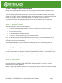
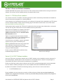
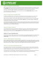
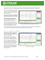
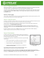
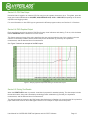
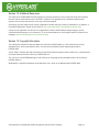
PCB CONTROLLED IMPEDANCE
ANALYZERS AND TEST SYSTEMS
User Manual for HL-PCB™ Version 1.2.x
Applies to Model Numbers
HL300S, HL3204
© 2014 - HYPERLABS, Inc.
Revision 1.2.0 | www.hyperlabsinc.com
Introduction
These consolidated reference materials apply to all PCB Controlled Impedance Analyzers and Test Systems from
HYPERLABS and the included HL-PCB™ software.
For further technical support, please visit our website: www.hyperlabsinc.com
Table of Contents
Section 1: Package Contents and Description ....................................................................................... 3
Section 1.1: Test System Contents .................................................................................................... 3
Section 1.2: USB Power and Control.................................................................................................. 3
Section 1.3: Static Protection ............................................................................................................. 3
Section 2: Driver and Software Installation............................................................................................. 4
Section 2.1: FTDI Device Driver Installation ....................................................................................... 4
Section 2.2: HL-PCB™ Software Installation ...................................................................................... 4
Section 2.3: Software Updates ........................................................................................................... 5
Section 3: Hardware and Software Initialization ..................................................................................... 5
Section 3.1: Warm-up Period ............................................................................................................. 5
Section 3.2: Software Startup and Initial Calibration ........................................................................... 5
Section 3.3: Data logging ................................................................................................................... 5
Section 4: Overview of HL-PCB™ Software Interface ............................................................................ 6
Section 5: Test Environment Setup ........................................................................................................ 7
Section 5.1: Waveform Plot Area........................................................................................................ 7
Section 5.2: Saving and Loading Test Environment Settings.............................................................. 7
Section 5.3: Data Acquisition Modes .................................................................................................. 7
Section 5.5: Using Continuous Acquisition Mode ............................................................................... 8
Section 5.6: Dielectric Constant (K) .................................................................................................... 8
Section 6.1: Setting Impedance Tolerance Range .............................................................................. 8
Section 6.2: Coupon Start and End Boundary Areas .......................................................................... 8
Section 7: Pass/Fail and Cursor Readings ........................................................................................... 10
Section 7.1: Pass/Fail Button ........................................................................................................... 10
Section 7.2: Pass/Fail Impedance Reading ...................................................................................... 10
Section 7.3: Cursor-based Measurements ....................................................................................... 10
Section 8: Differential and Single-ended Impedance Modes ................................................................ 11
Section 8.1: Odd-mode Differential Impedance ................................................................................ 11
Section 8.2: Even-mode Differential Impedance ............................................................................... 11
User Manual for HYPERLABS PCB Test Systems and HL-PCB™ Software
Page 1
Section 8.3: Single-ended Impedance .............................................................................................. 12
Section 9: Data Logging....................................................................................................................... 12
Section 9.1: Output File Locations .................................................................................................... 12
Section 9.2: Data Serialization ......................................................................................................... 12
Section 9.4: PNG Graphical Output .................................................................................................. 13
Section 9.5: Printing Test Results..................................................................................................... 13
Section 10.1: Quick Calibration ........................................................................................................ 14
Section 10.3: Annual NIST Certification............................................................................................ 14
Section 11: Additional Resources ........................................................................................................ 15
Section 12: Copyright Information ........................................................................................................ 15
User Manual for HYPERLABS PCB Test Systems and HL-PCB™ Software
Page 2
Section 1: Package Contents and Description
HYPERLABS Controlled Impedance Analyzers and PCB Test Systems are designed to simplify the process of
testing characteristic impedance in printed circuit board (PCB) applications.
These instruments use time domain reflectometry to take accurate and repeatable impedance measurements.
Although the HL-PCB™ software is included with both our stand-alone Analyzers (e.g. HL3204) and full PCB Test
Systems (e.g. HL300S), this manual was primarily written for use with our full PCB Test Systems.
Any references to HYPERLABS probes and other accessories found below will not apply to stand-alone
Analyzers if used with probes from other manufacturers.
Section 1.1: Test System Contents
Each PCB Test System consists of the following parts:
•
1 x HL32xx Controlled Impedance Analyzer (where “xx” is the number of instrument channels)
•
3 x Probes (see note below)
•
1 x HL9600 Calibration Standards Substrate
•
1 x HL-PCB™ software (Windows only) with free lifetime updates
NOTE: The standard configuration includes handheld pencil probes (HL9720 even-mode differential, HL9721
single-ended, and HL9722 odd-mode differential). If different probes were requested at time of purchase, the
configuration and product numbers will vary.
When purchased separately, the HL32xx Analyzers include only the HL-PCB™ software. Any probes and
accessories must be supplied by the end-user.
Section 1.2: USB Power and Control
All HYPERLABS instruments are powered and controlled via a single USB port. The included HL-PCB™ software
and drivers are compatible with all versions of Windows XP, Windows Vista, Windows 7, and Windows 8. At this
time, there are no plans for OS X, Linux, or other operating system support.
The instrument should always be plugged into the PC prior to running the HL-PCB™ software.
Section 1.3: Static Protection
Model number HL3204 is an electrostatic-robust (ruggedized) instrument, complaint with Class 2 of ESDS
Component Sensitivity Classification (ESD STM5.1-1998). Static protection is not required to use these
instruments for most desktop applications.
However, in particularly harsh test environments, we do recommend using an anti-static wrist strap (not included).
The wrist strap can be plugged directly into the labeled GROUND port of the instrument.
User Manual for HYPERLABS PCB Test Systems and HL-PCB™ Software
Page 3
Section 2: Driver and Software Installation
HYPERLABS PCB Test Systems utilize drivers from FTDI, which must be installed before running the HL-PCB™
software. If the drivers are not installed properly, the software will not work.
Section 2.1: FTDI Device Driver Installation
If an internet connection is available, the latest signed drivers will be automatically downloaded and installed as
soon the instrument is plugged in to a working USB port.
If the computer is not connected to the internet or not configured for automatic driver installation, the FTDI drivers
must be manually installed. Please visit the following page to download the latest version of the FTDI drivers:
http://www.ftdichip.com/Drivers/D2XX.htm
If the program states it cannot find “FTD2xx.dll”, download the driver package at the address above, extract the
.ZIP file, and copy the FTD2xx.dll file into the installation directory listed below.
When the driver installation is completed, the device
will show up in the Windows Device Manager as a
USB Serial Converter under the Universal Serial
Bus Controllers section.
Figure 1 at right shows the device when installed
correctly on a Windows PC. The HL3204 appears as
the highlighted item at the bottom of the list.
If the drivers are not installed, a generic description
appears next to a yellow exclamation point.
NOTE: HYPERLABS instruments may conflict with
other USB Serial Converter devices. Please
disconnect all other USB Serial Converters before
using your PCB Test System.
Please contact HYPERLABS for additional help
troubleshooting driver errors.
Figure 1: HL3204 shown as a USB Serial Controller in
Windows Device Manager
Section 2.2: HL-PCB™ Software Installation
Once the FTDI drivers are properly installed, the HL-PCB™ software can be installed by running “setup.exe” in
the install package, available either on the included CD or downloaded from the internet. If the package is in
compressed (.zip) format, all files must be extracted prior to installation.
Please note that each model number includes its own HL-PCB™ software package which can be downloaded
from our website. Software packages are not cross-compatible with other HYPERLABS instruments.
By default, the software will install to the following directory, where “HLxxxx” is the model number:
•
“C:\HYPERLABS\HLxxxx\”
During installation, the user may elect to install to a different directory. We do not recommend installing the
software in the “Program Flies” directories, as this may cause Windows permissions problems if the program is
not run as an administrator.
User Manual for HYPERLABS PCB Test Systems and HL-PCB™ Software
Page 4
Section 2.3: Software Updates
All HYPERLABS instruments include free lifetime software upgrades. The installed version is shown in the title bar
of the HL-PCB™ software, e.g. “HL-PCB for HL3204 (v1.x.x)”.
At this time, there is no auto-update utility built into the HL-PCB™ software. Please check our website regularly
for updated versions.
Section 3: Hardware and Software Initialization
HYPERLABS PCB Test Systems are designed for simple setup and use. While the instrument can be used in true
Plug-and-Play fashion, we recommend the following steps to improve measurement accuracy and repeatability.
If any problems are encountered at hardware or software startup, please contact HYPERLABS for additional
technical support.
Section 3.1: Warm-up Period
Like most test and measurement instruments, HYPERLABS PCB Test Systems benefit from a short warm-up
period prior to use. This ensures optimal accuracy in impedance readings.
To warm up the instrument, simply plug it into a USB port on any Windows PC for 10-15 minutes before testing
begins. The HL-PCB™ software does not need to be running during warm-up.
Alternatively, the PCB Test System may be left continuously connected to the USB port when not in use. This
keeps the instrument in a constant state of warm-up. There is no risk of damage from keeping the instrument
continuously plugged in. Power consumption is minimal, as is the case with all USB-powered devices.
Section 3.2: Software Startup and Initial Calibration
Each time the HL-PCB™ software is run, the program performs a quick calibration of all instrument channels. This
calibration, with typical accuracy of 0.5%, is performed on an internal reference cable in the housing.
During the calibration process, which usually takes 5-10 seconds, the software will not be responsive to user
input, instrument controls may flicker, and an orange button labeled NOT READY is shown in the top-right corner
of the screen.
When calibration is complete, a blue button labeled READY will appear in the top right corner of the screen.
Section 3.3: Data logging
Each time the HL-PCB™ software is run, a new CSV-formatted data log is created to store test results. Until the
software is closed, all logs will be stored in this file. The file name is based on the time stamp at startup, and is
shown the message box on the bottom right side of the HL-PCB™ screen after calibration.
The log file can be found in the program installation directory, e.g. “C:\HYPERLABS\HL3204\datalogs”.
At this time, the software cannot be configured to append new data to existing log files, and the only way to start a
new log file is to close and reopen the HL-PCB™ software.
User Manual for HYPERLABS PCB Test Systems and HL-PCB™ Software
Page 5
Section 4: Overview of HL-PCB™ Software Interface
When the HL-PCB™ software is running, the user will see a screen similar to Figure 2 below, which has been
marked up with colored arrows to highlight the important software features and controls.
Figure 2: Startup Screen for HL-TDR™ for HL1101, with Important Features Labelled
Detailed descriptions of the highlighted features and controls can be found in the following Sections:
1. Waveform Display Area, Section 5.1
2. Horizontal and Vertical Display Area Controls, Section 5.1
3. Coupon Pass/Fail Limits, Section 6
4. Acquisition / Logging Options, Section 5.3-5.5
5. Other Program Options, Sections 5.3, 10
6. Pass/Fail Button, Channel Selection, and Impedance Readings, Sections 7-8
7. Cursor Readings, Section 7.3
8. Product and Serial Number Information, Section 9
9. Data Logging and Output Controls, Section 9
10. User Information Panel, Section 11
User Manual for HYPERLABS PCB Test Systems and HL-PCB™ Software
Page 6
Section 5: Test Environment Setup
The HL-PCB™ software allows users to modify certain environmental variables and create a test setup that fits
their coupon testing needs. For further help determining the ideal test setup for your application, please review the
Application Guides on our website, or contact HYPERLABS.
Section 5.1: Waveform Plot Area
The HL-PCB™ software is pre-configured to show impedance, in Ohms, as a function of distance, in Feet. These
units cannot be changed by the operator.
By default, the waveform display area is optimized to display a standard 6-inch PCB test coupon, measured at the
end of HYPERLABS probes with 3-foot SMA cables. The operator can adjust the display window, both horizontally
and vertically, as required by the coupon and application.
Controls for adjusting window dimensions are found under Graph Area in the bottom-left corner of the software
interface. The minimum and maximum values allowed for each axis are as follows:
•
Horizontal: 0 to 15 ft (roundtrip)
•
Vertical: 0 to 500 Ohms
NOTE: The horizontal axis measurement includes the internal cabling of the instrument as well as any attached
probes and cabling. Accordingly, a distance reading greater than the length of the coupon is to be expected.
Section 5.2: Saving and Loading Test Environment Settings
To save time on common test procedures, the HL-PCB™ software allows the operator to save test environment
settings and retrieve them later. This is accomplished using the Settings menu in the program toolbar.
Clicking the Save Settings menu stores the following environmental variables: horizontal and vertical graph
window, coupon pass/fail limits, and dielectric constant (K). The user can select the file name, which will be a .hls
(HYPERLABS settings) file type.
To retrieve stored settings, choose the Load Settings menu and select the desired settings file. The Restore
Defaults menu option can be used to set all variables to the program defaults at any time.
Section 5.3: Data Acquisition Modes
The HL-PCB™ software offers two modes of waveform acquisition, manual (default) and continuous. It also
provides two data logging options, manual (default) and automatic.
To toggle between modes, simply check or uncheck the boxes labeled Continuous Acquisition and/or Log
Every Acquisition in the Acquisition / Logging section found in the bottom panel of the user interface.
Any logged data is saved to the CSV log file as described in Section 3.3 above. For additional information about
data logging, please see Section 9 below.
User Manual for HYPERLABS PCB Test Systems and HL-PCB™ Software
Page 7
Section 5.4: Using Manual Acquisition Mode
When manual acquisition mode is active, the operator may acquire waveforms individually on demand by clicking
the ACQUIRE button located on the right side of the user interface. Each time the button is pressed, a waveform
is acquired. If automatic logging is disabled, click the LOG button to save data to the active CSV file.
If automatic logging is enabled, the functions are combined into a single ACQUIRE AND LOG button, which
performs both functions simultaneously.
Section 5.5: Using Continuous Acquisition Mode
In continuous acquisition mode, a new waveform is automatically acquired and displayed every second. This
mode is useful for engineers looking to debug the device under test, as intermittencies are easier to spot.
When continuous acquisition mode is active, data logging can be either manual or automatic. In manual logging
mode, the data can be saved to a CSV log file by clicking the LOG button. If automatic logging is enabled, the
operator does not need to press any buttons.
NOTE: Continuous acquisition mode is more resource-intensive than manual mode, so the user interface may be
slow to respond. To speed up the software, we recommend disabling continuous acquisition while environmental
variables are set, then re-enabling it afterwards.
Section 5.6: Dielectric Constant (K)
As in all TDR-based instruments, the dielectric constant (K) of the device under test will impact the accuracy of
distance measurements. The default value in the HL-PCB™ software is set to 2.25. This value can easily be
adjusted using the control found in the Other Options portion of the bottom user interface panel.
Section 6: Coupon Pass/Fail Limits
Pass/Fail tests in the HL-PCB™ software are performed based on user-supplied specifications for impedance and
coupon length. Controls to adjust these limits are found under Coupon Pass / Fail Limits in the bottom user
interface panel.
Section 6.1: Setting Impedance Tolerance Range
Because PCBs are manufactured to different impedance specifications, it is important for the operator to set these
limits in the HL-PCB™ software. This can be done by setting upper and lower impedance bounds (in Ohms) in the
bottom panel of the user interface. The green and red boundaries will auto-size based on these values.
Section 6.2: Coupon Start and End Boundary Areas
In the waveform plot area, two sets of colored boundaries are used to identify the coupon and the area in which
measurements are taken. The outer green bounds represent the start and end of the coupon as specified by the
operator. Vertically, the bounds are based on the user-provided impedance tolerance.
As specified by IPC-2141A standards, characteristic impedance measurements are taken between the 50% and
70% points of the coupon. Accordingly, the inner red bounds are automatically placed at these points.
User Manual for HYPERLABS PCB Test Systems and HL-PCB™ Software
Page 8
Section 6.3: Determining the Coupon Start Point
The HL-PCB™ software is pre-configured to position the coupon start point at the end of the included probes. If
different probes are used, or the coupon length needs to be manually adjusted, please follow the steps below.
First, connect the appropriate probe to the
analyzer instrument and touch the Open
pads on the included HL9600 Calibration
Standard Substrate.
Next, acquire a waveform in the software.
Set the coupon start at the point where the
impedance reaches the top of the window.
This point can be seen in the example
Figure 3 at right. As seen here, the
coupon start point (left boundary of the
green line) has been set at 11.3 ft.
This is where the coupon would begin
during normal testing. Once set, automatic
software edge stabilization ensures that
the coupon start point does not move.
Figure 3: Coupon start location determined using the HL9600
Calibration Standard Substrate (old software version shown)
NOTE: At this time, the coupon start position is reset to default each time the software is opened. Accordingly, the
coupon start and end points should be verified at the beginning of each testing session.
Section 6.4: Locating the Coupon End Point
By default, the HL-PCB™ coupon width is
set to 6 inches (12 inches roundtrip),
which is the ideal coupon length specified
by IPC-2141A standards.
If the coupon under test is longer or
shorter than the standard, the coupon
position needs to be adjusted manually.
To do this, connect the probe to the
instrument and place it on the PCB to be
tested. Note the point where the signal
goes to open at the end of the coupon.
As shown in the example in Figure 4 at
right, the coupon end point (right green
bound) should be set where impedance
rises off the screen.
Figure 4: Coupon end point set at the point impedance rises to open
(old software version shown)
User Manual for HYPERLABS PCB Test Systems and HL-PCB™ Software
Page 9
Section 7: Pass/Fail and Cursor Readings
Once the coupon start and end points have even set as explained in Section 6 above, the HL-PCB™ software
can provide simple Pass/Fail and characteristic impedance readings.
Section 7.1: Pass/Fail Button
The button in the top-right corner of the user interface indicates a PASS or FAIL based on the waveform and the
limits specified (see Section 6 above). If any part of the waveform does not intersect either the red or green
bounds, the test will trigger a PASS. If it does intersect the bounds, FAIL will be shown.
Section 7.2: Pass/Fail Impedance Reading
The pass/fail test is performed based on the average impedance reading measured between the 50% and 70%
points on the coupon, as per IPC-2141A standards. For the operator’s convenience, this value is shown directly
below the PASS/FAIL button in the top-right corner of the user interface.
If the differential channel pair is active, this box will show the odd-mode differential impedance, labeled DIFF
Impedance [Ohm]. If either of the single-ended channels is active, this box will show a single-ended impedance
reading, labeled CH1+ or CH2+ Impedance [Ohm].
For information regarding the various impedance measurement modes available using the PCB Test System and
HL-PCB™, please see Section 8 below.
Section 7.3: Cursor-based Measurements
Two cursors, one red and one blue, are available for spot impedance or distance measurements. These cursors
can be dragged to any point on the waveform. The red and blue text boxes in the bottom-right corner of the user
interface show the numerical readings, as well as the distance between the cursors.
User Manual for HYPERLABS PCB Test Systems and HL-PCB™ Software
Page 10
Section 8: Differential and Single-ended Impedance Modes
PCB Test Systems from HYPERLABS with at least 4 channels are capable of measuring odd-mode differential,
even-mode differential, and single-ended impedance. To switch between these modes, simply connect the correct
probe and select the channels as indicated below.
The channel switching control can be found in the top-right corner of the user interface, just below the impedance
reading box.
The table shown in Figure 5 below provides a quick reference for the settings and probes required for each mode.
More details can be found in Sections 8.1-8.3 on the following page.
Probe Part Number
Channel Selection
How to read output
Odd-mode Differential
HL9722
Differential (DIFF)
Direct reading
Even-mode Differential
HL9720
CH1+ or CH2+
Multiply single-ended
reading by 2
Single-ended
HL9721
CH1+ or CH2+
Direct reading
Figure 5: Quick reference table of impedance measurement modes
Section 8.1: Odd-mode Differential Impedance
Odd-mode differential impedance is measured on a pair of transmission lines when driven by equal and opposite
polarity signals. A positive-going signal is transmitted through one line, while a negative-going signal is sent
through the other. The impedance readings are then added together to provide odd-mode differential impedance.
For most applications and industry standards, this provides the most useful reading of differential impedance.
To perform an odd-mode differential reading, connect an odd-mode differential probe (e.g. the HL9722) and set
the channel selector to DIFF. A direct odd-mode differential reading will be shown below the PASS/FAIL button.
Section 8.2: Even-mode Differential Impedance
Even-mode differential impedance is measured on a pair of transmission lines when driven by signals of the same
polarity and amplitude. A positive-going signal is transmitted through each line. The impedance readings are then
added together to provide even-mode differential impedance.
This mode is not as commonly used as odd-mode, but it can be useful in certain situations.
To perform an even-mode differential reading, connect an even-mode differential probe (e.g. the HL9720) and set
the channel selector to either single-ended channel (CH1+ or CH2+).
Currently, the reading shown below the PASS/FAIL button should be multiplied by two to provide a correct
reading. In future versions of the software, this will automatically be calculated and displayed.
User Manual for HYPERLABS PCB Test Systems and HL-PCB™ Software
Page 11
Section 8.3: Single-ended Impedance
Single-ended impedance is measured on an individual transmission lines when driven by a positive-going signal.
This mode is useful on non-differential lines as well as when specified by application needs.
To perform a single-ended reading, connect a single-ended probe (e.g. the HL9721) and set the channel selector
to either single-ended channel (CH1+ or CH2+). A direct single-ended impedance reading will be shown below
the PASS/FAIL button.
Section 9: Data Logging
The HL-PCB™ software offers numerical and visual data logging capabilities. Numerical data are saved to a CSV
file, while entire waveforms can be saved as PNG images.
Section 9.1: Output File Locations
On startup, the HL-PCB™ software creates a new unique log file in CSV format. The filename is shown in the text
box located in the bottom right corner of the user interface, and it cannot be changed.
If the HL-PCB™ software has been installed in the default location, the CSV data file will be located in the
following directory: “C:\HYPERLABS\HL3204\datalogs”
The filename will be derived from the timestamp, allowing the operator to distinguish between different test
sessions. For example, a file named “log_140130112255” would have been created on January 30th, 2014 at
11:22:55 AM.
By default, PNG files are saved to the “images” directory in the location where the HL-PCB™ software is
installed. Image files can be saved to any location on the computer.
Section 9.2: Data Serialization
HL-PCB™ make it easy to serialize and organize data when large batches of
test coupons are being analyzed at once. The image in Figure 6 at right shows
the data serialization options in the software.
For optimal data organization, HYPERLABS recommends using the following
data structure:
•
Serial: unique identifier for each PCB or other device under test
•
Rev: product revision, if testing different prototypes or versions
•
Product: internal or customer-supplied part number
•
Customer: company, department, individual, etc. for whom the
measurement is being taken
Figure 6: Example
Serialization Data and Log
File Location
All serialization fields are optional. If text is entered into the field, it will be
logged. Otherwise, the fields in the CSV log file will be left blank.
When the measurement is taken, a timestamp is also added to the log file to ensure that every acquisition is
recorded. Timestamps are formatted according to Year, Month, Day, Hour, Minute, and Second. For example, a
timestamp of “140130112255” would have been created on January 30th, 2014 at 11:22:55 AM.
User Manual for HYPERLABS PCB Test Systems and HL-PCB™ Software
Page 12
Section 9.3: CSV Data Output
Numerical data is logged to an external CSV file every time the operator chooses to do so. To log data, press the
large green button labeled either ACQUIRE, ACQUIRE AND LOG, LOG or LOG DATA, depending on the active
acquisition and logging modes.
For more information on how CSV logs are generated in different program modes, see Sections 5.3-5.4 above.
Section 9.4: PNG Graphical Output
Entire waveforms can also be saved to PNG files for easy visual reference and sharing. To do so, click the button
labeled SAVE PNG when a waveform is on the screen.
This feature saves an image of the entire waveform plot area, and excludes the rest of the controls in the user
interface. A timestamp is added, which contains the product serialization (if provided), the impedance
measurement, and the date and time of measurement.
See Figure 7 below for an example of the PNG output.
Figure 7: Sample graphical output while testing a 116 Ohm test coupon
Section 9.5: Printing Test Results
When the PRINT DATA button is pressed, visual data is prepared for standard printing. The data output includes
the waveform area, along with a timestamp containing product serialization (if provided), the impedance
measurement, and the date and time of measurement.
The data generated is identical to the PNG output described above in Section 9.4, except that the file is printed on
paper rather than stored on disk. See Figure 7 above for an example of output sent to the printer.
User Manual for HYPERLABS PCB Test Systems and HL-PCB™ Software
Page 13
Section 10: Instrument Calibration
Using the HL-PCB™ software, the HL3204 and other PCB Test Systems can be calibrated on-demand using two
different methods: Quick Calibration and External Calibration. For annual NIST certification, the HL3204, HL9600
calibration standards, and probes should be sent to HYPERLABS every year for full verification.
Quick Calibration is sufficient in most test scenarios, while External Calibration uses a network analyzer-style
calibration standard substrate for applications requiring greater accuracy.
Section 10.1: Quick Calibration
The Quick Calibration routine calibrates the instrument to an internal semi-rigid 50 Ω coax reference cable with
typical accuracy of 0.5%. This action is performed automatically at software startup, and repeats periodically
during normal instrument use.
Quick Calibration can also be triggered manually using the QUICK CALIBRATE button located along the bottom
panel of the software in the Other Options section.
Section 10.2: External Calibration
External calibration using the HL9600 Calibration Standards Substrate is an upcoming feature and is not available
as of HL-PCB™ v1.2.0.
Section 10.3: Annual NIST Certification
When used in applications requiring annual NIST certification, the full PCB Test System should be sent back to
HYPERLABS every year for full calibration and verification.
Please see our website for current pricing and policies related to annual NIST certification.
Section 11: User Information Panel
The user information panel found in the bottom-right corner of the program interface provides important
information to the test operator.
On startup, this panel shows the status of calibration and the log file to be used during the test session. When
subsequent calibration is performed, the status of that action is also indicated.
This panel also informs the user when a waveform is acquired (manual acquire mode only) and/or data is logged
to the active CSV file.
NOTE: In future versions of HL-PCB, this panel will be used for more robust information sharing and logging.
Please review this section with each new version release.
User Manual for HYPERLABS PCB Test Systems and HL-PCB™ Software
Page 14
Section 12: Additional Resources
This manual for HYPERLABS PCB Test Systems is primarily intended to cover instrument setup and familiarize
the user with the major features of the HL-PCB™ software. The applications for controlled impedance test
systems are too many and varied to cover fully in this User Manual.
Accordingly, we have made a wide variety of Application Guides and other reference materials on our website. A
full listing of Application Guides can be found at: http://www.hyperlabsinc.com/application-guides.aspx
If help for your application isn’t shown in our Application Guides, HYPERLABS is always happy to provide
unlimited technical support to our customers. For up-to-date telephone or email support options, please see our
webpage: http://www.hyperlabsinc.com/contact-us.aspx
Section 13: Copyright Information
The information contained in this User Manual is © 2014 by HYPERLABS, Inc. This manual may be freely
distributed as-is, but any translations, edits, or revisions are prohibited unless expressly approved by
HYPERLABS.
The HL-PCB™ software title and screenshots, and all instrument and system model numbers (e.g. HL3204) listed
in this User Manual are also © 2014 by HYPERLABS, Inc.
The “HL Circle” and HYPERLABS logo found at the top of each page of this User Manual are © 2012-2014 by
HYPERLABS, Inc.
Windows® is a registered trademark of the Microsoft Corp., which is not affiliated with HYPERLABS.
User Manual for HYPERLABS PCB Test Systems and HL-PCB™ Software
Page 15