1
MINI
DEVELOPMENT
BOARD
LPC
2129
make your own
intelligent embedded world . . .
USERS GUIDE
TABLE OF CONTENTS
1.0
2.0
3.0
OVERVIEW.............................................................................................................................. 2
1.1
CONTROLLER SPECIFICATION............................................................................. 3
1.2
KEY FEATURES...................................................................................................... 4
HARDWARE INTRODUCTION............................................................................................... 6
2.1
BLOCK DIAGRAM....................................................................................................
6
2.2
INTERFACE OVERVIEW.........................................................................................
7
2.3
PERIPHERAL DESCRIPTION.................................................................................. 8
2.4
JUMPER DESCRIPTION.......................................................................................... 9
2.5
POWER SUPPLY.....................................................................................................
2.6
CLOCK SOURCE...................................................................................................... 10
2.7
MICROCONTROLLER - PIN OUT............................................................................ 11
2.8
PORT EXPANDER.................................................................................................... 12
2.9
JTAG CONNECTION................................................................................................ 13
2.10
LED INTERFACING.................................................................................................. 14
2.11
LCD INTERFACING.................................................................................................. 15
2.12
PULL-UP KEYS INTERFACING................................................................................ 16
2.13
BUZZER INTERFACING........................................................................................... 17
2.14
UNIVERSAL ASYNCHRONOUS RECIEVER TRANSMITTER............................... 18
2.15
SERVO MOTOR........................................................................................................ 25
2.16
ANALOG TO DIGITAL CONVERTER POTENTIOMETER INTERFACE.................. 26
2.17
TEMPERATURE SENSOR INTERFACE.................................................................. 26
2.18
CONTROLLER AREA NETWORK............................................................................ 27
SOFTWARE DEVELOPMENT................................................................................................. 28
3.1
4.0
1
10
FAMILIARIZATION OF KEIL MICROVISION4.......................................................... 28
I/O PIN DISTRIBUTION.......................................................................................................... 42
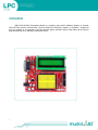
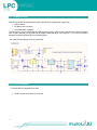
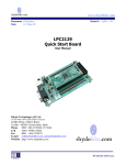
OVERVIEW
ARM LPC2129 Mini Development Board is a miniature and powerful hardware platform to evaluate
LPC2129 Flash memory microcontroller. The eCee ARM LPC2129 Board contains all hardware components
that are required in a single-chip LPC2129 controller system ,plus Mini USB or Serial Cable can be used for
programming ARM LPC2129 Mini Development Board.
2
1.1. CONTROLLER SPECIFICATION
1.
2.
3.
4.
5.
6.
7.
8.
9.
10.
11.
12.
13.
14.
15.
16.
17.
18.
19.
20.
21.
22.
23.
24.
16/32-bit ARM7TDMI-S microcontroller in a 64 or 144 pin package.
16 KB on-chip Static RAM
128/256 kB on-chip Flash Program Memory
128-bit wide interface/accelerator enables high speed 60 MHz operation.
External 8, 16 or 32-bit bus (144 pin package only)
In-System Programming (ISP) and In-Application Programming (IAP) via on-chip boot-loader software.
Flash programming takes 1ms per 512 byte line. Single sector or full chip erase takes 400ms.
Embedded-ICE-RT interface enables breakpoints and watch points.
Interrupt service routines can continue to execute whilst the foreground task is debugged with the onchip Real Monitor software.
Embedded Trace Macrocell enables non-intrusive high speed real-time tracing of instruction
execution.
2/4 interconnected CAN interfaces with advanced acceptance filters.
4/8 channel10-bit A/D converter with conversion time as low as 2.44 ms.
Two 32-bit timers (with 4 capture and 4 compare channels)
PWM unit (6 outputs), Real Time Clock and Watchdog.
Multiple serial interfaces including two UARTs (16C550), Fast I2C (400 kbits/s) and two
SPIs™.
60 MHz maximum CPU clock available from programmable on-chip PLL.
Vectored Interrupt Controller with configurable priorities and vector addresses.
Up to forty-six (64 pin) and hundred-twelve (144 pin package) 5V tolerant general purpose
I/O pins.
Up to 12 independent external interrupt pins available (EIN and CAP functions).
On-chip crystal oscillator with an operating range of 1 MHz to 30 MHz.
Two low power modes, Idle and Power-down.
Processor wake-up from Power-down mode via external interrupt.
Individual enable/disable of peripheral functions for power optimization.
Dual power supply.
• CPU operating voltage range of 1.65V to 1.95V (1.8V +/- 8.3%).
•
3
I/O power supply range of 3.0V to 3.6V (3.3V +/- 10%
1.2. KEY FEATURES OF ARM LPC2129 DEVELOPMENT BOARD-MINI
1.
2.
3.
4.
5.
6.
7.
8.
9.
10.
11.
12.
13.
14.
15.
16.
17.
18.
19.
20.
21.
22.
23.
24.
25.
26.
27.
28.
29.
30.
31.
32.
33.
34.
35.
4
Compact and ready to use design
On Board 10 MHz Crystal Oscillator
Integrated ARM LPC2129 Microcontroller
Professional EMI/RFI Complaint PCB Layout Design for Noise Reduction
High Quality Two layer PTH PCB
Multiple programming options – USB/RS-232 with jumper selection at UART0
No separate programmer required (Built in Boot loader)
Power indication LED (Red)
Multiple Power source (USB, RMC Connector, DC barrel jack) with jumper selection
Power Supply with Reverse Polarity Protection
Controller Area Network (CAN) transceiver
CAN Controller (MCP 2551) interface
CAN connection taken from RMC connector (+5V, CANH, CANL, GND)
Jumper selection at CAN RX & CAN TX
Buzzer interface
Pot interface to ADC
Temperature Sensor (MCP 9700) interface
For Buzzer,Temperature Sensor and Potentiometer jumper selection available, if necessary interface
independently
Servo motor(SIG,+5V,GND), LCD & ZigBee can be easily interfaced through on-board connectors
Potentiometer for contrast control
ZigBee can be interfaced from either side of the board at UART0
4 on-board switches including a RESET switch
3 on-board SMD LED s connected to port pins
SMD LEDs and Switches , if necessary interface independently
Breadboard can be attached to the board
5V and 3.3V regulators available
3.3V/5V output available in berg strips
External power supply and adapter having range of 7 – 9V DC
In UART0 communication, position of programmer switch should be in manual mode
UART0 available at RMC connector with jumper selection option for power i.e; 3.3V/5V
UART1 available on berg strip (GND,TXD1,RXD1)
Two on board programming modes
• Automatic - no reset, no ISP jumper
• Manual- insert ISP jumper & press reset switch
ISP jumper should be removed for code execution
On Board JTAG Connector for Debugging/Programming
All port pins available at Berg Strip
PACKAGE CONTENTS
5
•
Fully Assembled and Tested eCee ARM LPC2129 Mini Development Board
•
Software CDROM with
•
Schematic
•
Programming Software
•
Sample Hex Code
•
Example Codes
HARDWARE INTRODUCTION
The ARM LPC2129 Development Board (Mini) V1.01 is compatible with the LPC212X series of
microcontrollers. On board LPC2129 controller is available. The LPC212X series remains very popular as
general purpose microcontrollers, due to their industry standard instruction set, and low unit cost.
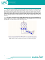
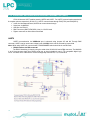
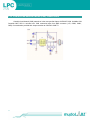
2.1. BLOCK DIAGRAM
6
2.2. INTERFACE OVERVIEW
Top view of the Development board -Mini
Bottom view of the Development board -Mini
7
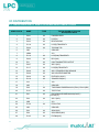
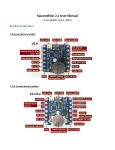
2.3. PERIPHERALS DESCRIPTION
8
PERIPHERALS
DESCRIPTION
ISP(J15)
ISP Connector,To program the IC
K6,K7
PORT pins on male berg strip
K1
USB Socket
K2
To select power source as USB/DC
K3
2 pin RMC connector for power
K4
DC barrel jack
K5
UART Interface via Female DB9 Connector
K14
RMC connector for 3V3/5V UART
K13
Servo connector pin
K8-K9-K10-K11
PORT pins on female berg strip
LED1-LED3
Light Emitting Diodes
PWR
Power indication LED
SW1-SW3
Pull-Up Switches
RESET(SW4)
Reset Button
PROGRAMMER(SW5)
To select Auto/ Manual mode of programming
LCD CONT (P1)
LCD Contrast control Pot
ADC (P2)
Potentiometer used as ADC input
U1
ARM LPC 2129
U2
LM7805(5V regulator IC)
U3
LD1117 (3V3 regulator IC)
U4
CP2102(USB interface)
U5
MAX232(Level converter)
U6
Temperature Sensor (MCP9700)
U7
Zigbee module connectors
U8
CP 2985(1.8V regulator)
U9
MCP 2551
IDC1
JTAG connector
BUZ1
Buzzer
LCD1
LCD
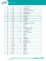
2.4. JUMPER SET DESCRIPTION
JUMPER
No.
DESCRIPTIONS
SET OPTIONS
SETTINGS
DESCRIPTION
Power Supply
Options
1-2
Select USB power
K2
2-3
Select external DC power
J16
UART0
Short to access
Select 3.3/5 V level for UART communication via
RMC connector
J12
Potentiometer
Short access
Enables ADC connection via POT
J11
Temperature Sensor
Short access
Enables temp sensor connection
J1, J2, J3
LED
Short access
Enables LED connection
J4,J5,J6
Pull-Up Key
Short access
Enables Pull-Up Key connection
J10
Buzzer
Short access
Enables buzzer connection
J8
JTAG
Short access
Establish J connection
J14,J1
CAN TX,RX
J7, J9
USART
9
Short to access
MCP 2551 (CAN controller)
1-2
RS232 Connection
2-3
USB Connection
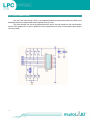
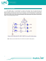
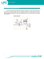
2.5. POWER SUPPLY
ARM LPC2129 Mini Development Board has 3 provisions for giving power supply input
• USB connector
• DC Barrel Jack Connector
• 2 Pin Male RMC Connector
The input source can be selected as DC/USB using the jumper. If DC source is selected, then either DC Barrel
Jack or RMC connector can be used and the supply voltage should be in the range of 7-12 V. Once the board is
powered, the power LED(red LED on the board) glows.
The external Power Supply circuit is given below:
2.6. CLOCK SOURCE
LPC2129 Mini Development Board uses
•
10
10 MHz crystal as the MCU clock source
2.7. MICROCONTROLLER - PIN OUT
11
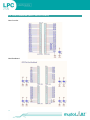
2.8. PORT EXPANDER (INPUT/ OUTPUT PORTS)
Near Controller
Near Breadboard
12
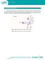
2.9. JTAG CONNECTION
The Joint Test Action Group (JTAG), is an integrated method for testing interconnects on printed circuit
boards (PCBs) that are implemented at the integrated circuit (IC) level.
The microcontroller can also be programmed and be used to test the operation of the microcontroller
with the JTAG programmer. In order to enable the JTAG programmer to be used, it is necessary to place jumper
J8 in the position
13
2.10. LED INTERFACING
LED’s are semiconductor diodes, electronic devices that permit current to flow in only one direction. The
diode is formed by bringing two slightly different materials together to form a PN junction. In a PN junction, the P
side contains excess positive charge ("holes") while the N side contains excess negative charge (“electrons”).
When a forward voltage is applied to the semi conducting element forming the PN junction, electrons move from
N area toward P area and holes move from P area toward N area. Near the junction, the electrons and holes
combine. As this occurs, energy is released in the form of light that is emitted by the LED. The material used in
the semi conducting element of an LED determines its color. LED’s are the simplest devices to test port
functioning.
LPC 2129 mini development board has 3 SMD LEDs connected to port pins P0.17, P0.18 & P0.19 via
jumpers J1 , J2 & J3. If any jumper is left open, then the corresponding port pin can be used independently. The
LEDs turn ON when the port pins are at logic high state and they get turned OFF when the port pins are at
logic low state. Each LED is interfaced via a current limiting resistor.
Note: Remove J1,J2 & J3 when P0.19,P0.18 & P0.17 are used for other purpose.
14
2.11. LCD - LIQUID CRYSTAL DISPLAY
The display is a standard 16x2 LCD which displays 2 lines of 16 characters. Each character is
40 pixels, making it 1280 pixels overall. The display receives ASCII codes for each character at the
data inputs (D0–D7). The data is presented to the display inputs by the MCU, and latched in by
triggering the E (Enable) input. The RW (Read/Write) line can be tied low (write mode), as the LCD is receiving
data only. The RS (Register Select) input allows commands to be sent to the display. RS selects
command/data mode. The display itself contains a microcontroller; the standard chip in this type of
display is the Hitachi HD44780. It must be initialized according to the data and display options required.
The module can be used 4-bit or 8-bit mode. The development board uses 4-bit interface. Data pins are P1.20P1.23 and control pins are P1.17(RS),P1.18(R/W) and P1.19(E). LCD contrast can be adjusted by using the
potentiometer.
15
2.12. PULL-UP KEYPAD
The simplest input to a microcontroller is a switch or push button. This can operate with just one
additional support component, a pull-up resistor. The board has 3 externally pulled up switches (SW1,SW2 &
SW3) connected to port pins P0.14, P0.15 & P0.16 via jumpers J4, J5 & J6 respectively. On shorting these
jumpers, the switches can be used as general pull-up keypad and if the jumpers are left open, then the port pins
can be used for other purposes. When the key is pressed, it connect the input pin to the ground via a small value
resistor. Thus input pin get logic low value.
Note : Remove J4,J5,J6 when P0.14, P0.15 & P0.16 are used for other purpose.
16
2.13. BUZZER INTERFACING
Buzzer is a simple I/O device. Normally we use piezo electric element as buzzer. Buzzer is driven using
a simple NPN transistor with biasing. The transistor’s base is connected to P0.21 of the microcontroller via
jumper J10. If the port pin is configured as output pin and logic high, the transistor will be triggered on which
in turn switch on the Buzzer. If logic low is provided, the buzzer will be turned off.
Note : Remove J10 when P0.21 is used for other purpose
17
2.14. UNIVERSAL ASYNCHRONOUS RECEIVER TRANSMITTER (UART)
LPC2129 has two UART modules namely UART0 and UART1. For UART0 communication transmission
& reception pins are respectively P0.0 & P0.1. UART1 communicates through P0.8(TXD1) and P0.9(RXD1).
• In the mini development board, UART0 can communicate through
• Serial port via MAX232
• USB port via CP2102
• RMC connector (GND,TXD0,RXD0, Vout) in 3.3V/5V levels
• Zigbee connectors on either side of the board
UART0
UART0 communication via USB/Serial port is selected using jumpers J7 and J9. Through RMC
connector, UART0 can be used in two voltage levels of 3V3/5V which can be selected by jumper J16.
Note: While using UART0 for communication, PROGRAMMER switch should be in manual mode
• RS232 Interface via DB9 connector
The RS232 interfacing is done by using the serial driver IC MAX 232 and a DB9 connector. The MAX232
is an IC that converts signal from RS232 serial port to signal suitable for use in TTL compatible digital logic
circuit. The MAX 232 is a dual driver/ receiver and typically converts RX, TX,CTS and RTS
18
•
USB Interface using CP2102
The CP2102 is a highly-integrated USB-to-UART Bridge Controller providing a simple solution for
updating RS-232 designs to USB using a minimum of components and PCB space.The CP2102 includes a USB
2.0 full-speed function controller,USB transceiver,oscillator ,EEPROM,and asynchronous serial data bus (UART)
with full modem control signals in a compact 5x5 mm MLP-28 package. No other external USB components are
required.
•
3V3 /5V UART0
Note: Short J7 & J9 while using 3V3 UART. Remove J1&J2, when you connect 3V3 UART
19
•
Zigbee Module Interfacing
ZigBee is a wireless networking standard that is aimed at remote control and sensor applications which is
suitable for operation in harsh radio environments and in isolated locations.ZigBee technology builds on IEEE
standard 802.15.4. Rhydolabz ARM LPC2129 mini development board zigbee interfacing can be done from
both bottom and top of the board. Communication with the ZigBee module uses a standard UART interface
compatible with 3V3.
Note: Remove jumpers J7&J9, while using Zigbee.
UART1
20
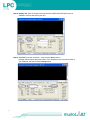
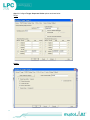
USING REALTERM IN PC
The RealTerm Software
The serial data transmitted through UART can be viewed on a PC using the realterm software.
The following section provides step by step tutorial of serial communication using realterm software. The
realterm software can be downloaded from http://realterm.sourceforge.net/
Step 1 : Open realterm software from Windows Start menu
21
All Programs
Real Term
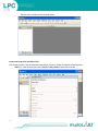
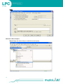
Step 2: Display Tab- Here the output text format selected is ANSI and Half Duplex mode is
enabled to view the data sent by the user.
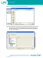
Step 3: Port Tab-To test the connection - make sure the Open button is
pressed, Select required baud rate and the “Port” dropdown here, select the number of
your COM port and then press the Change button.
22
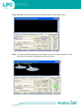
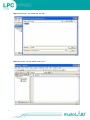
Step 4: Send Tab- Insert the desired data to be transmitted and press "Send ASCII" button.
Step 5 : The output after data transmission to the controller is shown in the following diagram. The text
sent by user and controller is highlighted by callouts in the figure.
23
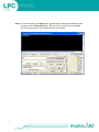
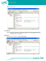
Step 6: To check reception, go to Send option, type the string in the space provided(encircled
in green) and click Send ASCII button. The first "hello" in green color is transmitted
from PC & that in yellow color is retransmitted by the controller
24
2.15. SERVO MOTOR INTERFACING
Servos are small mechanical motorized devices whose sole purpose is to rotate a tiny shaft attached to
a servo wheel in a specified position. Servos are controlled by sending a pulse width signal from an external
electronic device that generate PWM signal values. PWM signal send to the servo are translated into position
values by electronics inside the servo. In the mini development board, servo is connected to P1.24 with jumper
connection at K13.
25
2.16. ADC POTENTIOMETER INTERFACING
LPC 2129 mini development board has a potentiometer connected to its ADC pin P0.29 (channel2) via
jumper J12.
.
Note : Remove J12 when P0.21 is used for other purpose
2.17. TEMPARATURE SENSOR INTERFACING
MCP 9700 temperature sensor can be used to measure temperature. It is connected to P0.28(channel
1) via jumper J11. .
26
2.18. CONTROLLER AREA NETWORK (CAN) TRANSCEIVER
Controller Area Network (CAN) transceiver is the most peculiar feature of ARM LPC2129 .Available CAN
Controller MCP 2551 in on-board mini .CAN connection taken from RMC connector (+5V, CANH, CANL,
GND) .Communication provided with Jumper selection at CAN RX & CAN TX.
27
SOFTWARE DEVELOPMENT
3.1. FAMILIARIZATION of Keil µVision4
CREATING A PROJECT
µVision4 is a standard Windows application and started by clicking on the program icon. µVision4 includes
a project manager which makes it easy to design applications for an ARM microcontroller. You need to perform
the following steps to create a new project:
•
Open Keil µVision4 from start menu or Desktop shortcut
•
Create new Project File and Select CPU.
•
Create New Source Files.
•
Add Source Files to the Project.
•
Set Tool Options for Target Hardware.
•
Configure the CPU Startup Code.
•
Create a HEX File.
•
Build Project and Generate Application Program Code.
The section provides a step-by-step tutorial that shows you how to create a simple Keil µVision4 project.
Launch Keil µVision4
28
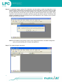
The Keil µVision window opens as shown below
Create new Project File and Select CPU.
This section provides a step-by-step tutorial that shows you how to create a simple Keil µVision4 project.
Step1 :To create a new project, select Project > New µVision Project from menu bar
29
Step 2 : Save the project in a suitable location with appropriate name
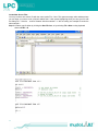
Step 3:The following window opens. When you create a new project Keil µVision4 asks you to select a
CPU for your project. The Select Device dialog box shows the µVision4 device database. Just
select the microcontroller you use. For the example in this chapter we are using the ARM
LPC2129 controller. Select LPC 2129 (listed under NXP) from the drop-down list and simplifies
in this way the tool configuration ,
30
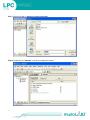
Step 4: An embedded program requires CPU initialization code that needs to match the configuration of your
hardware design. This Startup Code depends also on the tool chain that you are using. Since you might
need to modify that file to match your target hardware, the file should be copied to your project folder.
For most devices, Keil µVision4 asks you to copy the CPU specific Startup Code to your project. This is
required on almost all projects (exceptions are library projects and add-on projects). The Startup Code
performs configuration of the microcontroller device and initialization of the compiler run-time system.
Answer with YES to this question.
Note:The CPU Startup Code typically requires some configuration;however the default configuration
gives you a good starting point for single chip applications.
Step 5: This creates a target to the project
31
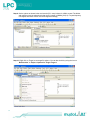
Create New Source Files
You may create a new source file with the menu option File – New. This opens an empty editor window where
you can enter your source code. µVision3 enables the C color syntax highlighting when you save your file with
the dialog File – Save As… under a filename with the extension *.c. We are saving our example file under the
name sample.c
Step 6: Create a new file either by clicking the New File icon, or by selecting File > New or using keyboard
shortcut CTRL + N
32
Step 7: Save the file with .c extension in the project folder
Step 8: Double click on “Startup.s” to open the configuration window
33
Step 9: Set the options as shown below and save the PLL setup is done for 10MHz crystal. The divider
and multiplier must be selected such that the PLL output is 30MHz((10/2)*6). If crystal frequency
is changed, then these values must be changed accordingly
Step 10: Right click on Target1 to set target file options. You can also do this by using the icon on
‘Build toolbar’ or Project > Options for Target ‘Target 1
34
Step 11: Configure Target, Output and Linker options as shown below
Target
Output
35
Linker
Add Source Files to Project
Step 12: Right click Source Group 1 to add C file to source group
36
Step 13: Select the C file created and cilck Add
Step 14: Now the c file gets added to the Source
37
Step 15: Type the code
Create HEX File
Step 16: Click the build icon (encircled in figure) to build the project. Errors (if any) get listed in the
Build output window. Correct them and build again. On successful building, the hex file will
be generated in the project folder
Build Project
Build option can be taken from Project > Build Target.
38
Now the corresponding hex file of the program will be generated inside the working folder in the name of the
project that we created. When you build an application with syntax errors, Keil µVision4 will display errors and
warning messages in the Build page/Build output . A double click on a message line opens the source file on
the correct location in the Keil µVision4 editor window. In this example the Hex file is Sample.hex. This file will
be available in the folder Sample.
SETTING UP ARM LPC2129 mini
Now the code can be flashed to the controller in the board,
Note the following jumper connections
• Select the power source as USB cable or DC source
• Select USB or serial port using jumpers J7 & J9 for flashing the code
Both jumpers on bottom side means USB programming
Both jumpers on top side means RS232 serial programming
• Select mode using programmer switch
In manual mode, insert ISP jumper and press reset button before programming
In auto mode, leave it open and proceed to programming
39
PROGRAMMING STEPS
Now power up the board. The power LED(red LED on the board) glows. Open Flash Utility. Select the correct
COM port recognized by PC and if its more than COM5 change it to any any lower COM port in Device Manager
and select any suitable baud rate. Also select XTAL Frequency as 10000kHz
Step 17: Open the desired hex file
40
Step 18: Read device ID
If auto mode is selected, simply clicking the ‘Read device ID’ button will read the ID. But in
manual mode, press reset switch and click
Step 19: Click ‘Upload to Flash’
After successfully flashing the code into the controller, remove ISP jumper if programmed using manual mode
and reset the board. Also ensure that all the necessary jumpers to get the desired output are shorted.
41
I/O DISTRIBUTION
4.1. PIN DISTRIBUTION OF ARM LPC2129 MINI DEVELOPMENT BOARD
42
ARM LPC2129
NAME
TYPE
THE I/O ASSIGN OF LPC2129
Development Board
1
P0.21
I/O
PWM5/BUZZER
2
P0.22
I/O
LCD(D1)
3
P0.23
I/O
RD2/CAN RXD
4
P1.19
I/O
LCD(E)/TRACEPKT3
5
P0.24
I/O
TD2/CAN TXD
6
VSS
-
GROUND
7
VDDA
-
3V3
8
P1.18
I/O
LCD(R/W)/TRACEPKT2
9
P0.25
I/O
RD1/(N/C)
10
TD1
I/O
CAN TRANSMITTER OUTPUT
11
P0.27
I/O
AD0.1/(N/C)
12
P1.17
I/O
LCD(RS)/TRACEPKT1
13
P0.28
I/O
AD0.1/TEMPERATURE SENSOR
14
P0.29
I/O
AD0.2/POTENTIOMETER
15
P0.30
I/O
EINT3/AD0.3/(N/C)
16
P1.16
I/O
TRACEPKT0/(N/C)
17
V18
-
1V8
18
VSS
-
GROUND
19
P0.0
I/O
TXD0/PWM1/ZIGBEE/MAX232(T2IN)/ CP2102(RX)
20
P1.31
I/O
TRST/JTAG
21
P0.1
I/O
22
P0.2
I/O
SCL0 /(N/C)
23
VDD
-
3V3
24
P1.26
I/O
RTCK/JTAG
25
VSS
-
GROUND
26
P0.3
I/O
SDA0/(N/C)
27
P0.4
I/O
SCK0/AD0.6/(N/C)
28
P1.25
I/O
EXTIN0/(N/C)
RXD0/PWM3/ZIGBEE/MAX232(R20UT) /
CP2102(TX)
43
29
P0.5
I/O
MISO0/AD0.7/(N/C)
30
P0.6
I/O
MOSI0/(N/C)
31
P0.7
I/O
PWM2/SSEL0/(N/C)
32
P1.24
I/O
SERVO MOTOR/TRACECLK
33
P0.8
I/O
TXD1/PWM4
34
P0.9
I/O
RXD1/PWM6/EINT3
35
P0.10
I/O
RTS1/(N/C)
36
P1.23
I/O
LCD(D7)
37
P0.11
I/O
CTS1/(N/C)
38
P0.12
I/O
DSR1/(N/C)
39
P0.13
I/O
DTR1/(N/C)
40
P1.22
I/O
LCD(D6)
41
P0.14
I/O
DCD1/EINT1/SWITCH SW1/ISP
42
VSS
-
GROUND
43
VDD
-
3V3
44
P1.21
I/O
LCD(D5)
45
P0.15
I/O
R11/EINT2/SWITCH SW2
46
P0.16
I/O
EINT0/SWITCH SW3
47
P0.17
I/O
SCK1/LED1
48
P1.20
I/O
LCD(D4)/TRACESYNC
49
V18
-
1V8
50
VSS
-
GROUND
51
VDD
-
3V3
52
P1.30
I/O
TMS/JTAG
53
P0.18
I/O
MISO1/LED2
54
P0.19
I/O
MOSI1/LED3
55
P0.20
I/O
EINT3/SSEL1/(N/C)
56
P1.29
I/O
TCK/JTAG
57
RESET
-
RESET
58
VSSA-PLL
-
GROUND
59
VSSA
-
GROUND
60
P1.28
I/O
TDI/JTAG
61
XTAL2
-
CRYSTAL
62
XTAL1
-
CRYSTAL
63
V18A
-
1V8
64
P1.27
I/O
TD0/JTAG
TECHNICAL SUPPORT
If you are experiencing a problem that is not described in this manual, please contact us.
Our phone lines are open from 9:00 AM – 5.00 PM (Indian Standard Time) Monday
through Saturday excluding holidays. Email can be sent to [email protected]
DISCLAIMER
Copyright © Rhydo Technologies (P) Ltd.
All rights are reserved. Reproduction in whole or in part is prohibited without the prior written consent of the
copyright owner. The information presented in this document does not form part of any quotation or
contract, is believed to be accurate and reliable and may be changed without notice.
Contact Us
Rhydo Technologies (P) Ltd.
(An ISO 9001:2008 Certified R&D Company)
Golden Plaza, Chittoor Road, Cochin – 682018, Kerala, India.
Tel: 0091 484 2370 444, 2371 666, Cell: 0091- 99466 70444
Fax: 0091 484 237 0579, Email: [email protected], [email protected]
For more information please visit: www.rhydolabz.com