1
Version 1.00
Getting Started with the SDCC/MetaLink 8051 C Cross
Compiler/Assembler and the XS 40 Prototyping Platform-- a
User’s Guide*
by
B. Earl Wells
Sin Ming Loo
Electrical and Computer Engineering Department
University of Alabama in Huntsville
Introduction
The purpose of this manual is to act as an aid to CPE 495, Computer Engineering Senior
Design I, students who will be using the embedded processor on the XS 40 reconfigurable prototyping platform to rapidly prototype a design that is implemented using both digital hardware and software components. This manual supplements the existing documentation on the XS 40 [1,2] and on
MetaLink Corporation’s embedded 8051 cross assembler, and the SDCC C cross compiler [3,4]. A
coordinated set of examples is presented that will take the user through the most common steps necessary for program entry, assembly/compilation, linking/locating, and software downloading onto
the XS 40 reconfigurable prototyping platform. To illustrate multiple design solution methodologies
and hardware/software trade-offs these design examples are the same ones that were presented in
the manual Getting Started with Xilinx Design Tools and the XS40 Rapid Prototyping Platform Version 2 [2]. This manual is divided up into six chapters as outlined below:
Chapter 1: General information is presented about the XS 40 platform, and the hardware
software codesign process. The hardware configuration of the Xilinx FGPA on
the XS 40 rapid prototyping platform that must be present to activate the 8031
microcontroller is also presented.
*This
material is based upon work supported by the National Science Foundation under Grant No. 9751482. Any opinions, findings,
and conclusions or recommendations expressed in this material are those of the authors and do not necessarily reflect the views of the
National Science Foundation.
1
Version 1.00
Chapter 2: A simple four bit binary counter design example is introduced. The added
logic needed to implement the memory mapped LED output latch is
presented. Both assembly language and C programming language solutions
are highlighted.
Chapter 3: A four bit binary to seven segment LED design example is introduced. The
added logic needed to implement the memory-mapped four-bit input latch is
presented. This latch is connected directly to the parallel port that comes
from the host PC. As with the previous chapter, both assembly language and
C programming language solutions to the binary to seven segment converter
problem are introduced.
Chapter 4: A hexadecimal counter is constructed by combining software modules from
the previous two designs. Both assembly language and C programming
language solutions are introduced.
Chapter 5: In this chapter, four hybrid hardware/software solutions to the hexadecimal
counter are introduced. These solutions all have one major component that is
present in the FPGA hardware while the other major component of the
design is present in the 8031 software. Design examples include the cases
where the binary to hexadecimal conversion is performed in the FPGA
hardware and the binary counter is implemented in the 8031 software and the
cases where the binary to hexadecimal conversion is performed in 8031
software and the binary counter is implemented inside the FPGA (both
polled and interrupt driven solutions to the second scenario are presented). In
all design examples both assembly language and C programming language
solutions are shown.
Chapter 6: References
2
Version 1.00
Chapter 1: The XS 40 and the SDCC and the MetaLink Set of
Embedded System Design Tools
The purpose of hardware/software codesign is to provide an integrated way for designing
hardware and software. Thus one starts from a system description that is not biased towards either
hardware or software which is then refined into separate software and hardware components. The
decision about which parts go into hardware and which into software (a process called partitioning) is done by estimating the performance of the system on the system model level and the
amount of system resources each implementation will take. The advantage of this paradigm is that
makes it possible to fully explore the design space and find a near optimal solution to the design
problem. In CPE 495, formal hardware/software codesign techniques will not be presented in
great detail, but rather the fundamental design issues in the hardware/software design process will
be introduced with the XS40 board being used as the rapid prototyping platform.
The XS 40
The XS 40 has many features that facilitate experimentation in hardware/software codesign as well as the general rapid prototyping of digital logic. The major component of this rapid
prototyping environment is the XS 40 board (version 1.4). This board is designed and produce by
X Engineering Software Systems Corporation (XESS). The XS 40 is a small rapid prototyping
board containing both a Xilinx XC4010XL FPGA and an 8031 type microcontroller (a ROM-less
version of 8051 -- in fact, throughout this document, 8031 and 8051 will be used interchangeably). The Xilinx XC4010XL FPGA has 400 Configurable Logic Blocks (CLBs, Xilinx’s logic
cell name) which is equivalent to 1,120 flip-flops. The 8031 type microcontroller is a derivative of
Intel’s 8051 series of microcontrollers. The board also contains a 100 MHz programmable oscillator for use with the microcontroller and user supplied logic that resides within the Xilinx FPGA.
Most of the I/O pins are directly connected with the XC4010XL FPGA -- these connections are
detailed in Appendix A of reference [2]. There is also 32K of SRAM present on the XS 40 for
storing 8031’s code/data (and other uses). The XS 40 board communicates with the PC via the
parallel port. This parallel port is used to download both the bit-stream information to the FPGA
and Intel hex format information to the 8031 microcontroller.
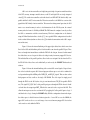
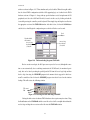
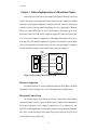
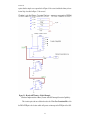
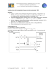
Figure 1.1 shows the block diagram of XS 40 prototyping environment that will be used in
CPE 495 this term.
3
Version 1.00
Programmable
Oscillator
7-Segment
Parallel Input Port From PC
100 Mhz
P/S 2 Port
Maximum
VGA
Port
8031
P0
A0-A7
D0-D7
P2
A8-A14
R/W
OE
CS
P1 P3
PSEN
ALE
RST
XTAL1
XC4010XL FPGA
32KB RAM
Figure 1.1: Block Diagram of the XS 40 Board.
A complete schematic of this board and the UAH added external circuity is presented in
the manual Getting Started with Xilinx Design Tools and the XS40 Rapid Prototyping Platform
(Version 2) [2].
HW/Software Codesign Paradigm
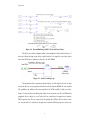
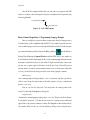
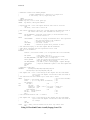
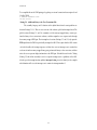
The Hardware/Software Codesign design flow is shown in Figure 1.2.
Fully Specify the Design
Decompose the Design into Functional Modules
Partition (Assign) the Modules to
Hardware (FPGA) and to Software (microcontroller)
Implement some of
the Functional Modules
in Software using C or
Assembly Language
and generate a
*.HEX file
Implement some of
the Functional Modules
in Hardware using
VHDL, Verilog, or
Schematic Capture and
generate a *.BIT file
Use the GXSLOAD
utility to rapidly
prototype both
portions of the design
on the XS40
XS40 Board V 1.4
Figure 1.2: The General Hardware/Software Design Flow on the XS 40
4
Version 1.00
The following outlines the general design process that is shown in Figure 1.2:
1.
Specifications of Design
The requirements to implement the design must first be fully understood and translated into a set of detailed specifications.
2.
Decomposition of Problem into Functions--I/O Definitions
The specifications are translated further in a manner that allows the problem to be
decomposed into functional modules with the inputs/outputs of each module being
clearly identified.
3.
Function/Task Allocation and Partitioning (FTAP)
This part of design process involves partitioning the problem into separate hardware/
software components. Comprehensive guidelines for this part of design process can
be very complex and are beyond the scope of this document. A general rule-ofthumb is to implement simple control type portions of the design that require fast/
frequent response time in hardware (the FPGA in this case) and implement more
complex decision making functions in software (using the microcontroller).
4.
The Implementation Phases
4.1. Xilinx Foundation 3.1i
In this phase of design process, hardware description languages (such as VHDL) and
schematics capture techniques can be used to enter the hardware portion of the
design. Then the Xilinx Foundations 3.1i CAD tool is used to generate the bit-image
for downloading to the FPGA.
4.2. C/Assembly coding
In this phase of the design, the embedded system’s software portion of the design is
entered using a combination of high-level language and assembly language techiqniques. Tasking Corporation’s C-cross compiler and 8031 cross assembler are used
to generate the hex-record file object code file which is then used to program the
8031 during the download process.
5.
Downloading
This is the phase where the design is actually implemented on the XS40 board. The
GXSLOAD downloading facilities are used to download in a seamless manner both
the FPGA bit-image file and the 8031 Intel hex-files which were produced in Step 4
of this process.
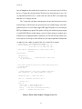
Basic FPGA Configuration to Support 8031 Operation
The following represents the basic FPGA configurations that are needed to support the
8031 execution of code that has been loaded into the 32K SRAM. In this section it is assumed that
the user is familiar with the Xilinx Foundation Series of design tools and that he or she is able to
enter the following schematics and create the associated bit map file that will be downloaded into
the XS 40 rapid prototyping platform. It is also sometimes assumed that the user started with a
project name of swbcount and that the project is located on the students X: drive.
5
Version 1.00
8031 series of microcontrollers are highly integrated single chip microcontrollers with an
8-bit CPU, memory, interrupt controller, timers, serial I/O and digital I/O on a single integrated
circuit [5]. The actual microcontroller used in this board is an OKI 80C154S which is fully compatible with Intel’s 80C31 microcontroller. This microcontroller is the ROM-less version of the
popular Intel 8051 family of microcontrollers. This means that during normal operation, the 8031
must access external memory in order to fetch instructions. In the XS 40 system, the external
memory takes the form of a 32 kilobyte SRAM. The FPGA must be configured correctly to allow
the 8031 to communicate with the external memory. This basic configuration can be obtained
using the Xilinx Foundation Series of tools [6,7]. An acceptable FPGA configuration is described
in the text that follows (students are directed to [5] for further documentation on the 8031 component architecture).
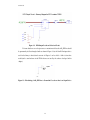
Figure 1.3 shows the internal buffering of the upper eight address lines which come from
Port 2 of the 8031 and the buffering of the 8 data bits which come from the parallel PC port. These
lines are brought into internal busses within the FPGA. In the designs, discussed in this manual
the address lines are used as part of address decoding circuitry for memory mapped I/O devices.
The individual bits of the parallel port lines allow for the user to input 8 bit data from the PC to
the XS 40. Each of these lines can be individually set and reset by the XSPORT Windows-based
software.
Figure 1.4 shows the internal buffering of the various 8031 control signals. Of special note
here is the fact that the separate 8031 data and program address spaces are in effect combined for
read operation through the ANDing of the PSEN_IN_ and RD_IN_ signals. This was done so that
both program and data could use the single 32K SRAM. The clock signal is simply passed
through the FPGA to the 8031 (where it is given an internal name CLK_IN for possible FPGA
use). The signal PC_D_IN5 (bit 5 of the parallel port) passes through the FPGA where it is buffered and drives the output signal RST_SW which is connected to the reset pin of the 8031. This
allows the microprocessor to be reset from the PC by toggling bit 5 of the parallel port to a logic 1
and then back to a logic 0 using the XSPORT utility. With the configuration shown in the figure
the address space is divided into two distinct regions the -- lower 32K accesses the SRAM, the
upper 32 K can be used to access a wide range of user created memory-mapped I/O devices that
can be made to reside within the FPGA.
6
Version 1.00
IPAD
PC_D_IN0
PC_D_IN1
PC_D_IN2
PC_D_IN3
PC_D_IN4
PC_D_IN5
PC_D_IN6
PC_D_IN7
IPAD
A_IN8
A_IN9
A_IN10
A_IN11
A_IN12
A_IN13
A_IN14
A_IN15
Figure 1.3: Internal Buffering of Parallel Port Lines and 8031 Upper Address Lines
7
Version 1.00
CLK_IN
A_IN15
CE_
PSEN_IN_
IN_OE_
OE_
RD_IN_
PC_D_IN5
RST_8031
Figure 1.4: Internal Buffering of 8031’s Clock and Control Lines
The 8031 series of microcomputers utilize a time multiplexed address/data bus. Figure 1.5
shows the address latching circuit that is required in order to decouple the lower eight address
lines. In the XS 40, these eight lines go directly to the 32 K SRAM.
from FPGA
to SRAM
(address bus)
ALE_IN_
Figure 1.5: Address Latching Logic
The introduction of the components shown in Figure 1.6 will complete the basic circuitry
need by the 8031 to execute programs which have been loaded into the SRAM. Of course without
I/O capabilities, the addition of the microcontroller to the XS 40 would be of little or no value.
Figure 1.6 shows the basic bus driving logic which is used to interface the 8031 to FPGA-based
peripherals. Devices which are “read” by the 8031 are considered to be output devices from the
FPGA’s point of view. They are connected to the eight bit AD_OUT bus. Devices that are “written” to by the 8031 are considered to be input devices from the FPGA’s perspective and are to be
8
Version 1.00
connected to the AD_IN bus. In the examples which follow this logic is used to interface the
LED’s and the parallel port input bits to the 8031.
Port
AD_SEL
Figure 1.6: Internal 8031 Address/Data Buss Driving Logic
To interface to the 8031 and SRAM on the XS 40, all pins must be locked to specific I/O
locations on the Xilinx FPGA. These locations are shown in the User Constraints File presented
in Listing 1.1. It should be noted that the circuitry needed to drive the AD_SEL, which controls
the direction that data flows into and out of the FPGA through the lower half of the multiplexed
address bus, is not present. This circuitry is presented in the next two chapters. Obviously, one
would need to incorporate this circuitry before a valid bit file can be created.
9
Version 1.00
NET CLK LOC=P13; # CLOCK FROM PROGRAMMABLE EXTERNAL OSCILLATOR
#
NET RST_8031 LOC=P36; # Reset pin driving 8031 coming out of FPGA
#
# DATA BITS FROM THE PC PARALLEL PORT
NET PC_D<0> LOC=P44;
NET PC_D<1> LOC=P45;
NET PC_D<2> LOC=P46;
NET PC_D<3> LOC=P47;
NET PC_D<4> LOC=P48;
NET PC_D<5> LOC=P49;
#
# MICROCONTROLLER PINS
NET XTAL1 LOC=P37; # 8031 CLOCK INPUT
NET ALE_ LOC=P29; # ACTIVE-LOW ADDRESS LATCH ENABLE
NET PSEN_ LOC=P14; # ACTIVE-LOW PROGRAM-STORE ENABLE
NET RD_ LOC=P27; # ACTIVE-LOW READ
NET WR_ LOC=P62; # ACTIVE-LOW WRITE (ALSO CONTROLS RAM)
NET AD<0> LOC=P41; # MULTIPLEXED ADDRESS/DATA BUS
NET AD<1> LOC=P40;
NET AD<2> LOC=P39;
NET AD<3> LOC=P38;
NET AD<4> LOC=P35;
NET AD<5> LOC=P81;
NET AD<6> LOC=P80;
NET AD<7> LOC=P10;
NET A<0> LOC=P3; # DEMUXED LOWER BYTE OF ADDRESS
NET A<1> LOC=P4;
NET A<2> LOC=P5;
NET A<3> LOC=P78;
NET A<4> LOC=P79;
NET A<5> LOC=P82;
NET A<6> LOC=P83;
NET A<7> LOC=P84;
NET A<8> LOC=P59; # UPPER BYTE OF ADDRESS
NET A<9> LOC=P57;
NET A<10> LOC=P51;
NET A<11> LOC=P56;
NET A<12> LOC=P50;
NET A<13> LOC=P58;
NET A<14> LOC=P60;
NET A<15> LOC=P28;
#
# RAM CONTROL PINS
NET OE_ LOC=P61; # ACTIVE-LOW OUTPUT ENABLE
NET CE_ LOC=P65; # ACTIVE-LOW CHIP ENABLE
Listing 1.1: Xililnx User Constraints File
10
Version 1.00
Chapter 2: Software Implementations of a Binary Counter
Example
In this chapter, a four-bit binary counter will be created in both 8031 assembly language
and in the C programming language. These implementations will then be executed on the 8031
portion of XS 40 system after the FPGA hardware has been properly configured. This configuration allows the 8031 to communicate with the 32K SRAM and a memory mapped latch that
directly drives the same four segments of the seven segment LED that were driven by the binary
counter example that was implemented in Chapter 2 of the Getting Started with Xilinx Design
Tools and the XS40 Rapid Prototyping Platform [2].
12.5 MHZ
XS 40
System
Clock
4 Least Significant Bits
of Built-in 7 Segment
LED
8031/SRAM
(software
implementation)
a b c d
~1HZ Update
Rate
Memory Mapped Latch
FPGA Based
Figure 2.1: Binary Counter Example
Hardware Configuration
In addition to the general hardware configuration of the Xilinx FPGA described in Chapter
1 that allows normal 8031 operation with the 32K SRAM, this binary counter example requires an
additional output device be created within the FPGA to light up the individual LED’s. This device
needs to be memory mapped in a manner that will allow the individual LED’s to be turned on and
off by simply writing a logic one or a logic zero at the appropriate memory/bit location. This is
accomplished by the LED output circuit that is shown in Figure 2.2. To light up the LED’s one
would only need to write to the four lower order bits at memory location F000H. Since the LED’s
are of the common cathode variety, a logic one at a particular bit location will light up the corresponding external LED on the modified XS 40 rapid prototyping platform.
11
Version 1.00
WR_IN_
A_IN15
A_IN14
A_IN13
A_IN12
Figure 2.2: LED Output Latch and Selection Circuit
To insure that there are no design errors or contention on the bus the AD_SEL line should
be permanently tied low through a buffer as shown in Figure 2.3 (or the Parallel Port input device
used for the binary to hexadecimal converter of Chapter 3 can be added -- if this is done there
would just be extra hardware in the FPGA that was not used by the software developed in this
chapter).
AD_SEL
Figure 2.3: Hardwiring of AD_SEL Line to Ground in Case where there is no Input Device
12
Version 1.00
The additional entries that need to be added to the Xilinx User Constraint File to implement this output latch are shown bellow. Only outputs for segments a through d are used in this
design (but the remaining design will utilize all seven segments):
# SEVEN SEGMENT LED
NET LED<0> LOC=P19;
NET LED<1> LOC=P23;
NET LED<2> LOC=P26;
NET LED<3> LOC=P25;
NET LED<4> LOC=P24;
NET LED<5> LOC=P18;
NET LED<6> LOC=P20;
NET LED<7> LOC=P7;
DRIVER OUTPUTS
#segment a of the built in 7seg
#segment b of the built in 7seg
#segment c of the built in 7seg
#segment d of the built in 7seg
#segment e of the built in 7seg
#segment f of the built in 7seg
#segment g of the built in 7seg
#extra LED segment not used
LED
LED
LED
LED
LED
LED
LED
Listing 2.1: Additional Entries to the User Constraints File
At this point in time the hardware portion of the design can be created using the Xilinx Foundation series software. If the project name is swbcount then the resulting hardware bit stream file
after design compilation/synthesis will be named swbcount.bit.
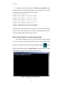
Binary Counter Design Entry: Assembly Language Example
After the FPGA configuration file has been created to allow 8031 operation and LED
access, we are now ready to enter the software portion of the binary counter design. To do this,
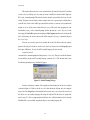
first open up a command window by double clicking on the 8051_c_asm Icon,
from the
Window’s Desktop. This will bring up a Command Window (as shown in Figure 2.4) in which
the Metalink 8051 assembler and/or the SDCC 8051 compiler can be run.
Figure 2.4: Opening up a Command Window
13
Version 1.00
This window allows the user to enter commands directly from the keyboard. The window
is made active by clicking on it once using the mouse. Initially the window should display the
X:\> as the command prompt. This indicates that the student’s network drive has been set as the
default. To begin to enter the binary counter example, first create a separate top-level folder that is
on the X: drive. Such a folder will be present under the student’s account on each system that the
student can access. Set the name of this folder to bcount_s. This can be done by typing the command mkdir bcount_s at the command prompt and then pressing the <enter> key (or it can be
done using the New Folder option after invoking the My Computer window and selecting the X:
drive). Next change the current context to this folder using the cd bcount_s command (and press
the <enter> key).
Now one can create the source-level assembly file or the C file that describes the software
portion of the design. To do this we need to enter a basic text editor such as the Notepad program
that is part of Windows. To create the 8051 assembly language file, first enter the
notepad bcount.a51
command at the command prompt and then press the <enter> key. This gives the file the filename
bcount with the extension 8051 assembly language extension of a51. The first time this is done
the following warning message window will appear.
Figure 2.5: Initial Warning Message
Press the yes button to continue. The notepad text editor should now be the active window
as shown in Figure 2.6. If this is not the case, select this window by clicking on it once using the
mouse. Once the Notepad text editor window has been made active, one can enter the source level
file (in this case an assembly language file) using the keyboard. The file has been assigned the
name bcount.a51. (It is very important the this file have the *.a51 extension since this is how the
Metalink 8051 cross-assembler script knows that it is an assembly language file.
14
Version 1.00
Figure 2.6: Notepad Editing Window
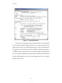
The 8031 source code for the binary counter is shown in Listing 2.2. The comments within
the code describe its operation. It should be noted that the code uses software timing that is based
upon the 8031 system clock rate of 12 MHZ and the number of cycles that each instruction in the
delay loop takes to execute. Since the clock on the actual XS40 V 1.4 platform is programmed to
12.5 MHZ the actual execution will be about 4% faster than that indicated. Students should be
aware of the advantages and disadvantages of using software derived timing. Also students should
note that the LED output latch is accessed in a memory-mapped manner as if it were a standard
RAM type memory location.
15
Version 1.00
; Binary Counter: 8031 Assembly Example
;
Software Implementation -- FPGA acts as simple I/O latches
;
B. Earl Wells, S.M. Loo, July 2002, UAH.
$MOD51
; Symbolic Declarations
STACKTOP
EQU 70H ; start of stack (stack grows up)
LEDREG
EQU 0F000H ; discrete LEDs register address (memory mapped in Xilinx FPGA)
; Program Code Area -- Note: 8031 begins execution after reset at location 0
CSEG
ORG 0000H ; start code at location 0H
; main routine: periodically (about once a second) outputs binary value
; to least significant four segments of the 7 segment LED
START:
MOV SP,#STACKTOP ; initialize stack pointer (to allow sub calls)
MOV A,#0 ; Let 4 least significant bits of register A represent
; the binary counter. (upper 4 bits will be ignored)
; Initialize the counter to 0
MLOOP:
MOV DPTR,#LEDREG
MOVX @DPTR,A
CALL DELAY
INC A
ANL A,#0FH
JMP MLOOP
;
;
;
;
;
;
Set up pointer to memory mapped LED registers
output the four bits to the discrete LEDs
wait about 1 second before continuing
increment counter by 1
Mask out upper 4 bits
continue the process until processor is reset
; this subroutine uses three nested loops to “waste” about 1 second
DELAY:
;
| 2uS (for CALL statement)
PUSH ACC ; Save current context
| 2uS
PUSH B
; (i.e. all regs which are modified)
| 2uS
MOV COUNT,#8 ;
| 2uS
LP1:
MOV B,#0 ;
| 2uS
|
LP2:
MOV A,#0
; 2uS
|
|
DJNZ ACC,$ ; 256x2 = 512 uS | 256 x 516 = | 8x132,100 =
DJNZ B,LP2
; 2uS
| 132,096uS
| 1.0568 S
DJNZ COUNT,LP1 ;
| 2us
|
POP B ;
restore previous
| 2uS
POP ACC ; context
| 2uS
RET ;
| 2uS
; total estimated execution time = 1.056814 S
; Data Segment Area -- Note: in this design the data segment uses the same address
;
space as the code segment. Care should be taken that these do
;
not overlap!
DSEG
ORG 60H
COUNT:
DS 1 ; memory location reserved for the outer loop counter value
END
Listing 2.2: Binary Counter Example: Assembly Language Source Code
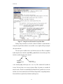
Once the assembly language code has been entered using the text editor then the file
should be saved. This is accomplished using the Save command that is under the File menu of the
Notepad window as shown in Figure 2.7.
16
Version 1.00
Figure 2.7: Saving the Source File from the Notepad Text Editor
Warning: Always remember to save the file each time it is modified. A common mistake is
to forget this step which means that the cross assembler or cross compiler will be processing the
old version of the file!
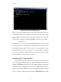
The next step is to assemble the source-level file that was just saved. This is accomplished
by first using the mouse to make the original 8051_c_asm window the active window again. Then
invoke the assembler by typing in the command
asm bcount
Metalink 8051
Assembler Command
Script Name
File name with
out the .a51 extension
at the command prompt and then press the <enter> key. This command will assemble the
bcount.a51 file and if there are no errors (as shown in Figure 2.8) produce an executable file
named bcount.hex. This file is in standard Intel Hex Format which is a portable object code standard that can be directly downloaded to the XS 40 board along with the corresponding hardware
bit stream file that was produced by the hardware synthesis process.
17
Version 1.00
Figure 2.8: An Error Free Assembly Scenario
If there are errors in the assembly language file an error message will be produced in the command window. To determine the statements that are causing the error one must view the assembly
language listing file. This file has the extension *.lst. In this case the file name is bcount.lst. This
can be done using a text editor. To do this with the Notepad text editor just enter the command
notepad bcount.lst
and then press the <enter> key. A new window will appear that shows the object code generated
for each line of source code. Any warning or error messages will be present just above or below
the line that has the incorrect syntax. This file is very wide (i.e. has very long lines), so using a
large window is best. The *.lst file is for viewing only -- do not edit it! It will be overwritten the
next time the cross assembler is executed and all changes to the source code will be lost. Always
edit the assembly source file (the file with the.a51 extension).
Programming (Device Configuration) Phase
Once the Intel Hex record file (in this case the bcount.hex file) is successfully produced it
can be used along with the Xilinx bit map file to configure and program the XS 40 system by
invoking the GXSLOAD program. Before this can be accomplished, though, the programmable
clock oscillator on the newer XS 40 boards needs to be set at 12.5 MHZ. To do this, first remove
the power connector from the XS40 Board, then remove the jumper J12 and reposition it so that it
is in the “set” position, reconnect the power cable and run the GXSSETCLK Program by double
18
Version 1.00
clicking on its icon which is on the windows desktop. This should cause the following dialog box
to appear.
Set Button
Divisor for
12.5 Mhz
Clock
Figure 2.9: Dialog Box for GXSSETCLK Program.
To program the clock for 12.5 Mhz, the closest we can get to the 12 Mhz clock that was present on
the previous generation boards, simply enter the divisor of 8 as shown. Do not check the External
Clock box since we want to use the internal clock. Press the SET button to program the clock.
After the clock is programmed, disconnect the power cable again and reposition the jumper J12 to
its original position, then reconnect the power cable. This procedure only needs to be performed
once for each desired clock speed. The programmable oscillator will remain programmed even
when power is removed to the card.
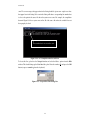
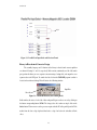
The GXSLOAD utility is used load both the hardware configuration and the executable
program portions of the design. This Windows based software initially configures the FPGA in a
manner to allow it to place 8031 program code that is received over the parallel port directly into
the on-board SRAM. After the FPGA is configured in this manner, the GXSLOAD software then
sends the program code through the parallel port after it performs the necessary conversion from
Intel Hex format. After this is complete, the GXSLOAD software sends the user created bit map
file (created using the Xilinx design tools using schematic elements that support standard 8031
operation) to reconfigure the FPGA to obtain its final configuration. After this operation begins
when the 8031 is reset in the manner specified by the user (in the examples specified in this document, this will occur when the user strobes bit D5 of the parallel port high and then low
using GXSPORT software on the PC).
To configure the XS 40 for 8031 based operation, the following procedures should be performed. First, connect the XS 40 to the AC adapter and make sure the parallel cable is connected
to the power supply side of the XS 40. Connect the other end of the cable to the host PC’s parallel
port. Then from the Windows desktop, click on the GXSLOAD icon to bring up the GXSLOAD
19
Version 1.00
window as shown in Figure 2.15. Then simultaneously select both the Xilinx bit map file which
has the desired FPGA configuration (with the 8031 supporting logic as described in the FPGA
hardware sections of Chapter 1 -- along with any specific hardware needed to implement the I/O
peripherals) and select the 8031 Intel Hex file (bcount.hex in this case) by clicking on both file
icons while pressing the control key on the keyboard. Then simply drag and drop the two files into
the appropriate section of the GXSLOAD window. After this is done, click on the LOAD button
and the device should begin the configuration process which will take several seconds.
Load
Button
Downloadable
file formats
Area to drop
the hardware
(*.bit) file
Area to drop
the software
(*.hex) file
Figure 2.10: The Downloading Program, GXSLOAD.
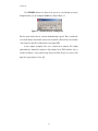
Before execution can begin, the 8031 processor may need to be reset (although this sometime occurs automatically due to switching transients in the XS 40 board). As mentioned previously, this can be done by strobing the parallel port bit D5 from the low to logic high and then
back to logic low using the GXSPORT program in the manner that is suggested in this document.To control these bits click on the GXSPORT program icon that is located on the windows
desktop. This will activate the following window.
The reset
Bit
strobe
button
Figure 2.11: Resetting the 8031 with using GXSPORT
Getting the final version of software/FPGA hardware often requires many iterations. Using
the Load button on the GXSLOAD with the same files selected will accomplish this without the
need to drag and drop the new versions of the files into the GXSLOAD window.
20
Version 1.00
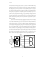
After the XS 40 is configured and the 8031 reset, four of the seven segments of the LED
should act as a binary counter with segment a being the least significant bit and segment d being
the most significant bit.
Least Significant Bit
a
b
c
d
Most Significant Bit
Figure 2.12: Active LED Segments.
Binary Counter Design Entry: C Programming Language Example
Often we would prefer to represent software designs using a high-level language such as
C. Fortunately this can be accomplished using the SDCC C Cross-compiler in much the same way
as the assembly language version was created using the MetaLink assembler. To do this, first open
up a command window by double clicking on the 8051_c_asm Icon,
from the Window’s
Desktop. This will bring up a Command Window in which the SDCC 8051 C cross compiler can
be run. Initially the window should display the X:\> as the command prompt which indicates that
the student’s network drive has been set as the default. To begin to enter the binary counter example, first create a separate top-level folder that is on the X: drive. Such a folder will be present
under the student’s account on each system that the student can access. Set the name of this folder
to bcount_s. If the folder is not already present, this can be done by typing the command
mkdir bcount_s
at the command prompt and then pressing the <enter> key otherwise, skip this step. After the
folder is created, change the current context to this folder using the cd bcount_s command (and
press the <enter> key).
Now one can create the source-level C file that describes the software portion of the
design. To do this using the Notepad text editor type the
notepad bcount.c
command at the command prompt and then press the <enter> key. This gives the file the filename
bcount with the extension of .c. The first time this is done the a warning message window will
appear. If this occurs, press the yes button to continue. The Notepad text editor should now be the
active window. If this is not the case, select this window by clicking on it once using the mouse.
21
Version 1.00
Once the Notepad text editor window has been made active, one can enter the source level file (in
this case a C language file) using the keyboard. The file has been assigned the name bcount.c. (It is
very important the this file have the *.c extension since this is how the SDCC cross-compiler script
knows that it is a C language source file.
The C version of the same binary counter program as was presented in the previous section is
shown in Listing 2.3. The file has the same general structure as the assembly language version with a
pointer being used to access the memory-mapped LED output. This pointer was declared using the
SDCC special xdata storage specifier. This specifier is 8031 specific and allows the pointer to point
to external RAM. Unlike the assembly language version, the software timing was computed experimentally instead of computing the number of instruction cycles. The main delay loop would be sensitive not only to the clock frequency of the 8031 but also to the compiler optimization techniques that
are employed. A more complete description of this code is contained in its comments.
/* Binary Counter: -- C Programming Language Example
/* Software Implementation -- FPGA acts as a simple output latch
/*
B. Earl Wells, S.M. Loo, August 2002, UAH. */
*/
*/
/* Delay routine -- experimentally set to create a delay of about */
/*
one second.
*/
void delay(void)
{
unsigned int i,j;
for (i=0;i<2;i++) {
/* nested FOR loops to “waste” time */
for (j=0;j<57613;j++);
}
}
/* main routine: periodically (about once a second) outputs binary value */
/* to discrete LEDS */
void main (void)
{
/* pointer declaration -- set to point to address of LED latch */
xdata unsigned char * led = (xdata unsigned char *) 0xf000;
unsigned char count; /* current count value */
count = 0; /* initialize count value to zero */
/* infinite loop
while (1) {
count &= 0x0f;
*led = count;
delay();
/*
count++;
/*
}
*/
/* Mask out upper 4 bits */
/* output counter value */
wait about 1 second before continuing */
increment count value by one */
}
Listing 2.3: Binary Counter Example: C Language Source Code
22
Version 1.00
Once the C source code has been entered using the text editor then the file should be saved.
This is accomplished using the Save command that is under the File menu of the Notepad window.
Warning: Always remember to save the file each time it is modified. A common mistake is
to forget this step which means that the SDCC C cross compiler will be processing the old version
of the file!
The next step is to compile the source-level C file that was just saved. This is accomplished
by first using the mouse to make the original 8051_c_asm window the active window again. Then
invoke the SDCC C cross compiler by typing in the command
cc bcount
SDCC C Cross
Compiler Command
Script Name
File name with
out the .c extension
at the command prompt and then press the <enter> key. This command will compile the bcount.c
file and if there are no errors (as shown in Figure 2.13) produce an executable file named
bcount.hex. This file is in standard Intel Hex Format which is a portable object code standard that
can be directly downloaded to the XS 40 board along with the corresponding hardware bit stream
file that was produced by the hardware synthesis process.
Figure 2.13: An Error Free C Compilation
If there are errors in the C source file, one or more error messages will be displayed in the command window as shown in Figure 2.11. If there are many errors one may have to use the left scroll
bar to view all of them. In general, there may be many error messages generated for each real
23
Version 1.00
error. The error messages that appear first in the listing should be given more weight over those
that appear later in the listing. Each error in the listing will show a corresponding line number that
is close to the point in the source file where the syntax error occurs. For example, the compilation
shown in Figure 2.14 has a syntax error on line 10 of the source file where the variable k has not
been properly declared
Line
L number that is at or near the error
Figure 2.14: A C Compilation that has an Error
To locate this line, go back to the Notepad window and select the Goto... option from the Edit
window. This should bring up the Goto line dialog box. Enter the number 10 and press the OK
button (or press <control> g from the keyboard).
Figure 2.15: Notepad Goto Line Dialog Box
24
Version 1.00
The cursor should move to line 10 where the error can be found as shown in Figure 2.16.
Line 10
Error (should be an i here)
Figure 2.16: Locating the Error in the C Source Code
After finding and fixing the errors in the file, first save the new version of the file to disk using the
Save option from the File menu. Then recompile the file in the manner discussed previously.
Once the Intel Hex record file (in this case the bcount.hex file) is successfully produced it
can be used along with the Xilinx bit map file to configure and program the XS 40 system by
invoking the GXSLOAD program. This Windows based software initially configures the FPGA
in a manner to allow it to place 8031 program code that is received over the parallel port directly
into the on-board SRAM. After the FPGA is configured in this manner, the GXSLOAD software
then sends the program code through the parallel port after it performs the necessary conversion
from Intel Hex format. After this is complete, the GXSLOAD software sends the user created bit
The rest of the process is just like it was for the assembly language version. The resulting
Intel hex record output file can then be loaded onto the XS 40 along with the Xilinx bit-map file
using the GXSLOAD utility and the GXSPORT utility can be used to reset the 8031 processor.
25
Version 1.00
Chapter 3: Software Implementations of a Binary to Hex Converter
Example
In this chapter, a binary to seven segment display converter example will be used to illustrate how simple I/O devices can be created in the reconfigurable FPGA hardware and driven by
microcontroller software. The design will drive an external seven-segment common cathode LED
that is to be connected to pins 8, 9, 6, and 77 of XS 40 (which comes directly from the Xilinx
XC4010XL FPGA) as shown in Figure 1.1. In a similar manner, the inputs to this design will be
driven directly by the least significant four bits of the parallel port switches on the XS 40 (labeled
for historic reasons DIP 1 -- DIP4).
Background
A single seven-segment indicator can be used to display the digits ‘0’ through ‘9’ and the
hexadecimal symbols ‘A’ through ‘F’ (with symbols ‘b’, and ‘d’ being displayed in lower case) by
lighting up the appropriate set of segments. For example, the number ‘8’ can be displayed by illuminating all seven segments and the lower case letter ‘b’ can be displayed by illuminating the segments labeled c,d,e,f, and g for the seven segment display element that is shown in Figure 3.1.:
7 Seg LED
R a
a
f
b
g
e
Logic High
Lights
Segments
R b
cp
c
d
R g
Common Cathode
Figure 3.1: Seven Segment Display Unit
One common type of seven segment display unit utilizes Light Emitting Diodes, LEDs, as
the display elements. In this arrangement, each segment that makes up the seven segment display
unit is a separate light emitting diode (LED) that will light up when it is forward biased. Often
commercially available seven-segment LED display units minimize the number of external pins
26
Version 1.00
needed by internally connecting together one node of each of the seven individual LEDs. In one
arrangement, the common cathode, the cathodes of the diodes have a common connection point. If
this common point is connected to ground and a set of current limiting resistors are connected in
series with the individual segments then each segment of the display can be independently illuminated by placing a logic high on the corresponding segment lead (assuming the logic device is
capable of sourcing enough current). The binary to seven segment display example assumes that
an external common cathode seven segment LED will be used as the targeted display element
with the common cathode point being connected to ground. Thus a logic high will be required to
light up each segment.
Figure 3.2 shows a block diagram of the configuration of the display converter system that
is to be designed and implemented on the XS 40. The FPGA will be configured to support 8031
control and memory interfaces. It will also be configured to support a four-bit input port and a
seven bit output port. The input port will connect to the four dip switches and the output port will
drive the seven segment display. The 8031 will be programmed to poll the parallel port input
switches and drive the seven segment display in a manner in which the hexadecimal symbol associated with the four bit input is displayed. Thus the symbol 0 would be displayed if all of the input
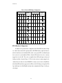
bits were logic low, and the symbol 8 would be displayed if bit I<3> was high and the rest low.
Table 3.1 shows the desired display configuration for each of the 16 possible input scenarios.
outputs
to LED
O<1>
MSB
LSB
80C31
SRAM
bintohex
software
Output Port
I<3>
I<2>
I<1>
I<0>
Input Port
inputs
from
external
DIP
switches
12.5 MHZ
CLK
a
O<0>
O<5>
f
b
g
O<6>
O<4>
e
O<3>
O<2>
c
d
Figure 3.2: Display Converter Seven Segment Display System Overview
27
Version 1.00
Table 3.1: Desired LED Display Configurations
Inputs
Inputs
Display
I3
I2
I1
I0
0
0
0
0
0
0
Configuration
Display
I3
I2
I1
I0
0
1
0
0
0
0
1
1
0
0
1
0
1
0
1
0
1
0
0
0
1
1
1
0
1
1
0
1
0
0
1
1
0
0
0
1
0
1
1
1
0
1
0
1
1
0
1
1
1
0
0
1
1
1
1
1
1
1
Configuration
FPGA Hardware Configuration
In addition to the general hardware configuration of the Xilinx FPGA described in Chapters 1 which allows normal 8031 operation with the 32K SRAM and the output latch interface
which is shared between the individual LEDs and the seven segment LED, an additional input
device needs to be created within the FPGA to allow the DIP switches to be read as a memory
mapped device by the 8031. This can be accomplished by the DIP switch input selection and
latching circuit that is shown in Figure 3.3. This selection circuitry is memory-mapped to the
combined data/code address location of D000H. The circuitry is used to drive the AD_SEL line
which allows DIP switch data to appear on the A/D lines of the 8031 during a read operation. This
logic should replace the AD_SEL pull down logic that was implemented in Figure 2.3 of the previous chapter.
28
Version 1.00
A_IN15
A_IN14
A_IN13
AD_SEL
A_IN12
IN_OE_
Figure 3.3: Parallel Port Input Latch and Selection Circuit
Binary to Hexadecimal Converter Design
The assembly language and C solutions to the binary to hexadecimal converter problem
are shown in Listings 3.1 and 3.2, respectively. Both versions continuously read the 4 bit switch
port, perform the binary to seven segment conversion using a lookup table, and output the seven
segment value to the LED port. To control these bits click on the GXSPORT program icon that is
located on the windows desktop. This will activate the following window.
Input Bits
Reset bit
Figure 3.4: GXSPORT Window, (non counting mode)
In this window, the states of each of the 8 bits on the parallel port can be set or reset by clicking on
the button corresponding button, D7-D0. The changes take effect when one single clicks on the
Strobe button. This means to reset the processor requires that bit D5 of the parallel port bit D5 be
strobed from the low to logic high and then back to a logic low before the other bits will take
effect.
29
Version 1.00
The GXSPORT window also allows for the port to be cycled through successively
through the binary cycle by checking the Count box as shown in Figure 3.5.
Figure 3.5: GXSPORT Window, (counting mode)
Here the count is advanced by one, each time the Strobe button is pressed. This is a useful mode
to test out the binary to hexadecimal converter, since the bits D3 to D0 can all be cleared and then
easily advanced to show all 16 symbols on the seven segment LED.
A more complete description of the code is contained in its comments. The resulting
implementation is functionally equivalent to that performed in the FPGA hardware alone as
described in Chapter 3 of the manual Getting Started with Xilinx Design Tools and the XS40
Rapid Prototyping Platform, Version 2[2].
30
Version 1.00
; Binary to Hexadecimal Converter: 8031 Assembly Example
;
Software Implementation -- FPGA acts as simple I/O latch
;
B. Earl Wells, S.M. Loo, August 2002, UAH.
$MOD51
; Symbolic Declarations
STACKTOP EQU 70H ; start of stack (grows up)
LEDREG
EQU 0F000H ; LED register Address
DIPSW
EQU 0D000H ; Dip Switch Latch Address
; Program Code Area -- Note: 8031 begins execution after reset at location 0
CSEG
ORG 0000H ; start code at location 0H
START:
MOV SP,#STACKTOP ; initialize stack pointer (to allow sub calls)
;
Main Routine : continuously reads the DIP switches and outputs their
;
hexadecimal value on the seven segment LED
MLOOP:
MOV DPTR,#DIPSW ; Set up pointer to memory mapped DIP Switch location
MOVX A,@DPTR
; Place dip switch value in Reg A
CALL BINTOHEX
; Routine to display in hexadecimal the 4 least significant
; bits that are present in the accumulator
JMP MLOOP
; continue the process until processor is reset.
; this subroutine displays on the seven segment LED the hexadecimal
; symbol that corresponds the least significant four bit value
; that is in the accumulator
BINTOHEX:
;
PUSH ACC ; Save current context (i.e. all registers that will be modified)
ANL A,#0FH
; clear upper 4 bits of A
; (allows these bits to be ignored don’t cares)
MOV DPTR,#LEDTABLE ; set DPTR to start of lookup table
MOVC A,@A+DPTR
; input bin pattern associated with the binary value
; that was loaded in the A register
MOV DPTR,#LEDREG
;set DPTR to point to memory mapped seven segment LED Regs
MOVX @DPTR,A
; output the hexadecimal symbols to the seven segment LED
POP ACC
RET
; hexadecimal lookup table
LEDTABLE: DB 03FH,006H,05BH,04FH,066H,06DH,07DH,007H
DB 07FH,067H,077H,07CH,039H,05EH,079H,071H
; Data Segment Area -- Note: in this design the data segment uses the same address
;
space as the code segment. Care should be taken that these do not
;
overlap!
DSEG
ORG 60H
COUNT:
DS 1 ; memory location reserved for the outer loop counter value
END
Listing 3.1: Binary to Hexadecimal Converter: Assembly Language Source Code
31
Version 1.00
/* Binary to Hexadecimal Converter: C Programming Language Example */
/* Software Implementation -- FPGA acts as simple I/O latches
*/
/*
B. Earl Wells, S.M. Loo, August 2002, UAH.
*/
/* Address of seven segment LED latch */
xdata unsigned char * sevsegled = (xdata unsigned char *) 0xf000;
/* Parallel Port Input Switch Address */
xdata unsigned char * dipswitch = (xdata unsigned char *) 0xd000;
/* seven segment hexadecimal lookup table */
const unsigned char ledtable[16] = {0x3f, 0x06,0x5b,0x4f,0x66,0x6d,0x7d,0x07,
0x7f,0x67,0x77,0x7c,0x39,0x5e,0x79,0x71};
/* Function to display on the seven segment LED the hexadecimal symbol
/* that which corresponds to the least significant four bit value of
/* the input argument
void bintohex(unsigned char bvalue)
{
bvalue &= 0x0f;
/* mask out upper four bits */
*sevsegled = ledtable[bvalue];/* output appropriate bit pattern from
}
*/
*/
*/
lookup table */
/* Main Routine : continuously reads the Input switches and outputs their
/*
hexadecimal representation on the seven segment LED
void main (void)
{
*/
*/
unsigned char binvalue; /* current count value */
while (1) {
binvalue = *dipswitch;
bintohex(binvalue);
}
/* read DIP switch value */
/* display value on 7 seg. LED */
}
Listing 3.2: Binary to Hexadecimal Converter: C Language Source Code
32
Version 1.00
Chapter 4: Software Implementations of a Hexadecimal Counter
In this chapter, the two previous design examples from Chapter 2 (the binary counter) and
Chapter 3 (the binary to seven segment hexadecimal converter) have been combined in a modular
fashion into a single program to implement a complete hexadecimal counter. The final program
results in successive hexadecimal symbols being displayed at a rate of approximately 1HZ on the
XS 40 seven segment LED. Figure 4.1 shows a block diagram of the hardware aspects of the
hexadecimal counter. The FPGA must be configured to support 8031 control and memory interfaces. It also must be configured to support the seven bit output port which drives the seven segment display. The 8031 should be programmed to repetitively count in binary, convert the binary
value to seven segment hexadecimal format, and to drive the seven segment display in a manner in
which the hexadecimal symbol associated with the binary count value is displayed.
outputs
to LED
O<1>
12.5MHZ
CLK
SRAM
bintohex
software
Output Port
80C31
a
O<0>
O<5>
f
b
g
O<6>
O<4>
e
O<3>
O<2>
c
d
Figure 4.1: Hexadecimal Counter Hardware Setup
Hardware Configuration
No additional hardware is needed to be implemented inside the FPGA. Either of the FPGA
configurations described in Chapter 2 or 3 can be used to implement the combined design.
Hexadecimal Counter Design
The assembly language and C solutions to the binary to hexadecimal converter problem
are shown in Listings 4.1 and 4.2, respectively. Both versions are simply modular combinations of
the two previous programs. A more complete description of the code is contained in its comments. The resulting implementation is functionally equivalent to that performed in FPGA hardware alone as described in Chapter 4 of the manual Getting Started with Xilinx Design Tools and
the XS40 Rapid Prototyping Platform [2].
33
Version 1.00
; Hexadecimal Counter: 8031 Assembly Example
;
Software Implementation -- FPGA acts as a simple latch
;
B. Earl Wells, S.M. Loo, August 2002, UAH.
$MOD51
; Symbolic Declarations
STACKTOP EQU 70H ; start of stack (grows up)
LEDREG
EQU 0F000H ; LED register Address
; Program Code Area -- Note: 8031 begins execution after reset at location 0
CSEG
ORG 0000H ; start code at location 0H
; main routine: periodically (about once a second) displays the hexadecimal value of
;
the current count value, then increments the count by one
START:
MOV SP,#STACKTOP ; initialize stack pointer (to allow subroutine calls)
MOV A,#00H
; initialize counter to 0
MLOOP:
CALL BINTOHEX
; Routine to display in hexadecimal the 4 least significant
; bits that are present in the accumulator
INC A
; Increment count value by one
CALL DELAY
; wait about 1 second
JMP MLOOP
; continue the process until processor is reset.
; this subroutine displays on the seven segment LED the hexadecimal
; symbol which corresponds the least significant four bit value
; that is in the accumulator
BINTOHEX:
PUSH ACC ; Save current context (i.e. all registers that will be modified)
ANL A,#0FH
; clear upper 4 bits of A
; (allows these bits to be ignored don’t cares)
MOV DPTR,#LEDTABLE ; set DPTR to start of lookup table
MOVC A,@A+DPTR
; input bin pattern associated with the binary value
; that was loaded in the A register
MOV DPTR,#LEDREG
; set DPTR to point to memory-mapped 7 segment LED Regs
MOVX @DPTR,A
; output the hexadecimal symbols to the seven segment LED
POP ACC
RET
; hexadecimal lookup table
LEDTABLE:
DB 03FH,006H,05BH,04FH,066H,06DH,07DH,007H
DB 07FH,067H,077H,07CH,039H,05EH,079H,071H
; Data Segment Area -- Note: in this design the data segment uses the same address
;
space as the code segment. Care should be taken that these do
;
not overlap!
; this subroutine uses three nested loops to waste about 1 second
DELAY:
;
| 2uS (for CALL statement)
PUSH ACC ; Save current context
| 2uS
PUSH B
; (i.e. all regs which are modified)
| 2uS
MOV COUNT,#8 ;
| 2uS
LP1:
MOV B,#0 ;
| 2uS
|
LP2:
MOV A,#0
; 2uS
|
|
DJNZ ACC,$ ; 256x2 = 512 uS | 256 x 516 = | 8x132,100 =
DJNZ B,LP2 ; 2uS
| 132,096uS
| 1.0568 S
DJNZ COUNT,LP1 ;
| 2us
|
POP B ;
restore previous
| 2uS
POP ACC ; context
| 2uS
RET ;
| 2uS
; total estimated execution time = 1.056814 S
; Data Segment Area -- Note: in this design the data segment uses the same address
;
space as the code segment. Care should be taken that these do
;
not overlap!
DSEG
ORG 60H
COUNT:
DS 1 ; memory location reserved for the outer loop counter value
END
Listing 4.1: Hexadecimal Counter: Assembly Language Source Code
34
Version 1.00
/* Hexadecimal Counter: C Programming Language Example
/* Software Implementation -- FPGA acts as a simple latch
/*
B. Earl Wells, S.M. Loo, August 2002, UAH.
*/
*/
*/
/* Address of seven segment LED latch */
xdata unsigned char * sevsegled = (xdata unsigned char *) 0xf000;
/* Delay routine -- experimentally set to create a delay of about */
/*
one second.
*/
void delay(void)
{
unsigned int i,j;
for (i=0;i<2;i++) {
for (j=0;j<57613;j++); /* nested FOR loop to waste time */
}
}
/* seven segment hexadecimal lookup table */
const unsigned char ledtable[16] = {0x3f, 0x06,0x5b,0x4f,0x66,0x6d,0x7d,0x07,
0x7f,0x67,0x77,0x7c,0x39,0x5e,0x79,0x71};
/* Function to display on the seven segment LED the hexadecimal symbol which */
/* corresponds the least significant 4 bit value of the input argument
*/
void bintohex(unsigned char bvalue)
{
bvalue &= 0x0f;
/* mask out upper four bits */
*sevsegled = ledtable[bvalue];/* output appropriate bit pattern from lookup table */
}
/* main routine: periodically (about once a second) displays the hex value of
/*
the current count value, then increments the count by one
void main (void)
{
unsigned char count; /* current count value */
count = 0; /* initialize count value to 0 */
while (1) {
bintohex(count); /* output current count value */
delay();
/* wait about one second */
count ++;
/* increment count by one */
}
}
Listing 4.2: Hexadecimal Counter: C Language Source Code
35
*/
*/
Version 1.00
Chapter 5: Hybrid Implementations of a Hexadecimal Counter
In this chapter, hybrid hardware/software solutions to the hexadecimal counter are introduced. These solutions all have one major component that is present in the FPGA while the other
major component of the design is present in the 8031 software. Design examples include the cases
where the binary to hexadecimal conversion is performed in the FPGA hardware and the binary
counter is implemented in the 8031 software and the cases where the binary to hexadecimal conversion is performed in 8031 software and the binary counter is implemented inside the FPGA
(both polled and interrupt driven solutions to the second scenario are presented). In all design
examples both assembly language and C programming language solutions are shown.
Case I: Binary to Hexadecimal Conversion in FPGA Hardware
FPGA Hardware Configuration
For this example, the following logic replaces the seven segment latch presented in
Figure 2.2. This logic contains traditional schematic elements as well as a hardware description
macro. The circuitry acts as a smart memory-mapped latch that accepts a four-bit binary value and
outputs to a seven segment LED the corresponding hexadecimal symbol. This latch is memory
mapped to location B000H.
AD_IN0
AD_IN1
AD_IN2
A_IN15
AD_IN3
A_IN14
A_IN13
WR_IN_
LEDBUF7
A_IN12
Figure 5.1: Hexadecimal Counter -- Hybrid Example:
(Hardware Implementation of Binary to Hexadecimal Converter Circuit)
Listing 5.1 shows the VHDL model which is associated with the FPGA based binary to
hex conversion macro which is present in the design.
36
Version 1.00
-- VHDL Template File for binary to hex converter example
-- File: bintohex.vhd
-- B. Earl Wells, May 2000, University of Alabama in Huntsville
library IEEE;
use IEEE.std_logic_1164.all;
entity bintohex is
port (
I: in STD_LOGIC_VECTOR (3 downto 0);
O: out STD_LOGIC_VECTOR (6 downto 0)
);
end bintohex;
architecture bintohex_arch of bintohex is
begin
-- with/select construct
-- used to create a simple 7 output/ 4 input truth table (with inputs
-- on the right side as shown below).
with I select
-outputs
inputs
-O<6> O<5> O<4> O<3> O<2> O<1> O<0>
I<3> I<2> I<1> I<0>
-gfedcba
O <=
“0111111”
“0000110”
“1011011”
“1001111”
“1100110”
“1101101”
“1111101”
“0000111”
“1111111”
“1100111”
“1110111”
“1111100”
“0111001”
“1011110”
“1111001”
“1110001”
“-------”
when
when
when
when
when
when
when
when
when
when
when
when
when
when
when
when
when
“0000”,
“0001”,
“0010”,
“0011”,
“0100”,
“0101”,
“0110”,
“0111”,
“1000”,
“1001”,
“1010”,
“1011”,
“1100”,
“1101”,
“1110”,
“1111”,
others;
end bintohex_arch;
Listing 5.1: Binary to Hexadecimal Counter: VHDL Source Model
Software Configuration
Both assembly language and C versions of the code treat the new hardware as a memorymapped device. The programs perform the binary counting operation and then output the raw
binary value to the memory-mapped latch. The difference between this and previous implementations is that the FPGA based peripheral device is smart, in the sense that it stores the four bit value
in memory and performs the necessary seven segment conversions in hardware. A more complete
description of the code is contained in its comments.
37
Version 1.00
; Hexadecimal Counter: 8031 Assembly Example
; Hybrid Implementation -- Binary Counter in Software,
;
Binary to hexadecimal Conversion in FPGA
;
B. Earl Wells, S.M. Loo, August 2002, UAH.
$MOD51
; Symbolic Declarations
STACKTOP
EQU 70H ; start of stack (grows up)
LEDBINRG
EQU 0B000H ; 4 bit binary register that latches the data
; which feeds into binary to hexadecimal converter
; circuit that is implemented inside the FPGA HW
; Program Code Area -- Note: 8031 begins execution after reset
CSEG
ORG 0000H ; start code at location 0H
; main routine: periodically (about once a second) sends a new
;
to the binary to hexadecimal converter circuit
;
within the external FPGA
START:
MOV SP,#STACKTOP ; initialize stack pointer (to allow
;
Main Routine:
MOV A,#00H
; initialize counter to 0
at location 0
count value
that is located
subroutine calls)
MLOOP:
MOV DPTR,#LEDBINRG ; Output Data to HW latch that feeds the binary to
MOVX @DPTR,A
; hexadecimal converter that is implemented inside the
; Xilinx FPGA
INC A
; increment count value by one
CALL DELAY
; wait about 1 second
JMP MLOOP
; continue the process until processor is reset.
; this subroutine uses three nested loops to waste about 1 second
DELAY:
;
| 2uS (for CALL statement)
PUSH ACC ; Save current context
| 2uS
PUSH B
; (i.e. all regs which are modified)
| 2uS
MOV COUNT,#8 ;
| 2uS
LP1:
MOV B,#0 ;
| 2uS
|
LP2:
MOV A,#0
; 2uS
|
|
DJNZ ACC,$ ; 256x2 = 512 uS | 256 x 516 = | 8x132,100 =
DJNZ B,LP2 ; 2uS
| 132,096uS
| 1.0568 S
DJNZ COUNT,LP1 ;
| 2us
|
POP B ;
restore previous
| 2uS
POP ACC ; context
| 2uS
RET ;
| 2uS
; total estimated execution time = 1.056814 S
; Data Segment Area -;
;
DSEG
ORG 60H
COUNT:
DS 1 ; memory
END
Note: in this design the data segment uses the same address
space as the code segment. Care should be taken that these
do not overlap!
location reserved for the outer loop counter value
Listing 5.2: Hexadecimal Counter -- Hybrid Example: Assembly Language Source Code
(Binary Counter in Software -- Binary to Hexadecimal Converter in FPGA)
38
Version 1.00
/* Hexadecimal Counter: C Programming Language Example
*/
/* Hybrid Implementation -- Binary Counter in Software,
*/
/*
Binary to hexadecimal conversion in FPGA */
/*
B. Earl Wells, S.M. Loo, August 2002, UAH.
*/
/* 4 bit binary register that latches the data which feeds into binary to */
/* hexadecimal converter circuit that is implemented inside the
*/
/* Xilinx FPGA Hardware
*/
xdata unsigned char * ledbinrg = (xdata unsigned char *) 0xb000;
/* Delay routine -- experimentally set to create a delay of about */
/*
one second.
*/
void delay(void)
{
unsigned int i,j;
for (i=0;i<2;i++) {
for (j=0;j<57613;j++);
/* nested FOR loops to “waste” time */
}
}
/* main routine: periodically (about once a second) sends a new count value
*/
/*
to the binary to hexadecimal converter circuit that is located */
/*
within the external FPGA
*/
void main (void)
{
unsigned char count; /* current count value */
count = 0;
/* initialize count value to 0 */
while (1) {
*ledbinrg = count; /* output count value directly to hexadecimal converter */
/* which is implemented inside the FPGA
*/
delay();
/* wait */
count ++;
/* increment the count value by one */
}
}
Listing 5.3: Hexadecimal Counter -- Hybrid Example: C Language Source Code
(Hexadecimal Counter in software -- Binary to Hexadecimal Converter in FPGA)
Case II: Binary Counter in FPGA Hardware
FPGA Hardware Configuration
Figure 5.2 shows the additional logic necessary to create a new memory mapped input
device that will implement a binary counter from within the FPGA. In addition to being read as a
memory mapped input at address 9000H this counter has the capability to generate periodic interrupts to the 8031. This replaces the 4 bit input switch circuitry of Figure 3.2. The design also
39
Version 1.00
requires that the simple seven segment latch of Figure 2.2 be restored and that the binary to hexadecimal logic described in Figure 5.1 be removed.
A_IN15
A_IN14
A_IN13
AD_SEL
A_IN12
IN_OE_
AD_OUT0
AD_OUT1
AD_OUT2
AD_OUT3
Figure 5.2: Hexadecimal Counter -- Hybrid Example:
(Hardware Implementation of Binary Counter with 8031 Interrupt Generation Capability)
This circuit requires that one addition be made to the Xilinx User Constraints File to lock
the FPGA INT0 pin to the location which will generate an interrupt to the INT0 pin of the 8031.
40
Version 1.00
To accomplish this on the UAH prototype by placing an external connection between pins 68 and
12 of the XS 40.
# INTERRUPT GENERATING SIGNAL
NET INT0 LOC=P68;
Listing 5.1: Additional Entry to the User Constraints File
The assembly language and C solutions to this hybrid hexadecimal counter problem are
shown in Listings 5.3-5.6. There are two versions of the software, polled and interrupt driven. The
polled versions (Listings 5.3 and 5.4) constantly read the memory-mapped binary counter, perform the binary to hex conversion in software, and then output the seven segment value through
the memory mapped LED port. The interrupt based versions (Listings 5.5 and 5.6) rely upon the
INT0 signal from the FPGA to periodically interrupt the 8031. This requires that the 8031 contain
code which enables the interrupt response, and that there exist an interrupt service routine that
reads once from the memory mapped binary port, performs the binary to hex conversion, and then
writes the seven segment display information to the LED port. It should be noted in the C listing
(Listing 5.5) that in-line assembly is used to set up the interrupt service capabilities of the 8031.
Also the special interrupt function qualifier, interrupt 0 using is used to identify to the compiler
which function will act as the interrupt service routine for interrupt number 0.
41
Version 1.00
; Hexadecimal Counter: 8031 Assembly Example
;
Hybrid Implementation
;
Polled Version -- Binary Counter in FPGA
;
Binary to Hexadecimal Conversion in Software
;
B. Earl Wells, S.M. Loo, August 2002, UAH.
$MOD51
; Symbolic Declarations
STACKTOP EQU 70H ; start of stack (grows up)
LEDREG
EQU 0F000H ; LED register Address
BINCNT
EQU 09000H ; 4 bit Binary Counter Address
; Program Code Area -- Note: 8031 begins execution after reset at location 0
CSEG
ORG 0000H ; start code at location 0H
START:
MOV SP,#STACKTOP ; initialize stack pointer (to allow sub calls)
; main routine: to constantly read binary counter value from FPGA, perform the binary
;
to seven segment conversion in software and output the results to the
;
seven segment LED
MLOOP:
MOV DPTR,#BINCNT ; set DPTR to point to 4 bit binary counter
MOVX A,@DPTR
; Place Count Value in A reg
CALL BINTOHEX
; Call routine to display in hex the 4 least
; significant bits that are in the accumulator
JMP MLOOP
; continue the process until processor is reset.
; This subroutine displays on the seven segment LED the hexadecimal
; symbol which corresponds the least significant four bit value
; that is in the accumulator
BINTOHEX:
PUSH ACC ;Save current context (i.e.all regs that will be modified)
ANL A,#0FH
; clear upper 4 bits of A -- (allows these
; bits to be ignored -- don’t cares)
MOV DPTR,#LEDTABLE ; set DPTR to start of lookup table
MOVC A,@A+DPTR
; input bin pattern associated with binary value
; that was loaded in the A register
MOV DPTR,#LEDREG ; set DPTR to point to seven segment LED Regs
MOVX @DPTR,A
; output the hexadecimal symbols to the 7-seg LED
POP ACC
RET
;
binary to seven segment lookup table
LEDTABLE: DB 03FH,006H,05BH,04FH,066H,06DH,07DH,007H
DB 07FH,067H,077H,07CH,039H,05EH,079H,071H
END
Listing 5.4: Hexadecimal Counter -- Hybrid Example: Assembly Language Source Code
(Polled Version: Binary Counter in FPGA -- Binary to Hexadecimal Converter in software)
42
Version 1.00
/* Hexadecimal Counter: 8031 C Programming Language
/*
Hybrid Implementation -- binary counter in FPGA
/*
Binary to hexadecimal conversion in software
/*
Polled Example
/*
B. Earl Wells, S.M. Loo, August 2002, UAH.
*/
*/
*/
*/
*/
/* External Data pointers */
xdata unsigned char * sevsegled = (xdata unsigned char *) 0xf000;/* seven seg LED */
xdata unsigned char * bincnt = (xdata unsigned char *) 0x9000;
/* binary counter */
/* Lookup table for seven segment LED */
const unsigned char ledtable[16] = {0x3f, 0x06,0x5b,0x4f,0x66,0x6d,0x7d,0x07,
0x7f,0x67,0x77,0x7c,0x39,0x5e,0x79,0x71};
/* Function to display on the 7 segment LED the hexadecimal symbol which corresponds */
/* the least significant 4 bit value of the input argument
*/
void bintohex(unsigned char bvalue)
{
bvalue &= 0x0f;
/* mask out upper four bits */
*sevsegled = ledtable[bvalue]; /* output bit pattern from lookup table */
}
/* main routine: to constantly read binary counter value from FPGA, perform the */
/*
binary to seven segment conversion in software and output the */
/*
results to the seven segment LED
*/
void main (void)
{
unsigned char count; /* current count value */
while (1) {
count = *bincnt; /* read binary counter */
bintohex(count); /* output hexadecimal value */
}
}
Listing 5.5: Hexadecimal Counter -- Hybrid Example: C Language Source Code
(Polled Version: Binary Counter in FPGA -- Binary to Hexadecimal Converter in software)
43
Version 1.00
; Hexadecimal Counter: 8031 Assembly Example
;
Hybrid Implementation: Interrupt Version-- Binary Counter in FPGA
;
Binary to Hexadecimal Conversion in software
;
B. Earl Wells, S.M. Loo, August 2002, UAH.
$MOD51
; Symbolic Declarations
STACKTOP EQU 70H ; start of stack (grows up)
LEDREG
EQU 0F000H ; LED register Address
BINCNT
EQU 09000H ; 4 bit Binary Counter Address
; Program Code Area -- Note: 8031 begins execution after reset at location 0
CSEG
ORG 0000H ; start code at location 0H
JMP STARTUP ; Jump over Interrupt Service Routine Code
; Interrupt Service Routine: writes to the 7-segment display once at each tick of the
;
clock each time returning control to interrupted program.
ORG 0003H ; Start Location for 8031 ISR Routine
ITRPT0: MOV DPTR,#BINCNT ; set DPTR to point to memory mapped 4 bit bin counter
MOVX A,@DPTR
; Place Count Value in A reg
CALL BINTOHEX
; Call routine to display in hex the 4 least significant
; bits that are present in the accumulator
RETI
; return from interrupt
; This is the general start up code for the interrupt service routine. It configures
; the internal register set in a manner which will allow the 8031 to respond to an edge
; triggered interrupt that occurs on the INT0_ pin (port 3, pin 2). This pin will be
; driven by the 4 bit binary counter clocking signal. The actual work of inputting the
; 4-bit value from the external counter is done by the interrupt service routine for
; each tick of the clock. This leaves a lot of time for the 8031 to do useful work. In
; this example, though, the 8031 is normally in an infinite loop after the setup
; operation is complete.
STARTUP:
MOV SP,#STACKTOP;initialize stack pointer (to allow interrupt& sub calls)
MOV TCON,#001H
; set INT0 to be edge triggered (falling edge)
MOV IE,#081H
;enable INT0 [set global interrupt enable and INT0 flags]
MOV IP,#001H
; set int 0 at highest priority level
; [not really necessary since it is the only interrupt]
; infinite loop: if it were not for the periodic interrupts nothing would happen.
; In most cases one would insert code here that would perform useful work!
MLOOP:
JMP MLOOP
; continue until the processor is reset.
; This subroutine displays on the seven segment LED the hexadecimal symbol which
; corresponds the least significant four bit value that is in the accumulator
BINTOHEX:
PUSH ACC ;Save current context (i.e.all regs that will be modified)
ANL A,#0FH
; clear upper 4 bits of A -- (allows these
; bits to be ignored -- don’t cares)
MOV DPTR,#LEDTABLE ; set DPTR to start of lookup table
MOVC A,@A+DPTR
; input bin pattern associated with binary value
; that was loaded in the A register
MOV DPTR,#LEDREG ; set DPTR to point to seven segment LED Regs
MOVX @DPTR,A
; output the hexadecimal symbols to the 7-seg LED
POP ACC
RET
LEDTABLE: DB 03FH,006H,05BH,04FH,066H,06DH,07DH,007H
DB 07FH,067H,077H,07CH,039H,05EH,079H,071H
END
Listing 5.6: Hexadecimal Counter -- Hybrid Example: Assembly Language Source Code
(Interrupt Version: Binary Counter in FPGA -- Binary to Hexadecimal Converter in software)
44
Version 1.00
/* Binary Counter: 8031 C Programing Language
/*
Hybrid Implementation -- binary counter in FPGA
/*
Binary to hexadecimal conversion in software
/*
Interrupt Example
/*
B. Earl Wells, S.M. Loo, August 2002, UAH.
*/
*/
*/
*/
*/
/* External Data pointers */
xdata unsigned char * sevsegled = (xdata unsigned char *) 0xf000; /* seven seg LED */
xdata unsigned char * bincnt = (xdata unsigned char *) 0x9000;
/* binary counter */
/* Lookup table for seven segment LED */
const unsigned char ledtable[16] = {0x3f, 0x06,0x5b,0x4f,0x66,0x6d,0x7d,0x07,
0x7f,0x67,0x77,0x7c,0x39,0x5e,0x79,0x71};
/* Interrupt Service routine: -- writes to the 7 seg display element once at each */
/*
tick of the clock then returns to the interrupted program. */
void bintohex(void) interrupt 0 using 1
{
unsigned char bvalue;
bvalue = *bincnt;
bvalue &= 0x0f;
/* mask out upper four bits */
*sevsegled = ledtable[bvalue]; /* output bit pattern from lookup table */
}
/*
/*
/*
/*
/*
/*
/*
This is the general start up code for the interrupt service routine. It configures the */
internal register set in a manner which will allow the 8031 to respond to a edge
*/
triggered interrupt that occurs on the INT0_ pin (port 3, pin 2). This pin will be driven*/
by the 4 bit binary counter clocking signal. The actual work of inputting the 4-bit value */
from the external counter is done by the interrupt service routine for each tick of the
*/
clock. This leaves a lot of time for the 8031 to do useful work. In this example, though, */
the 8031 is normally in an infinite loop after the setup operation is complete.
*/
void main (void)
{
/* Note: inline assembly language was used to set up the internal registers of the 8031 */
_asm
mov tcon,#0x01 ; set int0 to
mov ie,#0x81
; enable int0
mov ip,#0x01
; set int0 at
; [not really
_endasm;
be edge triggered (falling edge)
[set global interrupt enable and int0 flags]
highest priority level
necessary since it is the only interrupt]
/* infinite loop
*/
/* if it were not for the periodic interrupts nothing would happen. In most cases */
/* one would insert code here that would perform useful work!
*/
while (1);
}
Listing 5.7: Hexadecimal Counter -- Hybrid Example: C Language Source Code
(Interrupt Version: Binary Counter in FPGA -- Binary to Hexadecimal Converter in software)
45
Version 1.00
Chapter 6: References
[1]
XS 40, XSP, and XS95 Board Manual, XESS Corporation, 1998.
[2]
Getting Started with Xilinx Design Tools and the XS 40 Rapid Prototyping Platform, B.
Earl Wells, Sin Ming Loo, University of Alabama in Huntsville, 2000.
[3]
XS 40, XSP Board V1.4 User Manual, XESS Corporation, 2001.
[4]
8051 Cross-Assembler User’s Manual, MetaLink Corporation, Chandler, Arizona 1990.
[5]
SDCC Compiler User Guide, Sandeep Dutta, July 16, 2001.
[6]
80C51 8-Bit Microcontrollers, Signetics Company, 1992.
[7]
Foundation Series 3.1i Quick Start Guide, Xilinx Corporation, 2000.
[8]
Foundation Series 3.1i VHDL Reference Guide, Xilinx Corporation, 2000.
46