1
Over 100 years cumulative experience
24 hour rush turnaround / technical support service
Established in 1993
The leading independent repairer of servo motors and drives in North America.
Visit us on the web:
www.servo-repair.com
www.servorepair.ca
www.ferrocontrol.com
www.sandvikrepair.com
www.accuelectric.com
Scroll down to view your document!
For 24/7 repair services :
USA: 1 (888) 932 - 9183
Canada: 1 (905) 829 -2505
Emergency After hours: 1 (416) 624 0386
Servicing USA and Canada
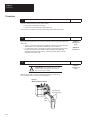
Allen-Bradley
SLC 500t
RTD/Resistance
Input Module
(Cat. No. 1746-NR4)
User
Manual
Important User
Information
Because of the variety of uses for the products described in this
publication, those responsible for the application and use of this
control equipment must satisfy themselves that all necessary steps
have been taken to assure that each application and use meets all
performance and safety requirements, including any applicable laws,
regulations, codes and standards.
The illustrations, charts, sample programs and layout examples
shown in this guide are intended solely for purposes of example.
Since there are many variables and requirements associated with any
particular installation, Allen-Bradley does not assume responsibility
or liability (to include intellectual property liability) for actual use
based upon the examples shown in this publication.
Allen-Bradley publication SGI-1.1, Safety Guidelines for the
Application, Installation, and Maintenance of Solid-State Control
(available from your local Allen-Bradley office), describes some
important differences between solid-state equipment and
electromechanical devices that should be taken into consideration
when applying products such as those described in this publication.
Reproduction of the contents of this copyrighted publication, in
whole or in part, without written permission of Allen-Bradley
Company, Inc., is prohibited.
Throughout this manual we use notes to make you aware of safety
considerations:
!
ATTENTION: Identifies information about practices
or circumstances that can lead to personal injury or
death, property damage or economic loss.
Attention statements help you to:
• identify a hazard
• avoid the hazard
• recognize the consequences
Important:
Identifies information that is critical for successful
application and understanding of the product.
PLC, PLC-2, PLC-3, and PLC-5 are registered trademarks of Allen–Bradley Company, Inc.
SLC, SLC 500, MicroLogix, PanelView, RediPANEL, and Dataliner are trademarks of Allen–Bradley Company, Inc.
IBM is a registered trademark of International Business Machines, Incorporated.
Belden is a trademark of Belden, Inc.
Summary of Changes
Summary of Changes
The information below summarizes the changes to this manual since the last
printing as 1746-6.7–January 1997.
To help you find new information and updated information in this release of
the manual, we have included change bars as shown to the right of this
paragraph.
New Information
The table below lists sections that document new features and additional
information about existing features, and shows where to find this new
information.
For This New Information
Calibration
Single-point calibration
See
page 3–13
page 3–14
Table of Contents
RTD/Resistance Input Module
User Manual
Preface
Who Should Use this Manual . . . . . . . . . . . . . . . . . . . . . . . . . . . . . . . . . . .
Purpose of this Manual . . . . . . . . . . . . . . . . . . . . . . . . . . . . . . . . . . . . . . . .
Contents of this Manual . . . . . . . . . . . . . . . . . . . . . . . . . . . . . . . . . . . . .
Related Documentation . . . . . . . . . . . . . . . . . . . . . . . . . . . . . . . . . . . . .
Terms and Abbreviations . . . . . . . . . . . . . . . . . . . . . . . . . . . . . . . . . . . . . .
Common Techniques Used in this Manual . . . . . . . . . . . . . . . . . . . . . . . . . .
Allen–Bradley Support . . . . . . . . . . . . . . . . . . . . . . . . . . . . . . . . . . . . . . . .
Local Product Support . . . . . . . . . . . . . . . . . . . . . . . . . . . . . . . . . . . . . .
Technical Product Assistance . . . . . . . . . . . . . . . . . . . . . . . . . . . . . . . . .
Your Questions or Comments on this Manual . . . . . . . . . . . . . . . . . . . . . .
Overview
P–1
P–1
P–2
P–3
P–4
P–6
P–6
P–6
P–7
P–7
Chapter 29
Description . . . . . . . . . . . . . . . . . . . . . . . . . . . . . . . . . . . . . . . . . . . . . . . . 1–1
RTD Compatibility . . . . . . . . . . . . . . . . . . . . . . . . . . . . . . . . . . . . . . . . . 1–3
Resistance Device Compatibility . . . . . . . . . . . . . . . . . . . . . . . . . . . . . . . 1–5
Hardware Overview . . . . . . . . . . . . . . . . . . . . . . . . . . . . . . . . . . . . . . . . 1–5
General Diagnostic Features . . . . . . . . . . . . . . . . . . . . . . . . . . . . . . . . . 1–6
System Overview . . . . . . . . . . . . . . . . . . . . . . . . . . . . . . . . . . . . . . . . . . . 1–7
System Operation . . . . . . . . . . . . . . . . . . . . . . . . . . . . . . . . . . . . . . . . . 1–8
Powerup . . . . . . . . . . . . . . . . . . . . . . . . . . . . . . . . . . . . . . . . . . . . . . 1–8
Module Operation . . . . . . . . . . . . . . . . . . . . . . . . . . . . . . . . . . . . . . . 1–8
LED Status . . . . . . . . . . . . . . . . . . . . . . . . . . . . . . . . . . . . . . . . . . . . 1–9
Module to Processor Communication . . . . . . . . . . . . . . . . . . . . . . . . . . . 1–10
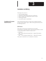
Quick Start Guide
Chapter 30
Required Tools and Equipment . . . . . . . . . . . . . . . . . . . . . . . . . . . . . . . . . .
Procedures . . . . . . . . . . . . . . . . . . . . . . . . . . . . . . . . . . . . . . . . . . . . . . . .
Installation and Wiring
2–1
2–2
Chapter 31
Compliance to European Union Directives . . . . . . . . . . . . . . . . . . . . . . . . . .
EMC Directive . . . . . . . . . . . . . . . . . . . . . . . . . . . . . . . . . . . . . . . . . . . .
Electrostatic Damage . . . . . . . . . . . . . . . . . . . . . . . . . . . . . . . . . . . . . . . . .
NR4 Power Requirements . . . . . . . . . . . . . . . . . . . . . . . . . . . . . . . . . . . . .
Module Location in Chassis . . . . . . . . . . . . . . . . . . . . . . . . . . . . . . . . . . . .
Modular Chassis Considerations . . . . . . . . . . . . . . . . . . . . . . . . . . . . . . .
Fixed Expansion Chassis Considerations . . . . . . . . . . . . . . . . . . . . . . . . .
General Considerations . . . . . . . . . . . . . . . . . . . . . . . . . . . . . . . . . . . . .
Module Installation and Removal . . . . . . . . . . . . . . . . . . . . . . . . . . . . . . . . .
Removing the Terminal Block . . . . . . . . . . . . . . . . . . . . . . . . . . . . . . . . .
Installing the Module . . . . . . . . . . . . . . . . . . . . . . . . . . . . . . . . . . . . . . .
Removing the Module . . . . . . . . . . . . . . . . . . . . . . . . . . . . . . . . . . . . . .
Terminal Wiring . . . . . . . . . . . . . . . . . . . . . . . . . . . . . . . . . . . . . . . . . . . . .
NR4 Wiring Considerations . . . . . . . . . . . . . . . . . . . . . . . . . . . . . . . . . . .
3–1
3–1
3–2
3–2
3–3
3–3
3–3
3–3
3–4
3–4
3–5
3–5
3–6
3–6
i
Table of Contents
RTD/Resistance Input Module
User Manual
Wiring Resistance Devices (Potentiometers) to the NR4 Module . . . . . . . .
Wiring Input Devices to the NR4 Module . . . . . . . . . . . . . . . . . . . . . . . . .
Calibration . . . . . . . . . . . . . . . . . . . . . . . . . . . . . . . . . . . . . . . . . . . . . . . .
Factory Calibration . . . . . . . . . . . . . . . . . . . . . . . . . . . . . . . . . . . . . . . . .
Autocalibration . . . . . . . . . . . . . . . . . . . . . . . . . . . . . . . . . . . . . . . . . . .
Single–Point Calibration . . . . . . . . . . . . . . . . . . . . . . . . . . . . . . . . . . . . .
Preliminary Operating
Considerations
Chapter 32
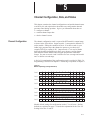
Channel Configuration,
Data, and Status
Chapter 33
ii
Module ID Code . . . . . . . . . . . . . . . . . . . . . . . . . . . . . . . . . . . . . . . . . . . .
Module Addressing . . . . . . . . . . . . . . . . . . . . . . . . . . . . . . . . . . . . . . . . . .
Output Image – Configuration Words . . . . . . . . . . . . . . . . . . . . . . . . . . . .
Input Image – Data Words and Status Words . . . . . . . . . . . . . . . . . . . . . .
Channel Filter Frequency Selection . . . . . . . . . . . . . . . . . . . . . . . . . . . . . . .
Channel Step Response . . . . . . . . . . . . . . . . . . . . . . . . . . . . . . . . . . . . .
Effective Resolution . . . . . . . . . . . . . . . . . . . . . . . . . . . . . . . . . . . . . . . .
Channel Cut–Off Frequency . . . . . . . . . . . . . . . . . . . . . . . . . . . . . . . . . .
Scanning Process and Channel Timing . . . . . . . . . . . . . . . . . . . . . . . . . . . .
Channel Autocalibration . . . . . . . . . . . . . . . . . . . . . . . . . . . . . . . . . . . . .
Update Time and Scanning Process . . . . . . . . . . . . . . . . . . . . . . . . . . . .
Channel Turn–On, Turn–Off, and Reconfiguration Times . . . . . . . . . . . . . . . .
Response to Slot Disabling . . . . . . . . . . . . . . . . . . . . . . . . . . . . . . . . . . . . .
Input Response . . . . . . . . . . . . . . . . . . . . . . . . . . . . . . . . . . . . . . . . . . .
Output Response . . . . . . . . . . . . . . . . . . . . . . . . . . . . . . . . . . . . . . . . . .
Channel Configuration . . . . . . . . . . . . . . . . . . . . . . . . . . . . . . . . . . . . . . . .
Channel Configuration Procedure . . . . . . . . . . . . . . . . . . . . . . . . . . . . . . . .
Configure Each Channel . . . . . . . . . . . . . . . . . . . . . . . . . . . . . . . . . . . .
Enter the Configuration Data . . . . . . . . . . . . . . . . . . . . . . . . . . . . . . . . . .
Input Type Selection (Bits 0–3) . . . . . . . . . . . . . . . . . . . . . . . . . . . . . . . .
Data Format Selection (Bits 4 and 5) . . . . . . . . . . . . . . . . . . . . . . . . . . . .
Using Scaled–For–PID and Proportional Counts Formats . . . . . . . . . . .
Scaling Examples . . . . . . . . . . . . . . . . . . . . . . . . . . . . . . . . . . . . . . .
Scaled–for–PID to Engineering Units . . . . . . . . . . . . . . . . . . . . . . . . . .
Engineering Units to Scaled–for–PID . . . . . . . . . . . . . . . . . . . . . . . . . .
Proportional Counts to Engineering Units . . . . . . . . . . . . . . . . . . . . . . .
Engineering Units to Proportional Counts . . . . . . . . . . . . . . . . . . . . . . .
Broken Input Selection (Bits 6 and 7) . . . . . . . . . . . . . . . . . . . . . . . . . . . .
Temperature Units Selection (Bit 8) . . . . . . . . . . . . . . . . . . . . . . . . . . . . .
Filter Frequency Selection (Bits 9 and 10) . . . . . . . . . . . . . . . . . . . . . . . .
Channel Enable Selection (Bit 11) . . . . . . . . . . . . . . . . . . . . . . . . . . . . . .
Excitation Current Selection (Bit 12) . . . . . . . . . . . . . . . . . . . . . . . . . . . .
Scaling Select (Bits 13–14) . . . . . . . . . . . . . . . . . . . . . . . . . . . . . . . . . . .
Default Scaling – . . . . . . . . . . . . . . . . . . . . . . . . . . . . . . . . . . . . . . . .
3–9
3–12
3–13
3–13
3–13
3–14
4–1
4–2
4–2
4–3
4–3
4–4
4–5
4–5
4–9
4–9
4–9
4–11
4–11
4–11
4–11
5–1
5–2
5–2
5–3
5–5
5–5
5–5
5–8
5–8
5–8
5–8
5–8
5–12
5–12
5–13
5–13
5–14
5–14
5–15
Table of Contents
RTD/Resistance Input Module
User Manual
User–set Scaling – . . . . . . . . . . . . . . . . . . . . . . . . . . . . . . . . . . . . . . .
Configuration Words For User–set Scaling (Words 4 to 7) . . . . . . . . . . .
Unused (Bit 15) . . . . . . . . . . . . . . . . . . . . . . . . . . . . . . . . . . . . . . . . . . .
Channel Data Word . . . . . . . . . . . . . . . . . . . . . . . . . . . . . . . . . . . . . . . . . .
Channel Status Checking . . . . . . . . . . . . . . . . . . . . . . . . . . . . . . . . . . . . . .
Input Type Status (Bits 0–3) . . . . . . . . . . . . . . . . . . . . . . . . . . . . . . . . . .
Data Format Status (Bits 4 and 5) . . . . . . . . . . . . . . . . . . . . . . . . . . . . . .
Broken Input Status (Bits 6 and 7) . . . . . . . . . . . . . . . . . . . . . . . . . . . . . .
Temperature Units Status (Bit 8) . . . . . . . . . . . . . . . . . . . . . . . . . . . . . . .
Channel Filter Frequency (Bits 9 and 10) . . . . . . . . . . . . . . . . . . . . . . . . .
Channel Enable Status (Bit 11) . . . . . . . . . . . . . . . . . . . . . . . . . . . . . . . .
Excitation Current (Bit 12) . . . . . . . . . . . . . . . . . . . . . . . . . . . . . . . . . . . .
Broken Input Error (Bit 13) . . . . . . . . . . . . . . . . . . . . . . . . . . . . . . . . . . .
Out–Of–Range Error (Bit 14) . . . . . . . . . . . . . . . . . . . . . . . . . . . . . . . . .
Configuration Error (Bit 15) . . . . . . . . . . . . . . . . . . . . . . . . . . . . . . . . . . .
Ladder Programming
Examples
Chapter 34
Module Diagnostics and
Troubleshooting
Chapter 35
Application Examples
Chapter 36
5–15
5–16
5–17
5–18
5–19
5–21
5–21
5–21
5–21
5–21
5–22
5–22
5–22
5–23
5–23
Device Configuration . . . . . . . . . . . . . . . . . . . . . . . . . . . . . . . . . . . . . . . . . 6–1
Initial Programming . . . . . . . . . . . . . . . . . . . . . . . . . . . . . . . . . . . . . . . . . . 6–2
Procedure . . . . . . . . . . . . . . . . . . . . . . . . . . . . . . . . . . . . . . . . . . . . . . . 6–3
Dynamic Programming . . . . . . . . . . . . . . . . . . . . . . . . . . . . . . . . . . . . . . . . 6–4
Procedure . . . . . . . . . . . . . . . . . . . . . . . . . . . . . . . . . . . . . . . . . . . . . . . 6–4
Verifying Channel Configuration Changes . . . . . . . . . . . . . . . . . . . . . . . . . . 6–5
Interfacing to the PID Instruction . . . . . . . . . . . . . . . . . . . . . . . . . . . . . . . . . 6–7
Using the Proportional Counts Data Format with the User–set Scaling . . . . . . 6–9
Monitoring Channel Status Bits . . . . . . . . . . . . . . . . . . . . . . . . . . . . . . . . . . 6–10
Invoking Autocalibration . . . . . . . . . . . . . . . . . . . . . . . . . . . . . . . . . . . . . . . 6–11
Module Operation vs. Channel Operation . . . . . . . . . . . . . . . . . . . . . . . . . . .
Power–Up Diagnostics . . . . . . . . . . . . . . . . . . . . . . . . . . . . . . . . . . . . . . . .
Channel Diagnostics . . . . . . . . . . . . . . . . . . . . . . . . . . . . . . . . . . . . . . . . .
LED Indicators . . . . . . . . . . . . . . . . . . . . . . . . . . . . . . . . . . . . . . . . . . . . . .
Error Codes . . . . . . . . . . . . . . . . . . . . . . . . . . . . . . . . . . . . . . . . . . . . . . .
Channel Status LEDs (Green) . . . . . . . . . . . . . . . . . . . . . . . . . . . . . . . . .
Invalid Channel Configuration . . . . . . . . . . . . . . . . . . . . . . . . . . . . . . .
Open– and Short–Circuit Detection . . . . . . . . . . . . . . . . . . . . . . . . . . .
Out–Of–Range Detection . . . . . . . . . . . . . . . . . . . . . . . . . . . . . . . . . .
Module Status LED (Green) . . . . . . . . . . . . . . . . . . . . . . . . . . . . . . . . . .
Replacement Parts . . . . . . . . . . . . . . . . . . . . . . . . . . . . . . . . . . . . . . . . . .
Contacting Allen–Bradley . . . . . . . . . . . . . . . . . . . . . . . . . . . . . . . . . . . . . .
Basic Example . . . . . . . . . . . . . . . . . . . . . . . . . . . . . . . . . . . . . . . . . . . . .
7–1
7–1
7–1
7–2
7–3
7–4
7–4
7–4
7–5
7–5
7–7
7–7
8–1
iii
Table of Contents
RTD/Resistance Input Module
User Manual
Channel Configuration . . . . . . . . . . . . . . . . . . . . . . . . . . . . . . . . . . . . . .
Program Listing . . . . . . . . . . . . . . . . . . . . . . . . . . . . . . . . . . . . . . . . . . .
Data Table . . . . . . . . . . . . . . . . . . . . . . . . . . . . . . . . . . . . . . . . . . . . . .
Supplementary Example . . . . . . . . . . . . . . . . . . . . . . . . . . . . . . . . . . . . . .
Channel Configuration . . . . . . . . . . . . . . . . . . . . . . . . . . . . . . . . . . . . . .
Program Setup and Operation Summary . . . . . . . . . . . . . . . . . . . . . . . . .
Program Listing . . . . . . . . . . . . . . . . . . . . . . . . . . . . . . . . . . . . . . . . . . .
Data Table . . . . . . . . . . . . . . . . . . . . . . . . . . . . . . . . . . . . . . . . . . . . . .
Specifications
Appendix A
Electrical Specifications . . . . . . . . . . . . . . . . . . . . . . . . . . . . . . . . . . . . . . .
Physical Specifications . . . . . . . . . . . . . . . . . . . . . . . . . . . . . . . . . . . . . . . .
Module Environmental Specifications . . . . . . . . . . . . . . . . . . . . . . . . . . . . .
Input Specifications . . . . . . . . . . . . . . . . . . . . . . . . . . . . . . . . . . . . . . . . . .
Module Accuracy . . . . . . . . . . . . . . . . . . . . . . . . . . . . . . . . . . . . . . . . . .
Resistance Device Compatibility . . . . . . . . . . . . . . . . . . . . . . . . . . . . . . .
Cable Specifications . . . . . . . . . . . . . . . . . . . . . . . . . . . . . . . . . . . . . . .
RTD Standards
Appendix B
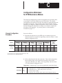
Configuration Worksheet
for RTD/Resistance Module
Appendix C
iv
8–1
8–3
8–3
8–4
8–5
8–7
8–8
8–9
Channel Configuration Procedure . . . . . . . . . . . . . . . . . . . . . . . . . . . . . . . .
A–1
A–1
A–2
A–2
A–3
A–5
A–5
C–1
Preface
Preface
Read this preface to familiarize yourself with the rest of the manual. This
preface covers the following topics:
• who should use this manual
• the purpose of this manual
• terms and abbreviations
• conventions used in this manual
• Allen–Bradley support
Who Should Use this
Manual
Use this manual if you are responsible for designing, installing,
programming, or troubleshooting control systems that use Allen–Bradley
small logic controllers.
You should have a basic understanding of SLC 500t products. You should
understand programmable controllers and be able to interpret the ladder logic
instructions required to control your application. If you do not, contact your
local Allen–Bradley representative for information on available training
courses before using this product. If using Advanced Programming Software
(APS), we recommend that you review The APS Quick Start for New Users,
Publication 9399-APSQS.
Purpose of this Manual
This manual is a reference guide for the 1746–NR4 RTD/Resistance Input
Module. The manual:
• gives you an overview of system operation
• explains the procedures you need to install and wire the module at the
customer site
• provides ladder programming examples
• provides an application example of how this input module can be used to
control a process
P–1
Preface
Contents of this Manual
Chapter
Contents
Preface
Describes the purpose, background, and scope of
this manual. Also specifies the audience for whom
this manual is intended and defines key terms and
abbreviations used throughout this book.
1
Overview
Provides a hardware and system overview.
Explains and illustrates the theory behind the RTD
input module.
2
Quick Start Guide
Provides a general procedural roadmap to help you
get started using the RTD module.
3
Installation and Wiring
Provides installation procedures and wiring
guidelines.
4
Preliminary Operating
Considerations
Gives you the background information you need to
understand how to address and configure the
module for optimum operation as well as how to
make changes once the module is in a run state.
5
Channel Configuration,
Data, and Status
Examines the channel configuration word and the
channel status word bit by bit, and explains how the
module uses configuration data and generates
status during operation.
6
Ladder Programming Examples
Gives an example of the ladder logic required to
define the channel for operation. Also includes
representative examples for unique programming
requirements such as PID.
7
Module Diagnostics and
Troubleshooting
Explains how to interpret and correct problems with
your RTD module.
Application Examples
Examines both basic and supplementary
applications and gives examples of the ladder
programming necessary to achieve the desired
result.
Appendix A
Specifications
Provides physical, electrical, environmental, and
functional specifications for the RTD module.
Appendix B
RTD Standards
Provides physical, electrical, environmental, and
functional specifications for the RTD and
potentiometer.
Appendix C
Configuration Worksheet
for RTD/Resistance Module
Provides a worksheet to help you configure the
module for operation.
8
P–2
Title
Preface
Preface
Related Documentation
The following documents contain information that may be helpful to you as
you use Allen–Bradley SLCt products. To obtain a copy of any of the
Allen–Bradley documents listed, contact your local Allen–Bradley office or
distributor.
For
Read this Document
Document
Number
An overview of the SLC 500 family of products
SLC 500 System Overview
1747–2.30
A description on how to install and use your Modular SLC 500
programmable controller
Installation & Operation Manual for Modular Hardware
Style Programmable Controllers
1747–6.2
A description on how to install and use your Fixed SLC 500
programmable controller
Installation & Operation Manual for Fixed Hardware Style
Programmable Controllers
1747–6.21
A procedural manual for technical personnel who use APS to develop
control applications
Rockwell Software Advanced Programming Software
(APS) User Manual
9399-APSUM
A reference manual that contains status file data, instruction set, and
troubleshooting information about APS
SLC 500t and MicroLogix 1000t Instruction Set
Reference Manual
1747–6.15
An introduction to APS for first–time users, containing basic concepts but
focusing on simple tasks and exercises, and allowing the reader to begin
programming in the shortest time possible
APS Quick Start for New Users
9399-APSQS
A procedural and reference manual for technical personnel who use an
HHT to develop control applications
Allen-Bradley Hand-Held Terminal User’s Manual
1747–NP002
An introduction to HHT for first–time users, containing basic concepts but
focusing on simple tasks and exercises, and allowing the reader to begin
programming in the shortest time possible
Getting Started Guide for HHT
1747–NM009
A resource manual and user’s guide containing information about the
analog modules used in your SLC 500 system.
SLC 500 Analog I/O Modules User’s Manual
1746–6.4
In–depth information on grounding and wiring Allen–Bradley
programmable controllers
Allen-Bradley Programmable Controller Grounding and
Wiring Guidelines
1770–4.1
A description of important differences between solid–state programmable
controller products and hard–wired electromechanical devices
Application Considerations for Solid–State Controls
SGI–1.1
A complete listing of current AllenBradley documentation, including
ordering instructions. Also indicates whether the documents are
available on CD–ROM or in multi–languages.
Allen-Bradley Publication Index
SD499
A glossary of industrial automation terms and abbreviations
Allen-Bradley Industrial Automation Glossary
AG–7.1
National Electrical Code
Published by the
National Fire
Protection
Association of
Boston, MA.
An article on wire sizes and types for grounding electrical equipment
P–3
Preface
Terms and Abbreviations
The following terms and abbreviations are specific to this product. For a
complete listing of Allen–Bradley terminology, refer to the Allen–Bradley
Industrial Automation Glossary, Publication Number AG–7.1.
A/D – Refers to the analog–to–digital converter inherent to the
RTD/Resistance input module. The converter produces a digital value whose
magnitude is proportional to the instantaneous magnitude of an analog input
signal.
attenuation – The reduction in the magnitude of a signal as it passes through
a system.
channel – Refers to one of four small–signal analog input interfaces
available on the module’s terminal block. Each channel is configured for
connection to an RTD or potentiometer input device and has its own
diagnostic status word.
chassis – A hardware assembly that houses devices such as I/O modules,
adapter modules, processor modules, and power supplies.
common mode rejection ratio – The ratio of a device’s differential voltage
gain to common mode voltage gain, expressed in dB.
CMRR = 20 Log10 (V1/V2)
common mode voltage – A voltage signal induced in conductors with
respect to ground (0 potential).
configuration word – Contains the channel configuration information
needed by the module to configure and operate each channel. Information is
written to the configuration word through the logic supplied in your ladder
program.
cut–off frequency – The frequency at which the input signal is attenuated
3dB by the digital filter. Frequency components of the input signal below the
cut–off frequency are passed with under 3dB of attenuation.
data word – A 16–bit integer that represents the value of the analog input
channel. The channel data word is valid only when the channel is enabled
and there are no channel errors. When the channel is disabled, the channel
data word is cleared (0).
dB (decibel) – A logarithmic measure of the ratio of two signal levels.
digital filter – A low–pass noise filter incorporated into the A/D converter.
In addition, the digital filter provides high–rejection notches at frequencies
that are integral multiples of the filter cut–off frequency. The notches are
used for rejecting AC power line noise and higher frequency noise.
excitation current – A user–selectable current (0.5 mA and 2.0 mA) that the
module sends through the RTD or resistive device to produce an analog
signal which the NR4 can process and convert to temperature or to ohms,
respectively.
P–4
Preface
Preface
effective resolution – The amount of jitter (data variation) that typically
occurs in the data word due to the influence of the internal electrical noise in
the module.
filter frequency – The user–selectable first–notch frequency for the A/D
converter’s digital filter. The digital filter provides AC power line noise
rejection when the first notch is at 10 Hz or at the power line frequency.
full scale error (gain error) – The difference in slope between the actual and
ideal potentiometer or RTD transfer functions.
full scale range (FSR) – The difference between the maximum and
minimum specified analog RTD or resistive input values.
gain drift – The change in full scale transition voltage measured over the
operating temperature range of the module.
input data scaling –The data formats that you select to define the logical
increments of the channel data word. These may be scaled–for–PID, or
Engineering Units for RTD or potentiometer inputs, which are automatically
scaled. They may also be proportional counts, which you must calculate to
fit your application’s temperature or resistance resolution.
local configuration – A control system where all the chassis are located
within several feet of the processor and chassis–to–chassis communication is
via a 1746–C7 or 1746–C9 ribbon cable.
LSB (Least Significant Bit) – Refers to a data increment defined as the full
scale range divided by the resolution. The LSB represents the smallest value
within a string of bits.
multiplexer – A switching system that allows several input signals to share a
common A/D converter.
normal mode rejection (differential mode rejection) – A logarithmic
measure in dB, of a device’s ability to reject noise signals between or among
circuit signal conductors, but not between equipment grounding conductor or
signal reference structure and the signal conductors.
potentiometer (Pot) – A variable resistor that can be connected to the RTD
module.
remote configuration – A control system where the chassis can be located
several thousand feet from the processor chassis. Chassis communication is
via the 1747–SN Scanner and 1747–ASB Remote I/O Adapter.
resolution – The smallest detectable change in a measurement, typically
expressed in engineering units (e.g., 0.1 °C) or as a number of bits. For
example, a 12–bit system has 4,096 possible output states. It can, therefore,
measure 1 part in 4096.
RTD (Resistance Temperature Detector) – A temperature sensing element
with 2, 3 or 4 lead wires. It uses the basic characteristic that electrical
P–5
Preface
resistance of metals increases with temperature. When a small current is
applied to the RTD, it creates a voltage that varies with temperature. This
voltage is processed and converted by the RTD module into a temperature
value.
sampling time – The time required by the A/D converter to sample an input
channel.
status word – Contains status information about the channel’s current
configuration and operational state. You can use this information in your
ladder program to determine whether the channel data word is valid.
step response time – This is the time required for the A/D input signal to
reach 100% of its expected final value, given a large step change in the input
signal.
update time – The time required for the module to sample and convert the
input signals of all enabled input channels and make the resulting data values
available to the SLC processor.
Common Techniques Used in
this Manual
The following conventions are used throughout this manual:
• Bulleted lists such as this one provide information, not procedural steps.
• Numbered lists provide sequential steps or hierarchical information.
• Italic type is used for emphasis.
• Text in this font indicates words or phrases you should type.
Allen–Bradley Support
Allen–Bradley offers support services worldwide, with over 75 Sales/Support
Offices, 512 authorized Distributors and 260 authorized Systems Integrators
located throughout the United States alone, plus Allen–Bradley
representatives in every major country in the world.
Local Product Support
Contact your local Allen–Bradley representative for:
• sales and order support
• product technical training
• warranty support
• support service agreements
Technical Product Assistance
If you need to contact Allen–Bradley for technical assistance, please review
the information in the Module Diagnostics and Troubleshooting chapter first.
Then call your local Allen–Bradley representative.
P–6
Preface
Preface
Your Questions or Comments on this Manual
If you find a problem with this manual, please notify us of it on the enclosed
Publication Problem Report.
If you have any suggestions for how this manual could be made more useful
to you, please contact us at the address below:
Allen–Bradley Company, Inc.
Control and Information Group
Technical Communication, Dept. A602V, T122
P.O. Box 2086
Milwaukee, WI 53201–2086
P–7
Chapter
1
Overview
This chapter describes the 4–channel 1746–NR4 RTD/Resistance Input
Module and explains how the SLC controller gathers RTD (Resistance
Temperature Detector) temperature or resistance–initiated analog input from
the module. Included is:
• general description of the module’s hardware and software features
• an overview of system operation
For the rest of the manual, the 1746–NR4 RTD/Resistance Input Module will
be referred to as simply the RTD module.
Description
The RTD module receives and stores digitally converted analog data from
RTDs or other resistance inputs such as potentiometers into its image table
for retrieval by all fixed and modular SLC 500 processors. An RTD consists
of a temperature–sensing element connected by 2, 3, or 4 wires that provide
input to the RTD module. The module supports connections from any
combination of up to four RTDs of various types (for example: platinum,
nickel, copper, or nickel–iron) or other resistance inputs.
As shown in Figure 1.1, the RTD module supplies a small current to each
RTD connected to the module inputs (up to 4 input channels). The module
provides on–board scaling and converts RTD input to temperature (°C, °F) or
reports resistance input in ohms.
Each input channel is individually configurable for a specific input device.
Broken sensor detection (open– or short–circuit) is provided for each input
channel. In addition, the module provides indication if the input signal is
out–of–range. For more detail on module functionality refer to the
subsection entitled System Overview later in this chapter.
1–1
Chapter 1
Overview
Figure 1.1
Simplified RTD Module Circuit
Constant Current Source
IC= 0.5 or 2 mA
RTD Module
RTD
Sense
Backplane
RTD0
Return
RTD
Sense
RTD1
Return
RTD
Sense
RTD2
Return
RTD
Sense
RTD3
1–2
Return
A/D
Conversion
Digital Data
µP Circuit
Digital Data
Chapter 1
Overview
RTD Compatibility
Table 1.A lists the RTD types you can use with the RTD module and gives
each type’s associated temperature range, resolution, and repeatability
specifications. Table 1.B shows the accuracy and temperature drift
specifications for the RTDs.
Table 1.A
RTD Temperature Ranges, Resolution, and Repeatability
Temp. Range
(0.5 mA Excitation)➁
–200 °C to +850 °C
(–328 °F to +1562 °F)
Temp. Range
(2.0 mA Excitation)➁
–200 °C to +850 °C
(–328 °F to +1562 °F)
200W
–200 °C to +850 °C
(–328 °F to +1562 °F)
–200 °C to +850 °C
(–328 °F to +1562 °F)
0.1 °C
(0.2 °F)
500W
–200 °C to +850 °C
(–328 °F to +1562 °F)
–200 °C to +850 °C
(–328 °F to +1562 °F)
0.1 °C
(0.2 °F)
1000W
–200 °C to +850 °C
(–328 °F to +1562 °F)
–200 °C to +240 °C
(–328 °F to +464 °F)
0.1 °C
(0.2 °F)
100W
–200 °C to +630 °C
(–328 °F to +1166°F)
–200 °C to +630 °C
(–328 °F to +1166 °F)
0.1 °C
(0.2 °F)
200W
–200 °C to +630 °C
(–328 °F to +1166°F)
–200 °C to +630 °C
(–328 °F to +1166 °F)
0.1 °C
(0.2 °F)
500W
–200 °C to +630 °C
(–328 °F to +1166°F)
–200 °C to +630 °C
(–328 °F to +1166 °F)
0.1 °C
(0.2 °F)
1000W
–200 °C to +630 °C
(–328 °F to +1166°F)
–200 °C to +230 °C
(–328 °F to +446 °F)
RTD Type
100Ω
Pai
Platinum
(385)➀
385 ➀
Pai
3916 ➀
Platinum
(3916)➀
Resolution
Repeatability
0.1 °C
(0.2 °F)
0.1 °C
(0.2 °F)
0.2 °C
( 0.4 °F)
0.2 °C
( 0.4 °F)
0.2 °C
( 0.4 °F)
0.2 °C
( 0.4 °F)
0.2 °C
( 0.4 °F)
0.2 °C
( 0.4 °F)
0.2 °C
( 0.4 °F)
0.2 °C
( 0.4 °F)
Copper (426)➀➂
10W
Not allowed.➄
–100 °C to +260 °C
(–148 °F to +500 °F)
0.1 °C
(0.2 °F)
0.2 °C
( 0.4 °F)
Nickel (618)➀➃
120W
–100 °C to +260 °C
(–148 °F to +500 °F)
–100 °C to +260 °C
(–148 °F to +500 °F)
0.1 °C
(0.2 °F)
0.1 °C
( 0.2 °F)
Nickel (672)➀
120W
–80 °C to +260 °C
(–112 °F to +500 °F)
–80 °C to +260 °C
(–112 °F to +500 °F)
0.1 °C
(0.2 °F)
0.1 °C
( 0.2 °F)
Nickel Iron (518)➀
604W
–100 °C to +200 °C
(–148 °F to +392 °F)
–100 °C to +200 °C
(–148 °F to +392 °F)
0.1 °C
(0.2 °F)
0.1 °C
( 0.2 °F)
➀
➁
➂
➃
➄
The digits following the RTD type represent the temperature coefficient of resistance (α), which is defined as the resistance change
per ohm per °C. For instance, Platinum 385 refers to a platinum RTD with α = 0.00385 ohms/ohm –°C or simply 0.00385 /°C.
The temperature range for the 1000W RTD is dependant on the excitation current.
Actual value at 0 °C is 9.042W per SAMA standard RC21–4–1966.
Actual value at 0 °C is 100W per DIN standard.
To maximize the relatively small RTD signal, only 2 mA excitation current is allowed.
Important: The exact signal range valid for each input type is dependent
upon the excitation current magnitude that you select when
configuring the module. For details on excitation current, refer
to page A–2.
1–3
Chapter 1
Overview
Table 1.B
RTD Accuracy and Temperature Drift Specifications
RTD Type
100W
200W
Pai
385 ➀
Platinum
(385)➀
500W
1000W
100W
200W
Pai
3916 ➀
Platinum
(3916)➀
500W
1000W
Accuracy➁
(0.5 mA Excitation)
1.0 °C
( 2.0 °F)
1.0 °C
( 2.0 °F)
0.6 °C
( 1.1 °F)
0.6 °C
( 1.1 °F)
1.0 °C➆
( 2.0 °F)
1.0 °C➆
( 2.0 °F)
0.5 °C
( 0.9 °F)
0.5 °C
( 0.9 °F)
Accuracy➁
(2.0 mA Excitation)
0.5 °C
( 0.9 °F)
0.5 °C
( 0.9 °F)
0.5 °C
( 0.9 °F)
0.5 °C
( 0.9 °F)
0.4 °C
( 0.7 °F)
0.4 °C
( 0.7 °F)
0.4 °C
( 0.7 °F)
0.4 °C
( 0.7 °F)
Temperature Drift➅
(0.5 mA Excitation)
0.034 °C/°C
( 0.061 °F/°F)
0.034 °C/°C
( 0.061 °F/°F)
0.017 °C/°C
( 0.031 °F/°F)
0.017 °C/°C
( 0.031 °F/°F)
0.034 °C/°C
( 0.061 °F/°F)
0.034 °C/°C
( 0.061 °F/°F)
0.014 °C/°C
( 0.025 °F/°F)
0.014 °C/°C
( 0.025 °F/°F)
Temperature Drift➅
(2.0 mA Excitation)
0.014 °C/°C
( 0.025 °F/°F)
0.014 °C/°C
( 0.025 °F/°F)
0.014 °C/°C
( 0.025 °F/°F)
0.014 °C/°C
( 0.025 °F/°F)
0.011 °C/°C
( 0.020 °F/°F)
0.011 °C/°C
( 0.020 °F/°F)
0.011 °C/°C
( 0.020 °F/°F)
0.011 °C/°C
( 0.020 °F/°F)
Copper (426)➀➂
10W
Not allowed.➄
0.6 °C
( 1.1 °F)
Not allowed.➄
0.017 °C/°C
( 0.031 °F/°F)
Nickel (618)➀➃
120W
0.2 °C
( 0.4 °F)
0.2 °C
( 0.4 °F)
0.008 °C/°C
( 0.014 °F/°F)
0.008 °C/°C
( 0.014 °F/°F)
Nickel (672)➀
120W
0.2 °C
( 0.4 °F)
0.2 °C
( 0.4 °F)
0.008 °C/°C
( 0.014 °F/°F)
0.008 °C/°C
( 0.014 °F/°F)
Nickel Iron (518)➀
604W
0.3 °C
( 0.5 °F)
0.3 °C
( 0.5 °F)
0.010 °C/°C
( 0.018 °F/°F)
0.010 °C/°C
( 0.018 °F/°F)
➀ The digits following the RTD type represent the temperature coefficient of resistance (α), which is defined as the resistance change per
ohm per °C. For instance, Platinum 385 refers to a platinum RTD with α = 0.00385 ohms/ohm –°C or simply 0.00385 /°C.
➁ The accuracy values assume that the module was calibrated within the specified temperature range of 0°C to 60°C (32°F to 140°F).
➂ Actual value at 0 °C is 9.042W per SAMA standard RC21–4–1966.
➃ Actual value at 0 °C is 100W per DIN standard.
➄ To maximize the relatively small RTD signal, only 2 mA excitation current is allowed.
➅ Temperature drift specifications apply to a module that has not been calibrated.
When you are using 100W or 200W platinum RTDs with 0.5 mA excitation
current, refer to the following important note about module accuracy.
Important:
Module accuracy, using 100W or 200W platinum RTDs with 0.5
mA excitation current, depends on the following criteria:
• Module accuracy is 0.6 °C after you apply power to the module or
perform an autocalibration at 25 °C ambient with module operating
temperature at 25 °C.
• Module accuracy is (0.6 °C + DT 0.034 °C/°C) after you apply
power to the module or perform an autocalibration at 25 °C ambient with
the module operating temperature between 0° to 60 °C.
– where DT is the temperature difference between the actual operating
temperature of the module and 25 °C and 0.034 °C/°C is the
temperature drift shown in the table above for 100W or 200W platinum
RTDs.
• Module accuracy is 1.0 °C after you apply power to the module or
perform an autocalibration at 60 °C ambient with module operating
temperature at 60 °C.
1–4
Chapter 1
Overview
Resistance Device Compatibility
Table 1.C lists the resistance input types you can use with the RTD module
and gives each type’s associated specifications.
Table 1.C
Resistance Input Specifications
150W
Resistance Range
(0.5 mA Excitation)
0 W to 150 W
Resistance Range
(2.0 mA Excitation)
0 W to 150 W
500W
0 W to 500 W
0 W to 500 W
0.5W
1000W
0 W to 1000 W
0 W to 1000 W
1.0W
3000W
0 W to 3000 W
0 W to 1900 W
1.5W
Input Type
Resistance
Accuracy➂
Temperature Drift
Resolution
Repeatability
➀
➁
0.014 W/°C
( 0.025 W/°F)
0.029 W/°C
( 0.052 W/°F)
0.01W
0.04W
0.1W
0.2W
0.1W
0.2W
0.1W
0.2W
0.043 W/°C
( 0.077 W/°F)
➀ The accuracy for 150Ω is dependant on the excitation current:
0.2Ω at 0.5 mA
0.15Ω at 2.0 mA
➁ The temperature drift for 150Ω is dependant on the excitation current:
0.006Ω/°C at 0.5 mA
0.004Ω at 2.0 mA
➂ The accuracy values assume that the module was calibrated within the specified temperature range of 0°C to 60°C (32°F to 140°F).
Hardware Overview
The RTD module fits into a single–slot of an SLC 500:
• modular system, except the processor slot (0)
• fixed system expansion chassis (1746–A2)
The module uses eight input words and eight output words.
Important: If the RTD module resides in a remote configuration with a SLC
500 Remote I/O Adapter Module (1747–ASB), use block
transfer for configuration and data retrieval. Block transfer
requires a 1747–SN Remote I/O Scanner (Series B) or PLC
processor.
As shown in Figure 1.2 and Table 1.D, the module contains a removable
terminal block (item 3) providing connection for any mix of four RTD
sensors or resistance input devices. There are no output channels on the
module. Module configuration is done via the user program. There are no
DIP switches.
1–5
Chapter 1
Overview
Figure 1.2
RTD Module Hardware
6
1
INPUT
5
MODULE STATUS
2
RTD/resistance
3
SHIELD
RETRN
SHIELD
CHL 2
RTD
SHIELD
CHL 3
RETRN
SHIELD
SHIELD
INPUT SIGNAL RANGES
RTD TYPES:
PLATINUM, COPPER
NICKEL, NICKEL–IRON
4
150 Ω , 500 Ω , 1000 Ω , 3000 Ω
RETRN
RESISTANCE:
CHL 3
CHL 2 RTD
SENSE
CHL 3
CHL 2 SENSE
SA
CHL 1
CHL 0 RTD
SENSE
CHL 1
CHL 0 SENSE
RETRN CHL 1
OPERATING
TEMPERATURE
CODE T3C
CLASS I, GROUPS A, B, C AND D, DIV.2
SHIELD
CHL 0
RTD
SLC 500
RTD/resistance INPUT MODULE
SER U LISTED IND. CONT. EQ.
L FOR HAZ. LOC. A196
2
3
CAT
1746 NR4
0
1
FRN
SERIAL NO.
NR4–xxx x
CHANNEL
STATUS
7
Table 1.D
Hardware Features
1
Channel Status LED
Indicators (green)
Display operating and fault status of
channels 0, 1, 2, and 3
2
Module Status LED (green)
Displays module operating and fault status
3
Removable Terminal Block
Provides physical connection to input devices (Part
# 1746–RT25G)
4
Cable Tie Slots
Secure wiring from module
5
Door Label
Provides terminal identification
6
Side Label (Nameplate)
Provides module information
7
Self–Locking Tabs
Secure module in chassis slot
General Diagnostic Features
The RTD module contains diagnostic features that can be used to help you
identify the source of problems that may occur during power up or during
normal channel operation. These power–up and channel diagnostics are
explained in chapter 7, Module Diagnostics and Troubleshooting.
1–6
Chapter 1
Overview
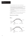
System Overview
The RTD module communicates to the SLC 500 processor through the
parallel backplane interface and receives +5V dc and +24V dc power from
the SLC 500 power supply through the backplane. No external power supply
is required. You may install as many RTD modules in your system as the
power supply can support, as shown in Figure 1.3.
Figure 1.3
RTD Configuration
RTD Modules
SLC Processor
Each individual channel on the RTD module can receive input signals from
2, 3 or 4–wire RTD sensors or from resistance input devices. You configure
each channel to accept either input. When configured for RTD input types,
the module converts the RTD readings into linearized, digital temperature
readings in °C or °F. When configured for resistance inputs, the module
provides a linear resistance value in ohms.
Important: The RTD module is designed to accept input from RTD sensors
with up to 3 wires. When using 4–wire RTD sensors, one of the
2 lead compensation wires is not used and the 4–wire sensor is
treated like a 3–wire sensor. Lead wire compensation is
provided via the third wire. See NR4 Wiring Considerations on
page 3–6 for more information.
1–7
Chapter 1
Overview
System Operation
The RTD module has 3 operational states:
• power–up
• module operation
• error (module error and channel error)
Power–up
At power–up, the RTD module checks its internal circuits, memory, and
basic functions via hardware and software diagnostics. During this time the
module status LED remains off. If no faults are found during the power–up
diagnostics, the module status LED is turned on.
After power–up checks are complete, the RTD module waits for valid
channel configuration data from your SLC ladder logic program (channel
status LEDs off). After configuration data is written to one or more channel
configuration words and their channel enable bits are set by the user
program, the channel status LEDs go on and the module continuously
converts the RTD or resistance input to a value within the range you selected
for the enabled channels. The module is now operating in its normal state.
Each time a channel is read by the module, that data value is tested by the
module for a fault condition, for example, open circuit, short circuit, over
range, and under range. If such a condition is detected, a unique bit is set in
the channel status word and the channel status LED blinks, indicating a
channel error condition.
The SLC processor reads the converted RTD or resistance data from the
module at the end of the program scan or when commanded by the ladder
program. The processor and RTD module determine that the backplane data
transfer was made without error and the data is used in your ladder program.
Module Operation
Referring to Figure 1.1, each input channel consists of an RTD connection,
which provides:
• excitation current
• a sense connection, which detects lead–wire resistance
• a return connection, which reads the RTD or resistance value
Each of these analog inputs are multiplexed to 1 of 2 analog convertors.
The A/D convertors cycle between reading the RTD or resistance value, the
lead wire resistance, and the excitation current. From these readings, an
accurate temperature or resistance is returned to the user program.
The RTD module is isolated from the chassis backplane and chassis ground.
The isolation is limited to 500V dc. Optocouplers are used to communicate
across the isolation barrier. Channel–to–channel common–mode isolation is
limited to 1 volt.
1–8
Chapter 1
Overview
LED Status
Figure 1.4 shows the RTD module LED panel consisting of 5 LEDs. The
state of the LEDs (for example, off, on, or blinking) depends on the
operational state of the module (see Table 1.E).
Figure 1.4
LED Indicators
INPUT
CHANNEL
STATUS
0
2
1
3
MODULE STATUS
RTD/resistance
RTD MODULE
The purpose of the LEDs is as follows:
• Channel Status – One LED for each of the 4 input channels indicates if
the channel is enabled, disabled, or is not operating as configured, due to
an error (Table 1.E).
• Module Status – If OFF at any time, other than at powerup, this LED
indicates that non–recoverable module errors (for example, diagnostic or
operating errors) have occurred. The LED is ON if there are no module
errors.
The status of each LED, during each of the operational states (for example,
powerup, module operation and error), is depicted in the following table.
Table 1.E
LED
POWER–UP
MODULE OPERATION
(No Error)
MODULE ERROR
CHANNEL ERROR
Ch 0 Status
Off➁
On/Off➀
Off
Blinks
Ch 1 Status
Off➁
On/Off➀
Off
Blinks
Ch 2 Status
Off➁
On/Off➀
Off
Blinks
Ch 3 Status
Off➁
On/Off➀
Off
Blinks
Mod. Status
Off➁
On
Off
On
➀ Channel status LED is On if the respective channel is enabled and Off if the channel is disabled.
➁ Module is disabled during powerup.
1–9
Chapter 1
Overview
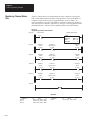
Module to Processor Communication
As shown in Figure 1.5, the RTD module communicates with the SLC
processor through the backplane of the chassis. The RTD module transfers
data to / receives data from the processor by means of an image table. The
image table (Table 1.F) consists of 8 input words and 8 output words. Data
transmitted from the module to the processor is called the input image (for
example, Channel Data Words and Channel Status Words). Conversely, data
transmitted from the processor to the module is called the output image (for
example, Channel Configuration Words and Scaling Limit Words). Details
about the input and output images are found in Module Addressing on page
4–2 and 4–3.
Figure 1.5
Communication Flow
Channel Data Words
Channel Status Words
1746–NR4
Input
Module
RTD/resistance
Analog Signals
SLC 500
Processor
Scaling Limit Words
Channel Configuration Words
Chassis Backplane
Table 1.F
Image Table
Input Image Word
Function
Output Image Word
Function
0
Channel 0 data
0
Channel 0 configuration
1
Channel 1 data
1
Channel 1 configuration
2
Channel 2 data
2
Channel 2 configuration
3
Channel 3 data
3
Channel 3 configuration
4
Channel 0 status
4
User–set Lower limit scale 0
5
Channel 1 status
5
User–set Upper limit scale 0
6
Channel 2 status
6
User–set Lower limit scale 1
7
Channel 3 status
7
User–set Upper limit scale 1
The Channel Configuration Words (output image) contain user–defined
configuration information for the specified input channel. This information
is used by the module to configure and operate each channel. The Channel
Status Words (input image) contain status information about the channel’s
current configuration and operational state. The input data values of the
analog input channel are contained in the Channel Data Word (input image),
which is valid only when the channel is enabled and there are no channel
errors (for example, broken sensor or overrange.)
The user–set Scaling Limit Words (output image) provide a user–definable
scaling range for the temperature resistance data when using the proportional
counts data type.
1–10
Chapter
2
Quick Start Guide
This chapter helps you get started using the RTD module. The procedures
included here assume that you have a basic understanding of SLC 500
products.
You must:
• understand electronic process control
• be able to interpret the ladder logic instructions for generating the
electronic signals that control your application
Because it is a start–up guide, this chapter does not contain detailed
explanations about the procedures listed. It does, however, reference other
chapters in this book where you can get more detailed information.
If you have any questions or are unfamiliar with the terms used or concepts
presented in the procedural steps, always read the referenced chapters and
other recommended documentation before trying to apply the information.
This chapter:
• tells you what equipment you need
• explains how to install and wire the module
• shows you how to set up one channel for RTD or resistance input.
• examines the state of the LEDs at normal startup
• examines the channel status word
Required Tools and
Equipment
Have the following tools and equipment ready:
• medium blade screwdriver
• medium cross–head screwdriver
• RTD module (1746–NR4)
• RTD sensor or resistance input
• appropriate cable (if needed)
• programming equipment (All programming examples shown in this
manual demonstrate the use of Advanced Programming Software [APS]
for personal computers.)
2–1
Chapter 2
Quick Start
Procedures
1.
Procedure: Unpacking Module
Unpack the module making sure that the contents include:
• RTD module (Catalog Number 1746–NR4)
• Installation instructions (Publication Number 1746–5.17)
Reference
–
If the contents are incomplete, call your local Allen–Bradley representative for assistance.
2.
Procedure: Determining Power Requirements
Review the power requirements of your system to see that your chassis supports placement of the
RTD module.
• The fixed, 2–slot chassis supports two RTD modules. If combining an RTD module with a
different module, refer to the module compatibility table found in chapter 3.
• For modular style systems, calculate the total load on the system power supply using the
procedure described in the SLC Installation & Operation Manual for Modular Style
Controllers (Publication Number 1747–6.2) or the SLC 500 Family System Overview
(Publication Number 1747–2.30).
3.
Procedure: Inserting Module
!
ATTENTION: Never install, remove, or wire
modules with power applied to the chassis or
devices wired to the module.
Make sure system power is off; then insert the RTD module into your 1746 chassis.
In this example procedure, local slot 1 is selected (Figure 2.1).
Figure 2.1
Module Insertion Into Chassis
Top and Bottom
Module Release(s)
Card
Guide
2–2
Reference
Chapter 3
(Installation and
Wiring)
Appendix A
(Specifications)
Reference
Chapter 3
(Installation and
Wiring)
Chapter 2
Quick Start
4.
Procedure: Wiring Module
Reference
Connect RTD (Figure 2.2) or potentiometer (Figure 2.3 or Figure 2.4) wire leads to channel 0 of the
RTD module.
Chapter 3
(Installation and
Wiring)
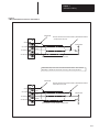
Figure 2.2
RTD Connections To Terminal Block
For details on wiring an RTD to the module,
see chapter 3.
2–Wire RTD Interconnection
Add Jumper
Cable Shield
Shield
Chl 0 RTD
RTD
RTD
Return
Return
Chl 0 Sense
Chl 0 Return
Terminal Pin–outs
Shield
Beldent #9501 Shielded Cable
Chl 0
RTD
3–Wire RTD Interconnection
Cable Shield
Shield
Chl 0 RTD
Chl 0 Sense
Chl 0 Return
RTD
RTD
Sense
Sense
Return
Return
Beldent #83503 or Beldent #9533 Shielded Cable
4–Wire RTD Interconnection
Cable Shield
Shield
Chl 1
Chl 0 RTD
Sense Chl 1
Chl 0 Sense
Return Chl 1
Return
Shield
Shield
Chl 2
RTD
Chl 3
Chl 2 RTD
Sense Chl 3
Chl 2 Sense
Return Chl 3
Return
Shield
Shield
Shield
Chl 0 RTD
Chl 0 Sense
Chl 0 Return
RTD
RTD
Sense
Sense
Return
Return
Belden #83503 or Belden #9533 Shielded Cable
Leave One Sensor Wire Open
2–3
Chapter 2
Quick Start
Figure 2.3
2–Wire Potentiometer Connections To Terminal Block
For details on wiring a potentiometer
to the module, see chapter 3.
Cable Shield
Add Jumper
Potentiometer
Shield
Chl 0 RTD
RTD
Chl 0 Sense
Chl 0 Return
Return
Belden #9501 Shielded Cable
Potentiometer wiper arm can be connected to either the RTD or return terminal
depending on whether the user wants increasing or decreasing resistance.
Add Jumper
Shield
Chl 0 RTD
RTD
Potentiometer
Chl 0 Sense
Chl 0 Return
Return
Belden #9501 Shielded Cable
2–4
Chapter 2
Quick Start
Figure 2.4
3–Wire Potentiometer Connections To Terminal Block
For details on wiring a potentiometer
to the module, see chapter 3.
Cable Shield
Run RTD and sense wires from module to potentiometer terminal
and tie them to one point.
Shield
Chl 0 RTD
Potentiometer
RTD
Sense
Chl 0 Sense
Chl 0 Return
Return
Belden #83503 or Belden #9533 Shielded Cable
Potentiometer wiper arm can be connected to either the RTD or return terminal
depending on whether the user wants increasing or decreasing resistance.
Cable Shield
Run RTD and sense wires from module to potentiometer terminal
and tie them to one point.
Shield
Chl 0 RTD
RTD
Potentiometer
Sense
Chl 0 Sense
Chl 0 Return
Return
Belden #83503 or Belden #9533 Shielded Cable
2–5
Chapter 2
Quick Start
5.
Procedure: Configuring Your I/O
Reference
Configure your system I/O configuration for the particular slot where the RTD module resides (slot 1 in
this example). Using APS software, select the 1746–NR4 from the list of modules, or if it is not listed
in your software version, select Other and enter the RTD module ID code (3513) at the prompt on
the I/O configuration display.
Chapter 4
(Preliminary
Operating
Considerations)
No manual entry of special I/O configuration (SPIO CONFIG) information is required, as the
module ID code automatically assigns the number of input and output words required by the module.
(Additional information about how to configure your system can be found in the APS Quick Start for
New Users, Publication 9399-APSQS.)
Example of Software Prompt:
Press ENTER to select I/O Module
Enter Module ID Code> 3513
offline
SLC 5/02
SELECT
MODULE
F2
2–6
File EXAMPLE
Chapter 2
Quick Start
6.
Procedure: Configuring the Module
Reference
Determine the operating parameters for channel 0. In this example, Figure 2.5 shows the channel 0
configuration word defined with all defaults (0) except for channel enable (bit 11). The addressing
reflects the location of the module as slot 1. For details on how to configure the module for your
application, refer to chapters 4 and 5.
(A configuration worksheet is included on page C–4 to assist you in channel configuration.)
Chapter 4
(Preliminary
Operating
Considerations)
Chapter 5
(Channel
Configuration,
Data, and Status)
O:1.0
O:1.1
O:1.2
O:1.3
O:1.4
O:1.5
O:1.6
O:1.7
Word 0
Word 1
Channel 0 Configuration Word
Channel 1 Configuration Word
Word 2
Channel 2 Configuration Word
Word 3
Channel 3 Configuration Word
Word 4
User–set Lower Scale Limit Range 0
Word 5
User–set Upper Scale Limit Range 0
Word 6
User–set Lower Scale Limit Range 1
Word 7
User–set Upper Scale Limit Range 1
Input Type Select
Data Format Select
Broken Input Select
Temperature Units Select
Address
Filter Frequency Select
Output Image
(8 words)
Excitation Current Select
Channel Enable
Input Image
Not Defined
SLC 500 Controller
Data Files
Scaling Select *
Figure 2.5
Output Image Detail
0 0 0 0 0 0 0 0 0 0 0 0 0 0 0 0
Bit 15
Bit 0
* Scaling Select bits apply to proportional counts mode.
Limit Scale Words are only used if scaling select = 01 or
10 and data format = 11.
Default Settings
• 100 W Platinum RTD (385)
• Engineering Units x 1 (0.1° / step)
• Broken Input (set data word to zero)
• Degrees Celsius (° C)
• 10 Hz. Filter Frequency
• Channel Disabled
• 2.0 mA Excitation Current
• Module Defined Scaling
If proportional counts data format is used, then output words 4–7
can be used to define a user–set scaling range for each channel.
Bit 15
Bit 0
0 0 0 0 1 0 0 0 0 0 0 0 0 0 0 0
New Setting
Set this bit (11) to enable channel. Address = O:1.0/11.
2–7
Chapter 2
Quick Start
7.
Procedure: Programming the Configuration
Reference
Do the programming necessary to establish the new configuration word setting in the previous step.
1. Using the memory map function, create integer file N10. Integer file N10 should contain one
element for each channel used. (For this example we only need one, N10:0.)
2. Using the APS, enter the configuration parameters from step 6 for channel 0 into integer
N10:0. In this example, all the bits of N10:0 will be zero except for the channel enable
(N10:0/11).
3. Program an instruction in your ladder logic to copy the contents of N10:0 to output word
O:1.0 (Figure 2.6).
Figure 2.6
Initial Configuration Word Setting
Example of Data Table for Integer File N10:
address
N10:0
15
data
0
0000 1000 0000 0000
First Pass Bit
S:1
] [
15
2–8
address
COP
COPY FILE
Source
# N10:0
Dest
Length
# O:1.0
1
15
data
0
On power–up, the first pass bit
(S:1/15) is set for one scan, enabling
the COPY instruction that transfers a
one to bit 11 of channel configuration
word 0. This enables channel 0,
which directs the RTD module to scan
channel 0 and to present the analog
data to the SLC processor.
Chapter 6
(Ladder
Programming
Examples)
Chapter 8
(Application
Examples)
Chapter 2
Quick Start
8.
Procedure: Write Remaining Ladder Logic
Reference
As shown in Figure 2.7, the Channel Data Word contains the information that represents the
temperature value or resistance value of the input channel. Write the remainder of the ladder logic
program that specifies how your RTD/resistance input data will be processed for your application. In
this procedure, the addressing reflects the location of the module as slot 1.
(Complete information about how to do ladder programming using the APS software can be found in
the APS User Manual, Publication 9399-APSUM.)
Chapter 5
(Channel
Configuration,
Data, and Status)
Chapter 6
(Ladder
Programming
Examples)
Chapter 8
(Application
Examples)
your programming
software’s user
manual
Figure 2.7
Input Image Detail
SLC 500 Controller
Data Files
Input Image
(8 words)
Output Image
Address
Address
I:1.0
I:1.1
I:1.2
I:1.3
Word 0
Word 1
Word 2
Word 3
.
.
.
.
.
.
I:1.7 Word 7
Channel 0 Data Word
Channel 1 Data Word
Channel 2 Data Word
Channel 3 Data Word
Channel 0 Status Word
Channel 1 Status Word
Channel 2 Status Word
Channel 3 Status Word
I:1.0
0 0 0 0 0 0 0 0 0 0 0 0 0 0 0 0
Bit 15
(Variable RTD/resistance Input Data)
Bit 0
2–9
Chapter 2
Quick Start
9.
Procedure: Test Your RTD Program
Apply power. Download your program to the SLC and put the controller into Run mode. In this example during a normal start up, the module status LED (Figure 2.8) and channel 0 status LED turn on.
Figure 2.8
LED Status
INPUT
CHANNEL
STATUS
0
2
1
3
MODULE STATUS
RTD/resistance
2–10
Channel LEDs
Module Status LED
Reference
Chapter 7
(Module
Diagnostics and
Troubleshooting)
Chapter 2
Quick Start
10.
Procedure: Program Functional Check (Optional)
Reference
(Optional) Monitor the status of input channel 0 to determine its configuration setting and operational
status (Figure 2.9). This is useful for troubleshooting when the blinking channel LED indicates that an
error has occurred. If the Module Status LED is off, or if the Channel 0 LED is off or blinking, refer to
chapter 7.
Chapter 5
(Channel
Configuration,
Data, and Status)
Chapter 7
(Module
Diagnostics and
Troubleshooting)
Chapter 8
(Application
Examples)
Figure 2.9
Monitoring Status
SLC 500 Controller
Data Files
Channel 3 Data Word
.
.
Word 7
Channel 0 Status Word
Channel 1 Status Word
Channel 2 Status Word
Channel 3 Status Word
Input Type
Channel 2 Data Word
Word 3
Data Format
Word 2
Broken Input
Channel 0 Data Word
Channel 1 Data Word
Temperature Units
Word 0
Word 1
Filter Frequency
Output Image
Configuration Error
Out–Of–Range Error
Broken Input Error
Excitation Current
Channel Status
Input Image
(8 words)
0 0 0 0 1 0 0 0 0 0 0 0 0 0 0 0
Bit 15
Address
Bit 0
I:1.4
For this example, only bit 11 is set during normal operation.
2–11
Chapter
3
Installation and Wiring
This chapter tells you how to:
• avoid electrostatic damage
• determine the RTD module’s chassis power requirement
• choose a location for the RTD module in the SLC chassis
• install the RTD module
• wire the RTD module’s terminal block
Compliance to European
Union Directives
If this product has the CE mark it is approved for installation within the
European Union and EEA regions. It has been designed and tested to meet
the following directives.
EMC Directive
This product is tested to meet Council Directive 89/336/EEC
Electromagnetic Compatibility (EMC) and the following standards, in whole
or in part, documented in a technical construction file:
• EN 50081-2
EMC – Generic Emission Standard, Part 2 – Industrial Environment
• EN 50082-2
EMC – Generic Immunity Standard, Part 2 – Industrial Environment
This product is intended for use in an industrial environment.
3–1
Chapter 3
Installation and Wiring
Electrostatic Damage
Electrostatic discharge can damage semiconductor devices inside this module
if you touch backplane connector pins or other sensitive areas. Guard against
electrostatic damage by observing the precautions listed next.
!
ATTENTION: Electrostatic discharge can degrade performance
or cause permanent damage. Handle the module as stated below.
• Wear an approved wrist strap grounding device when handling the
module.
• Touch a grounded object to rid yourself of electrostatic charge before
handling the module.
• Handle the module from the front, away from the backplane connector.
Do not touch backplane connector pins.
• Keep the module in its static–shield bag when not in use, or during
shipment.
NR4 Power Requirements
The RTD module receives its power through the SLC500 chassis backplane
from the fixed or modular +5V dc/+24V dc chassis power supply. The
maximum current drawn by the module is shown in the table below.
5V dc Amps
24V dc Amps
0.050
0.050
When you are using a modular system configuration, add the values shown in
the table above to the requirements of all other modules in the SLC chassis to
prevent overloading the chassis power supply.
When you are using a fixed system controller, refer to the Important note
about module compatibility in a 2–slot expansion chassis on page NO TAG.
3–2
Chapter 3
Installation and Wiring
Module Location in Chassis
Fixed Controller Compatibility Table
NR4
IA4
IA8
IA16
IM4
IM8
IM16
OA8
OA16
OAP12
IB8
IB16
IV8
IV16
IG16
IH16
OV8
OV16
OB8
OBP8
OG16
OW4
OW8
OW16
IO4
IO8
IO12
NI4
NI8
NIO4I
NIO4V
FIO4I
FIO4V
DCM
HS
OB16
OB16E
IN16
BASn
BAS
OB32
OV32
IV32
IB32
OX8
NO4I
NO4V
ITB16
ITV16
IC16
KE
KEn
OBP16
OVP16
NT4
NR4
HSTP1
•
•
•
•
•
•
•
•
•
•
•
•
•
•
•
•
•
•
•
•
•
•
•
•
•
•
•
•
•
•
•
•
•
•
•
•
•
•
•
•
•
∇
•
•
•
•
•
•
•
•
•
•
•
5V dc
(Amps)
24V dc
(Amps)
0.035
0.050
0.085
0.035
0.050
0.085
0.185
0.370
0.370
0.050
0.085
0.050
0.085
0.140
0.085
0.135
0.270
0.135
0.135
0.180
0.045
0.085
0.170
0.030
0.060
0.090
0.025
0.200
0.055
0.055
0.055
0.055
0.360
0.300
0.280
0.135
0.085
0.150
0.150
0.452
0.452
0.106
0.106
0.085
0.055
0.055
0.085
0.085
0.085
0.150
0.150
0.250
0.250
0.060
0.050
0.200
0.045
0.090
0.180
0.025
0.045
0.070
0.085
0.100
0.145
0.115
0.150
0.120
0.125
0.040
0.090
0.195
0.145
0.040
0.145
0.040
0.050
-
Modular Chassis Considerations
Place your RTD module in any slot of an SLC 500 modular chassis (except
slot 0) or a modular expansion chassis. Slot 0 is reserved for the modular
processor or adapter modules.
Fixed Expansion Chassis Considerations
Important: The 2–slot, SLC 500 fixed I/O expansion chassis (1746–A2)
supports only specific combinations of modules. If you are
using the RTD module in a 2–slot expansion chassis with
another SLC I/O or communication module, refer to the table at
the left to determine whether the combination can be supported.
In the table:
•
A dot indicates a valid combination.
No symbol indicates an invalid combination.
∇
A triangle indicates an external power supply is required.
(Refer to the Analog I/O Module User Manual, 1746–6.4.)
When using the table, be aware that there are certain conditions
that affect the compatibility characteristics of the BASIC
module (BAS) and the DH–485/RS–232C module (KE).
When you use the BAS module or the KE module to supply
power to a 1747–AIC Link Coupler, the link coupler draws its
power through the module. The higher current drawn by the
AIC at 24V dc is calculated and recorded in the table for the
modules identified as BASn (BAS networked) or KEn (KE
networked). Make sure to refer to these modules if your
application uses the BAS or KE module in this way.
General Considerations
Most applications require installation in an industrial enclosure to reduce the
effects of electrical interference. RTD inputs are susceptible to electrical
noises due to the small amplitudes of their signal.
Group your modules to minimize adverse effects from radiated electrical
noise and heat. Consider the following conditions when selecting a slot for
the RTD module. Position the module in a slot:
• away from power lines, load lines and other sources of electrical noise
such as hard–contact switches, relays, and AC motor drives
• away from modules which generate significant radiated heat, such as the
32–point I/O modules
3–3
Chapter 3
Installation and Wiring
Module Installation and
Removal
When installing the module in a chassis, it is not necessary to remove the
terminal block from the module. However, if the terminal block is removed,
use the write–on label located on the side of the terminal block, as shown
below, to identify the module location and type.
SLOT ____
•
RACK ____
MODULE _______________
Removing the Terminal Block
!
ATTENTION: Never install, remove, or wire modules with power
applied to the chassis or devices wired to the module.
To avoid cracking the removable terminal block alternate the
removal of the slotted terminal block release screws.
1. Loosen the two terminal block release screws (Figure 3.1).
Figure 3.1
Terminal Block Release Screws
Terminal Block Release Screws
Max. Torque = 0.6 Nm (5.3 in–lbs)
2. Grasp the terminal block at the top and bottom and pull outward and
down.
3–4
Chapter 3
Installation and Wiring
Installing the Module
1. Align the circuit board of the RTD module with the card guides located at
the top and bottom of the chassis as shown in the following figure.
Figure 3.2
Module Insertion Into the Chassis
Top and Bottom
Module Release(s)
Card
Guide
2. Slide the module into the chassis until both top and bottom retaining clips
are secured. Apply firm even pressure on the module to attach it to its
backplane connector. Never force the module into the slot.
3. Cover all unused slots with the Card Slot Filler, Catalog Number
1746–N2.
Removing the Module
1. Press the releases at the top and bottom of the module and slide the
module out of the chassis slot.
2. Cover all unused slots with the Card Slot Filler, Catalog Number
1746–N2.
3–5
Chapter 3
Installation and Wiring
Terminal Wiring
The RTD module contains an 18–position, removable terminal block. The
terminal pin–out is shown in Figure 3.3.
!
ATTENTION: Disconnect power to the SLC before attempting
to install, remove, or wire the removable terminal wiring block.
To avoid cracking the removable terminal block, alternate the
removal of the terminal block release screws.
Figure 3.3
Terminal Block
(Terminal Block Spare Part Catalog Number 1746–RT25G)
Shield
Release Screw
Max. Torque = 0.6 Nm (5.3 in–lbs)
Shield
Channel 0 RTD
Channel 1 RTD
Channel 0 Sense
Channel 1 Sense
Channel 0 Return
Channel 1 Return
Shield
Shield
Channel 2 RTD
Channel 3 RTD
Channel 2 Sense
Channel 3 Sense
Channel 2 Return
Channel 3 Return
Shield
Shield
Release Screw
Max. Torque =
0.6 Nm (5.3 in–lbs)
NR4 Wiring Considerations
Follow the guidelines below when planning your system wiring.
Since the operating principle of the RTD module is based on the
measurement of resistance, take special care in selecting your input cable.
For 2-wire or 3-wire configuration, select a cable that has a consistent
impedance throughout its entire length.
Configuration
2-wire
3-wire
less than 30.48 m (100 ft)
3-wire
greater than 30.48 m (100 ft) or high humidity
conditions
Recommended Cable
Beldent #9501 or equivalent
Belden #9533 or equivalent
Belden #83503 or equivalent
For a 3-wire configuration, the module can compensate for a maximum cable
length associated with an overall cable impedance of 25 ohms.
Important: Details of cable specifications are shown on page A–5.
3–6
Chapter 3
Installation and Wiring
As shown in Figure 3.4, three configurations of RTDs can be connected to
the RTD module, namely:
• 2–wire RTD, which is composed of 2 RTD lead wires (RTD and Return)
• 3–wire RTD, which is composed of a Sense and 2 RTD lead wires (RTD
and Return)
• 4–wire RTD, which is composed of 2 Sense and 2 RTD lead wires (RTD
and Return). The second sense wire of a 4–wire RTD is left open. It does
not matter which sense wire is left open.
Important: The RTD module requires three wires to compensate for lead
resistance error. We recommend that you do not use 2–wire
RTDs if long cable runs are required, as it will reduce the
accuracy of the system. However, if a 2–wire configuration is
required, reduce the effect of the lead wire resistance by using a
lower gauge wire for the cable (for example, use AWG #16
instead of AWG #24). Also, use cable that has a lower
resistance per foot of wire. The module’s terminal block
accepts two AWG #14–gauge wires.
• To limit overall cable impedance, keep input cables as short as possible.
•
•
•
•
•
Locate your I/O chassis as near the RTD sensors as your application will
permit.
Ground the shield drain wire at one end only. The preferred location is at
the RTD module. Refer to IEEE Std. 518, Section 6.4.2.7 or contact your
sensor manufacturer for additional details.
Each input channel has a shield connection screw terminal that provides a
connection to chassis ground. All shields are internally connected, so any
shield terminal can be used with channels 0–3.
Route RTD/resistance input wiring away from any high–voltage I/O
wiring, power lines, and load lines.
Tighten terminal screws using a flat or cross–head screwdriver. Each
screw should be turned tight enough to immobilize the wire’s end.
Excessive tightening can strip the terminal screw. The torque applied to
each screw should not exceed 0.565 Nm (5 in–lb) for each terminal.
Follow system grounding and wiring guidelines found in your SLC 500
Installation and Operation Manual, publication 1747–6.2.
3–7
Chapter 3
Installation and Wiring
Figure 3.4
RTD Connections To Terminal Block
2–Wire RTD Interconnection
Add Jumper
Cable Shield
Shield
Chl 0 RTD
RTD
RTD
Return
Return
Chl 0 Sense
Chl 0 Return
Terminal Pin–outs
Shield
Belden #9501 Shielded Cable
Chl 0
RTD
3–Wire RTD Interconnection
Cable Shield
Shield
Chl 0 RTD
Chl 0 Sense
Chl 0 Return
RTD
RTD
Sense
Sense
Return
Return
Belden #83503 or Belden #9533 Shielded Cable
4–Wire RTD Interconnection
Cable Shield
Shield
Chl 0 RTD
Chl 0 Sense
Chl 0 Return
RTD
RTD
Sense
Sense
Return
Return
Belden #83503 or Belden #9533 Shielded Cable
Leave One Sensor Wire Open
3–8
Shield
Chl 1
Chl 0 RTD
Sense Chl 1
Chl 0 Sense
Return Chl 1
Return
Shield
Shield
Chl 2
RTD
Chl 3
Chl 2 RTD
Sense Chl 3
Chl 2 Sense
Return Chl 3
Return
Shield
Shield
Chapter 3
Installation and Wiring
When using a 3–wire configuration, the module compensates for resistance
error due to lead wire length . For example, in a 3–wire configuration, the
module reads the resistance due to the length of one of the wires and assumes
that the resistance of the other wire is equal. If the resistances of the
individual lead wires are much different, an error may exist. The closer the
resistance values are to each other, the greater the amount of error that is
eliminated.
Important: To ensure temperature or resistance value accuracy, the
resistance difference of the cable lead wires must be
equal to or less than 0.01Ω.
There are several ways to insure that the lead values match as closely as
possible. They are as follows:
• Keep lead resistance as small as possible and less than 25 Ω..
• Use quality cable that has a small tolerance impedance rating.
• Use a heavy–gauge lead wire which has less resistance per foot.
Wiring Resistance Devices (Potentiometers) to the NR4 Module
Potentiometer wiring requires the same type of cable as that for the RTD
described in the previous subsection. Potentiometers can be connected to the
RTD module as a 2–wire interconnection (Figure 3.5) or a 3–wire
interconnection (Figure 3.6).
3–9
Chapter 3
Installation and Wiring
Figure 3.5
2–Wire Potentiometer Connections To Terminal Block
2–Wire Potentiometer Interconnection
Cable Shield
Add Jumper
Potentiometer
Shield
Chl 0 RTD
RTD
Chl 0 Sense
Chl 0 Return
Return
Belden #9501 Shielded Cable
Potentiometer wiper arm can be connected to either the RTD or return terminal
depending on whether the user wants increasing or decreasing resistance.
Add Jumper
Shield
Chl 0 RTD
RTD
Potentiometer
Chl 0 Sense
Chl 0 Return
Return
Belden #9501 Shielded Cable
3–10
Chapter 3
Installation and Wiring
Figure 3.6
3–Wire Potentiometer Connections To Terminal Block
Cable Shield
Run RTD and sense wires from module to potentiometer terminal
and tie them to one point.
Shield
Chl 0 RTD
Potentiometer
RTD
Sense
Chl 0 Sense
Chl 0 Return
Return
Belden #83503 or Belden #9533 Shielded Cable
Potentiometer wiper arm can be connected to either the RTD or return terminal
depending on whether the user wants increasing or decreasing resistance.
Cable Shield
Run RTD and sense wires from module to potentiometer terminal
and tie them to one point.
Shield
Chl 0 RTD
RTD
Potentiometer
Sense
Chl 0 Sense
Chl 0 Return
Return
Belden #83503 or Belden #9533 Shielded Cable
3–11
Chapter 3
Installation and Wiring
To wire your NR4 module, follow these steps as shown in Figure 3.7:
1. At each end of the cable, strip some casing to expose the individual wires.
2. Trim the signal wires to 5.08–cm (2–inch) lengths. Strip about 4.76 mm
(3/16 inch) of insulation away to expose the end of the wire.
3. At one end of the cable twist the drain wire and foil shield together, bend
them away from the cable, and apply shrink wrap. Then earth ground at
the shield terminal.
4. At the other end of the cable, cut the drain wire and foil shield back to the
cable and apply shrink wrap.
5. Connect the signal wires and cable shield to the NR4 terminal block and
the input.
6. Repeat steps 1 through 5 for each channel on the NR4 module.
Wiring Input Devices to the NR4 Module
Figure 3.7
Shielded Cable
2–Conductor Shielded Cable
(See step 4.)
Signal Wire
Signal Wire
Drain Wire
(See step 3.)
Foil Shield
Signal Wire
Signal Wire
3–Conductor Shielded Cable
Signal Wire
(See step 4.)
Signal Wire
Signal Wire
Signal Wire
Drain Wire
(See step 3.)
3–12
Foil Shield
Signal Wire
Signal Wire
Chapter 3
Installation and Wiring
Calibration
The accuracy of a system that uses the RTD module is determined by the
following:
• the accuracy of the RTD
• resistance mismatch of the cable wires that connect the RTD to the
module
• the accuracy of the RTD module
For optimal performance at the customer site, the RTD module is calibrated
at the factory prior to shipment. In addition, a self–calibration feature, called
autocalibration, further ensures that the module performs to specification
over the life of the product.
Factory Calibration
The 4–pin calibration connector, on the RTD module circuit board, is used
for factory setup only.
Autocalibration
When a channel becomes enabled, the module configures the channel and
performs an autocalibration on the channel. The channel is selected, the
excitation current is turned off, and the three input lines for the channel are
connected to analog common. The module’s A/D converters are configured
for the proper gain and filter frequency that is appropriate for your RTD
configuration. Autocalibration performs an A/D conversion on the zero
voltage (analog common) and the full–scale voltage (A/D reference voltage)
on the following signals:
• lead wire signal
• RTD/resistance signal
• excitation current signal
Important: Channel calibration time is shown in Table 4.C.
These conversions generate offset (zero reference) and full scale (span
reference) coefficients that are saved and used by the module to perform
future A/D conversions on this channel.
You can command your module to perform an autocalibration cycle by
disabling a channel, waiting for the channel status bit to change state (1 to 0)
and then re–enabling that channel. Several scan cycles are required to
perform an autocalibration (refer to page 4–11). It is important to remember
that during autocalibration the module is not converting input data.
3–13
Chapter 3
Installation and Wiring
Tip
To maintain system accuracy we recommend that you periodically perform
an autocalibration cycle, for example:
• whenever an event occurs that greatly changes the internal temperature of
the control cabinet, such as opening or closing its door
• at a convenient time when the system is not making product, such as
during a shift change
An autocalibration programming example is provided in chapter 6.
Single–Point Calibration
Single–point calibration is an optional procedure that can be used to improve
the accuracy of the RTD module and cable combination to greater than
+/–0.2°C (when the RTD is operating at +/–50°C of the calibration
temperature). The offset, determined by the single–point calibration, can be
used to compensate for inaccuracies in the RTD module and cable
combination.
After single–point calibration is performed, additional calibrations only need
to be performed if the cable is disturbed or degraded. (RTD replacement
should not affect the accuracy of the procedure.) However, periodic
autocalibrations should be performed. Follow the steps below to perform a
single–point calibration:
1. Cycle power to the SLC 500 chassis.
2. Select a calibration temperature that is near the control point (+/–10°C).
3. Determine the exact resistance (+/–0.01 ohm) equivalent to the calibration
temperature by using a published temperature vs. resistance chart.
4. Replace the RTD with the fixed-precision resistor. (We recommend you
use a 2 ppm temperature coefficient resistor.)
5. Use the RTD module to determine the temperature equivalent to the fixed
precision resistor and cable combination.
6. Calculate the offset value by subtracting the calculated calibration
temperature from the measured temperature.
7. Reconnect the RTD to the cable.
8. Use ladder logic to apply (subtract) the offset from the measured
temperature to obtain corrected temperature.
3–14
Chapter
4
Preliminary Operating Considerations
This chapter explains how the RTD module and the SLC processor
communicate through the module’s input and output image. It lists the
preliminary setup and operation required before the RTD module can
function in a 1746 I/O system. Topics discussed include how to:
• enter the module ID code
• address your RTD module
• select the proper input filter for each channel
• calculate the RTD module update time
• interpret the RTD module response to slot disabling
Module ID Code
The module identification code is a unique number encoded for each 1746
I/O module. The code defines for the processor the type of I/O or specialty
module residing in a specific slot in the 1746 chassis. With APS version 5.0
or later, select the 1746–NR4 RTD module from the list of modules on the
system I/O configuration display to automatically enter the ID code. With
earlier versions of APS (version 1.04 through 4.02.01), you must manually
enter the module identification code when configuring the slot.
To manually enter the module ID code, select (other) from the list of
modules on the system I/O configuration display. The module ID code for
the RTD module is shown below:
Catalog Number
ID Code
1746–NR4
3513
No special I/O configuration (SPIO CONFIG) information is required. The
module ID code automatically assigns the correct number of input and output
words.
4–1
Chapter 4
Preliminary Operating Considerations
Module Addressing
The memory map shown in Figure 4.1 displays how the output and input
image tables are defined for the RTD module.
Figure 4.1
Memory Map
Bit 15
RTD Module
Image Table
SLC 5/0X
Data Files
Slot e
Output
Scan
Output Image
Output Image
8 Words
Output Image
Bit 0
Address
Channel 0 Configuration Word
Word 0
O:e.0
Channel 1 Configuration Word
Word 1
O:e.1
Channel 2 Configuration Word
Word 2
O:e.2
Channel 3 Configuration Word
Word 3
O:e.3
User–set Lower Scale Limit Range 0 Word 4
O:e.4
User–set Upper Scale Limit Range 0 Word 5
O:e.5
User–set Lower Scale Limit Range 1 Word 6
O:e.6
User–set Upper Scale Limit Range 1 Word 7
O:e.7
Input
Scan
Address
Slot e
Input Image
Input Image
8 Words
(Class 1)
Input Image
Channel 0 Data Word
Word 0
I:e.0
Channel 1 Data Word
Word 1
I:e.1
Channel 2 Data Word
Word 2
I:e.2
Channel 3 Data Word
Word 3
I:e.3
Channel 0 Status Word
Word 4
I:e.4
Channel 1 Status Word
Word 5
I:e.5
Channel 2 Status Word
Word 6
I:e.6
Word 7
I:e.7
Channel 3 Status Word
Bit 15
Bit 0
Output Image – Configuration Words
The 8–word, RTD module output image (defined as the output from the CPU
to the RTD module) contains information that you configure to define the
way a specific channel on the RTD module will work. These words take the
place of configuration DIP switches on the module. Although the RTD
output image is eight words long, only output words 0–3 are used to define
the operation of the module; output words 4–7 are used for special user–set
scaling using the proportional counts data format. Each output word 0–3
configures a single channel.
Example – If you want to configure channel 2 on the RTD module located in
slot 4 in the SLC chassis, your address would be O:4.2.
Slot
File Type
Word
O:4.2
Element
Delimiter
Word
Delimiter
Chapter 5, Channel Configuration, Data, and Status, gives you detailed bit
information about the data content of the configuration word.
4–2
Chapter 4
Preliminary Operating Considerations
Input Image – Data Words and Status Words
The 8–word, RTD module input image (defined as the input from the RTD
module to the CPU) represents data words and status words.
Input words 0–3 (data words) hold the input data that represent the
temperature value of the RTD input or ohmic value of the resistance inputs
for channels 0–3. This data word is valid only when the channel is enabled
and there are no channel errors.
Input words 4–7 (status words) contain the status of channels 0–3
respectively. The status bits for a particular channel reflect the configuration
settings that you have entered into the output image configuration word for
that channel and provide information about the channel’s operational state.
To receive valid status information, the channel must be enabled and the
channel must have processed any configuration changes that may have been
made to the configuration word.
Example – To obtain the status of channel 2 (input word 6) of the RTD
module located in slot 3 in the SLC chassis, use address I:3.6.
File Type
Slot
Word
I:3.6
Element Delimiter
Word Delimiter
Chapter 5, Channel Configuration, Data, and Status, gives you detailed bit
information about the content of the data word and the status word.
Channel Filter Frequency
Selection
The RTD module uses a digital filter that provides noise rejection for the
input signals. The digital filter is programmable, allowing you to select from
four filter frequencies for each channel. The digital filter provides the
highest noise rejection at the selected filter frequency.
Selecting a low value (for example, 10 Hz) for the channel filter frequency
provides greater noise rejection for a channel, but also increases the channel
update time. Selecting a high value for the channel filter frequency provides
lesser noise rejection, but decreases the channel update time.
Table 4.A on page 4–4 shows the available filter frequencies, as well as the
associated minimum normal mode rejection (NMR), cut–off frequency, and
step response for each filter frequency. The figures on pages 4–7 and 4–8
show the input channel frequency response for each filter frequency
selection.
4–3
Chapter 4
Preliminary Operating Considerations
Channel Step Response
The channel filter frequency determines the channel’s step response. The
step response is the time required for the analog input signal to reach 100%
of its expected final value. This means that if an input signal changes faster
than the channel step response, a portion of that signal will be attenuated by
the channel filter. Table 4.A shows the step response for each filter
frequency.
Table 4.A
Notch Frequencies
4–4
Cut–Off
Frequency
50 Hz NMR
60 Hz NMR
10 Hz
100 dB
100 dB
2.62 Hz
300 msec
50 Hz
100 dB
–
13.1 Hz
60 msec
60 Hz
–
100 dB
15.72 Hz
50 msec
250 Hz
–
–
65.5 Hz
12 msec
Filter Frequency
Step Response
Chapter 4
Preliminary Operating Considerations
Effective Resolution
The effective resolution for an input channel depends upon the filter
frequency selected for that channel. The following table displays the
effective resolution for the various input types and filter frequencies:
Table 4.B
Effective Resolution for RTD and Resistance Inputs
Input T
Type
pe
Filter Frequency
10 Hz
50 Hz
60 Hz
250 Hz
100W Pt RTD (385)➀
0.1 °C
(0.2 °F)
0.2 °C
(0.4 °F)
0.2 °C
(0.4 °F)
0.4 °C
(0.7 °F)
200W Pt RTD (385)➀
0.1 °C
(0.2 °F)
0.2 °C
(0.4 °F)
0.2 °C
(0.4 °F)
0.4 °C
(0.7 °F)
500W Pt RTD (385)➀
0.1 °C
(0.2 °F)
0.2 °C
(0.4 °F)
0.2 °C
(0.4 °F)
0.4 °C
(0.7 °F)
1000W Pt RTD (385)➀
0.1 °C
(0.2 °F)
0.2 °C
(0.4 °F)
0.2 °C
(0.4 °F)
0.4 °C
(0.7 °F)
100W Pt RTD (3916)➀
0.1 °C
(0.2 °F)
0.2 °C
(0.4 °F)
0.2 °C
(0.4 °F)
0.3 °C
(0.5 °F)
200W Pt RTD (3916)➀
0.1 °C
(0.2 °F)
0.2 °C
(0.4 °F)
0.2 °C
(0.4 °F)
0.3 °C
(0.5 °F)
500W Pt RTD (3916)➀
0.1 °C
(0.2 °F)
0.2 °C
(0.4 °F)
0.2 °C
(0.4 °F)
0.3 °C
(0.5 °F)
1000W Pt RTD (3916)➀
0.1 °C
(0.2 °F)
0.2 °C
(0.4 °F)
0.2 °C
(0.4 °F)
0.3 °C
(0.5 °F)
10W Cu RTD (426)➀➁
0.2 °C
(0.4 °F)
0.3 °C
(0.5 °F)
0.3 °C
(0.5 °F)
0.4 °C
(0.7 °F)
120W Ni RTD (618)➀➂
0.1 °C
(0.2 °F)
0.1 °C
(0.2 °F)
0.1 °C
(0.2 °F)
0.2 °C
(0.4 °F)
120W Ni RTD (672)➀
0.1 °C
(0.2 °F)
0.1 °C
(0.2 °F)
0.1 °C
(0.2 °F)
0.2 °C
(0.4 °F)
604W NiFe RTD (518)➀
0.1 °C
(0.2 °F)
0.1 °C
(0.2 °F)
0.1 °C
(0.2 °F)
0.2 °C
(0.4 °F)
150W Resistance Input
0.02 W
0.04 W
0.04 W
0.08 W
500W Resistance Input
0.1 W
0.2 W
0.2 W
0.4 W
1000W Resistance Input
0.2 W
0.3 W
0.3 W
0.5 W
3000W Resistance Input
0.2 W
0.3 W
0.3 W
0.5 W
➀
The digits following the RTD type represent the temperature coefficient of resistance (α), which is defined as the
resistance change per ohm per °C. For instance, Platinum 385 refers to a platinum RTD with α = 0.00385
ohms/ohm –°C or simply 0.00385 /°C.
➁ Actual value at 0 °C is 9.042W per SAMA standard RC21–4–1966.
➂ Actual value at 0 °C is 100W per DIN standard.
4–5
Chapter 4
Preliminary Operating Considerations
Channel Cut–Off Frequency
The channel filter frequency selection determines a channel’s cut–off
frequency, also called the –3 dB frequency. The cut–off frequency is defined
as the point on the input channel frequency response curve where frequency
components of the input signal are passed with 3 dB of attenuation. All
frequency components at or below the cut–off frequency are passed by the
digital filter with less than 3 dB of attenuation. All frequency components
above the cut–off frequency are increasingly attenuated, as shown in the
following figures.
The cut–off frequency for each input channel is defined by its filter
frequency selection. Table 4.A shows the input channel cut–off frequency
for each filter frequency. Choose a filter frequency so that your fastest
changing signal is below that of the filter’s cut–off frequency. The cut–off
frequency should not be confused with update time. The cut–off frequency
relates how the digital filter attenuates frequency components of the input
signal. The update time defines the rate at which an input channel is scanned
and its channel data word updated. See page 4–9 for determining the
channel update time.
4–6
Chapter 4
Preliminary Operating Considerations
Figure 4.2
10 Hz Filter Notch Frequency
–3 dB
0
–20
–40
–60
–80
Amplitude (in dB) –100
–120
–140
–160
–180
–200
0
10
20
30
40
50
60 Hz
Frequency
2.62 Hz
Frequency Response
Figure 4.3
50 Hz Filter Notch Frequency
–3 dB
0
–20
–40
–60
–80
Amplitude (in dB)
–100
–120
–140
–160
–180
–200
0
13.1 Hz
50
100
150
200
250
300 Hz
Frequency
Frequency Response
4–7
Chapter 4
Preliminary Operating Considerations
Figure 4.4
60 Hz Filter Notch Frequency
–3 dB
0
–20
–40
–60
–80
Amplitude (in dB) –100
–120
–140
–160
–180
–200
0
60
120
180
240
300 Hz
Frequency
15.72 Hz
Frequency Response
Figure 4.5
250 Hz Filter Notch Frequency
–3 dB
0
–20
–40
–60
–80
Amplitude (in dB) –100
–120
–140
–160
–180
–200
0
250
65.5 Hz
4–8
500
750
1000
Frequency
Frequency Response
1250
1500 Hz
Chapter 4
Preliminary Operating Considerations
Scanning Process and
Channel Timing
This section shows how to determine the channel update time and channel
autocalibration time. In addition, the scanning process is briefly described.
The RTD module channel update time is defined as the time required for the
module to sample and convert (scan) the input signal of an enabled input
channel and make the resulting data value available to the SLC processor for
update.
Channel Autocalibration
Upon entry into the channel enabled state, the corresponding channel is
calibrated and configured according to the channel configuration word
information. Channel calibration takes precedence over channel scanning
and is a function of the selected notch filter, as shown in the following table:
Table 4.C
Channel Calibration Time
Filter Frequency
Channel Calibration Time
10 Hz
7300 ms
50 Hz
1540 ms
60 Hz
1300 ms
250 Hz
388 ms
Update Time and Scanning Process
Figure 4.6 shows the scanning process for the RTD module assuming that the
module is running normally and more than one channel is enabled. The
scanning cycle is shown for the situation where channels 0 and 1 are enabled
and channels 2 and 3 are not used.
Important: The scanning process of Figure 4.6 is similar for any
number of enabled channels.
Channel scanning is sequential and always occurs starting with the lowest
numbered enabled channel and proceeding to the next highest numbered
channel, for example, channel 0 – channel 1 – channel 2 – channel 3 –
channel 0 – channel 1, etc. Channel scan time is a function of the filter
frequency, as shown in the following table:
Table 4.D
Channel Scan Time
Filter Frequency
Channel Scan Time➀
10 Hz
305 ms
50 Hz
65 ms
60 Hz
55 ms
250 Hz
17 ms
➀ The module–scan time is obtained by summing the channel–scan time for each enabled channel. For example, if
3 channels are enabled and the 50 Hz filter is selected, the module–scan time is 3 65 ms = 195 ms.
4–9
Chapter 4
Preliminary Operating Considerations
The fastest module update time occurs when only one channel with a 250 Hz
filter frequency is enabled.
Module Update Time = 17 ms
NOTE: With 3 channels enabled, the module update time is:
3 channels17 ms/channel = 51 ms
The slowest module update time occurs when four channels, each using a 10
Hz filter frequency, are enabled.
Module Update Time = 4 305 ms = 1220 ms
Figure 4.6
Scanning Cycle
Channel 1
Channel 0
Start
Update Channel 1 Data Word
Calculate Channel 1 Data
Wait for Channel 0 A/D Conversion
Configure and Start Channel 0 A/D
Read Channel 1 A/D
Read Channel 0 A/D
Configure and Start Channel 1 A/D
Wait for Channel 1 A/D Conversion
Calculate Channel 0 Data
Update Channel 0 Data Word
Scan Cycle With Channels 0 & 1 Enabled Only
4–10
Chapter 4
Preliminary Operating Considerations
Channel Turn–On, Turn–Off,
and Reconfiguration Times
The table below gives you the turn–on, turn–off, and reconfiguration times
for enabling or disabling a channel.
Description
Duration
Turn–On Time
The time it takes to make converted data available in the data
word and to set the status bit (transition from 0 to 1) in the
status word, after setting the enable bit in the configuration
word.
Requires up to one module update time plus one of the
following:
S 250 Hz Filter
= 388 milliseconds
S 60 Hz Filter
= 1300 milliseconds
S 50 Hz Filter
= 1540 milliseconds
S 10 Hz Filter
= 7300 milliseconds
Turn–Off Time
The time it takes to reset the status bit (transition from 1 to 0)
in the status word and to zero the data word, after resetting the
enable bit in the configuration word.
Requires up to one module update time.
The time it takes to change a channel configuration if the
device type, filter frequency, or excitation current is different
from the current setting. The enable bit remains in a steady
state of 1. (Changing temperature/resistance units or data
format does not require reconfiguration time.)
Requires up to one module update time plus one of the
following:
S 250 Hz Filter
= 124 milliseconds
S 60 Hz Filter
= 504 milliseconds
S 50 Hz Filter
= 604 milliseconds
S 10 Hz Filter
= 3,004 milliseconds
Reconfiguration Time
Response to Slot Disabling
By writing to the status file in your modular SLC processor you can disable
any chassis slot. Refer to your SLC programming manual for the slot
disable/enable procedure.
!
ATTENTION: Always understand the implications of disabling
a RTD module in your application before using the slot disable
feature.
Input Response
When a RTD slot is disabled, the RTD module continues to update its input
image table. However, the SLC processor does not read inputs from a
module that is disabled. Therefore, when the processor disables the RTD
module slot, the module inputs appearing in the processor input image
remain in their last state and the module’s updated image table is not read.
When the processor re–enables the module slot, the current state of the
module inputs are read by the processor during the subsequent scan.
Output Response
The SLC processor may change the RTD module output data (configuration)
as it appears in the processor output image. However, this data is not
transferred to the RTD module when the slot is disabled. The outputs are
held in their last state. When the slot is re–enabled, the data in the processor
image is transferred to the RTD module.
4–11
Chapter
5
Channel Configuration, Data, and Status
This chapter examines the channel configuration word and the channel status
word bit by bit, and explains how the module uses configuration data and
generates status during operation. It gives you information about how to:
• configure a channel
• examine channel input data
• check a channel’s status
Channel Configuration
The channel configuration word is a part of the RTD module’s output image
as shown in the figure below. Output words 0–3 correspond to channels 0–3
on the module. Setting the condition of bits 0–15 in these words via your
ladder logic program causes the channel to operate as you choose (for
example, RTD type, reading in °C). Output words 4–7 are used to further
define the channel configuration to allow you to choose a scaling format
other than the module default when using the proportional counts data
format. You can use words 4 and 5 to define one user–set range and words 6
and 7 to define a second range.
A bit–by–bit examination of the configuration word is provided in Table 5.A.
Programming is discussed in chapter 6. Addressing is explained in chapter 4.
Figure 5.1
Module Output Image (Configuration Word)
O:e.0
CH 0 Configuration Word
15
O:e.1
0
CH 1 Configuration Word
15
O:e.2
0
CH 2 Configuration Word
15
O:e.3
0
CH 3 Configuration Word
15
O:e.4
0
Defines user–set lower scale limit for range 0
15
O:e.5
0
Defines user–set upper scale limit for range 0
15
O:e.6
0
Defines user–set lower scale limit for range 1
15
O:e.7
0
Defines user–set upper scale limit for range 1
15
0
Module default settings for configuration words 0–7 are all zeros. Scaling
defaults are explained on page 5–14 under the explanation for the User–set
Scaling Select bits 13 and 14.
5–1
Chapter 5
Channel Configuration, Data, and Status
Channel Configuration
Procedure
The channel configuration word consists of bit fields, the settings of which
determine how the channel operates. This procedure looks at each bit field
separately and helps you configure a channel for operation. Refer to
Table 5.A and the bit field descriptions that follow for complete
configuration information. Page C–4 contains a configuration worksheet that
can assist your channel configuration.
Configure Each Channel
1. Determine the input device type (RTD type or resistance input) for a
channel and enter its respective 4–digit binary code in bit field 0–3 (Input
Type Selection) of the channel configuration word.
2. Select a data format for the data word value. Your selection determines
how the analog input value from the A/D converter will be expressed in
the data word. Enter your 2–digit binary code in bit field 4–5 (Data
Format Selection) of the channel configuration word. Depending upon
how you configure these bit settings, you may have to select a user–set
scaling range. An example on page 5–15 (user–set scaling) explains how
to do this.
3. Determine the desired state for the channel data word if a broken input
condition is detected for that channel (open circuit or short circuit). Enter
the 2–digit binary code in bit field 6–7 (Broken Input Selection) of the
channel configuration word.
4. If the channel is configured for RTD inputs and engineering units data
format, determine if you want the channel data word to read in degrees
Fahrenheit or degrees Celsius and enter a one or a zero in bit 8
(Temperature Units) of the configuration word. If the channel is
configured for a resistance input, this field is ignored.
5. Determine the desired input filter frequency for the channel and enter the
2–digit binary code in bit field 9–10 (Filter Frequency Selection) of the
channel configuration word. A lower filter frequency increases the
channel update time, but also increases the noise rejection and channel
resolution. A higher filter frequency decreases the channel update time,
but also decreases the noise rejection and channel resolution.
6. Determine which channels are used in your program and enable them.
Place a one in bit 11 (channel Enable) if the channel is to be used. Place a
zero in bit 11 if the channel will not be used.
7. Select the excitation current for the input channel. A zero in bit 12
provides an excitation current of 2.0 mA; a 1 provides 0.5 mA. Select the
excitation current value based on RTD vendor recommendations and the
Input Specifications table, page A–2.
8. If you have chosen proportional counts data format, select whether you
want the module–defined default scaling selected for each channel or if
you want to define the scaling range yourself. Use bits 13 and 14
(user–set scaling) for this setting. If you choose to define the scaling
range for proportional counts data format, make sure to enter the lower
5–2
Chapter 5
Channel Configuration, Data, and Status
and upper limits in words 4 and 5 (defines range 0) or 6 and 7 (defines
range 1).
9. Make sure a zero is in bit 15. This bit is not used.
10. Build the channel configuration word using the configuration worksheet
on page C–4 for every channel on each RTD module repeating the
procedures given in steps 1–9.
Enter the Configuration Data
Following the steps outlined in chapter 2 (Quick Start) or chapter 6 (Ladder
Programming Examples), enter your configuration data into your ladder
program and copy it to the RTD module.
5–3
Chapter 5
Channel Configuration, Data, and Status
Table 5.A Channel Configuration Word (O:e.0 through O:e.3) – Bit Definitions
Make these bit settings in the Channel Configuration Word
Bit(s)
it s
Define
efine
To Select
elect
15 14 13 12 11 10 9
8
7
6
5
4
3
2
ÉÉÉ
ÉÉÉ
ÉÉÉ
ÉÉÉ
ÉÉÉ
ÉÉÉ
ÉÉÉ
ÉÉÉ
ÉÉÉ
ÉÉÉ
ÉÉÉ
ÉÉÉ
ÉÉÉ
ÉÉÉ
ÉÉÉ
ÉÉÉ
ÉÉÉ
ÉÉÉ
ÉÉÉ
ÉÉÉ
ÉÉÉ
ÉÉÉÉÉÉÉ
ÉÉÉ
ÉÉÉ
ÉÉÉÉÉÉÉ
ÉÉÉ
ÉÉÉ
ÉÉÉ
ÉÉÉ
ÉÉÉ
ÉÉÉ
ÉÉÉ
ÉÉÉ
ÉÉÉ
ÉÉÉ
ÉÉÉÉÉÉÉ
ÉÉÉ
ÉÉ
ÉÉ
ÉÉÉÉÉÉÉ
ÉÉÉ
ÉÉ
ÉÉ
ÉÉÉÉÉÉÉ
0
0
0
0
0
200W Pt RTD (385)
0
0
0
1
500W Pt RTD (385)
0
0
1
0
1000W Pt RTD (385)
0
0
1
1
100W Pt RTD (3916)
0
1
0
0
0
1
0
1
0
1
1
0
1000W Pt RTD (3916)
0
1
1
1
10W Cu RTD (426)➀
1
0
0
0
120W Ni RTD (618)➁
1
0
0
1
120W Ni RTD (672)
1
0
1
0
604W NiFe RTD (518)
1
0
1
1
150W Resistance Input
1
1
0
0
1
1
0
1
1
1
1
0
1
1
1
1
500W Pt RTD (3916)
Input typee selection
se ec i
500W Resistance Input
1000W Resistance Input
3000W Resistance Input
4–5
6–7
Da a fformat
r a se
ec i
Data
selection
Broken
r e input
i
selection
se ec i
Engineering units
1➂
0
0
Engineering units
10➃
0
1
Scaled–for–PID
1
0
proportional counts
1
1
Set to Zero
0
0
Set to Upscale
0
1
1
0
1
1
Invalid
Degrees C➄
8
Te era re units
Temperature
i s se
selection
ec i
9–1
9–10
Filter
i er frequency
fre e c selection
se ec i
ÉÉ
ÉÉÉ
ÉÉ
ÉÉÉ
Set to Downscale
Degrees F➄
Not used
0–3
–3
Not used
200W Pt RTD (3916)
Not used
1
100W Pt RTD (385)
0
1
10 Hz
0
0
50 Hz
0
1
60 Hz
1
0
250 Hz
1
1
Channel Disabled
11
C a e enable
Channel
e ab e
2.0 mA
12
Excitation
ci a i ccurrent
rre se
selection
ec i
13–14
Scaling
ca i selection
se ec i
15
Unused
0.5 mA
Default Scaling
0
0
User–set Scaling (Range 0)➅
0
1
User–set Scaling (Range 1)➅
1
0
1
1
Invalid
➀
➁
➂
➃
➄
➅
➆
5–4
0
Channel Enabled
Unused➆
1
0
1
0
Actual value at 0 °C is 9.042W per SAMA standard RC21–4–1966.
Actual value at 0 °C is 100W per DIN standard.
Values are in 0.1 degree /step or 0.1W/step for all resistance input types, except 150W. For the 150W resistance input type, the values are in 0.01W/step.
Values are in 1 degree /step or 1 W/step for all resistance input types, except 150W. For the 150W resistance input type, the values are in 0.1W/step.
This bit is ignored when a resistance device is selected.
Applies to proportional counts data format selected using bits 4 and 5.
Ensure unused bit 15 is always set to zero.
Chapter 5
Channel Configuration, Data, and Status
Input Type Selection (Bits 0–3)
The input type bit field lets you configure the channel for the type of input
device you have connected to the module. Valid input devices are shown in
Table 5.A.
Data Format Selection (Bits 4 and 5)
The data format bit field lets you define the format for the channel data word
contained in the module input image. Valid data types are engineering units,
scaled–for–PID, and proportional counts. If you select proportional counts,
you have the option of using user–set scaling bits 13 and 14 (Table 5.A) to
define an optimum range for your application. Unless you specify otherwise,
the data will be scaled to the full scale range for that channel.
Table 5.B
Bit Descriptions for Data Format Select
Binary
Value
Select
00
engineering units x 1
01
engineering units x 10
10
11
Description
express values in 0.1 degree or 0.1W or 0.01W for 150W pot.,
only
express values in 1 degree or 1W or 0.1W for150W pot., only.
scaled–for–PID
The input signal range for the selected input type is its full scale
input range. The signal range is scaled into a 0 to 16383
range, which is what the SLC processor expects in the PID
function.
proportional counts
The input signal range is proportional to your selected input
type and scaled into a –32768 to +32767 range (default) or
user–set range, based on the scaling select bits (13 and 14)
and scale limit words (O:e.4/O:e.5 or O:e.6/O:e.7).
Using Scaled–For–PID and Proportional Counts Formats
The RTD module provides eight options for displaying input channel data.
These are 0.1 °F, 0.1 °C, 1 °F, 1 °C, 0.1Ω, 1Ω, Scaled–for–PID, and
Proportional Counts. The first six options represent real engineering units
and do not require explanation. The Scaled–for–PID selection allows you to
directly interface RTD Data into a PID instruction without intermediate scale
operations and Proportional Counts selection provides the highest display
resolution, but also require you to manually convert the channel data to real
Engineering Units.
Default scaling can be selected for scaled–for–PID data format and
proportional counts data format. User–set scaling can be selected for
proportional counts data format. For a description of default scaling, see
pages 5–6 (scaled–for–PID data format) and 5–7 (proportional counts data
format). For a description of user–set scaling using proportional counts data
format, see page 5–15.
The equations on page 5–8 show how to convert from Scaled–for–PID to
Engineering Units, Engineering Units to Scaled–for–PID, Proportional
Counts to Engineering Units, and Engineering Units to Proportional Counts.
To perform the conversions, you must know the defined temperature or
resistance range for the channel’s input type. Refer to the Channel Data
Word Format in Table 5.C through Table 5.H. The lowest possible value for
an input type is SLOW, and the highest possible value is SHIGH.
5–5
Chapter 5
Channel Configuration, Data, and Status
Scaled-for-PID – If the user selects scaled-for-PID as the data format, the
data word for that channel is a number between 0 and 16383. Zero (0)
corresponds to the lowest temperature value of the RTD type or the lowest
resistance value (ohms). The value 16383 corresponds to the highest
temperature value for that RTD or the highest resistance value (ohms). For
example, if a 100Ω Platinum RTD (α = 0.003916) is selected, then the
relationship of temperature and module counts is:
Temperature
Counts
–200 °C
0
+630 °C
16383
Figure 5.2 shows the linear relationship between output counts and
temperature when one uses scaled-for-PID data format.
Figure 5.2
Linear Relationship Between Temperature and PID Counts
Counts
16383
–200 °C
5–6
630 °C
°C
Chapter 5
Channel Configuration, Data, and Status
Proportional Counts Data Format – If the user selects proportional counts
data format, the data word for that channel is a number between –32,768 and
32,767. This provides the greatest resolution of all scaling options. The
value –32,768 corresponds to the lowest temperature value of the RTD type
or the lowest resistance value (ohms). The value 32,767 corresponds to the
highest temperature value for that RTD or the highest resistance value
(ohms). For example, if a 100 Ω Platinum RTD (3916) is selected, then the
relationship of temperature and module counts is:
Temperature
Counts
–200 °C
–32,768
+630 °C
+32,767
Figure 5.3 shows the linear relationship between output counts and
temperature when one uses proportional counts data format.
Figure 5.3
Linear Relationship Between Temperature and Proportional Counts
Counts
+ 32,767
–200 °C
630 °C
°C
– 32,768
5–7
Chapter 5
Channel Configuration, Data, and Status
Scaling Examples
The following examples are using the default scaling ranges:
Scaled–for–PID to Engineering Units
Equation:
Engr Units Equivalent = SLOW + [ (SHIGH – SLOW) x (Scaled–for–PID value displayed / 16383) ]
Assume that the input type is an RTD, Platinum (200W, a = 0.00385 °C, range = –200 °C to +850
°C) , scaled–for–PID display type. Channel data = 3421.
Want to calculate °C equivalent..
From Channel Data Word Format ( Table 5.C through Table 5.H), SLOW = –200 °C and SHIGH = 850
°C.
Solution:
Engr Units Equivalent = –200 °C + [ (850 °C – (–200 °C) ) x (3421 / 16383) ] = 19.25 °C.
Engineering Units to Scaled–for–PID
Equation:
Scaled–for–PID Equivalent = 16383 x [ (Engineering Units desired – SLOW) / ( SHIGH – SLOW ) ]
Assume that the input type is an RTD, Platinum (200W, a = 0.00385 °C, range = –200 °C to +850
°C), scaled–for–PID display type. Desired channel temp. = 344 °C.
Want to calculate Scaled–for–PID equivalent.
From Channel Data Word Format ( Table 5.C through Table 5.H), SLOW = –200 °C and SHIGH = 850
°C.
Solution:
Scaled–for–PID Equivalent = 16383 x [ (344 °C – (–200 °C) ) / ( 850 °C – (–200 °C ) ) ] = 8488.
Proportional Counts to Engineering Units
Equation:
Engr Units Equivalent = SLOW + { (SHIGH – SLOW) x [ ( Proportional Counts value displayed + 32768) / 65536 ] }
Assume that input type is a potentiometer (1000W, range = 0 to 1000W), proportional counts display
type. Channel data = 21567.
Want to calculate ohms equivalent.
From Channel Data Word Format ( Table 5.C through Table 5.H), SLOW = 0W and SHIGH = 1000W.
Solution:
Engr Units Equivalent = 0W + { [1000W – (0W) ] x [ ( 21567 + 32768) / 65536 ] } = 829W.
Engineering Units to Proportional Counts
Equation:
Proportional Counts Equivalent = { 65536 x [ ( Engineering Units desired – SLOW ) / ( SHIGH – SLOW ) ] } – 32768
Assume that input type is a potentiometer (3000W, range = 0 to 3000W), proportional counts display
type. Desired channel resistance value = 1809Ω . Want to calculate Proportional Counts equivalent.
From Channel Data Word Format (Table 5.C through Table 5.H), SLOW = 0W and SHIGH = 3000W.
Solution:
5–8
Proportional Counts Equivalent = { 65536 x [ (1809Ω – (0W) ) / (3000W– (0 W ) ) ] } – 32768 = 6750.
Chapter 5
Channel Configuration, Data, and Status
Table 5.C shows the temperature ranges of several 1746–NR4 RTDs. The
table applies to both 0.5 and 2.0 mA excitation currents. The temperature
ranges of the remaining RTDs vary with excitation current, for example,
1000Ω Platinum 385 (Table 5.D), 1000Ω Platinum 3916 (Table 5.E), and
10Ω Copper 426 (Table 5.F).
Table 5.C
Data Formats for RTD Temperature Ranges for 0.5 and 2.0 mA Excitation Current
Data Format
RTD Input T
RT
Type
pe
Engineering Units x 10
1.0 °C
1.0 °F
Engineering Units x 1
0.1 °C
0.1 °F
Scaled–for–PID
cale –for–PI
Proportional Counts
(Default)
100 W Platinum (385)
–2000 to +8500
–3280 to +15620
–200 to +850
–328 to +1562
0 to 16383
–32768 to 32767
200 W Platinum (385)
–2000 to +8500
–3280 to +15620
–200 to +850
–328 to +1562
0 to 16383
–32768 to 32767
500 W Platinum (385)
–2000 to +8500
–3280 to +15620
–200 to +850
–328 to +1562
0 to 16383
–32768 to 32767
100 W Platinum (3916)
–2000 to +6300
–3280 to +11660
–200 to +630
–328 to +1166
0 to 16383
–32768 to 32767
200 W Platinum (3916)
–2000 to +6300
–3280 to +11660
–200 to +630
–328 to +1166
0 to 16383
–32768 to 32767
500 W Platinum (3916)
–2000 to +6300
–3280 to +11660
–200 to +630
–328 to +1166
0 to 16383
–32768 to 32767
120 W Nickel (672)
–800 to +2600
–1120 to +5000
–80 to +260
–112 to +500
0 to 16383
–32768 to 32767
120 W Nickel (618)➀
–1000 to +2600
–1480 to +5000
–100 to +260
–148 to +500
0 to 16383
–32768 to 32767
604 W Nickel Iron (518)
–1000 to +2000
–1480 to +3920
–100 to +200
–148 to +392
0 to 16383
–32768 to 32767
➀ Actual value at 0 °C is 100W per DIN standard.
Table 5.D
Data Format for 1000 Ω Platinum RTD (385)
Data Format
Excitation Current
Engineering Units x 1
Engineering Units x 10
0.1 °C
0.1 °F
1.0 °C
1.0 °F
Scaled–for–PID
cale –for–PI
Proportional Counts
(Default)
0.5 mA
–2000 to +8500
–3280 to +15620
–200 to +850
–328 to +1562
0 to 16383
–32768 to 32767
2.0 mA
–2000 to +2400
–3280 to +4640
–200 to +240
–328 to +464
0 to 16383
–32768 to 32767
Table 5.E
Data Format for 1000 Ω Platinum RTD (3916)
Data Format
Excitation Current
Engineering Units x 1
Engineering Units x 10
0.1 °C
0.1 °F
1.0 °C
1.0 °F
Scaled–for–PID
cale –for–PI
Proportional Counts
(Default)
0.5 mA
–2000 to +6300
–3280 to +11660
–200 to +630
–328 to +1166
0 to 16383
–32768 to 32767
2.0 mA
–2000 to +2300
–3280 to +44600
–200 to +230
–328 to +446
0 to 16383
–32768 to 32767
5–9
Chapter 5
Channel Configuration, Data, and Status
Table 5.F
Data Format for 10Ω➀ Copper 426 RTD
Data Format
Engineering Units x 1
Excitation Current
Engineering Units x 10
0.1 °C
0.1 °F
1.0 °C
1.0 °F
Scaled–for–PID
cale –for–PI
Proportional Counts
(Default)
0.5 mA not allowed
–––
–––
–––
–––
–––
–––
2.0 mA
–1000 to +2600
–1480 to +5000
–100 to +260
–148 to +500
0 to 16383
–32768 to 32767
➀ Actual value at 0 °C is 9.042W per SAMA standard RC21–4–1966.
Table 5.G to Table 5.I show the resistance ranges provided by the 1746–NR4.
Table 5.G
Data Format for 150 W Resistance Input
Data Format
Resistance Input T
Type
pe
150W
Engineering Units x 1
Engineering Units x 10
0.01 Ohms➀
0.1 Ohms➀
0 to 15000
0 to 1500
Scaled–for–PID
cale –for–PI
Proportional Counts
(Default)
0 to 16383
–32768 to 32767
Scaled–for–PID
cale –for–PI
Proportional Counts
(Default)
➀ When ohms are selected, the temperature–units selection (bit 8) is ignored.
Table 5.H
Data Format for 500W, and 1000W Resistance Input
Data Format
Resistance Input T
Type
pe
➀
Engineering Units x 1
Engineering Units x 10
0.1 Ohms➀
1.0 Ohms➀
500W
0 to 5000
0 to 500
0 to 16383
–32768 to 32767
1000W
0 to 10000
0 to 1000
0 to 16383
–32768 to 32767
When ohms are selected, the temperature–units selection (bit 8) is ignored.
Table 5.I
Data Format for 3000W Resistance Input
Excitation Current
➀
5–10
Engineering Units x 1
Data Format
Engineering Units x 10
Scaled–for–PID
cale –for–PI
Proportional Counts
(Default)
0 to 3000
0 to 16383
–32768 to 32767
0 to 1900
0 to 16383
–32768 to 32767
0.1 Ohms➀
1.0 Ohms➀
0.5 mA
0 to 30000
2.0 mA
0 to 19000
When ohms are selected, the temperature–units selection (bit 8) is ignored.
Chapter 5
Channel Configuration, Data, and Status
Table 5.J shows the data resolution provided by the 1746–NR4 for RTD input
types using the various data formats.
Table 5.J
Channel Data Word Resolution for RTDs
Data Format (Bits 4 and 5)➀
RTD Input Type
Engineering Units x 1
Engineering Units x 10
Proportional Counts
(Default)
Scaled–for–PID
°C
°F
°C
°F
°C
°F
°C
°F
100 W Platinum 385
0.1 °C/step
0.1 °F/step
1 °C/step
1 °F/step
0.0641 °C/step
0.1154 °F/step
0.0160° C/step
0.0288 °F/step
200 W Platinum 385
0.1 °C/step
0.1 °F/step
1 °C/step
1 °F/step
0.0641 °C/step
0.1154 °F/step
0.0160 °C/step
0.0288 °F/step
500 W Platinum 385
0.1 °C/step
0.1 °F/step
1 °C/step
1 °F/step
0.0641 °C/step
0.1154 °F/step
0.0160 °C/step
0.0288 °F/step
1000 W Platinum 385
0.1 °C/step
0.1 °F/step
1 °C/step
1 °F/step
0.0641 °C/step
0.1154 °F/step
0.0160 °C/step
0.0288 °F/step
100 W Platinum 3916
0.1 °C/step
0.1 °F/step
1 °C/step
1 °F/step
0.0507 °C/step
0.0912 °F/step
0.0127 °C/step
0.0228 °F/step
200 W Platinum 3916
0.1 °C/step
0.1 °F/step
1 °C/step
1 °F/step
0.0507 °C/step
0.0912 °F/step
0.0127 °C/step
0.0228 °F/step
500 W Platinum 3916
0.1 °C/step
0.1 °F/step
1 °C/step
1 °F/step
0.0507 °C/step
0.0912 °F/step
0.0127 °C/step
0.0228 °F/step
1000 W Platinum 3916
0.1 °C/step
0.1 °F/step
1 °C/step
1 °F/step
0.0507 °C/step
0.0912 °F/step
0.0127 °C/step
0.0228 °F/step
10 W Copper 426
0.1 °C/step
0.1 °F/step
1 °C/step
1 °F/step
0.0220 °C/step
0.0396 °F/step
0.0051 °C/step
0.0099 °F/step
120 W Nickel 618➁
0.1 °C/step
0.1 °F/step
1 °C/step
1 °F/step
0.0220 °C/step
0.0396 °F/step
0.0051 °C/step
0.0099 °F/step
120 W Nickel 672
0.1 °C/step
0.1 °F/step
1 °C/step
1 °F/step
0.0208 °C/step
0.0374 °F/step
0.0052 °C/step
0.0093 °F/step
604 W Nickel Iron 518
0.1 °C/step
0.1 °F/step
1 °C/step
1 °F/step
0.0183 °C/step
0.0330 °F/step
0.0046 °C/step
0.0082 °F/step
➀
➁
When ohms are selected, the temperature–units selection (bit 8) is ignored. Analog input data is the same for either °C or °F selection.
Actual value at 0 °C is 100W per DIN standard.
Table 5.K and Table 5.L shows the data resolution provided by the
1746–NR4 for resistance input types using the various data formats.
Table 5.K
Channel Data Word Resolution for 150W Resistance Input
Data Format (Bits 4 and 5)
Resistance Input Type
150W
Engineering Units x 1
Engineering Units x 10
Scaled–for–PID
Proportional Counts
(Default)
Ohms
Ohms
Ohms
Ohms
0.01Ω / step
0.1 Ω / step
0.0092Ω / step
0.0023Ω / step
5–11
Chapter 5
Channel Configuration, Data, and Status
Table 5.L
Channel Data Word Resolution for 500W, 1000W, and 3000W Resistance Inputs
Data Format (Bits 4 and 5)
Engineering Units x 1
Engineering Units x 10
Scaled–for–PID
Proportional Counts
(Default)
Ohms
Ohms
Ohms
Ohms
500W
0.1Ω / step
1Ω / step
0.0305Ω / step
0.0076Ω / step
1000W
0.1Ω / step
1Ω / step
0.0610Ω / step
0.0153Ω / step
3000W
0.1Ω / step
1Ω / step
0.1831Ω / step
0.0458Ω / step
Resistance Input Type
Broken Input Selection (Bits 6 and 7)
Table 5.M shows the descriptions for bits 6 and 7. The broken input bit field
lets you define the state of the channel data word when an open–circuit or
short–circuit condition is detected for that channel.
An open–circuit condition occurs when the RTD or potentiometer or its
extension wire is physically separated or opened. This can happen if the wire
is cut or disconnected from the terminal block.
The short–circuit condition applies only to RTD input types. This can
happen if the RTD or its signal wires are shorted together for any reason.
The short–circuit condition does not apply to resistance ranges since they
start at 0 ohms, which can be a short–circuit condition.
Table 5.M
Bit Descriptions for Broken Input Selection
Binary
Value
Select
00
zero
01
upscale
Description
force the channel data word to 0 during an open–circuit condition or
short–circuit condition.
force the channel data word value to its full scale value during an
open–circuit or short–circuit condition. The full scale value is
determined by the input type, data format, and scaling selected.
force the channel data word value to its low scale value during an
open–circuit or short–circuit condition. The low scale value is
determined by the input type, data format, and scaling selected.
ÉÉÉ
ÉÉÉÉÉ
ÉÉÉ
ÉÉÉÉÉ
10
downscale
11
not used
Temperature Units Selection (Bit 8)
Table 5.N shows the description for bit 8. The temperature units bit lets you
select temperature engineering units in °C or °F for RTD input types. This
bit field is only active for RTD input types. It is ignored when the resistance
input type is selected.
5–12
Chapter 5
Channel Configuration, Data, and Status
Table 5.N
Bit Descriptions for Temperature Units Selection
Binary
Value
0
1
Select
degrees Celsius
degrees Fahrenheit
If you want to
display the channel data word in degrees Celsius.
display the channel data word in degrees Fahrenheit.
Filter Frequency Selection (Bits 9 and 10)
Table 5.O shows the descriptions for bits 9 and 10. The channel filter
frequency bit field lets you select one of four filters available for a channel.
The filter frequency affects the channel update time and noise rejection
characteristics (refer to chapter 4 for details).
Table 5.O
Bit Descriptions for Filter Frequency Selection
Binary
Value
Select
00
10 Hz
01
50 Hz
provide both 50 Hz and 60 Hz AC line noise filtering. This setting increases the
channel update time, but also increases the noise rejection.
provide 50 Hz AC line noise filtering.
10
60 Hz
provide 60 Hz AC line noise filtering.
11
250 Hz
provide 250 Hz AC noise filtering. This setting decreases the noise rejection,
but also decreases the channel update time.
Description
Channel Enable Selection (Bit 11)
Table 5.P shows the description for bit 11. You use the channel enable bit to
enable a channel. The RTD module only scans those channels that are
enabled. To optimize module operation and minimize throughput times, you
should disable unused channels by setting the channel enable bit to zero.
When set (1), the channel enable bit is used by the module to read the
configuration word information you have selected. While the enable bit is
set, modification of the configuration word may lengthen the module update
time for one cycle. If any change is made to the configuration word, the
change must be reflected in the status word before new data is valid. (Refer
to Channel Status Checking on page 5–19.)
While the channel enable bit is cleared (0), the channel data word and status
word values are cleared. After the channel enable bit is set, the channel data
word and status word remain cleared until the RTD module sets the channel
status bit (bit 11) in the channel status word.
5–13
Chapter 5
Channel Configuration, Data, and Status
Table 5.P
Bit Descriptions for Channel Enable Selection
Binary
Value
Select
0
channel disable
1
channel enable
If you want to
disable a channel. Disabling a channel causes the channel data
word and the channel status word to be cleared.
enable a channel.
Excitation Current Selection (Bit 12)
Table 5.Q gives the description for bit 12. Use this bit to select the
magnitude of the excitation current for each enabled channel. Choose from
either 2.0 mA or 0.5 mA. This bit field is active for all inputs. A lower
current reduces the error due to RTD self heating, but provides a lower
signal–to–noise ratio. Refer to RTD vendor for recommendations. See page
A–2 for general information.
Table 5.Q
Bit Description for Excitation Current Selection
Binary
Value
0
1
Select
Description
2.0 mA
set the excitation current to 2.0 mA.
0.5 mA
set the excitation current to 0.5 mA.
Scaling Select (Bits 13–14)
If you selected proportional counts as the format for your input data, you can
enter a scaling range that ensures your data is scaled within a range
appropriate for your use. You can use words 4 and 5 to define one range and
words 6 and 7 to define a second range. Table 5.R gives the descriptions for
bits 13 and 14.
5–14
Chapter 5
Channel Configuration, Data, and Status
Table 5.R
Bit Descriptions for Scaling Selection
Binary
Value
00
01
10
Select
If you want to
Use module defined scaling
configure the module to scale the data word using the
default scale range (–32768 to 32767) for
scaled–for–PID and proportional counts. Default scaling
is explained on page 5–15.
Use configuration words 4
and 5 for scaling (range 0)
define a range (range 0) that your proportional counts
data will be scaled to. Configuration word 4 contains the
low scale limit and configuration word 5 contains the
high scale limit. If you make this setting, be sure to enter
low and high scale values into configuration words 4 and
5. This procedure is explained on page 5–15 under
User–set Scaling.
Use configuration words 6
and 7 for scaling (range 1)
define a range (range 1) that your proportional counts
data will be scaled to. Configuration word 6 contains the
low scale limit and configuration word 7 contains the
high scale limit. If you make this setting be sure to enter
low and high scale values into configuration words 6 and
7. This procedure is explained on page 5–15 under
User–set Scaling.
ÉÉÉ
ÉÉÉÉÉÉÉÉ
11
not used
(configuration error)
Default Scaling –
The first case to consider is when default scaling is selected and the scaling
select bits (bits 13 and 14) are set to 00 (module defined scaling). Refer to
page 5–6 (scaled–for–PID) and 5–7 (proportional counts) for
considerations when using default values.
User–set Scaling –
Proportional Counts – The second case to consider is User–set Scaling
using proportional counts when the scaling select bits 13 and 14 are set to 01
or 10. Here the user can configure the module to scale the data word to
something other than –32,768 to 32,767. However, the maximum range
remains –32,768 to +32,767. The user defines what the upper and lower
limits are going to be by placing the range in the user–set scaling words for
range 0 (words 4 and 5) or range 1 (words 6 and 7). The module scales the
input data to the upper and lower limit in an linear relationship. The
following example clarifies this feature. In this example, the RTD module
channel that will be configured for user–set scaling is channel 3. As shown
in the Figure 5.4, the user has programmed the channel 3 configuration word
for 1000Ω potentiometer (bits 0 to 3): proportional counts data format (bits 4
& 5): and configuration words 4 &5 for scaling (bits 13 & 14). The program
for the following example is described on page 6–9 in chapter 6.
The user desires to control the line speed of a conveyor. A 1000Ω
potentiometer is used to sense the conveyor line speed. The line speed varies
between 3 ft./minute (0 ohms) and 50 ft./minute (1000 ohms).
As shown in Figure 5.4, the user selects a 1000 Ω potentiometer as the input
type. If the user chooses engineering units as the data format, the module
5–15
Chapter 5
Channel Configuration, Data, and Status
data word is a value between 0 and 1000 ohms. However, if the user chooses
the proportional counts data format and utilizes the user–set scaling feature,
the number 3 can be entered in O:e.4 and the number 50 in O:e.5 (see
Figure 5.4). In this situation, the RTD module returns a number between 3
and 50 in its data word. This action saves the user time in ladder
programming.
Figure 5.4
User–set Scaling Using Proportional Counts Data Format
Selected Proportional Counts Data Format
Selected 1000 Ω Pot
Selected Configuration Words 4 & 5 for Scaling
O:e.3
0
15
0
1
0
1
0
0
0
0
0
1
1
1
1
1
0
0
Lower scale limit set for 3
O:e.4
0
15
0
0
0
0
0
0
0
0
0
0
0
0
0
1
1
0
Upper scale limit set for 50
O:e.5
0
15
0
0
0
0
0
0
0
0
0
1
1
0
0
1
0
0
CH 3 Configuration Word
Range 0
O:e.6
Defines lower scale limit for range 1
15
O:e.7
0
Defines upper scale limit for range 1
15
0
Configuration Words For User–set Scaling (Words 4 to 7)
Figure 5.5 shows the address of the user–set limit scale words used to define
the lower value and the upper value of the user–set scale words. You can use
these words when:
• bits 13 and 14 (scaling select) of the channel configuration word are 01
(Limit Scale 0) and proportional counts mode is selected.
• bits 13 and 14 (scaling select) of the channel configuration word are 10
(Limit Scale 1) and proportional counts mode is selected.
These scaling words are global for the module. They are not exclusive to a
particular channel. Be sure the scaling limit range is used on only
compatible channels. Use range 0 or range 1 to apply the appropriate lower
limit word and the upper limit word to any single channel or channels which
are configured for user–set scaling for proportional counts.
Any time a range is selected, and an invalid combination of scaling limits is
in that range, a configuration error occurs. For example, if both scaling
limits are 0, or if the lower range value is greater than or equal to the upper
range value, a configuration error occurs.
5–16
Chapter 5
Channel Configuration, Data, and Status
Figure 5.5
Limit Scale Words
O:e.4
Defines lower scale limit for range 0
15
Range 0
O:e.5
0
Defines upper scale limit for range 0
15
O:e.6
0
Defines lower scale limit for range 1
15
Range 1
O:e.7
0
Defines upper scale limit for range 1
15
0
Unused (Bit 15)
Bit 15 is not used. Ensure that this bit is always cleared (0).
5–17
Chapter 5
Channel Configuration, Data, and Status
Channel Data Word
The actual RTD or resistance input sensor values reside in I:e.0 through I:e.3
of the RTD module input image file. The data values present depend on the
input type and data format you have selected in your configuration for the
channel. When an input channel is disabled, its data word is reset (0).
Two conditions must be true for the value of the data word shown in
Figure 5.6 to be valid:
• The channel must be enabled (channel status bit = 1).
• There must be no channel errors (channel error bit = 0).
Figure 5.6
Module Input Image (Data Word)
I:e.0
CH 0 Data Word
15
I:e.1
0
CH 1 Data Word
15
I:e.2
0
CH 2 Data Word
15
I:e.3
15
5–18
0
CH 3 Data Word
0
Chapter 5
Channel Configuration, Data, and Status
Channel Status Checking
The channel status word (Figure 5.7) is a part of the RTD module’s input
image. Input words 4–7 correspond to and contain the configuration status of
channels 0, 1, 2, and 3 respectively. You can use the data provided in the
status word to determine if the data word for any channel is valid per your
configuration in O:e.0 through O:e.3.
For example, whenever a channel is disabled (O:e.x/11 = 0), its
corresponding status word shows all zeros. This condition tells you that
input data contained in the data word for that channel is not valid and should
be ignored.
Figure 5.7
Module Input Image (Status Word)
I:e.4
CH 0 Status Word
15
I:e.5
0
CH 1 Status Word
15
I:e.6
0
CH 2 Status Word
15
I:e.7
0
CH 3 Status Word
15
0
The channel status word can be analyzed bit by bit. Each bit’s status (0 or 1)
tells you how the input data from the RTD sensor or resistance device
connected to a specific channel is translated for your application. The bit
status also informs you of any error condition and can tell you what type
error occurred.
A bit–by–bit examination of the status word is provided in Table 5.S.
5–19
Chapter 5
Channel Configuration, Data, and Status
Table 5.S Channel 0–3 Status Word (I:e.4 through I:e.7) – Bit Definitions
Bit(s)
it s
0–3
–3
4–5
Define
efine
15
14
13
12
11
10
These bit settings
9
8
7
6
8
9–1
9–10
11
12
➀
➁
➂
➃
➄
5–20
4
Input typee sstatus
a s
Da a fformat
Data
r a sstatus
a s
0
6–7
5
Broken
r e iinput sstatus
a s
0
Temperature units
sa s
status
1
Filter frequency
sa s
status
Channel enable
sa s
status
0
Excitation current
sa s
status
13
Broken input error
sa s
status
14
Out of range error
sa s
status
15
Configuration error
status
1
0
ÉÉ
ÉÉ
ÉÉ
ÉÉ
0
1
1
0
1
1
In icate this
Indicate
3
2
1
0
0
0
0
0
100W Pt RTD (385)
0
0
0
1
200W Pt RTD (385)
0
0
1
0
500W Pt RTD (385)
0
0
1
1
1000W Pt RTD (385)
0
1
0
0
100W Pt RTD (3916)
0
1
0
1
200W Pt RTD (3916)
0
1
1
0
500W Pt RTD (3916)
0
1
1
1
1000W Pt RTD (3916)
1
0
0
0
10W Cu RTD (426)➀
1
0
0
1
120W Ni RTD (618)➁
1
0
1
0
120W Ni RTD (672)
1
0
1
1
604W NiFe RTD (518)
1
1
0
0
150W Resistance Input
1
1
0
1
500W Resistance Input
1
1
1
0
1000W Resistance Input
1
1
1
1
3000W Resistance Input
0
0
Engineering units
1➂
0
1
Engineering units
10➃
1
0
Scaled–for–PID
1
1
Proportional Counts
Set to Zero
ÉÉÉÉÉÉÉÉ
ÉÉÉÉÉÉÉÉ
Set to Upscale
Set to Downscale
Not used
Degrees C➄
Degrees F➄
0
0
10 Hz
0
1
50 Hz
1
0
60 Hz
1
1
250 Hz
0
Channel Disabled
1
Channel Enabled
2.0 mA
0.5 mA
0
No error
1
Short or open detected
0
No error
1
Out of range detected
0
No error
1
Configuration error
Actual value at 0 °C is 9.042W per SAMA standard RC21–4–1966.
Actual value at 0 °C is 100W per DIN standard.
Values are in 0.1 degree /step or 0.1W/step for all resistance input types, except 150W. For the 150W resistance input type, the values are in 0.01W/step.
Values are in 1 degree /step or 1 W/step for all resistance input types, except 150W. For the 150W resistance input type, the values are in 0.1W/step.
This bit is cleared (0) when a resistance device, such as a potentiometer, is selected.
Chapter 5
Channel Configuration, Data, and Status
Explanations of the status conditions follow.
Important: The status bits reflect the settings that were made in the
configuration word. However, two conditions must be true if
the status reflected is to be accurate:
• The channel must be enabled.
• The channel must have processed any new configuration
data.
Input Type Status (Bits 0–3)
The input type bit field indicates what type of input device you have
configured for the channel. This field reflects the input type selected in bits
0–3 of the channel configuration word when the channel is enabled. If the
channel is disabled, these bits are cleared (0).
Data Format Status (Bits 4 and 5)
The data format bit field indicates the data format you have defined for the
channel. This field reflects the data type selected in bits 4 and 5 of the
channel configuration word when the channel is enabled. If the channel is
disabled, these bits are cleared (0).
Broken Input Status (Bits 6 and 7)
The broken input bit field indicates how you have defined the channel data to
respond to an open–circuit or short–circuit condition. This field reflects the
broken input type selected in bits 6 and 7 of the channel configuration word
when the channel is enabled. If the channel is disabled, these bits are cleared
(0).
Temperature Units Status (Bit 8)
The temperature units field indicates the state of the temperature units bit in
the configuration word (bit 8). This feature is only active for RTD input
types with the channel enabled. This bit is cleared (0) if the channel is
disabled or if the input type is a resistance device such as potentiometer.
Channel Filter Frequency (Bits 9 and 10)
The channel filter frequency bit field reflects the filter frequency you
selected in bits 9–10 of the configuration word when the channel is enabled.
This feature is active for all input types. If the channel is disabled, these bits
are cleared (0).
5–21
Chapter 5
Channel Configuration, Data, and Status
Channel Enable Status (Bit 11)
The channel enable status bit indicates whether the channel is enabled or
disabled. This bit is set (1) when the channel enable bit is set in the
configuration word (bit 11) and there is valid data in the channel’s data word.
The channel status bit is cleared (0) if the channel is disabled.
Excitation Current (Bit 12)
This bit indicates the excitation current setting made to bit 12 of the
channel’s configuration word when the channel is enabled. If the channel is
disabled, this bit is cleared (0).
Broken Input Error (Bit 13)
This bit is set (1) whenever an enabled channel detects a broken input
condition. A broken input error is declared for the following reasons:
• Open–circuit – excitation current is less than 50% of the selected current.
• Short–circuit – calculated lead wire compensated RTD resistance is less
than 3 ohms.
The open–circuit error is active for all RTD and resistance inputs, while the
short–circuit error is valid only for RTD inputs. If a broken input is detected,
the module sends either zero, upscale, or downscale data to the channel data
word for that channel, depending on your channel configuration bits 6 and 7.
A broken input error takes precedence over an out–of–range error states.
There will not be an out–of–range error when an open–circuit or short circuit
is detected.
This bit is cleared if the channel is disabled or if the channel operation is
normal.
5–22
Chapter 5
Channel Configuration, Data, and Status
Out–Of–Range Error (Bit 14)
This bit is set (1) whenever a configured channel detects an over–range
condition for the input channel data, regardless of input type. This bit is also
set (1) whenever the module detects an under–range condition when the
input type is an RTD. An out–of–range error is declared for either of the
following conditions:
• Over–range – The RTD temperature is greater than the maximum
allowed (default or user–set) temperature or the resistance input type is
greater than the maximum allowed (default or user–set) resistance. When
this occurs, the channel data word is set to its maximum value.
• Under–range – The RTD temperature is less than the minimum allowed
(default or user–set) temperature. When this occurs, the channel data
word is set to its minimum value.
Important: There is no under–range error for a direct resistance input
(default scaling).
This bit is cleared (0) for the following conditions:
• Channel is disabled.
• Channel operation is normal, the out–of–range condition clears
• Broken input error bit (bit 13) is set (1).
Configuration Error (Bit 15)
This bit is set (1) whenever an enabled and configured channel detects that
the channel configuration word is not valid. A configuration word is not
valid for any of the following reasons:
• Input type is a 10 Ω Copper RTD and the excitation current is set for 0.5
mA, which is not allowed.
• Scaling select bits 13 and 14 are set to 11, which is invalid.
• Broken Input select bits 6 and 7 are set to 11, which is invalid.
• Scaling select bits 13 and 14 are set to 01 or 10 and scaling
limit words=0
• Data format bits are set to 11, the scaling–select bits are set to 01 or 10
and the lower limit user–set scale word is greater than or equal to the
upper limit user–set scale word.
All other status bits reflect the settings from the configuration word (even
those settings that may be in error). However, bit 15 is cleared if the channel
is disabled or if channel operation is normal.
5–23
Chapter
6
Ladder Programming Examples
Earlier chapters explained how the configuration word defines the way a
channel operates. This chapter shows the programming required to enter the
configuration word into the processor memory. It also provides you with
segments of ladder logic specific to unique situations that might apply to
your programming requirements. The example segments include:
• initial programming of the configuration word
• dynamic programming of the configuration word
• verifying channel configuration changes
• interfacing the RTD module to a PID instruction
• using proportional counts scaling (example)
• monitoring channel status bits
• invoking autocalibration
Device Configuration
Figure 6.1 is used for clarification of the ensuing ladder logic examples and
is not intended to represent an RTD application.
Important: Chapter 8 shows a typical application for the RTD module.
Figure 6.1
Application Setup
1746–NR4 RTD Module
1746–OB8 DC Output Module (Sourcing)
1746–IB8 DC Input Module (Sinking)
SLC Processor
Slot #
0
1
2
3
RTD 0
RTD 1
RTD 2
Pilot Light O:2/1
RTD 3
Pilot Light O:2/0
Pilot Light O:2/3
Ch. 0 Alarm Ch. 1 Alarm Ch. 2 Alarm Ch. 3 Alarm
Pushbutton Switch I:1/1
Autocalibration
°C
F8
°F
Display Panel
Pilot Light O:2/2
Selector Switch I:1/0
6–1
Chapter 6
Ladder Programming Examples
Initial Programming
To enter data into the channel configuration word (O:e.0 through O:e.3)
when the channel is disabled (bit 11 = 0), follow the example below. Refer
to Table 5.A for specific configuration details.
Example – As shown in Figure 6.2, configure four channels of a RTD
module residing in slot 3 of a 1746 chassis. Configure each channel with the
same parameters.
ÉÉÉ
ÉÉÉ
Figure 6.2
Configuration Word Setup
15
14
13
12
11
10
9
8
7
6
5
4
3
2
1
0
0
0
0
1
0
0
1
0
0
0
1
0
0
0
0
Bit Number
1
Bit Setting
Configures Channel For:
• 200 W Platinum RTD (385)
• Eng. Units x 10 (1 °F/ step)
• Broken Input (Zero Data Word)
• Degrees Fahrenheit (° F)
• 10 Hz Filter Frequency
• Channel Enabled
• 2.0 mA Excitation Current
• Default Scaling
• Not Used
This example transfers configuration data and sets the channel enable bits of
all four channels with a single file copy instruction. The file copy instruction
copies 4 data words from an integer file you create in the SLC’s memory, to
the RTD module’s channel configuration words (Figure 6.3). This procedure
is described on page 6–3.
Figure 6.3
Copy File Data Flow
ADDRESS
6–2
SOURCE DATA FILE
ADDRESS
DESTINATION DATA FILE
N10:0
Channel Configuration Word 0
O:3.0 Channel Output Word 0
N10:1
Channel Configuration Word 1
N10:2
Channel Configuration Word 2
O:3.1 Channel Output Word 1
O:3.2 Channel Output Word 2
N10:3
Channel Configuration Word 3
O:3.3 Channel Output Word 3
Chapter 6
Ladder Programming Examples
Procedure
1. Using the memory map function to create a data file, create integer file
N10. Integer file N10 should contain four elements (N10:0 through
N10:3).
2. Using the APS data monitor function, enter the configuration parameters
for all four RTD channels into a source integer data file N10. Refer to
Figure 6.2 for the bit values. See appendix C–4 for a channel
configuration worksheet.
address
N10:0
N10:1
N10:2
N10:3
15
0000
0000
0000
0000
data
1001 0001
1001 0001
1001 0001
1001 0001
0
0001
0001
0001
0001
1
Press a key or enter value
N10:3/0 =1
offline
no forces
address
binary data
15
data
decimal addr
CHANGE
RADIX
SPECIFY
ADDRESS
NEXT
FILE
PREV
FILE
F1
F5
F7
F8
0
File EXMPL
3. Use the copy file instruction (COP) to copy the contents of integer file
N10 to the four consecutive output words of the RTD module beginning
with O:3.0. To do this, program a rung as shown in Figure 6.4. All
elements are copied from the specified source file to the destination
during the first scan following power up.
Figure 6.4
File Copy Instruction
First Pass Bit
On power up, bit S:1/15 is set for the first program scan and
integer file N10 is sent to the RTD module channel
configuration word.
S:1
] [
15
Initialize RTD module
COP
COPY FILE
Source
#N10:0
Dest
#O:3.0
Length
4
6–3
Chapter 6
Ladder Programming Examples
Dynamic Programming
Figure 6.5 explains how to change data in the channel configuration word
when the channel is currently enabled.
Example – Execute a dynamic configuration change to channel 2 of the RTD
module located in slot 3 of a 1746 chassis. Change from monitoring the
temperature in °F to monitoring in °C.
Procedure
1. Using the memory map function, create a new element in integer file
N10. Integer file N10 already contains four elements (N10:0 through
N10:3). You will now add a fifth element (N10:4).
2. Using APS data monitor function, enter the same configuration data as in
the previous example, except for bit 8. Bit 8 is now set for a logic 0 (°C).
Figure 6.5
Program To Change Configuration Word Data
Rung 2:0
Set up all four channels.
COP
COPY FILE
Source
#N10:0
Dest
#O:3.0
Length
4
S:1
] [
15
Rung 2:1
Set channel 2 to display in °C.
I:1.0
] [
0
Rung 2:2
MOV
B3
[OSR]
0
MOVE
Source
N10:4
Dest
O:3.2
Set channel 2 back to display in °F.
I:1.0
]/[
0
MOV
B3
[OSR]
1
MOVE
Source
N10:2
Dest
O:3.2
Rung 2:3
END
Data Table
address
N10:0
N10:1
N10:2
6–4
15
data
0
0000 1001 0001 0001
0000 1001 0001 0001
0000 1001 0001 0001
address
N10:3
N10:4
15
data
0
0000 1001 0001 0001
0000 1000 0001 0001
Chapter 6
Ladder Programming Examples
Verifying Channel
Configuration Changes
When executing a dynamic channel configuration change, there will always
be a delay from the time the ladder program makes the change to the time the
RTD module gives you a data word using that new configuration
information. Therefore, it is very important to verify that a dynamic channel
configuration change took effect in the RTD module, particularly if the
channel being dynamically configured is used for control. Figure 6.6,
explains how to verify that channel configuration changes have taken effect.
Example – Execute a dynamic configuration change to channel 2 of the
RTD module located in slot 3 of a 1746 chassis, and set an internal “data
valid” bit when the new configuration has taken effect.
Figure 6.6
Program To Verify Configuration Word Data Changes
Rung 2:0
Set up all four channels.
COP
COPY FILE
Source
#N10:0
Dest
#O:3.0
Length
4
S:1
] [
15
Rung 2:1
Set channel 2 to display in °C.
I:1.0
] [
0
Rung 2:2
B3
[OSR]
0
MOV
MOVE
Source
N10:4
Dest
O:3.2
Set channel 2 back to display in °F.
I:1.0
]/[
0
B3
[OSR]
1
MOV
MOVE
Source
N10:2
Dest
O:3.2
Rung 2:3
MVM
MASKED MOVE
Source
Mask
Dest
I:3.6
9FFF
N7:0
XOR
BITWISE EXCLUS OR
Source A
N7:0
Mask
O:3.2
Dest
N7:1
6–5
Chapter 6
Ladder Programming Examples
Rung 2:4
Check that the configuration written to channel 2 is
being echoed back in channel 2’s status word.
EQU
EQUAL
Source A
N7:1
Source B
0
Data valid
B3
( )
3
Rung 2:5
END
Data Table
address
N10:0
N10:1
N10:2
6–6
15
data
0
0000 1001 0001 0001
0000 1001 0001 0001
0000 1001 0001 0001
address
N10:3
N10:4
15
data
0
0000 1001 0001 0001
0000 1000 0001 0001
Chapter 6
Ladder Programming Examples
Interfacing to the PID
Instruction
The RTD module was designed to interface directly to the SLC 5/02, SLC
5/03, SLC 5/04 and SLC 5/05 PID instruction without the need for an
intermediate scale operation. Use RTD channel data as the process variable
in the PID instruction.
To program this application, proceed as follows:
1. Select 100 Ω Platinum RTD, α= 0.003916, as the input type by setting bit
0 = 0, bit 1 = 0, bit 2 = 1 and bit 3 = 0 in the configuration word.
2. Select scaled–for–PID as the data type by setting bit 4 = 0 and bit 5 = 1 in
the configuration word.
!
ATTENTION: When using the module’s scaled–for–PID data
format with the SLC PID function, ensure that the PID
instruction parameters Maximum Scaled Smax (word 7) and
Minimum Scaled Smin (word 8) match the module’s minimum and
maximum scaled range, in engineering units, (e.g., –200 °C to
850 °C) for that channel. This allows you to accurately enter the
setpoint in engineering units (°C, °F)
Figure 6.7
Programming for PID Application
Rung 2:0
Initialize NR4 Channel 0
First Pass Bit
S:1
] [
15
Rung 2:1
Channel 0
Status
I:3.4
] [
11
MOV
MOVE
Source
N10:0
Dest
O:3.0
Entering address N11:0 allocates elements N11:0 to N11:22 for required
Control Block file length of 23 words. The Process Variable is address
I:3.0, which stores the value of input data word 0 (channel 0). Output of
the PID instruction is stored at address N11:23 (Control Variable
address).
PID
PID
Control
Process
Control
Control
Block
N11:0
Variable
I:3.0
Variable
N11:23
Block Length
23
6–7
Chapter 6
Ladder Programming Examples
Rung 2:2
The Rate and Offset parameters should be set per your application. The Dest is typically an analog output
channel. Refer to the APS User Manual or Analog I/O Modules User Manual for specific examples of the SCL
instruction.
SCL
SCALE
Source
N11:23
Rate [/10000]
Offset
Dest
Rung 2:3
END
Data Table
address
N10:0
6–8
15
data
0
0000 1000 0010 0100
address
15
data
0
Chapter 6
Ladder Programming Examples
Using the Proportional
Counts Data Format with the
User–set Scaling
The RTD module can be set up to return data to the user program that is
specific to the application. Assume that the user controls the line speed of a
conveyor using a 1000Ω potentiometer connected to channel 0 of the RTD
module. The line speed will vary between 3 feet/minute when the
potentiometer is at 0Ω and 50 feet/minute when the potentiometer is at
1000Ω.
Example – Configure the RTD module to return a value between 3 and 50
in the data word for channel 0. Proceed as follows:
1. Set bits 0–3 of configuration word 0 to 1110 to select the 1000 Ω
potentiometer input type.
2. Set bits 4 and 5 of configuration word 0 to 11 to select proportional
counts data format.
3. Set bits 13 and 14 of configuration word 0 to 01 to select range 0 as the
scaling range.
4. Enter 3 as the low range into N10:4.
5. Enter 50 as the high range into N10:5.
Figure 6.8
Programming for PID Applications
First Pass Bit
Rung 2:0
Initialize RTD module.
COP
COPY FILE
Source
#N10:0
Dest
#O:3.0
Length
6
S:1
] [
15
Six elements are copied from the specified source
address (N10:0) to the specified output (O:3.0). Each
element is a 16–bit integer as shown in the data table
at the bottom of the page.
Rung 2:1
The Source of this instruction is the data word from the
RTD module, which is a number between 3–50.
The Dest in this application is an analog output channel
controlling the speed of the conveyor motor drive. The
Rate and Offset parameters should be set per your
application. Refer to the SLC 500 and MicroLogix 1000
Instruction Set Reference Manual (Publication 1747–6.15)
or the Analog I/O User Manual (Publication 1746–6.4) for
specific examples of the SCL instruction.
Channel 0 Status
I:3.4
] [
11
Set speed of conveyor motor
SCL
SCALE
Source
I:3.0
Rate [/10000]
Offset
Dest
Rung 2:2
END
Data Table
address
N10:0
N10:1
N10:2
15
data
0
0010 1000 0011 1110
0000 0000 0000 0000
0000 0000 0000 0000
address
N10:3
N10:4
N10:5
15
data
0
0000 0000 0000 0000
0000 0000 0000 0011 (3 ft./min.)
0000 0000 0011 0010 (50 ft./min.)
6–9
Chapter 6
Ladder Programming Examples
Monitoring Channel Status
Bits
Figure 6.9 shows how you could monitor the open– and short–circuit error
bits of each channel and set an alarm in the processor if one of the RTDs or
resistance–input devices (such as a potentiometer) opens or shorts. An
open–circuit error can occur if the RTD or resistance–input device breaks or
one of the RTD or resistance–input device wires get cut or disconnected from
the terminal block. A short–circuit condition applies only to RTD input.
Figure 6.9
Programming to Monitor Channel Status
Rung 2:0
First Pass Bit
Initialize RTD module.
S:1
] [
15
COP
COPY FILE
Source
#N10:0
Dest
#O:3.0
Length
4
Rung 2:1
Channel 0
Status
I:3.4
] [
11
Channel 0
Open or Short
I:3.4
] [
13
Channel 0
Alarm
O:2.0
( )
0
Rung 2:2
Channel 1
Status
I:3.5
] [
11
Channel 1
Open or Short
I:3.5
] [
13
Channel 1
Alarm
O:2.0
( )
1
Rung 2:3
Channel 2
Status
I:3.6
] [
11
Channel 2
Open or Short
I:3.6
] [
13
Channel 2
Alarm
O:2.0
( )
2
Rung 2:4
Channel 3
Status
I:3.7
] [
11
Channel 3
Open or Short
I:3.7
] [
13
Channel 3
Alarm
O:2.0
( )
3
Rung 2:5
END
Data Table
address
N10:0
N10:1
N10:2
6–10
15
data
0
0000 1001 0001 0001
0000 1001 0001 0001
0000 1001 0001 0001
address
N10:3
15
data
0
0000 1001 0001 0001
Chapter 6
Ladder Programming Examples
Invoking Autocalibration
Autocalibration of a channel occurs whenever:
• a channel first becomes enabled
• when a change is made to its input type, filter frequency, or excitation
current
• whenever an operating channel is disabled and re–enabled using its enable
bit
Referring to Figure 6.10, you can command your module to perform an
autocalibration cycle by disabling a channel, waiting for the status bit to
change state (1 to 0), and then re–enabling that channel.
Tip
To maintain system accuracy we recommend that you periodically perform
an autocalibration cycle, for example:
• whenever an event occurs that greatly changes the internal temperature of
the control cabinet, such as opening or closing its door
• at a convenient time when the system is not making product, such as
during a shift change
!
ATTENTION: Several channel cycles are required to perform
an autocalibration and it is important to remember that during
autocalibration the module is not converting input data.
Example – Command the RTD module to perform an autocalibration of
channel 0. The RTD module is in slot 3.
Figure 6.10
Programming to Invoke Autocalibration
Rung 2:0
Condition for
Autocalibration
I:1
] [
1
Channel 0 Enable
B3
[OSR]
0
O:3.0
(U)
11
Channel 0 Flag
B3
(L)
1
Rung 2:1
Channel 0 Status
I:3.4
]/[
11
Channel 0 Flag
Channel 0 Enable
B3
] [
1
O:3.0
(L)
11
Channel 0 Flag
B3
(U)
1
6–11
Chapter 6
Ladder Programming Examples
Important: The RTD module responds to processor commands
much more frequently than it updates its own LEDs. Therefore,
it is normal to execute these two rungs and have the RTD
module perform an autocalibration of channel 0 without the
channel 0 LED ever changing state.
6–12
Chapter
7
Module Diagnostics and Troubleshooting
This chapter describes troubleshooting using the channel status LEDs as well
as the module status LED. A troubleshooting flowchart is shown in
Figure 7.3. It explains the types of conditions that might cause an error to be
reported and gives suggestions on how to resolve the problem. Major topics
include:
• module operation vs. channel operation
• power–up diagnostics
• channel diagnostics
• LED indicators
• troubleshooting flowchart
• replacement parts
• contacting Allen–Bradley
Module Operation vs. Channel The RTD module performs operations at two levels:
Operation
• module–level operations
• channel–level operations
Module–level operations include functions such as power up configuration
and communication with the SLC processor.
Channel–level operations describe channel–related functions, such as data
conversion and open–circuit or short–circuit (RTDs only) detection.
Internal diagnostics are performed at both levels of operation and any error
conditions detected are immediately indicated by the module’s LEDs and
status to the SLC processor.
Power–Up Diagnostics
At module power up, a series of internal diagnostic self–tests is performed.
The module status LED and all channel status LEDs remain off during
powerup. If any diagnostic test fails, the module enters the module error
state. If all tests pass, the module status LED is turned on and the channel
status LED is turned on for the respective enabled channel. The module
continuously scans all enabled channels and communicates with the SLC
processor. During power up, the RTD module does not communicate with
the processor.
Channel Diagnostics
When a channel is enabled (bit 11 = 1), a diagnostic check is performed to
see that the channel has been properly configured. In addition, the channel is
tested for out–of–range, open–circuit, and short circuit faults on every scan.
7–1
Chapter 7
Module Diagnostics and Troubleshooting
A failure of any channel diagnostic test causes the faulted channel status
LED to blink. All channel faults are indicated in bits 13–15 of the channel’s
status word. Channel faults are self–clearing (bits 13 and 14 of status word).
Bit 15 is not cleared until the user makes the correct change to the channel
configuration. The channel LED stops blinking and resumes steady
illumination when the fault conditions are corrected.
Important: If you clear (0) a channel enable bit (11), all channel status
information (including error information) is reset (0).
LED Indicators
The RTD module has five LEDs (Figure 7.1). Four of these are channel
status LEDs numbered to correspond to each of the RTD/resistance input
channels, and one is a module status LED.
Figure 7.1
LED Display
INPUT
CHANNEL
STATUS
0
2
1
3
MODULE STATUS
Channel LEDs
Module Status LED
RTD/resistance
Table 7.A explains the function of the channel status LEDs while the module
status LED is turned on.
Table 7.A
LED Status Description
If Module
Status
LED is:
And
Channel
Status LED
is:
On
linking
Blinking
ON
Off
7–2
Indicated Condition:
Channel Enabled
Broken Input Condition
(open circuit for RTD or resistance
input, and short circuit for RTD
inputs only)
Out–of–Range Condition
Channel Configuration Error
Power–Up
Channel Not Enabled
Corrective Action:
No action required.
To determine the exact error, check the error bits
13 to 15 in the input image. Check the channel
configuration word for valid data. Make sure that
the input type is indicated correctly in bits 0–3.
Refer
efer to thee troubleshooting
r b es
i fflowchart
c ar on page
a e
a to cchapter
a er 5 fforr more
re iinformation.
f r ai
7–6 and
No action required.
No action required. For an example of how to
enable a channel refer to chapter 6, Ladder
Programming Examples.
Chapter 7
Module Diagnostics and Troubleshooting
Table 7.B explains the function of the module status LED.
Table 7.B
Module Status LED State Table
Error Codes
If Module
Status
LED is:
Indicated Condition:
On
Proper Operation
Off
Module Fault
Corrective Action:
No action required.
Cycle power. If condition persists, replace the module or call
your local distributor or Allen–Bradley for assistance.
I/O error codes are reported in word S:6 of the SLC processor status file.
The format for the error codes in the status word (S:6) is shown in
Figure 7.2. The characters denoted as XX in Figure 7.2 represent the slot
number (Hex) for the module. The characters denoted as YY represent the
2–digit hex code for the fault condition.
The error codes applicable to the RTD Module range from 50H to 5AH.
These are non–recoverable errors. For a description of the error codes, refer
to SLC 500 and MicroLogix 1000 Instruction Set Reference Manual
(Publication 1747-6.15).
Figure 7.2
Error Code Format
X
XX – Chassis Slot Number (Hex)
X
Y
Y
YY – Error Code (Hex)
7–3
Chapter 7
Module Diagnostics and Troubleshooting
Channel Status LEDs (Green)
The channel LED is used to indicate channel status and related error
information contained in the channel status word. This includes conditions
such as:
• normal operation
• channel–related configuration errors
• broken input circuit errors such as open– or short–circuit (RTDs only)
• out–of–range errors
All channel errors are recoverable errors and after corrective action, normal
operation resumes.
Invalid Channel Configuration
Whenever a channel’s configuration word is improperly defined, the channel
LED blinks and bit 15 of the channel status word is set. Configuration errors
occur for the following invalid combinations:
• Input type is a 10 Ω Copper RTD and the excitation current is set for 0.5
mA, which is not allowed.
• Scaling select bits 13 and 14 are set to 11, which is invalid.
• Broken Input select bits 6 and 7 are set to 11, which is invalid.
• Scaling select bits 13 and 14 are set to 01 or 10 and scaling
limit words=0
• Data format bits are set to 11 (proportional counts), the scaling–select
bits are set to 01 or 10 and the lower limit user–set scale word is
greater than or equal to the upper limit user–set scale word.
Open– and Short–Circuit Detection
An open– or short–circuit test is performed on all enabled channels on each
scan. Whenever an open–circuit or short–circuit condition occurs (see
possible causes listed below), the channel LED blinks and bit 13 of the
channel status word is set.
Possible causes of an open or short circuit include:
• The RTD or potentiometer may be broken.
• A RTD or potentiometer wire may be loose or cut.
• The RTD or potentiometer may not have been installed on the configured
channel.
• The RTD may be internally shorted.
• The RTD may be installed incorrectly.
If an open– or short–circuit is detected, the channel data word reflects input
data as defined by the broken input configuration bits (6 and 7) in the
channel configuration word.
7–4
Chapter 7
Module Diagnostics and Troubleshooting
Out–Of–Range Detection
Whenever the data received at the channel data word is out of the defined
operating range, an over range or under range error is indicated and bit 14 of
the channel status word is set.
Important: There is no under range error for a direct resistance input
(default scaling).
For a review of the temperature range or resistance range limitations for your
input device, refer to the temperature ranges provided in Table 5.C to
Table 5.I or the user–specified range in configuration words 4–7 if
proportional counts is used.
Possible causes of an out–of–range condition include:
• The temperature is too hot or too cold for the RTD being used.
• Wrong RTD used for type/configuration selected.
• Bad potentiometer or RTD.
• Signal input from either potentiometer or RTD is beyond the user–set
scaling range.
Module Status LED (Green)
The module status LED is used to indicate module–related diagnostic or
operating errors. These non–recoverable errors may be detected at power up
or during module operation. Once in a module error state, the RTD module
no longer communicates with the SLC processor. Channels are disabled and
data words are cleared (0).
Failure of any diagnostic test places the module in a non–recoverable state.
To exit this state, cycle power. If the power cycle does not work, then call
your local distributor or Allen–Bradley for assistance.
7–5
Chapter 7
Module Diagnostics and Troubleshooting
Figure 7.3
Troubleshooting Flowchart
Check LEDs
on module.
Module
Status LED is off.
Module
Status LED is on.
Module fault
condition
Normal module
operation
Check to see
that module is
seated properly
in chassis.
Cycle power.
End
Channel
Status LED is
off.
Channel
Status LED(s)
blinking
Channel is
not enabled.
Fault
condition
Channel
Status LED is
on.
Channel is enabled
and working
properly.
Enable channel if
desired by setting
channel config.
word (bit 11 = 1).
Retry.
Check channel
status word
bits 13 – 15.
End
Bit 15
set (1)
Is problem
corrected?
Yes
End
Bit 14
set (1)
No
Contact your
local distributor
or
Allen–Bradley.
7–6
Bit 13
set (1)
Configuration error. Check
configuration word bits 0–3
for valid input type
configuration: bits 13 and
14 for valid scale select
setting: and bits 6 and 7 for
valid Broken Input select
setting. Retry.
Out–of–range error indicating
that either an over range or
under range condition exists.
For over range, the input
signal is greater than the
high scale limit for the
channel. For under range,
the input signal is less than
the low scale limit for the
channel. Correct and Retry.
An open–circuit or
short–circuit (RTD) condition
is present. Check channel
for open or loose
connections (RTD and
potentiometer inputs) and
check channel for
short–circuit condition (RTD
only). Retry.
Yes
Is problem
corrected?
No
Contact your
local distributor
or
Allen–Bradley.
Chapter 7
Module Diagnostics and Troubleshooting
Replacement Parts
The RTD module has the following replaceable parts:
Table 7.C
Parts List
Part
Contacting Allen–Bradley
Part Number
Replacement Terminal Block
1746–RT25G
Replacement Terminal Cover
1746–R13 Series C
1746–NR4 User Manual
1746–6.7
If you need to contact Allen–Bradley for assistance, please have the
following information available when you call:
• a clear statement of the problem including a description of what the
system is actually doing. Note and record the LED states; also, note input
and output image words for the RTD module.
• a list of things you have already tried to remedy the problem
• processor type, 1746–NR4 series letter, and firmware (FRN) number.
See label on left side of processor.
• hardware types in the system including I/O modules and chassis
• fault code if the SLC processor is faulted
7–7
Chapter
8
Application Examples
This chapter provides two application examples to help you use the RTD
input module. They are defined as a:
• basic example
• supplementary example
The basic example builds on the configuration word programming provided
in chapter 6 to set up one channel for operation. This setup is then used in a
typical application to display temperature.
The supplementary example demonstrates how to perform a dynamic
configuration of all four channels. The example sets up an application that
allows you to manually select whether the displayed RTD input data for any
channel is expressed in °C or °F.
Use the worksheet in Figure 8.2.
Basic Example
Figure 8.1 indicates the temperature of a bath on an LED display. The
display requires binary coded decimal (BCD) data, so the program must
convert the temperature reading from the RTD module to BCD before
sending it to the display. This application displays the temperature in °F.
Figure 8.1
Device Configuration
1746–OB16
SLC 5/04
1746–NR4
200 Ω Platinum RTD
Bath
LED Display
(DC Sinking Inputs, BCD Format)
Channel Configuration
Configure the RTD channel with the following setup:
• 200 Ω Platinum RTD
• °F in whole degrees
• zero data word in the event of an open or short circuit
• 10 Hz input filter
• 2.0 mA excitation current
8–1
Chapter 8
Application Examples
Figure 8.2
Channel Configuration Worksheet (With Settings Established for Channel 0)
ÉÉ
ÉÉ
ÉÉ
15
14
13
12
11
10
9
8
7
6
5
4
3
2
1
0
Bit Number
0
0
0
0
1
0
0
1
0
0
0
1
0
0
0
1
Channel 0
0
Channel 1
0
Channel 2
0
Channel 3
•
•
•
•
•
•
•
•
•
Input Type Select
Data Format select
Broken Input Select
Temperature Units Select
Filter Frequency Select
Channel Enable
Excitation Current Select
Scaling Select
Not Used
Bit Definitions:
Bits 0–3
Input Type Select
0000 = 100Ω Pt. (385)
0001 = 200Ω Pt. (385)
0010 = 500Ω Pt. (385)
0011 = 1000Ω Pt. (385)
0100 = 100Ω Pt. (3916)
0101 = 200Ω Pt. (3916)
Bits 4 and 5
Data Format Select
00 = engineering units, x1➂
01 = engineering units, x10➃
10 = scaled–for–PID (0 to 16383)
11 = proportional counts (–32768 to +32767)
Bits 6 and 7
Broken Input Select
00 = zero
01 = upscale
10 = downscale
11 = lnvalid
Bit 8
Temperature Units Select
0 = degrees Celsius
1 = degrees Fahrenheit
Bits 9 and 10
Filter Frequency Select
00 = 10 Hz
01 = 50 Hz
10 = 60 Hz
11 = 250 Hz
Bit 11
Channel Enable
0 = channel disabled
1 = channel enabled
Bit 12
Excitation Current Select
0 = 2.0 mA
1 = 0.5 mA
Bits 13 and 14
Scaling Select
00 = module defined
scaling (default)
01 = config. words 4 &
5 for scaling
10 = config. words 6 &
7 for scaling
11 = Not used
(config
error)
Bits 15
Not Used
0 = always make this setting
➀
➁
➂
➃
8–2
0110 = 500Ω Pt. (3916)
0111 = 1000Ω Pt. (3916)
1000 = 10Ω Cu (426)➀
1001 = 120Ω Ni (618)➁
1010 = 120Ω Ni (672)
1011 = 604Ω Ni–Fe (518)
1100 = 150Ω Potentiometer
1101= 500Ω Potentiometer
1110= 1000Ω Potentiometer
1111= 3000Ω Potentiometer
Actual value at 0 °C is 9.042W per SAMA standard RC21–4–1966.
Actual value at 0 °C is 100W per DIN standard.
Values are in 0.1 ° /step or 0.1W/step for all resistance input types, except 150W. For the 150W resistance input type, the values are in 0.01W/step.
Values are in 1 ° /step or 1 W/step for all resistance input types, except 150W. For the 150W resistance input type, the values are in 0.1W/step.
Chapter 8
Application Examples
Program Listing
Since a 7–segment LED display is used to display temperature (Figure 8.1),
the temperature data must be converted to BCD. The 16–bit data word
representing the temperature value is converted into BCD values by the
program shown in Figure 8.3.
Figure 8.3
Program to Convert °F to BCD
Rung 2.0
Initialize Channel 0
of RTD Module.
First Pass Bit
MOV
S:1
] [
15
MOVE
Source
N10:0
Dest
O:3.0
Rung 2.1
Convert the channel 0 data word (degrees F) to BCD values and write this to the LED display. If channel 0 is
ever disabled, a zero is written to the display.
TOD
TO BCD
Source
I:3.0
Dest
N7:0
MVM ➀
MASKED MOVE
Source
Mask
Dest
N7:0
0FFF
O:2.0
➀ The use of the masked move instruction with the 0FFF mask allows you to use outputs 12, 13, 14, and 15 for
other output devices in your system. The 7–segment display uses outputs 0–11.
Rung 2.2
END
Data Table
address
N10:0
15
data
0
0000 1001 0001 0001
address
15
data
0
8–3
Chapter 8
Application Examples
Application Setup (Four Channels °C $°F)
Supplementary Example
Figure 8.4 shows how to display the temperature of several different RTDs at
one annunciator panel. A selector switch (I:2/0) allows the operator to
choose between displaying data in °C and °F. Each of the displays is a
4–digit, 7–segment LED display with the last digit representing tenths of a
degree. The displays have DC–sinking inputs and use a BCD data format.
Figure 8.4
Device Configuration for Displaying Many RTD Outputs
1746–NR4
1746–IB8
(4).1746–OB16
SLC 5/04
Ambient Temperature
604 Ω Nickel/Iron (518)
Display Panel
Ambient
.
Bath
Steam
.
.
Chilled H2O
Chilled H2O Pipe In
.
200 Ω Platinum RTD (385)
°C °F
Chilled H2O Pipe Out
Bath
200 Ω Platinum RTD (385)
Selector Switch(I:2/0)
1000 Ω Platinum RTD (385)
Steam Pipe Out
Steam Pipe In
8–4
Chapter 8
Application Examples
Channel Configuration
(see completed worksheet in Figure 8.5)
Configuration setup for ambient RTD:
• channel 0
• 604 Ω Nickel/Iron (518)
• display temperature to tenths of a degree Celsius
• zero data word in the event of an open or short circuit
• 60 Hz input filter to provide 60 Hz line noise rejection
• use 2.0 mA excitation current for RTD
• select module defined scaling
Configuration setup for bath RTD:
• channel 1
• 200 Ω Platinum RTD (385)
• display temperature to tenths of a degree Celsius
• zero data word in the event of an open or short circuit
• 60 Hz input filter to provide 60 Hz line noise rejection
• use 2.0 mA excitation current for RTD
• select module defined scaling
Configuration setup for steam RTD:
• channel 2
• 1000 Ω Platinum RTD (385)
• display temperature to tenths of a degree Celsius
• zero data word in the event of an open or short circuit
• 60 Hz input filter to provide 60 Hz line noise rejection
• use 0.5 mA excitation current for RTD
• select module defined scaling
Configuration setup for chilled H2O RTD:
• channel 3
• 200 Ω Platinum RTD (385)
• display temperature to tenths of a degree Celsius
• zero data word in the event of an open or short circuit
• 60 Hz input filter to provide 60 Hz line noise rejection
• use 2.0 mA excitation current for RTD
• select module defined scaling
8–5
Chapter 8
Application Examples
ÉÉÉ
ÉÉÉ
ÉÉÉ
Figure 8.5
Channel Configuration Worksheet (With Settings Established)
0
Bit Number
15
14
13
12
11
10
9
8
7
6
5
4
3
2
1
0
0
0
0
1
1
0
0
0
0
0
0
1
0
1
1
Channel 0 (Ambient)
0
0
0
0
1
1
0
0
0
0
0
0
0
0
0
1
Channel 1 (Bath)
0
0
0
1
1
1
0
0
0
0
0
0
0
0
1
1
Channel 2 (Steam)
0
0
0
0
1
1
0
0
0
0
0
0
0
0
0
1
Channel 3 (Chilled H2O)
•
•
•
•
•
•
•
•
•
Input Type Select
Data Format Select
Broken Input Select
Temperature Units Select
Filter Frequency Select
Channel Enable
Excitation Current Select
Scaling Select
Not Used
Bit Definitions:
Bits 0–3
Input Type Select
0000 = 100Ω Pt. (385)
0001 = 200Ω Pt. (385)
0010 = 500Ω Pt. (385)
0011 = 1000Ω Pt. (385)
0100 = 100Ω Pt. (3916)
0101 = 200Ω Pt. (3916)
Bits 4 and 5
Data Format Select
00 = engineering units, x1➂
01 = engineering units, x10➃
10 = scaled–for–PID (0 to 16383)
11 = proportional counts (–32768 to +32767)
Bits 6 and 7
Broken Input Select
00 = zero
01 = upscale
10 = downscale
11 = Invalid
Bit 8
Temperature Units Select
0 = degrees Celsius
1 = degrees Fahrenheit
Bits 9 and 10
Filter Frequency Select
00 = 10 Hz
01 = 50 Hz
10 = 60 Hz
11 = 250 Hz
Bit 11
Channel Enable
0 = channel disabled
1 = channel enabled
Bit 12
Excitation Current Select
0 = 2.0 mA
1 = 0.5 mA
Bits 13 and 14
Scaling Select
00 = module defined
scaling (default)
01 = config. words 4 &
5 for scaling
10 = config. words 6 &
7 for scaling
11 = Not used
(config
error)
Bits 15
Not Used
0 = always make this setting
➀
➁
➂
➃
8–6
0110 = 500Ω Pt. (3916)
0111 = 1000Ω Pt. (3916)
1000 = 10Ω Cu (427)➀
1001 = 120Ω Ni (618)➁
1010 = 120Ω Ni (617)
1011 = 604Ω Ni–Fe (518)
1100 = 150Ω Potentiometer
1101= 500Ω Potentiometer
1110= 1000Ω Potentiometer
1111= 3000Ω Potentiometer
Actual value at 0 °C is 9.042W per SAMA standard RC21–4–1966.
Actual value at 0 °C is 100W per DIN standard.
Values are in 0.1 ° /step or 0.1W/step for all resistance input types, except 150W. For the 150W resistance input type, the values are in 0.01W/step.
Values are in 1 ° /step or 1 W/step for all resistance input types, except 150W. For the 150W resistance input type, the values are in 0.1W/step.
Chapter 8
Application Examples
Program Setup and Operation Summary
1. Set up two configuration words in memory for each channel, one for °C
and the other for °F. Table 8.A shows the configuration word allocation
summary.
Table 8.A
Configuration Word Allocation
Channel
Configuration Word Allocation
°F
°C
0
N10:0
N10:4
1
N10:1
N10:5
2
N10:2
N10:6
3
N10:3
N10:7
2. When the position of the degrees selector switch changes, write the
appropriate channel configuration to the RTD module. Note that the use
of the OSR instruction (one–shot rising) makes these configuration
changes edge–triggered, that is, the RTD is reconfigured only when the
selector switch changes position.
°C °F
Degrees Selector Switch
3. Convert the individual RTD data words to BCD and send the data to the
respective LED displays.
8–7
Chapter 8
Application Examples
Program Listing
The first two rungs of this program (Figure 8.6) send the correct channel
setup information to the RTD module based on the position of the degrees
selector switch.
Figure 8.6
Program to Display Data On LEDs
Rung 2.0
If the degrees selector switch is turned to the Fahrenheit position, set up all four channels to read in degrees
Fahrenheit.
Degrees
Selector Switch –
Fahrenheit
I:2.0
] [
0
Configure RTD
Module Channels
B3
OSR
0
COP
COPY FILE
Source
Dest
Length
#N10:0
#O:1.0
4
Rung 2.1
If the degrees selector switch is turned to the Celsius position, set up all four channels to read in degrees Celsius.
Degrees
Selector Switch –
Celsius
I:2.0
]/[
0
Rung 2.2
Rung 2.3
8–8
Configure RTD
Module Channels
B3
OSR
1
COP
COPY FILE
Source
Dest
Length
#N10:4
#O:1.0
4
Write RTD Module Ambient
Temperature to Display
TOD
TO BCD
Source
I:1.0
Dest
O:3.0
Write RTD Module Bath
Temperature to Display
TOD
TO BCD
Source
I:1.1
Dest
O:4.0
Chapter 8
Application Examples
Rung 2.4
Write RTD Module Steam
Temperature to Display
TOD
Rung 2.5
TO BCD
Source
I:1.2
Dest
O:5.0
Write RTD Module Chilled
Temperature to Display
TOD
TO BCD
Source
I:1.3
Dest
O:6.0
Rung 2.6
END
Data Table
address
N10:0
N10:1
N10:2
N10:3
N10:4
15
0000
0000
0001
0000
0000
data
1101 0000
1101 0000
1101 0000
1101 0000
1100 0000
0
1011
0001
0011
0001
1011
address
N10:5
N10:6
N10:7
15
data
0
0000 1100 0000 0001
0001 1100 0000 0011
0000 1100 0000 0001
8–9
Appendix
A
Specifications
This appendix lists the specifications for the 1746–NR4 RTD Input Module.
Electrical Specifications
Backplane Power Consumption
50 mA at 5V dc
50 mA at 24V dc
1.5W maximum (0.3 W at 5V dc, 1.2 W at 24V dc)
External Power Supply Requirements
None
Number of Channels
4 (backplane isolated)
I/O Chassis Location
Any I/O module slot except slot 0
A/D Conversion Method
Sigma–Delta Modulation
Backplane Current Consumption
Input Filtering
Common Mode Rejection (between inputs
and chassis ground)
Normal Mode Rejection (between [+] input
and [–] input)
1 volt
Maximum common mode voltage
Maximum allowed permanent overload
Low pass digital filter with programmable notch (filter)
frequencies
> 150 dB at 50 Hz (10 Hz and 50 Hz filter frequencies)
> 150 dB at 60 Hz (10 Hz and 60 Hz filter frequencies)
Greater than 100 dB at 50 Hz (10 Hz, 50 Hz filter
frequencies)
Greater than 100 dB at 60 Hz (10 Hz, 60 Hz filter
frequencies)
➀
Volts = 5V dc
Current= 5 mA
2.62 Hz at 10 Hz filter frequency
13.1 Hz at 50 Hz filter frequency
15.72 Hz at 60 Hz filter frequency
65.5 Hz at 250 Hz filter frequency
Input Filter Cut–Off Frequencies
Module autocalibrates when a channel is enabled or
when a change is made to its input type, filter
frequency or excitation current.
Calibration
500V dc for 1 min between inputs and chassis ground,
and between inputs and backplane
None
Isolation (optical)
Isolation Between Inputs
➀ Do not apply a voltage or current to the module.
Physical Specifications
LED Indicators
5 green status indicators, one for each of 4 channels and one
for module status
Module ID Code
3513
Maximum Termination Wire Size
Two 14 AWG wire per terminal
Maximum Cable Impedance
25 ohms maximum impedance for 3–wire RTD configuration
(see Cable Specifications)
Terminal Block
Removable, Allen–Bradley spare part Catalog Number
1746–RT25G
A–1
Appendix A
Specifications
Module Environmental
Specifications
Operating Temperature
0°C to +60°C (+32°F to +140°F)
Storage Temperature
−40°C to +85°C (−40°F to +185°F)
Relative Humidity
5% to 95% (without condensation)
Hazardous Environment Classification
Agency Certification
(when product or packaging is marked)
Class I, Division 2 Hazardous Environment
•UL and CSA Class I, Division 2 Groups A, B, C, D certified
•CE compliant for all applicable directives
Input Specifications
Temperature Scale (Selectable)
platinum, nickel, nickel iron, copper
(For additional information on RTD types, see page A–3.)
°C or °F and 0.1°C or 0.1°F
Resistance Scale (Selectable)
1Ω or 0.1Ω for all resistance ranges; or 0.1Ω or 0.01Ω for 150Ω potentiometer.
Input Step Response
See channel step response, page 4–4.
Input Resolution and Repeatability
See RTD and resistance device compatibility tables on page 1–3.
Display Resolution
See Channel Data Word Resolution table on page 5–11.
Module Update Time
See Chapter 4, Update Time, page 4–10.
Channel Turn–On Time
Requires up to one module update time plus one of the following:
S 250 Hz Filter
= 388 milliseconds
S 60 Hz Filter
= 1,300 milliseconds
S 50 Hz Filter
= 1,540 milliseconds
S 10 Hz Filter
= 7,300 milliseconds
Channel Turn–Off Time
Requires up to one module update time (refer to page 4–11).
Reconfiguration Time
Requires up to one module update time plus one of the following:
S 250 Hz Filter
= 124 milliseconds
S 60 Hz Filter
= 504 milliseconds
S 50 Hz Filter
= 604 milliseconds
S 10 Hz Filter
= 3,004 milliseconds
RTD Types
RTD Excitation Current
Two current values are user–selectable:
S 0.5 mA – Recommended for use with higher resistance ranges for both
RTDs and direct resistance inputs (1000Ω RTDs and 3000Ω
resistance input). Refer to RTD manufacturer for recommendations.
Cannot use for 10Ω Copper RTD.
S 2.0 mA – Must use for 10Ω Copper RTD. Recommended to use for all other
RTD and direct resistance inputs, except 1000Ω RTDs and 3000Ω
resistance input ranges are limited. Refer to RTD manufacturer for
recommendations.
A–2
Appendix A
Specifications
Module Accuracy
RTD Temperature Ranges, Resolution, and Repeatability
Temp. Range
(0.5 mA Excitation)➁
–200 °C to +850 °C
(–328 °F to +1562 °F)
Temp. Range
(2.0 mA Excitation)➁
–200 °C to +850 °C
(–328 °F to +1562 °F)
200W
–200 °C to +850 °C
(–328 °F to +1562 °F)
–200 °C to +850 °C
(–328 °F to +1562 °F)
0.1 °C
(0.2 °F)
500W
–200 °C to +850 °C
(–328 °F to +1562 °F)
–200 °C to +850 °C
(–328 °F to +1562 °F)
0.1 °C
(0.2 °F)
1000W
–200 °C to +850 °C
(–328 °F to +1562 °F)
–200 °C to +240 °C
(–328 °F to +464 °F)
0.1 °C
(0.2 °F)
100W
–200 °C to +630 °C
(–328 °F to +1166°F)
–200 °C to +630 °C
(–328 °F to +1166 °F)
0.1 °C
(0.2 °F)
200W
–200 °C to +630 °C
(–328 °F to +1166°F)
–200 °C to +630 °C
(–328 °F to +1166 °F)
0.1 °C
(0.2 °F)
500W
–200 °C to +630 °C
(–328 °F to +1166°F)
–200 °C to +630 °C
(–328 °F to +1166 °F)
0.1 °C
(0.2 °F)
1000W
–200 °C to +630 °C
(–328 °F to +1166°F)
–200 °C to +230 °C
(–328 °F to +446 °F)
RTD Type
100W
Pai
385 ➀
Platinum
(385)➀
Pai
3916 ➀
Platinum
(3916)➀
Resolution
Repeatability
0.1 °C
(0.2 °F)
0.1 °C
(0.2 °F)
0.2 °C
( 0.4 °F)
0.2 °C
( 0.4 °F)
0.2 °C
( 0.4 °F)
0.2 °C
( 0.4 °F)
0.2 °C
( 0.4 °F)
0.2 °C
( 0.4 °F)
0.2 °C
( 0.4 °F)
0.2 °C
( 0.4 °F)
Copper (426)➀➂
10W
Not allowed.➄
–100 °C to +260 °C
(–148 °F to +500 °F)
0.1 °C
(0.2 °F)
0.2 °C
( 0.4 °F)
Nickel (618)➀➃
120W
–100 °C to +260 °C
(–148 °F to +500 °F)
–100 °C to +260 °C
(–148 °F to +500 °F)
0.1 °C
(0.2 °F)
0.1 °C
( 0.2 °F)
Nickel (672)➀
120W
–80 °C to +260 °C
(–112 °F to +500 °F)
–80 °C to +260 °C
(–112 °F to +500 °F)
0.1 °C
(0.2 °F)
0.1 °C
( 0.2 °F)
Nickel Iron (518)➀
604W
–100 °C to +200 °C
(–148 °F to +392 °F)
–100 °C to +200 °C
(–148 °F to +392 °F)
0.1 °C
(0.2 °F)
0.1 °C
( 0.2 °F)
➀
➁
➂
➃
➄
The digits following the RTD type represent the temperature coefficient of resistance (α), which is defined as the resistance change per ohm per °C. For instance,
Platinum 385 refers to a platinum RTD with α = 0.00385 ohms/ohm –°C or simply 0.00385 /°C.
The temperature range for the 1000W RTD is dependant on the excitation current.
Actual value at 0 °C is 9.042W per SAMA standard RC21–4–1966.
Actual value at 0 °C is 100W per DIN standard.
To maximize the relatively small RTD signal, only 2 mA excitation current is allowed.
Important: The exact signal range valid for each input type is dependent
upon the excitation current magnitude that you select when
configuring the module. For details on excitation current, refer
to A–2.
A–3
Appendix A
Specifications
RTD Accuracy and Temperature Drift Specifications
RTD Type
100W
200W
Pai
385 ➀
Platinum
(385)➀
500W
1000W
100W
200W
Pai
3916 ➀
Platinum
(3916)➀
500W
1000W
Accuracy➁
(0.5 mA Excitation)
1.0 °C
( 2.0 °F)
1.0 °C
( 2.0 °F)
0.6 °C
( 1.1 °F)
0.6 °C
( 1.1 °F)
1.0 °C➆
( 2.0 °F)
1.0 °C➆
( 2.0 °F)
0.5 °C
( 0.9 °F)
0.5 °C
( 0.9 °F)
Accuracy➁
(2.0 mA Excitation)
0.5 °C
( 0.9 °F)
0.5 °C
( 0.9 °F)
0.5 °C
( 0.9 °F)
0.5 °C
( 0.9 °F)
0.4 °C
( 0.7 °F)
0.4 °C
( 0.7 °F)
0.4 °C
( 0.7 °F)
0.4 °C
( 0.7 °F)
Temperature Drift➅
(0.5 mA Excitation)
0.034 °C/°C
( 0.061 °F/°F)
0.034 °C/°C
( 0.061 °F/°F)
0.017 °C/°C
( 0.031 °F/°F)
0.017 °C/°C
( 0.031 °F/°F)
0.034 °C/°C
( 0.061 °F/°F)
0.034 °C/°C
( 0.061 °F/°F)
0.014 °C/°C
( 0.025 °F/°F)
0.014 °C/°C
( 0.025 °F/°F)
Temperature Drift➅
(2.0 mA Excitation)
0.014 °C/°C
( 0.025 °F/°F)
0.014 °C/°C
( 0.025 °F/°F)
0.014 °C/°C
( 0.025 °F/°F)
0.014 °C/°C
( 0.025 °F/°F)
0.011 °C/°C
( 0.020 °F/°F)
0.011 °C/°C
( 0.020 °F/°F)
0.011 °C/°C
( 0.020 °F/°F)
0.011 °C/°C
( 0.020 °F/°F)
Copper (426)➀➂
10W
Not allowed.➄
0.6 °C
( 1.1 °F)
Not allowed.➄
0.017 °C/°C
( 0.031 °F/°F)
Nickel (618)➀➃
120W
0.2 °C
( 0.4 °F)
0.2 °C
( 0.4 °F)
0.008 °C/°C
( 0.014 °F/°F)
0.008 °C/°C
( 0.014 °F/°F)
Nickel (672)➀
120W
0.2 °C
( 0.4 °F)
0.2 °C
( 0.4 °F)
0.008 °C/°C
( 0.014 °F/°F)
0.008 °C/°C
( 0.014 °F/°F)
Nickel Iron (518)➀
604W
0.3 °C
( 0.5 °F)
0.3 °C
( 0.5 °F)
0.010 °C/°C
( 0.018 °F/°F)
0.010 °C/°C
( 0.018 °F/°F)
➀
➁
➂
➃
➄
➅
The digits following the RTD type represent the temperature coefficient of resistance (α), which is defined as the resistance change per ohm per °C. For instance,
Platinum 385 refers to a platinum RTD with α = 0.00385 ohms/ohm –°C or simply 0.00385 /°C.
The accuracy values assume that the module was calibrated within the specified temperature range of 0°C to 60°C (32°F to 140°F).
Actual value at 0 °C is 9.042W per SAMA standard RC21–4–1966.
Actual value at 0 °C is 100W per DIN standard.
To maximize the relatively small RTD signal, only 2 mA excitation current is allowed.
Temperature drift specifications apply to a module that has not been calibrated.
When you are using 100W or 200W platinum RTDs with 0.5 mA excitation
current, refer to the following important note about module accuracy.
Important:
Module accuracy, using 100W or 200W platinum RTDs with 0.5
mA excitation current, depends on the following criteria:
• Module accuracy is 0.6 °C after you apply power to the module or
perform an autocalibration at 25 °C ambient with module operating
temperature at 25 °C.
• Module accuracy is (0.6 °C + DT 0.034 °C/°C) after you apply
power to the module or perform an autocalibration at 25 °C ambient with
the module operating temperature between 0° to 60 °C.
– where DT is the temperature difference between the actual operating
temperature of the module and 25 °C and 0.034 °C/°C is the
temperature drift shown in the table above for 100W or 200W platinum
RTDs.
• Module accuracy is 1.0 °C after you apply power to the module or
perform an autocalibration at 60 °C ambient with module operating
temperature at 60 °C.
A–4
Appendix A
Specifications
Resistance Device Compatibility
Resistance Input Specifications
150W
Resistance Range
(0.5 mA Excitation)
0 W to 150 W
Resistance Range
(2.0 mA Excitation)
0 W to 150 W
500W
0 W to 500 W
0 W to 500 W
0.5W
1000W
0 W to 1000 W
0 W to 1000 W
1.0W
3000W
0 W to 3000 W
0 W to 1900 W
1.5W
Input Type
Resistance
Accuracy➂
Temperature Drift
Resolution
Repeatability
➀
➁
0.014 W/°C
( 0.025 W/°F)
0.029 W/°C
( 0.052 W/°F)
0.01W
0.04W
0.1W
0.2W
0.1W
0.2W
0.1W
0.2W
0.043 W/°C
( 0.077 W/°F)
➀ The accuracy for 150Ω is dependant on the excitation current:
0.2Ω at 0.5 mA
0.15Ω at 2.0 mA
➁ The temperature drift for 150Ω is dependant on the excitation current:
0.006Ω/°C at 0.5 mA
0.004Ω at 2.0 mA
➂ The accuracy values assume that the module was calibrated within the specified temperature range of 0°C to 60°C (32°F to 140°F).
Cable Specifications
Description
Belden #9501
Belden #9533
Belden #83503
When used?
For 2–wire RTDs and
potentiometers.
For 3–wire RTDs and
potentiometers. Short runs less
than 100 feet and normal humidity
levels.
For 3–wire RTDs and
potentiometers. Long runs greater
than 100 feet or high humidity
levels.
Conductors
2, #24 AWG tinned copper (7× 32)
3, #24 AWG tinned copper (7× 32)
3, #24 AWG tinned copper (7× 32)
Shield
Beldfoil aluminum polyester shield
with copper drain wire.
Beldfoil aluminum polyester shield
with copper drain wire.
Beldfoil aluminum polyester shield
with tinned braid shield.
Insulation
PVC
S–R PVC
Teflon
Jacket
Chrome PVC
Chrome PVC
Red teflon
Agency Approvals
NEC Type CM
NEC Type CM
NEC Art–800, Type CMP
Temperature Rating
80°C
80°C
200°C
A–5
B
Appendix
RTD Standards
The following table shows various international and local RTD standards that
apply to the 1746–NR4:
α➀
IEC➁
DIN➂
100 W Platinum
0.00385
X
X
X
200 W Platinum
0.00385
X
X
X
500 W Platinum
0.00385
X
X
X
1000 W Platinum
0.00385
X
X
X
100 W Platinum
0.03916
X
X
200 W Platinum
0.03916
X
X
500 W Platinum
0.03916
X
X
1000 W Platinum
0.03916
X
X
10 W Copper➈
0.00426
120 W Nickel➉
0.00618
120 W Nickel
0.00672
X
604 W Nickel Iron
0.00518
X
RTD Type
➀
➁
➂
➃
➄
➅
➆
➇
➈
➉
D100➃
SAMA➄
JIS (old) ➅
JIS (new)➆
Minco➇
X
X
α is the temperature coefficient of resistance which is defined as the resistance change per ohm per °C.
International Electrotechnical Commission Standard 751–1983
German Standard, DIN 43760–1980 and DIN 43760–1987
U.S. Standard D100
Scientific Apparatus Makers Association Standard RC21–4–1966
Japanese Industrial Standard JIS C1604–1981
Japanese Standard JIS C1604–1989
Minco Type ‘NA’ (Nickel) and Minco Type ‘FA’ (Nickel–Iron)
Actual value at 0 °C is 9.042W per SAMA standard RC21–4–1966.
Actual value at 0 °C is 100W per DIN standard.
!
ATTENTION: We recommend you use RTDs that conform to
the standards in the table above. Failure to heed this caution may
result in reduced accuracy of the RTD system.
B–1
Appendix
C
Configuration Worksheet
for RTD/Resistance Module
The following configuration procedure and worksheet are provided to help
you configure each of the channels on your RTD module. The channel
configuration word consists of bit fields, the settings of which determine how
the channel will operate. This procedure looks at each bit field separately
and helps you configure a channel for operation. Refer to Table 5.A and the
detailed configuration information in chapter 5 as needed to complete the
procedures in this appendix. Or you may prefer to use the summary
worksheet on page C–4.
Channel Configuration
Procedure
Proceed as follows:
1. Determine the input device type (RTD type or resistance input) for a
channel and enter its respective 4–digit binary code in bit field 0–3 of the
channel configuration word.
RTD Sensors/Setting
Bits 0–3
Select
Input Type
T e
Platinum
(a = 0.00385)
Platinum
(a = 0.003916)
Nickel
(a = 0.00618)
(a = 0.00672)
Copper
(a = 0.00426)
100W
0000
100W
0100
200W
0001
200W
0101
–
–
500W
0010
500W
0110
–
–
1000W
0011
1000W
0111
–
–
10W①
1000
Nickel Iron
(a = 0.00518)
Resistance
Input/
Setting
120W
1001
604W
1011
150W
1100
120W②
1010
–
–
500W
1101
–
–
–
–
1000W
1110
–
–
–
–
3000W
1111
➀ Actual value at 0 °C is 9.042W per SAMA standard RC21–4–1966.
➁ Actual value at 0 °C is 100W per DIN standard.
2. Select a data format for the data word value. Your selection determines
how the analog input value registered by the analog sensor will be
expressed in the data word. Enter your 2–digit binary code in bit field
4–5 of the channel configuration word.
Important: Complete step 8 if you select proportional counts data format.
00 = engineering units, x1: 0.1°/step, 0.1W/step, and 0.01W/step (150 W, only).
Bits 4 and 5
Select
Data
Format
01 = engineering units, x10: 1°/step, 1W/step, and 0.1W (150 W, only).
10 = scaled–for–PID (0 to 16383)
11 = proportional counts (–32768 to +32767) (Refer to select scaling bits 13 and 14.)
C–1
Appendix C
NR4 Configuration Worksheet
3. Determine the desired state for the channel data word if an open or short
circuit (RTD only) condition is detected for that channel. Enter the
2–digit binary code in bit field 6–7 of the channel configuration word.
Bits 6 and 7
Select
Broken Input
State
00 = zero
01 = upscale
10 = downscale
11 = invalid
4. If the channel is configured for RTD inputs, determine if you want the
channel data word to read in degrees Fahrenheit (1) or degrees Celsius (0)
and enter a one or a zero in bit 8 of the configuration word.
Bit 8
Select
Temperature Units
0 = degrees Celsius
1 = degrees Fahrenheit
5. Determine the desired input filter frequency for the channel and enter the
2–digit binary code in bit field 9–10 of the channel configuration word.
A smaller filter frequency increases the channel update time, but also
increases the noise rejection. A larger filter frequency decreases the noise
rejection, but also decreases the channel update time.
Bits
9 and 10
Select
Filter Frequency
00 = 10 Hz
01 = 50 Hz
10 = 60 Hz
11 = 250 Hz
6. If the channel will be used in your system, it must be enabled. Place a
one in bit 11 if the channel is to be enabled. Place a zero in bit 11 if the
channel is to be disabled.
Bit 11
Channel Enable
0 = channel disabled
1 = channel enabled
7. Select the excitation current for the inputs. A zero in bit 12 provides an
excitation current of 2.0 mA; a 1 will provide 0.5 mA.
Bit 12
C–2
Excitation Current
0 = excitation current = 2.0 mA
1 = excitation current = 0.5 mA
Appendix C
NR4 Configuration Worksheet
8. If you have selected scaled–for–PID or proportional counts data formats,
you can choose module defined scaling (this applies the scale associated
with your data format selection in step 2). In addition, use bits 13 and 14
if you want to define the scaling range yourself for proportional counts
data format (user–set scaling). If you choose to define the scaling range
for proportional counts, make sure to enter the lower and upper user–set
limits in words 4 and 5 (defines range 0) or 6 and 7 (defines range 1).
Refer to chapter 5.
00 = module defined scaling
Bits
13 and 14
Select
Scaling
01 = configuration words 4 and 5 used for scaling (range 0)
10 = configuration words 6 and 7 used for scaling (range 1)
11 = not used (invalid setting)
9. Make sure a zero is in bit 15. This bit is not used.
10.Build the channel configuration word for every channel that is being used
on each RTD module repeating the procedures given in steps 1–9.
11. Enter the completed configuration words for each module into the
summary worksheet on the following page.
12.Following the steps outlined in chapter 6, Ladder Programming
Examples, enter this configuration data into your ladder program and
copy it to the RTD module.
C–3
Appendix C
NR4 Configuration Worksheet
Channel Configuration
Worksheet
ÉÉÉ
ÉÉÉ
ÉÉÉ
15
14
13
12
11
10
9
8
7
6
5
4
3
2
1
0
Bit Number
0
Channel 0
0
Channel 1
0
Channel 2
0
Channel 3
•
•
•
•
•
•
•
•
•
Input Type Select
Data Format Select
Broken Input Select
Temperature Units Select
Filter Frequency Select
Channel Enable
Excitation Current Select
Scaling Select
Not Used
Bit Definitions:
Bits 0–3
Input Type Select
0000 = 100Ω Pt. (385)
0001 = 200Ω Pt. (385)
0010 = 500Ω Pt. (385)
0011 = 1000Ω Pt. (385)
0100 = 100Ω Pt. (3916)
0101 = 200Ω Pt. (3916)
Bits 4 and 5
Data Format Select
00 = engineering units, x1➂
01 = engineering units, x10➃
10 = scaled–for–PID (0 to 16383)
11 = proportional counts (–32768 to +32767)
Bits 6 and 7
Broken Input Select
00 = zero
01 = upscale
10 = downscale
11 = invalid
Bit 8
Temperature Units Select
0 = degrees Celsius
1 = degrees Fahrenheit
Bits 9 and 10
Filter Frequency Select
00 = 10 Hz
01 = 50 Hz
10 = 60 Hz
11 = 250 Hz
Bit 11
Channel Enable
0 = channel disabled
1 = channel enabled
Bit 12
Excitation Current Select
0 = 2.0 mA
1 = 0.5 mA
Bits 13 and 14
Scaling Select
00 = module defined
scaling (default)
01 = config. words 4 &
5 for scaling
10 = config. words 6 &
7 for scaling
11 = Not used
(config
error)
Bits 15
Not Used
0 = always make this setting
➀
➁
➂
➃
C–4
0110 = 500Ω Pt. (3916)
0111 = 1000Ω Pt. (3916)
1000 = 10Ω Cu (427)➀
1001 = 120Ω Ni (618)➁
1010 = 120Ω Ni (672)
1011 = 604Ω Ni–Fe (518)
1100 = 150Ω
1101= 500Ω
1110= 1000Ω
1111= 3000Ω
Actual value at 0 °C is 9.042W per SAMA standard RC21–4–1966.
Actual value at 0 °C is 100W per DIN standard.
Values are expressed in 0.1 degree/step or 0.1W/step (applies to all pots, except 150W type). For the 150W pot input type, the values are expressed in 0.01W/step.
Values are expressed in 1 degree/step or 1 W/step (applies to all pot, except 150W type). For the 150W pot input type, the values are expressed in 0.1W/step.
Index
RTD/resistance Input Module
User Manual
A
A/D, P–4
abbreviations, P–4
addressing, 4–2
configuration word, 4–2
addressing example, 4–2
data word, 4–3
addressing example, 4–3
status word, 4–3
addressing example, 4–3
filter frequency, 4–3
effects on noise filtering, 4–3
effects on update time, 4–3
channel status bit, 5–22
bit description in status word, 5–22
channel timing
channel scan time, 4–9
channel update time, 4–9
chassis, P–4
CMRR, P–4
alarms, 6–10, 6–11
common mode rejection ratio, P–4
Allen–Bradley, P–7
contacting for assistance, P–7
common mode voltage, P–4
attenuation, P–4
compatibility, 1–3
with RTD sensors, 1–3
with SLC controllers, 1–3
autocalibration, 6–11
how to invoke, 6–11
when to use it, 6–11
configuration word, P–4, 4–2, 5–1, 5–18
factory default setting, 5–1
worksheet, C–4
application examples, 8–1
B
configuring a channel, 5–1
worksheet, C–4
connection diagram, 3–6
bit allocation, 5–4
in configuration word, 5–4
in status word, 5–20
contacting Allen–Bradley for assistance, P–7
broken circuit, defining conditional state of
channel data
downscale enable, 5–12
upscale enable, 5–12
zero, 5–12
current consumption, 3–2, A–1
broken input
bit description in configuration word, 5–12
bit description in status word, 5–21
data word, P–4, 4–3
resolution, 5–11
broken input error, bit description in status
word, 5–22
C
cable specifications, A–5
cable tie slots, 1–6
calibration, 3–13
auto cal, 3–13, 4–9
factory cal, 3–13
single–point cal, 3–14
CE Certification, 3–1
channel
calibration times, 4–9
configuration error, 7–4
bit description in status word, 5–23
definition, P–4
contents of manual, P–2
cut–off frequency, P–4, 4–6
D
data word format, 5–5
bit description in configuration word, 5–5
bit description in status word, 5–21
scaling ranges by input type, 5–9
dB, P–4
decibel, P–4
default setting of configuration word, 5–1
definitions, P–4
diagnostics, 7–1
at power–up, 7–1
channel diagnostics, 7–1
differential mode rejection. See normal mode
rejection
digital filter, P–4
disabling a channel, 5–13
door label, 1–6
I–1
Index
RTD/resistance Input Module
User Manual
dynamic channel configuration, 6–4
E
full scale range, P–5
G
effective resolution
as a function of filter frequency, 4–5
definition, P–5
gain drift, P–5
electrical noise, 3–2
getting started. See quick start guide
electrical specifications, A–1
grounding
cable shield, 3–7
guidelines, 3–7
Electrostatic damage, 3–2
EMC Directive, 3–1
enabling a channel, 5–13
bit description in configuration word, 5–13
gain error, P–5
See also full scale error
H
engineering units input, 5–5
hardware overview, 1–5
environmental specifications, A–2
hazardous environment classification, A–2
equipment required for installation, 2–1
heat considerations, 3–3
error codes, 7–3
errors, 7–4
detecting channel–related errors, 7–4
configuration error, 7–4
open circuit, 7–4
over–range error, 7–5
under–range error, 7–5
detecting module–related errors, 7–5
conditions tested at power–up, 7–5
over–range error, 7–5
examples
how to address configuration word, 4–2
how to address data word, 4–3
how to address status word, 4–3
how to use PID instruction, 6–7
how to use proportional counts data
format, 6–9
supplementary application example, 8–4
using alarms to indicate status, 6–10
verifying channel configuration changes,
6–5
excitation current, P–4, 5–22, A–3
bit description in status word, 5–22
definition, P–4
specifications, A–3
European Union Directives Compliance, 3–1
F
filter frequency, P–5
bit description in configuration word, 5–13
bit description in status word, 5–21
full scale error, P–5
I–2
I
ID code, 4–1
image table
input image, 1–10
output image, 1–10
input channel multiplexing, 1–8
input data scaling, P–5
input device type, 5–5
bit description in configuration word, 5–5
bit description in status word, 5–21
input filter. See filter frequency
input image, 4–3
input response to slot disabling, 4–11
input specifications, A–2
installation, 3–1, 3–5
equipment required, 2–1
getting started, 2–1
heat and noise considerations, 3–3
in fixed controller expansion chassis, 3–3
in modular chassis, 3–2
L
LED indicators, 1–5
channel status, 1–6, 1–9
module status, 1–6, 1–9
state tables, 7–2
local configuration, P–5
Index
RTD/resistance Input Module
User Manual
LSB, P–5
M
manuals, related, P–3
module accuracy, A–3
module ID code, 4–1
how to enter, 4–1
module operation, 1–8
module to processor communication
channel configuration word, 1–10
channel data word, 1–10
channel status word, 1–10
scaling limit words, 1–10
multiplexing, 1–8
multiplexor, P–5
accuracy, 1–5, A–5
ohmic values, 1–5, A–5
repeatability, 1–5, A–5
resolution, 1–5, A–5
wiring diagram, 3–10, 3–11
wiring inputs, 3–9, 3–12
power requirements, 3–2
power–up sequence, 1–8
programming, 6–1
alarms, 6–10, 6–11
application examples, 8–1
configuration settings, 6–2
initial setting, 6–2
making changes, 6–4
PID instruction, 6–7
proportional counts data format, 6–9
verifying channel configuration changes,
6–5
noise filtering, 4–3
proportional counts data format, 6–9
application example, 6–9
programming, 6–9
normal mode rejection, P–5
proportional counts input, 5–5
N
publications, related, P–3
O
open–circuit, 7–4
error condition, 7–4
out–of–range error, 7–5
bit description in status word, 5–23
over–range error, 5–23
fault bit, 5–23
under–range error, 5–22
fault bit, 5–22
Q
quick start guide, 2–1
procedure, 2–2
R
reconfiguration time, 4–11
remote configuration, P–5
output image, 4–2
removable terminal block, 1–6
output response to slot disabling, 4–11
removing the module, 3–5
over–range error, 5–23
fault indicator bit, 5–23
removing the terminal block, 3–4
physical specifications, A–1
resistance device types, 1–5, A–5
accuracy, 1–5
ohmic values, 1–5, A–5
potentiometers, 1–5, A–5
temperature drift, 1–5
PID input type, 5–5
resolution, P–5, 4–5
PID instruction, 6–7
application example, 6–7
programming, 6–7
routing of wires, 3–7
P
pinout diagram, 3–6
pot, definition, P–5
potentiometer, 1–5, A–5
2–wire pot interconnection, 3–10, 3–11
3–wire pot interconnection, 3–10, 3–11
RTD
accuracy, 1–4
compatibility, 1–3
definition, P–6
excitation current, 1–1
definition and values, P–4
standards, B–1
I–3
Index
RTD/resistance Input Module
User Manual
temperature drift, 1–4
temperature ranges, 1–3, A–3
terminal wiring
2–wire RTD interconnection, 3–8
3–wire RTD interconnection, 3–8
4–wire RTD interconnection, 3–8
theory, 1–1
types, 1–3, A–2
S
sampling time, P–6
scaled–for–PID, 5–5
scaling, 5–16
scaling input data, P–5
scanning process
scanning cycle, 4–9
update time, 4–9
self–locking tabs, 1–6
shield connections, 3–7
single–point calibration, 3–14
slot disabling, 4–11
specifications, A–1
cable, A–5
electrical, A–1
environmental, A–2
input, A–2
module accuracy, A–4
physical, A–1
standards, for RTDs, B–1
start–up instructions, 2–1
status word, P–6, 5–19
See also input image
step response, P–6, 4–4
system operation, 1–8
T
temperature units, 5–12
bit description in configuration word, 5–12
I–4
bit description in status word, 5–21
terminal pinout diagram, 3–6
terminal wiring, 3–6
terms, P–4
tools required for installation, 2–1
torque, 3–7
terminal block screws, 3–7
troubleshooting, 7–1
contacting Allen–Bradley, P–7
flowchart, 7–6
LED examination, 7–2
turn–off time, 4–11
turn–on time, 4–11
U
under–range error, 5–22
fault bit, 5–22
update time, P–6
channel update time, 4–9
effects of filter time setting, 4–3
module update time, 4–10
V
Verification of dynamic configuration change,
6–5
W
wiring, 3–1
routing of wires, 3–7
terminal wiring, 3–6
shield connections, 3–7
worksheets, C–1
Allen-Bradley, a Rockwell Automation Business, has been helping its customers improve
productivity and quality for more than 90 years. We design, manufacture and support a broad
range of automation products worldwide. They include logic processors, power and motion
control devices, operator interfaces, sensors and a variety of software. Rockwell is one of the
world’s leading technology companies.
Worldwide representation.
Argentina • Australia • Austria • Bahrain • Belgium • Brazil • Bulgaria • Canada • Chile • China, PRC • Colombia • Costa Rica • Croatia • Cyprus • Czech Republic • Denmark •
Ecuador • Egypt • El Salvador • Finland • France • Germany • Greece • Guatemala • Honduras • Hong Kong • Hungary • Iceland • India • Indonesia • Ireland • Israel • Italy •
Jamaica • Japan • Jordan • Korea • Kuwait • Lebanon • Malaysia • Mexico • Netherlands • New Zealand • Norway • Pakistan • Peru • Philippines • Poland • Portugal • Puerto
Rico • Qatar • Romania • Russia–CIS • Saudi Arabia • Singapore • Slovakia • Slovenia • South Africa, Republic • Spain • Sweden • Switzerland • Taiwan • Thailand • Turkey •
United Arab Emirates • United Kingdom • United States • Uruguay • Venezuela • Yugoslavia
Allen-Bradley Headquarters, 1201 South Second Street, Milwaukee, WI 53204 USA, Tel: (1) 414 382-2000 Fax: (1) 414 382-4444
Publication 1746-6.7 – June 1998
Supersedes Publication 1746-6.7 – January 1997
40072-007-01(C)
Copyright 1998 Rockwell International
Corporation.1746-6.7
All rights reserved.
Publication
– JunePrinted
1998in USA