1
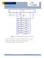
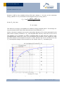
APPLICATION NOTE 309 KEYPAD USING STM 110C – A Wireless, Batteryless keypad using EnOcean STM 110C EnOcean STM 110C is extreme-low power sensor radio working at 315 MHz frequency. It can be powered by ambient energy like thermal, light etc. This application note describes how to build a wireless and batteryless multi-button keypad using STM 110C. STM 110C Operation STM 110C has three 8-bit A/D channels and four digital inputs. It is preprogrammed in factory and, once power is applied, switches itself between sleep mode and operating mode in order to save power. STM 110C can be waked up immediately from sleep mode by logic state changes on hardware pins, or periodically by a configurable timer. STM 110C always sends 4-byte data telegrams if it is waked up by the hardware pins. However, for the periodic wakeup, the microprocessor samples all analog and digital input pins after each wakeup and determines if the 4-byte data should be transmitted through the radio according to the following criteria Exception trigger + Periodic trigger Data will be transmitted if either one of the “Exception trigger” and the “Periodic trigger” becomes true. The Exception trigger becomes true if Logic state on at least one of the four digital inputs changes Sampled data from at least one of the three A/D channels has significant change (This is triggered by the exception threshold and it is configurable. Please see the STM 110C user manual) The periodic trigger becomes true periodically based on a configurable redundant transmission counter. This will define the maximum transmission period of the module. Most keypad applications require immediate action after one or more keys are pressed. So the hardware wakeup feature of STM 110C should be used for keypad interface. © EnOcean | www.enocean.com Subject to modifications | Eugene You | March 2009 | Page 1/ 8 APPLICATION NOTE 309 KEYPAD USING STM 110C Keypad Interface Variety of interface methods exists between keypad and MPU. The following few keypad interface methods with STM 110C can be considered due to the fact that the STM 110C is pre-programmed in factory and the operating mode is fixed. User cannot reprogram it. Use WAKE / WAKE and digital input pins Use WAKE / WAKE and A/D input pins Use WAKE / WAKE and combination of digital input and A/D input pins The key is that when any key is pressed down the STM 110C will be waked up and the unique information associated with the key (digital or analog or both) should be sampled by STM 110C. The information associated with the key will become part of the 4-byte data payload and will be transmitted to the remote receiver. The key decoding can be done at the receiver side. One more thing we have to keep in mind is that this is low power design. The circuit should not draw excessive current when no key is pressed. Example Picture 1 gives an example of keypad interface circuit to STM 110C. It uses the WAKE / WAKE pins for wakeup and one A/D input pin for key sensing. SOL1 and SOL2 connect to solar cells (See user manual of STM110C). V_REF is the reference voltage output of STM 110C (2.05V) which is only available during wake up (~2.6 ms). The gate of Q1 is driven high by V_SC1 through R10 when no key is pressed. Thus the STM 110C pin WAKE is high and the pin WAKE is low. When any of the keys is pressed done, the gate of Q1 will be pulled low so the STM 110C pin WAKE will be low and WAKE will be high. The change of state on the differential pins WAKE / WAKE will cause STM 110C to wake up, enable V_REF output and sample all digital and analog inputs. In this example, the analog channel AD_0 is connected to a resistor divider network. The resistance of R1 to R9 is carefully chosen so that the voltages appeared at AD_0 when different keys are pressed have the optimal spacing which will minimize the error rate at key decoding. The equivalent circuit is shown on Figure 2 if only one key is pressed each time. Vd is the equivalent forward voltage drop across a diode. V _ REF is the reference voltage (2.05V) outputted from STM 110C during wake up. © EnOcean | www.enocean.com Subject to modifications | Eugene You | March 2009 | Page 2/ 7 APPLICATION NOTE 309 KEYPAD USING STM 110C Figure 1. An example keypad circuit interface to STM 110C Rs is the input impedance of A/D channel of STM110C, which is ≥ 100 KΩ. Rk is the contact resistance of the push button switches (keys). Ri is the divider resistors R1 to R8 shown in Figure 1. © EnOcean | www.enocean.com Subject to modifications | Eugene You | March 2009 | Page 3/ 7 APPLICATION NOTE 309 KEYPAD USING STM 110C The sampled voltage when a key K i ( i = 1…8) is pressed can be calculated From figure 2 as follow: Vi = V _ REF Vd + R9 R R + Rk Ri + Rk + 9 1+ i + 1+ Ri + Rk Rs R9 Rs (1) If the resistance of the key contact can be ignored, then (1) becomes Vi = V _ REF Vd + R R R R 1+ 9 + 9 1+ i + i Ri Rs R9 Rs (2) STM110C R9 I i2 Vi Ri i1 V_REF AD_0 Vd Rs A/D Rk 2 2 Figure 2. The equivalent circuit for A/D channel Figure 3. Sampled voltage vs Resistors Assume Vd =0.5V, Rs =100KΩ and Rk =0. The plots of sampled voltage against divider resistor Ri with three different values of R9 are given in Figure 3. It is obvious that the smaller R9 results in bigger span of data range. The sampled data close to the full span of the reference voltage (2.05V) when R9 =2K in the scope of Ri ≤ 100K. R9 must be kept smaller than 10K. © EnOcean | www.enocean.com Subject to modifications | Eugene You | March 2009 | Page 4/ 7 APPLICATION NOTE 309 KEYPAD USING STM 110C Because V_REF is only available during STM 110C wakeup (~ 2.6 ms), so the maximum energy (assume Ri =0) consumed on the keypad circuit for a key push is Ek = 2.6ms V _ REF (V _ REF − Vd ) R9 If take R9 =2K, then E k =4.13μWs This amount of energy is acceptable for ambient energy powered device. The average energy consumed will be lower than this because of the resistors Ri ≠ 0 . Figure 4 shows an example how to do key decoding. Because of the noise generated by the push button contact (variation in Rk ) the sampled data and key value will not be one to one mapping. It is necessary to make a mapping table to map each key value to nonoverlapped small regions on Y axis. The red lines are the centers of such regions for each key (from bottom up correspond to keys K1 to K8). Because the curve rise fast at the low Ri , the sampled voltage is more sensitive to the resistor value Ri . Considering the Figure 4. Key value decoding © EnOcean | www.enocean.com Subject to modifications | Eugene You | March 2009 | Page 5/ 7 APPLICATION NOTE 309 KEYPAD USING STM 110C variation of the resistor values due to tolerance and the temperature variation, the voltage spacing is chosen to be wider at the low side of resistor Ri . The decoding error occurs when the sampled data falls in the regions in the neighborhood. So a guard band between two regions next to each other can help reducing decoding error. If a value falls into the guard band then it should be considered as invalid key stroke. As mentioned above, noisy key pad contact can generate noise on the sampled voltage. A simulated noisy contact with Rk varies randomly between 0 to 500 Ohms is shown in Figure 5. It is obvious that the sampled voltage is more sensitive to the contact Ohmic noise to the keys with lower Ri . This is why wider voltage spacing and voltage guard band should be allocated at the lower Ri side. Please note that the Ohmic noise Rk always shift the curve up. This implies that an asymmetric mapping region will give a better performance. Figure 5. Keypad contact noise Another very important issue is key debounce. It is standard practice to give 20ms delay when detect and read a key stroke from keypad to MPU interface to skip the noisy key debouncing period. However, STM 110C only gives 2.6 ms during wakeup. Because all analog and digital channels are sampled during this time period, so much noisier signals are expected for the keypad interface that is discussed here. © EnOcean | www.enocean.com Subject to modifications | Eugene You | March 2009 | Page 6/ 7 APPLICATION NOTE 309 KEYPAD USING STM 110C Conclusions Wireless keypad interface to the ambient energy powered EnOcean STM 110C is discussed and a simple example is given. Keypad with more keys can be constructed the same way by using more A/D channels, or by the combination of analog and digital channels. Decoding error is a very important factor for a keypad. There are many trade-offs that will affect the decoding error. User should consider the specific application and the reliability requirement when design a keypad. The following few areas should be always considered carefully for this matter Use Digital (less error) or analog interface, or combination of two How many keys are assigned to each analog channel (the less key the wider spacing and the less decoding error) How a channel is segmented through choosing the divider resistors R9 and Ri How large is the mapping regions and guard band (the wider the guard band the less the decoding error, but more invalid key strokes) Quality of the keypad contact Tolerance of the resistors used. It is also recommended for the user to measure the accurate A/D channel input impedance because user manual of STM 110C gives only the range (≥100K). Disclaimer The information provided in this document describes typical features of the EnOcean radio system and should not be misunderstood as specified operating characteristics. No liability is assumed for errors and / or omissions. We reserve the right to make changes without prior notice. For the latest documentation visit the EnOcean website at www.enocean.com. © EnOcean | www.enocean.com Subject to modifications | Eugene You | March 2009 | Page 7/ 7


![[13] Chap.11 Trouble Shooting](http://vs1.manualzilla.com/store/data/005753222_1-b84b48489eb920e39ff2c53b244a8bf5-150x150.png)