1
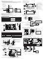
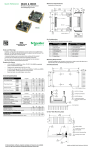
IB481H Pin Configuration
Quick Reference
IM481H Plus
Pin #
1
Ultra miniature
microstepping driver
Function
Pin #
Function
11
Power Supply Return (Ground)
Phase A Motor Connection
2
Phase A Motor Connection
12
+12 to +48 VDC Power Input
3
Current Reduction Adjust
13
Reset Input
4
Current Reference Output
14
+5 VDC Logic Supply Input
5
Current Adjustment
15
Step Clock Input
6
Fault Input
16
CW/CCW Direction Input
7
Microstep Resolution Select 0
17
Enable/Disable Input
8
Microstep Resolution Select 1
18
On-Full-Step Output
9
Microstep Resolution Select 2
19
Fault Output
10
Microstep Resolution Select 3
20
Phase B Motor Connection
21
Phase B Motor Connection
Minimum Requir ed Connections
The following illustration shows the minimum connection requirements for operating the IM481H. For use and interface of the other I/O points, please refer to the full
product manual.
Stepping Motor
IM481H
21
20
Notes and Warnings
Installation, configuration and maintenance must be carried out by qualified technicians only. You must have detailed information to be able to carry out this work. This
information can be found in the user manual.
•
Unexpected dangers may be encountered when working with this product!
•
Incorrect use may destroy this product and connected components!
The user manual is not included, but may be obtained from the Internet at:
http://www.imshome.com/downloads/manuals.html.
General Specifications
Condition
Min
Typ
Max
Unit
—
RMS
Peak
I/O Floating
I/O Floating
IOUT= 1A RMS
+12
0.14
—
—
—
—
—
—
—
1
100
2
+48
1.5
2.1
—
150
—
VDC
A
A
mA
mA
W
Condition
Min
Typ
Max
Unit
All Inputs
All Inputs Except Reset
Reset Input
MSEL 0-3, Enable
Step Clock, Direction
Reset
Fault Input
—
2
—
—
—
—
—
2
-2
—
2.3
—
—
2.3
20
2.0
1.0
4.7
—
—
0.5
—
1.2
—
—
—
—
—
—
—
—
—
—
VDC
VDC
VDC
kΩ
kΩ
kΩ
kΩ
mA
mA
VDC
VDC
Thermal Specifications
Min
Typ
Max
Unit
Storage Temperature
Operating Temperature
Rear Plate Temperature (Add't Cooling may be required)
-40
-40
—
—
—
—
+125
+85
+70
°C
°C
°C
Motion Specifications
Min
Typ
Max
Unit
—
—
—
—
2.5
16
MHz
—
Electrical Specifications
Input Voltage Range (Includes Back EMF)
Phase Output Current
Phase Output Current
Quiescent Current (+V)
Quiescent Current (+5V Input)
Active Power Dissipation
Logic Specifications
Low-Level Input Voltage
High-Level Input Voltage
High-Level Input Voltage
Input Pull-Up Resistance
Low-Level Output Current
High-Level Output Current
Low-Level Output Voltage
High-Level Output Voltage
Fault, Fullstep
IOL = 2 mA
IOH = 1.7 mA
16
15
14
13
12
11
10
9
8
7
6
5
4
2
1
Phase B
Phase B
Controller
Clock Output
CW/CCW
Step Clock
+
+5 VDC Logic Supply
22μF
10V
Motor Power
400
6400
Available Microsteps Per Revolution
800
1000
1600
2000
3200
10000
12800 25000 25600
50000
MSEL 3
MSEL 2
See
Equation A
MSEL 1
+
+
MSEL 0
0.1μF
100V
Current Adjustment Input
Current Reference Output
Current Adjust Resistor
(See Equation B)
Phase A
Phase A
Equation A: Filter Capacitor (Aluminum Electrolytic)
Amps Peak X 150μF
Example: 1.5 Amps Peak X 150μF = 200μF
Use 200μF Electrolytic Capacitor
Equation B: Calculating the Current Adjust Resistor
Example: 1.5 Amps Peak X 1000 = 1500Ω
Use 1500Ω 1% Resistor to set Peak output of 1.5A
Truth Table: Microstep Resolution Select Settings
Assumes 1.8° Stepping Motor
0 = LOW (Switch Closed), 1 = HIGH (Switch Open).
MSEL Inputs Pulled to +5V Internally using a 20kΩ Resistor
Resolution
Microsteps/Step
2
4
8
16
32
5000
51200
+12 to +48
VDC Supply
(Unregulated,
±10% Ripple)
DIP Switch
(See Truth Table)
Ground
Amps Peak X 1000
Step Clock Rate
Number of Microstep Resolutions
+5 VDC
Logic Supply
(Regulated,
±5% Ripple)
Steps/Rev
MSEL 0
MSEL 1
Binary Resolutions
400
0
800
1
1600
0
3200
1
6400
0
0
0
1
1
0
MSEL 2
MSEL 3
0
0
0
0
1
0
0
0
0
0
Mechanical Specifications
64
12800
1
0
1
0
Dimensions in Inches (mm)
128
25600
0
1
1
0
256
51200
1
1
1
0
2.700
(68.6)
0.132
(3.35)
0.538
(13.6)
Decimal Resolutions
0.175
(4.5)
2.450
(62.2)
2 X Ø 0.150
(3.8)THRU
65°
TYP.
1.100
(27.9)
5
1000
0
0
0
1
10
2000
1
0
0
1
25
5000
0
1
0
1
50
10000
1
1
0
1
125
25000
0
0
1
1
250
50000
1
0
1
1
1
1
1
1
1
1
Full Step
0.175
(4.4)
1
200
180
0.225
(5.7)
0
.01 Degrees
PIN 1
0.100
(25.4)
0.016
(0.4) SQ.
36000
1
0.058
(1.5)
All documentation, software, program examples and resources are available
online at: http://www.imshome.com/products/drivers_pcb_mounted.html.
IM481H Plus Quick Reference R020510
IM481H Mounting Requirements
H481 Heat Sink Kit
The IM481H is designed to be socketed or soldered into a PCB. For PCB layout information and circuit board hole pattern please refer to the product manual. This part of
the Quick Reference only supplies mechanical mounting information.
Heat Sink Dimensions
2.872
(72.9)
PCB Mounting
0.178
(4.5)
0.498
(12.6)
3 1 - H-481 Heat Sink
0.312
(7.9)
D 2 - 8-32 x 1.375 Scew
A 2 - 6-32 x 5/8 Screw
D
TI-481 Isolated Thermal
Pad (REQUIRED!)
G 2 - Spacers
F
IM481H Plus
A
Heat Sink Kit Contents
2.373
(60.2)
1.312
(33.3)
3
F 2 - #8 Split Washers
C 2 - #6 Flat Washers
C
B
B 2 - #6 Split Washers
2X Ø 0.177 (4.5) THRU
2.450
(62.2)
0.211
(5.4)
G
1.100
(27.9)
0.096
(2.43)
PCB
0.550
(13.9)
2X Ø #6-32
THRU
INT-481 Interface Board
Opto-Isolated Inputs
General Specifications
All test data was taken at 25˚ at an input voltage of +45 VDC.
JP1 Settings
Isolated Inputs
Fault, Full Step
+5V - Optos Powered by on-board +5V
(Sinking Inputs, Non-Isolated)
21
3
JP1
OPTO/+5V
VDC
VDC
mA
VDC
VDC
mA
VDC
Ω
1
+48
+40
15
1.7
—
20
100
—
OPTO - Optos Powered by External
+5 to +40 VDC Supply (Sinking Inputs, Isolated)
4
—
—
—
1.5
—
—
—
—
6
+12
+5
5
—
5
—
—
6.5
5
—
7
Unit
1
Max
3
Typ
2
Min
JP1
Input Voltage
Optocoupler Supply Voltage
Input Forward Current
Input Forward Voltage
Reverse Breakdown Voltage
Signal Output Current
Drain-Source Voltage
Drain-Source On Resistance (IDS = 25mA)
Condition
OPTO/+5V
Electrical Specifications
NOTE: The Internal +5 VDC is
referenced to Power Ground.
Using this supply defeats the
Optical Isolation.
+5 VDC
JP1
INT-481 Mechanical Specifications
+5 to +40 VDC Opto Supply Pin 7
Dimensions in Inches (mm)
0.920
(23.37)
3.000
(76.2)
Enable/Disable
Reset
CW/CCW Direction
Step Clock
0.620
(15.75)
2.450
(62.23)
0.275
(6.99)
Optocoupler
21
1
Pin 5
Pin 6
Pin 8
Pin 9
SW1
432 1
JP2
MS0
MS1
MS2
MS3
POWER
RED
LED1
Micr ostep Resolution
0.575
(14.6)
SW1
432 1
Heat Sink
This Side
2X Ø 0.143 (3.6) Thru.
MS0
MS1
MS2
MS3
Pin #
Function
Phase B Motor Output
8
CW/CCW Direction Input
2
Phase B Motor Output
9
Step Clock Input
3
Phase A Motor Output
10
Fault Output
4
Phase A Motor Output
11
On-Full-Step Output
5
Enable/Disable Input
12
+12 to +48 VDC Motor Power Supply
6
Reset
13
Power Supply Return (Ground)
7
Optocoupler Supply (+5 to +40 VDC)
14
Current Adjustment
15
Current Reduction
GRN
RED
LED1
A
FAULT
Function
1
MS0
MS1
MS2
MS3
B
Closed, (Logic 0)
See Table on reverse
side of this page for
MSEL Settings.
Setting shown on
diagram is 51,200
Steps/Revolution.
POWER
INT-481 Pin Configuration
B
Minimum Requir ed Connections
Disable Bridge
Following Move
Using Internal
+5VDC for Optos
Mounting
Select Desired
Resolution
21
TI-481 Isolating Thermal Pad
1
Panel or Heat Sink
SW1
(Included in H-481 Heat Sink Kit)
C
A 2 - 6-32 x 5/8 Screw
B
ENOFF/ENON
3
1
3
Hardware Required
JP2
MS0
MS1
MS2
MS3
1
B 2 - #6 Split Washers
JP1
IM481H Plus
OPTO/+5V
Pin #
Open, (Logic 1)
432 1
Pin 1
A
SW1
1
432 1
GRN
FAULT
14
15
11
13
12
8
9
10
6
7
3
4
5
1
2
1
1.550
(39.37)
JP1
OPTO/+5V
3
ENOFF/ENON
3
1
C 2 - #6 Flat Washers
Power On LED
Fault LED
Reduction Adjust Resistor (1/8 W 1% Ω) (See Equation B)
ENOFF/ENON
EQUATION A
R ADJUST
JP2
ENOFF/ENON
3
1
I PEAK
JP2
Stepping Motor
=
+
X 1000
Direction
Switch
EQUATION B
R RED
ENOFF - Current Reduction
By Resistor
13 14 15
A
Copyright © Schneider Electric Motion USA
-I
HOLD
15
13
14
12
11
9
10
8
I RUN
ENON - Outputs Disable After a
move (0 Hold Current)
DO NOT USE A REDUCTION
ADJUST RESISTOR!
= 1000
I RUN X I HOLD
B
www.schneider-electric-motion.us
X
Controller
Clock Output
-
+12 to +48
VDC Supply
(Unregulated,
±10% Ripple)
GRN
POWER
15
14
13
Ground
Current Adj.
11
12
+V
10
9
8
CW/CCW
7
5
6
4
Phase A
3
Current Adjust Resistor (1/8 W 1% Ω) (See Equation A)
Step Clock
JP2 Settings
Phase A
1
A current adjustment resistor is REQUIRED.
Phase B
Phase B
Setting Run and Hold Output Current
2
0.180
(4.57) Ref
RED
LED1
FAULT
A