1
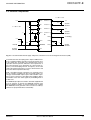
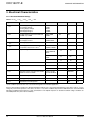
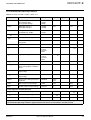
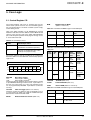
ADVANCE INFORMATION
CDC1607F-E
Automotive Controller
Specification
Edition March 31, 2003
6251-608-2AI
MICRONAS
CDC1607F-E
ADVANCE INFORMATION
Contents
Page
Section
Title
3
3
7
1.
1.1.
1.2.
Introduction
Features
Abbreviations
9
9
10
11
2.
2.1.
2.2.
2.3.
Package and Pins
Package Outline Dimensions
Pin Assignment
External Components
12
3.
Electrical Characteristics
16
4.
CPU, RAM, ROM and Banking
17
17
5.
5.1.
Core Logic
Control Register CR
19
19
6.
6.1.
Hardware Options
Functional Description
20
7.
Differences
22
8.
Data Sheet History
2
March 31, 2003; 6251-608-2AI
Micronas
Release Note: Revision bars indicate significant changes to the previous edition.
The IC is a single-chip controller for use in automotive applications. The CPU on the chip is an upgrade of the 65C02 with 16-bit internal data and 24-bit address
bus. The chip consists of timer/counters, an interrupt controller, a multichannel A/D converter, a stepper motor and LCD driver, CAN interfaces and PWM outputs.
This document provides MCM Flash hardware-specific information. General information on operating the IC can be found in the document “CDC16xxF-E Automotive Controller Family User Manual” (6251-606-2AI).
ADVANCE INFORMATION
Micronas
1. Introduction
1.1. Features
Table 1–1: CDC16xxF Family Feature List
March 31, 2003; 6251-608-2AI
This Document:
Item
CDC1605F-E
EMU
CDC1607F-E
MCM Flash
CDC1631F-E
MASK ROM
CDC1605F-C
EMU
CDC1607F-C
MCM Flash
CDC1641F-C
Mask ROM
CDC1652F-C
Mask ROM
CDC1672F-C
Mask ROM
2.75 KB
4 KB
6 KB
90 KB
128 KB
216 KB
Core
CPU
16-bit 65C816, featuring software compatibility with its 8-bit NMOS and CMOS 6500-series predecessors
CPU-Active Operation
Modes
FAST, SLOW and DEEP SLOW
FAST and SLOW
Power Saving Modes
(CPU Inactive)
WAKE and IDLE
-
EMI Reduction Mode
selectable in FAST mode
Oscillators
4 MHz to 12 MHz Quartz, RC
RAM
6 KB
ROM
ROMless,
external program storage
with up to
16 MB, internal
2 KB Boot
ROM
2 KB
6 KB
64 KB
ROMless,
external program storage
with up to
16 MB, internal
2 KB Boot
ROM
256 KB Flash,
bottom boot
configuration,
internal 2 KB
Boot ROM
3
CDC1607F-E
256 KB Flash,
bottom boot
configuration,
internal 2 KB
Boot ROM
4 MHz to 12 MHz Quartz
This Document:
March 31, 2003; 6251-608-2AI
Item
CDC1605F-E
EMU
CDC1607F-E
MCM Flash
CDC1631F-E
MASK ROM
Multiplier, 8 by 8 bit
✔
Digital Watchdog
✔
Central Clock Divider
✔
Interrupt Controller
expanding NMI
16 inputs,16 priority levels
Port Interrupts including
Slope Selection
4 inputs
Port Wake-Up Inputs
including Slope / Level
Selection
✔
Patch Module
10 ROM locations
5 ROM locations
Boot System
allows in-system downloading of
code and data into RAM via serial
link
-
CDC1605F-C
EMU
CDC1607F-C
MCM Flash
CDC1641F-C
Mask ROM
CDC1652F-C
Mask ROM
10 ROM locations
5 ROM locations
6 ROM locations
allows in-system downloading of
code and data into RAM via serial
link
-
-
CDC1672F-C
Mask ROM
-
CDC1607F-E
4
Table 1–1: CDC16xxF Family Feature List, continued
-
-
Analog
Combined Input for Regulator Input Supervision
Clock and Supply
Supervision
✔
10-bit ADC, charge
balance type
9 channels (5 channels selectable as digital input)
ADC Reference
VREF Pin
Comparators
P06COMP with 1/2 AVDD reference
LCD
Internal processing of all analog voltages for the LCD driver
Micronas
ADVANCE INFORMATION
Reset/Alarm
This Document:
Item
CDC1605F-E
EMU
CDC1607F-E
MCM Flash
CDC1631F-E
MASK ROM
CDC1605F-C
EMU
CDC1607F-C
MCM Flash
CDC1641F-C
Mask ROM
CDC1652F-C
Mask ROM
CDC1672F-C
Mask ROM
Communication
March 31, 2003; 6251-608-2AI
DMA
1 DMA Channel for serving the
Graphics Bus interface
-
1 DMA Channel for serving the
Graphics Bus interface
-
1 DMA Channel for serving the
Graphics Bus interface
UART
3: UART0, UART1 and UART2
1: UART0
3: UART0, UART1 and UART2
1: UART0
3: UART0, UART1 and UART2
Synchronous Serial
Peripheral Interfaces
2: SPI0 and SPI1
1: SPI0
2: SPI0 and SPI1
1: SPI0
2: SPI0 and SPI1
Full CAN modules V2.0B
3: CAN0, CAN1 and CAN2 with
256-byte object RAM each
(LCAN000F)
1: CAN0 with
256-byte object
RAM
(LCAN000F)
3: CAN0, CAN1 and CAN2 with
256-byte object RAM each
(LCAN0009)
1: CAN0 with
256-byte object
RAM
(LCAN0009)
2: CAN0 and CAN1 with 256-byte
object RAM each (LCAN0009)
DIGITbus
1 master module
-
1 master module
-
1 master module
5 Modules: PWM0, PWM1,
PWM2, PWM3 and PWM4
2 Modules:
PWM0, PWM1
5 Modules: PWM0, PWM1,
PWM2, PWM3 and PWM4
ADVANCE INFORMATION
Micronas
Table 1–1: CDC16xxF Family Feature List, continued
Input & Output
up to 52 I/O or 48 LCD segment lines (=192 segments),
in groups of two, configurable as I/O or LCD
Universal Port Slew Rate
HW preselectable
Stepper Motor Control
Modules with High-Current Ports
5 Modules, 24 dI/dt controlled ports
8-bit PWM Modules
5 Modules: PWM0, PWM1,
PWM2, PWM3 and PWM4
Audio Module with autodecay
✔
SW selectable Clock outputs
2
3 Modules:
PWM0, PWM1,
PWM2
5
CDC1607F-E
Universal Ports selectable as 4:1 mux LCD
Segment/Backplane lines
or Digital I/O Ports
This Document:
Item
CDC1605F-E
EMU
CDC1607F-E
MCM Flash
CDC1631F-E
MASK ROM
Polling / Flash Timer Output
1 High-Current Port output operable in Power Saving
Mode
CDC1605F-C
EMU
CDC1607F-C
MCM Flash
-
CDC1641F-C
Mask ROM
CDC1652F-C
Mask ROM
CDC1672F-C
Mask ROM
CDC1607F-E
6
Table 1–1: CDC16xxF Family Feature List, continued
Timers & Counters
March 31, 2003; 6251-608-2AI
16-bit free running
counters with Capture/
Compare modules
CCC0 with 3CAPCOM
16-bit timers
1: T0
8-bit timers
2: T1 and T2
Real Time Clock, Delivering Hours, Minutes and
Seconds
✔
-
Miscellaneous
✔
-
Various randomly selectable HW options
Most options SW programmable,
copy from user program storage
during system start-up
Core Bond-Out
✔
Supply Voltage
4.5 V to 5.5 V
Temperature Range
Tcase: −40 to +105C
Tamb: −40 to +85C
Type
Ceramic
177PGA
Plastic 100QFP
0.65mm pitch
Ceramic
177PGA
Plastic 100QFP
0.65mm pitch
Bonded Pins
176
100
176
100
-
-
✔
Scalable layout in CAN,
RAM and ROM
Mask programmed
according to
user specification
Most options SW programmable,
copy from user program storage
during system start-up
✔
-
Micronas
ADVANCE INFORMATION
Package
March 31, 2003; 6251-608-2AI
AM
CAN
CAPCOM
CPU
DMA
ERM
IR
LCD
P06COMP
PINT
PSM
PWM
RTC
SM
SPI
T0
T1, T2
UART
Audio Module
Controller Area Network Module
Capture/Compare Module
Central Processing Unit
Direct Memory Access Module
EMI Reduction Module
Interrupt Controller
Liquid Crystal Display Module
P0.6 Alarm Comparator
Port Interrupt Module
Power Saving Module
8-Bit Pulse Width Modulator Module
Real-time Clock
Stepper Motor Control Module
Serial Synchronous Peripheral Interface
16-Bit Timer 0
8-Bit Timers 1 and 2
Universal Asynchronous Receiver Transmitter
ADVANCE INFORMATION
Micronas
1.2. Abbreviations
CDC1607F-E
7
CDC1607F-E
ADVANCE INFORMATION
VSS
VDD
UVDD
UVSS
CAN 1 *
UPort1
LCD Control
8
Test
Patch Module
RESETQ
TEST
Watchdog
Clock
DMA Logic
UPort2
Reset/Alarm
8
Banking
8-Bit Timer 1
ERM
RC Oscillator
65C816
CPU
16-Bit
CAPCOM 1
RTC
Power Saving
Module
8-Bit Timer 2
16 Inputs
Interrupt
Controller
16-Bit
CAPCOM 2
16-Bit Timer 0
8
UPort3
XTAL1
XTAL2
DIGITbus
Audio Module
6k RAM *
Multiplier
8 by 8 bit
UART 0
9
PPort0
UART 2
10-Bit ADC
CAN 2 *
8
UPort4
VREF
AVDD
AVSS
8
8-Bit PWM 0
CAN 0 *
SPI 0
8-Bit PWM 4
UPort6
HPort2
16-Bit
CAPCOM 0
UART 1
8-Bit PWM 2
Boot ROM
6
Clock Out 1
UPort5
ROMless
or
256kFlash *
8
UPort7
6
HPort1
6
HPort0
Clock Out 0
Stepper Motor
Control
4
6
HPort3
SPI 1
HVDD1
HVSS1
HVDD2
HVSS2
8-Bit PWM 1
8-Bit PWM 3
* Scalable within wide limits
Fig. 1–1: Block diagram of CDC1605F-E/CDC1607F-E
8
March 31, 2003; 6251-608-2AI
Micronas
CDC1607F-E
ADVANCE INFORMATION
2. Package and Pins
2.1. Package Outline Dimensions
29 x 0.65 = 18.85
0.65
0.17
80
51
14
17.2
8
1.8
10
9.8
5
16
100
1
19 x 0.65 = 12.35
8
1.8
0.65
50
0.37
81
31
30
2.70
23.2
3.0
0.1
20
SPGS0025-2(P100)/1E
Fig. 2–1: PQFP100 Plastic Quad Flat Pack 100-Pin (Weight approx. 1.61 g)
Micronas
March 31, 2003; 6251-608-2AI
9
CDC1607F-E
ADVANCE INFORMATION
2.2. Pin Assignment
Bus
Mode
ADB7
ADB6
ADB5
ADB4
ADB3
ADB2
ADB1
ADB0
LCD
Mode
SEG7.3
SEG7.2
SEG7.1
SEG7.0
SEG3.7
T2-OUT
SEG3.6
CC1-OUT
SEG3.5 SPI1-CLK-OUT
SEG3.4
T0-OUT
SEG3.3
CC2-OUT
SEG3.2
DIGIT-OUT
SEG3.1
CO1
SEG3.0 SPI1-D-OUT
SEG6.7
CAN0-TX
SEG6.6
PINT1-OUT
SEG6.5
T1-OUT
SEG6.4 SPI0-D-OUT
SEG6.3
SEG6.2
SEG6.1
SEG6.0
WEQ
SEG1.7
CEQ
SEG1.6
ITSTOUT SEG1.5
RWQ
SEG1.4
PH2
BP3
OEQ
BP2
BE
BP1
RDY
BP0
STOPCLK
VPQ
VPA
VDA
DB7
DB6
DB5
DB4
DB3
DB2
DB1
DB0
Pin Functions
Port
Port
Special Out
Special In
GWRQ
GRDQ
SPI0-CLK-OUT
T1-OUT
LCD-CLK-OUT
LCD-SYNC-OUT
CAN1-TX
SPI1-CLK-IN
WP0
DIGIT-IN
SPI1-D-IN
MULTI-TEST-IN
CAN0-RX/WP1
SPI0-D-IN
SPI0-CLK-IN
PINT2-IN/WP5
PINT1-IN/WP4
PINT0-IN/WP3
CAN1-RX/WP2
LCD-CLK-OUT
LCD-SYNC-OUT
ITSTOUT
SMB1+
SMB1SMB2+
SMB2SME1+/PWM2
SME1-/PWM0
SME2+
SME2SMA1+
SMA1SMA2+
SMA2-
SMB-COMP
SME-COMP
SMA-COMP
Basic
Function
U7.3
U7.2
U7.1
U7.0
UVSS
UVDD
U3.7
U3.6
U3.5
U3.4
U3.3
U3.2
U3.1
U3.0
U6.7
U6.6
U6.5
U6.4
TEST
RESETQ
XTAL2
XTAL1
VSS
VDD
U6.3
U6.2
U6.1
U6.0
U1.7
U1.6
U1.5
U1.4
U1.3
U1.2
U1.1
U1.0
H1.5
H1.4
H1.3
H1.2
H1.1
H1.0
HVDD1
HVSS1
H0.5
H0.4
H0.3
H0.2
H0.1
H0.0
Pin
No.
Pin
No.
91
92
93
94
95
96
97
98
99
100
1
2
3
4
5
6
7
8
9
10
11
12
13
14
15
16
17
18
19
20
21
22
23
24
25
26
27
28
29
30
31
32
33
34
35
36
37
38
39
40
90
89
88
87
86
85
84
83
82
81
80
79
78
77
76
75
74
73
72
71
70
69
68
67
66
65
64
63
62
61
60
59
58
57
56
55
54
53
52
51
50
49
48
47
46
45
44
43
42
41
100
91 90
81
1
80
30
51
31
40 41
50
NC = not connected,
leave vacant
Basic
Function
U4.0
U4.1
U4.2
U4.3
U4.4
U4.5
U4.6
U4.7
U5.0
U5.1
U5.2
U5.3
U5.4
U5.5
U5.6
U5.7
U2.0/GD0
U2.1/GD1
U2.2/GD2
U2.3/GD3
U2.4/GD4
U2.5/GD5
U2.6/GD6
U2.7/GD7
AVSS
AVDD
VREF
P0.1
P0.2
P0.3
P0.4
P0.5
P0.6
P0.7
P0.8
P0.9
H2.0
H2.1
H2.2
H2.3
H2.4
H2.5/Pol
HVSS2
HVDD2
H3.0
H3.1
H3.2
H3.3
H3.4
H3.5
Pin Functions
Port
Port
Special In
Special Out
CAN2-RX/WP7
CAN2-TX
UART2-RX
UART2-TX
UART0-RX/WP8
UART0-TX
CC2-IN
CC1-OUT
CC1-IN
CC0-IN
CO1
INT-TEST-IN
CC0-OUT
LCD-CLK-IN
AM-PWM
LCD-SYNC-IN
AM-OUT
IRQ
UART1-TX
ABORTQ
CO0
PINT3/WP6
PWM2
PINT3/UART1-RX
PINT0-OUT
LCD
Mode
SEG4.0
SEG4.1
SEG4.2
SEG4.3
SEG4.4
SEG4.5
SEG4.6
SEG4.7
SEG5.0
SEG5.1
SEG5.2
SEG5.3
SEG5.4
SEG5.5
SEG5.6
SEG5.7
SEG2.0
SEG2.1
SEG2.2
SEG2.3
SEG2.4
SEG2.5
SEG2.6
SEG2.7
Bus
Mode
ADB8
ADB9
ADB10
ADB11
ADB12
ADB13
ADB14
ADB15
ADB16
ADB17
ADB18
ADB19
ADB20
ADB21
ADB22
ADB23
P0.1 digital input
P0.2 digital input
P0.3 digital input
P0.4 digital input
P0.5 digital input
P0.6 Compar. inp.
SMC-COMP
WP9
SMD-COMP
SMC2SMC2+
SMC1SMC1+
PWM0
PWM4
PWM1
PWM3
SMD2SMD2+
SMD1SMD1+
Fig. 2–2: Pin Assignment for PQFP100 Package
10
March 31, 2003; 6251-608-2AI
Micronas
CDC1607F-E
ADVANCE INFORMATION
2.3. External Components
C = 100 n to 150 n
+5 V
UVDD
EVDD 0 to 1
+5 V
2*C
L
C = 100 n to 150 n
VDD
EVSS 0 to 1
VSS
HVDD 0 to 1
System
Ground
C
+5 V
2*C
18 p
XTAL1
C
System
Ground
HVSS 0 to 1
IC
+5 V Analog
AVDD
+5 V
18 p
XTAL2
4.7 k
VREF
10 n
47 n
Resetq
System
Ground
RESETQ
AVSS
C
Analog
Ground
UVSS
Fig. 2–3: Recommended external supply and quartz connection for low electromagnetic interference (EMI)
To provide effective decoupling and to improve EMC behavior, the small decoupling capacitors must be located as close
to the supply pins as possible. The self-inductance of these
capacitors and the parasitic inductance and capacitance of
the interconnecting traces determine the self-resonant frequency of the decoupling network. A frequency too low will
reduce decoupling effectiveness, increase RF emissions and
may affect device operation adversely.
XTAL1 and XTAL2 quartz connections are especially sensitive to capacitive coupling from other PC board signals. It is
strongly recommended to place quartz and oscillation capacitors as close to the pins as possible and to shield the XTAL1
and XTAL2 traces from other signals by embedding them in
a VSS trace.
The RESETQ pin adjacent to XTAL2 should be supplied with
a 47 nF capacitor, to prevent fast RESETQ transients from
being coupled into XTAL2, to prevent XTAL2 from coupling
into RESETQ, and to guarantee a time constant of ≥ 200 µs,
sufficient for proper Wake Reset functionality.
Micronas
March 31, 2003; 6251-608-2AI
11
CDC1607F-E
ADVANCE INFORMATION
3. Electrical Characteristics
3.0.1. Absolute Maximum Ratings
Table 3–1: UVSS = HVSS1 = HVSS2 = AVSS = 0 V
1)
Symbol
Parameter
Pin Name
Min.
Max.
Unit
VSUP
Core Supply Voltage
Port Supply Voltage
Analog Supply Voltage
SM Supply Voltage 1
SM Supply Voltage 2
VDD
UVDD
AVDD
HVDD1
HVDD2
−0.3
6.0
V
∆VDD
Voltage Difference between VDD and
AVDD, resp. UVDD
VDD, AVDD
UVDD
−0.5
0.5
V
ISUP
Core Supply Current
Port Supply Current
VDD, VSS
UVDD, UVSS
−100
100
mA
IASUP
Analog Supply Current
AVDD, AVSS
−20
20
mA
IHSUP
SM Supply Current
@Tj=105C, Duty Factor = 0.71 1)
HVDD1, HVSS1
HVDD2, HVSS2
−380
380
mA
Vin
Input Voltage
U-Ports,
XTAL,RESETQ,
TEST
UVSS−0.5
UVDD+0.7
V
P0-Ports
VREF
UVSS−0.5
AVDD+0.7
V
H-Ports
HVSS−0.5
HVDD+0.7
V
Iin
Input Current
all Inputs
0
2
mA
Io
Output Current
U-Ports
−5
5
mA
H-Ports
−60
60
mA
indefinite
s
toshsl
Duration of Short Circuit in Port SLOW
Mode to UVSS or UVDD
U-Ports except
U3.2 in DP Mode
Tj
Junction Temperature under Bias
−45
115
°C
Ts
Storage Temperature
−45
125
°C
Pmax
Maximum Power Dissipation
0.8
W
This condition represents the worst case load with regard to the intended application
Stresses beyond those listed in the “Absolute Maximum Ratings” may cause permanent damage to the device. This is a stress
rating only. Functional operation of the device at these or any other conditions beyond those indicated in the “Recommended
Operating Conditions/Characteristics” of this specification is not implied. Exposure to absolute maximum ratings conditions for
extended periods may affect device reliability.
12
March 31, 2003; 6251-608-2AI
Micronas
CDC1607F-E
ADVANCE INFORMATION
3.0.2. Recommended Operating Conditions
Table 3–2: UVSS = HVSS1= HVSS2 = AVSS = 0 V
Symbol
Parameter
Pin Name
Min.
Typ 1)
Max.
Unit
VDD
Supply Voltage
Port Supply Voltage
Analog Supply Voltage
VDD
UVDD
AVDD
4.5
5
5.5
V
HVDD
SM Supply Voltage 1
SM Supply Voltage 2
HVDD1
HVDD2
4.75
5
5.25
V
∆VDD
Voltage Difference between VDD
and AVDD resp. UVDD
VDD, AVDD
UVDD
−0.2
0.2
V
dAVDD
AVDD Ripple, Peak to Peak
AVDD
200
mV
fXTAL
XTAL Clock Frequency
XTAL1
4
12
MHz
XTAL Clock Frequency
using ERM
XTAL1
4
10
MHz
−40
110
C
0.51*VDD
V
Tj
Junction Temperature
Vil
Low Input Voltage
U-Ports
H-Ports
P0-Ports
TEST
Vih
High Input Voltage
U-Ports
H-Ports
P0-Ports
TEST
RVil
Reset Active Input Voltage
RESETQ
0.9
V
WRVil
Reset Active Input Voltage during
Power Saving Modes and Wake
Reset
RESETQ
0.6
V
RVim
Reset Inactive and Alarm Active
Input Voltage
RESETQ
1.6
2.1
V
RVih
Reset Inactive and Alarm Inactive
Input Voltage
RESETQ
2.9
V
WRVih
Reset Inactive during Power Saving Modes
RESETQ
UVDD 0.4V
V
VREFi
ADC Reference Input Voltage
VREF
2.56
AVDD
V
P0Vi
P0 ADC Input Port Input Voltage
P0-Ports
0
VREFi
V
0.2*VDD
V
V
0.86*VDD
Clock Input from External Generator
XVil
Clock Input Low Voltage
XTAL1
XVih
Clock Input High Voltage
XTAL1
0.8*VDD
DXTAL
Clock Input High-to-Low Ratio
XTAL1
0.45
V
0.55
1)
Typical values describe typical behavior at room temperature (25 °C, unless otherwise noted), with typical
Recommended Operating Conditions applied (derived from device characterization, not 100% tested).
Micronas
March 31, 2003; 6251-608-2AI
13
CDC1607F-E
ADVANCE INFORMATION
3.0.3. Characteristics differing from Characteristics described in document “CDC16xxF-E Automotive Controller Family User Manual”
Table 3–3: UVSS = HVSS1 = HVSS2 = AVSS = 0 V, 4.5 V < VDD = AVDD = UVDD < 5.5 V,
4.75 V < HVDD1 = HVDD2 < 5.25 V, TCASE = −40 °C to +105 °C, fXTAL = 10 MHz
Symbol
Parameter
Pin Name
Min.
Typ 1)
Max.
Unit
Test Conditions
Package
Rthjc
Thermal Resistance from
Junction to Case
25
C/W
Rthja
Thermal Resistance from
Junction to Ambient
60
C/W
Supply Currents
IDDF
VDD FAST Mode Supply
Current
CMOS levels on all
Inputs,
no Loads on Outputs,
difference between any
two VDDs within ±0.2 V
VDD
60
mA
Flash Write/Erase 6)
80
IDDS
VDD SLOW Mode Supply
Current
VDD
1.8
IDDD
VDD DEEP SLOW Mode
Supply Current
VDD
1.5
IDDI
VDD IDLE Mode Supply
Current
VDD
Flash Read 6)
mA
all Modules OFF 2), 6)
all Modules OFF 2), 6)
50
75
µA
fxtal = 4 MHz 6)
60
90
µA
fxtal = 10 MHz 6)
70
100
µA
internal RC oscill.
30
50
µA
0.3
mA
no Output Activity,
LCD Module ON
0.2
0.4
mA
ADC ON, ERM OFF
1
2
mA
ERM ON, fXTAL=8.4MHz
AVDD
1
10
µA
ADC and ERM OFF
UIDDq
UVDD
1
10
µA
no Output Activity,
LCD Module OFF
EIDDq
EVDD1
EVDD2
1
10
µA
no Output Activity, LCD
Module OFF
HIDDq
Sum of all
HVDD1
HVDD2
1
20
µA
no Output Activity,
SM Module OFF
IDDW
VDD WAKE Mode Supply
Current
VDD
UIDDa
UVDD Active Supply Current
UVDD
AIDDa
AVDD Active Supply Current
AVDD
AIDDq
Quiescent Supply Current
1)
Typical values describe typical behavior at room temperature (25 °C, unless otherwise noted), with typical
Recommended Operating Conditions applied (derived from device characterization, not 100% tested).
2)
Value may be exceeded with unusual Hardware Option setting
3)
Design value only, the actually observable hysteresis may be lower due to system activity and related
4)
When the ERM is active, this time value is increased by 0.121/fXTAL, e.g. 15.125 ns at 8 MHz.
5)
When the ERM is active, this time value is decreased by 0.121/fXTAL, e.g. 15.125 ns at 8 MHz.
6)
supply noise
Measured with external clock. Add 170 µA at 4 MHz, 200 µA at 10 MHz for operation on typical quartz with SR3.XTAL = 0
(Oscillator RUN mode).
14
March 31, 2003; 6251-608-2AI
Micronas
CDC1607F-E
ADVANCE INFORMATION
3.0.4. Recommended Crystal Characteristics
Table 3–4: UVSS = HVSS1 = HVSS2 = AVSS = 0 V, 4.5 V < VDD = AVDD = UVDD < 5.5 V,
4.75 V < HVDD1 = HVDD2 < 5.25 V, TCASE = −40 °C to +105 °C
Symbol
Parameter
Min.
fP
Parallel Resonance Frequency
@ CL = 12 pF
4
R1
Series Resonance Res. for
50 ms Oscillation Start-Up time
@CL= 12 pF
@ fP = 4 MHz
CEXT
Micronas
Max.
Unit
12
MHz
380
320
Ohm
START-UP
RUN
@ fP = 6 MHz
230
160
Ohm
START-UP
RUN
@ fP = 8 MHz
150
95
Ohm
START-UP
RUN
@ fP = 10 MHz
100
60
Ohm
START-UP
RUN
External Oscillation Capacitances for CL = 12 pF,
connected to VSS
Typ.
18
March 31, 2003; 6251-608-2AI
Test Conditions
pF
15
CDC1607F-E
ADVANCE INFORMATION
4. CPU, RAM, ROM and Banking
MCM
PQFP100
phys.addr.
Alternative
Bottom Boot Config.
000000
Native
log.addr.
log.addr.
0000
000000
6K RAM
001800
Reserved
001900
CAN2-RAM
001A00
CAN1-RAM
001B00
CAN0-RAM
001C00
CAN-Regs
001D00
Ext. I/O
001E00
I/O-Reg1
001F00
I/O-Reg0
002000
Sector 0,
upper 8 KB
004000
Sector 1,
8 KB
006000
Sector 2,
8 KB
008000
Sector 3,
32 KB
Bank 0
Bank 0
7FFF
8000
F800
Boot ROM
010000
018000
020000
Bank 1
Boot ROM
Sector 4,
64 KB
256 KB
Flash
EEPROM
FFFF
8000
The device contains a 256 KB Flash
EEPROM of the AMD Am29F200BT type
(bottom boot configuration). This device exhibits
electrical byte program and sector erase
functions. Refer to the AMD data sheet for
details.
010000
Bank 2
FFFF
8000
Bank 1
Bank 3
FFFF
8000
Sector 5,
64 KB
00FFFF
01FFFF
020000
Bank 4
FFFF
8000
028000
Bank 2
Bank 5
030000
FFFF
8000
Sector 6,
64 KB
02FFFF
030000
Bank 6
FFFF
8000
038000
Bank 3
Bank 7
040000
FFFF
8000
Sector 0,
lower 8 KB
Bank 8
9FFF
03FFFF
040000
Bank 4
041FFF
042000
mirrored
Flash
EEPROM
FFFFFF
Fig. 4–1: Address Map
16
March 31, 2003; 6251-608-2AI
Micronas
CDC1607F-E
ADVANCE INFORMATION
5. Core Logic
5.1. Control Register CR
The Control Register CR serves to configure the ways by
which certain system resources are accessed during operation. The main purpose is to obtain a variable system configuration during IC test.
Upon each HIGH transition on the RESETQ pin, internal
hardware reads data from the address location 00FFF3h and
stores it to the CR. The state of the TEST and ESTOPCLK
pins at this timepoint specifies which program storage source
is accessed for this read:
MFM
Multifunction Pin Mode
(Tables 5–2 and 5–3)
Table 5–2: TSTTOG and MFM usage in mask ROM parts
TSTTOG
MFM
TEST pin
Multifunction
Pins
0
0
x
Bus mode
1
0
0
Bus mode
1
normal mode
x
normal mode
Table 5–1: Control byte source
TEST
Control byte source
0 or NC
internal BOOT ROM
(standard for stand-alone operation)
x
1
external, via multifunction pins in Bus
mode (for test purposes only)
The system will thus start up according to the configuration
defined in address location 00FFF3h, automatically copied to
register CR.
CR
Control Register
7
6
r/w RESLNG TSTTOG
5
4
x
MFM
r/w RESLNG TSTTOG EBTRI
MFM
3
2
TSTROM IROM
FLASH
IROM
1
1
Table 5–3: TSTTOG, EBTRI and MFM usage in Flash and
EMU parts
TSTTOG
EBT
RI
MFM
TEST
pin
Multifunction
Pins
Emulator Bus
Pins
0
x
0
x
Bus
mode
Flash
mode
1
x
0
0
Bus
mode
Flash
mode
1
normal
mode
x
normal
mode
0
IRAM
ICPU
ROM
IRAM
ICPU
Emu
x
Value of 00FFF3h
0
1
Res
1
RESLNG
Reset Pulse Length
r/w1:
Pulse length is 4095/FXTAL
r/w0:
Pulse length is 16/FXTAL
This bit specifies the length of the reset pulse which is output
at pin RESETQ following an internal reset. If pin TEST is 1
the first reset after power on is short. The following resets
are as programmed by RESLNG. If pin TEST is 0, all resets
are long.
TSTTOG
TEST Pin Toggle (Tables 5–2 and 5–3)
This bit is used for test purposes only. If TSTTOG is true in
IC active mode, pin TEST can toggle the multifunction pins
between Bus mode and normal mode.
EBTRI
Emulator Data Bus Tristate (Table 5–3)
Flash
mode
TSTROM
TestROM (Table 5–4)
FLASH
FLASH EEPROM (Table 5–5)
IROM
Internal ROM (Tables 5–4 and 5–5)
Table 5–4: TSTROM and IROM usage in mask ROM parts
TSTROM
IROM
selected program storage
1
1
internal ROM
0
x
Micronas
Emulator mode
March 31, 2003; 6251-608-2AI
internal TestROM
0
external via Multifunction pins
in Bus mode
17
CDC1607F-E
ADVANCE INFORMATION
Table 5–5: FLASH and IROM usage in FLASH and EMU
parts
FLASH
IROM
selected program storage
1
1
internal FLASH EEPROM
resp. Emulator Bus
0
internal BOOT ROM
x
0
external via Multifunction pins
in Bus mode
IRAM
r/w1:
r/w0:
Internal RAM
Enable internal RAM.
Disable internal RAM.
ICPU
r/w1:
r/w0:
Internal CPU
Enable internal CPU.
Disable internal CPU.
Table 5–6: Some commonly used settings for address
location 00FFF3h. A copy is automatically transferred to the
CR during IC start-up.
Code
TEST
Pin
Operation Mode
FFh
0
Stand-alone with internal ROM or Flash
ABh
1
External program storage connected to
multifunction pins in Bus mode
DFh
0
Emulator mode (CPGA177 package)
18
March 31, 2003; 6251-608-2AI
Micronas
CDC1607F-E
ADVANCE INFORMATION
6. Hardware Options
6.1. Functional Description
Hardware Options are available in several areas to
adapt the IC function to the host system requirements:
– clock signal selection for most of the peripheral
modules from fosc to fosc/217 plus some internal signals. (see table in Chapter Hardware Options of
document “CDC16xxF-E Automotive Controller
Family User Manual”.)
– interrupt source selection for interrupt inputs 5, 6, 7,
13, 14 and 15
– Special Out signal selection for some U and H-ports
– Rx/Tx polarity selection for SPI and UART modules
– U-port Port Slow Mode selection
Hardware Option setting requires two steps:
1. selection is done by programming dedicated
address locations with the desired options’ code
2. activation is done by a read access to these dedicated address locations at least once after each reset.
Address locations 00FFB8h through 00FFBFh do not
allow random setting. Their respective Hardware
Options are hard-wired and can only be altered by
changing a production mask for this IC. By default, the
Port Slow Option is set for all U-Ports, with the exception of U1.0 to U1.3 (Port Fast Option is set). The
Watchdog and Clock Monitor are activated via software by default.
Future mask ROM derivatives of this IC will not require
(but will tolerate) activation of option settings by read
accesses, as the ROM as well as the options will be
hard-wired. Instead, the manufacturer will automatically process the setting of the dedicated address
locations, as given in the ROM code file, to set the
required mask changes.
To ensure compatible option settings in this IC and
mask ROM derivatives when run with the same ROM
code, it is recommended to always read locations
00FFA0h through 00FFC3h directly after reset. Please
note that the non-programmable locations 00FFB8h
through 00FFBFh may not be compatible within this IC
and the mask ROM derivative.
Micronas
March 31, 2003; 6251-608-2AI
19
CDC1607F-E
ADVANCE INFORMATION
7. Differences
This chapter describes differences of this document to predecessor document “CDC1607F-E Automotive Controller
Specification”, Feb. 17, 2003, 6251-606-1AI.
#
Section
1
Introduction
Description
Table 1–1: "CDC16xxF Family Feature List" on page 3:
Name and features of “Example E-Family” changed into “CDC1631F-E”,
Multiplier, 8 by 8 bit added.
Fig. 1–1: “Block diagram of CDC1605F-E/CDC1607F-E” on page 8:
Multiplier, 8 by 8 bit added
2
External Components
3
Core Logic
Value of C at RESETQ changed from 47 µ to 47 n, value of C at VREF changed from 10 µ to 10 n and
text added.
Table 5–1: "Control byte source" on page 17:
Updated / minimized
4
5
20
CPU, RAM, ROM and Banking
Fig. 4–1: “Address Map” on page 16:
Differences
New Chapter
Layout format corrected.
March 31, 2003; 6251-608-2AI
Micronas
CDC1607F-E
ADVANCE INFORMATION
Micronas
March 31, 2003; 6251-608-2AI
21
CDC1607F-E
ADVANCE INFORMATION
8. Data Sheet History
1. Advance Information: “CDC1607F-E Automotive Controller Specification”, Feb. 17, 2003, 6251-608-1AI. First release
of the advance information. Originally created for the HW
version CDC1607F-E1.
2. Advance Information: “CDC1607F-E Automotive Controller Specification”, March 31, 2003, 6251-608-2AI. Second
release of the advance information. Originally created for the
HW version CDC1607F-E2.
Micronas GmbH
Hans-Bunte-Strasse 19
D-79108 Freiburg (Germany)
P.O. Box 840
D-79008 Freiburg (Germany)
Tel. +49-761-517-0
Fax +49-761-517-2174
E-mail: [email protected]
Internet: www.micronas.com
Printed in Germany
Order No. 6251-608-2AI
22
All information and data contained in this data sheet are without any
commitment, are not to be considered as an offer for conclusion of a
contract, nor shall they be construed as to create any liability. Any new
issue of this data sheet invalidates previous issues. Product availability
and delivery are exclusively subject to our respective order confirmation
form; the same applies to orders based on development samples delivered. By this publication, Micronas GmbH does not assume responsibility for patent infringements or other rights of third parties which may
result from its use.
Further, Micronas GmbH reserves the right to revise this publication and
to make changes to its content, at any time, without obligation to notify
any person or entity of such revisions or changes.
No part of this publication may be reproduced, photocopied, stored on a
retrieval system, or transmitted without the express written consent of
Micronas GmbH.
March 31, 2003; 6251-608-2AI
Micronas