1
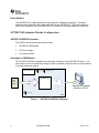
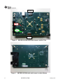
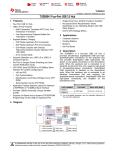
www.ti.com SLLU143A – October 2010 - Revised January 2011 SN75DP130 EVM User’s Manual High Performance Analog / Interface Group ABSTRACT The SN75DP130 is a single port Dual-Mode DisplayPort (DP++) repeater that regenerates the DP high speed digital link. The device complies with the VESA Embedded DisplayPort Standard Version 1.2 supporting up to four lanes of 5.4 Gbps (HBR2) and DP++ dual-mode TMDS signaling for full HDMI 1.4a data rate support. The device compensates for PCB related frequency loss and switching related loss to provide the optimum DP electrical performance from source to sink. The Main Link signal inputs feature configurable equalizers with selectable boost settings. At the Main Link output, four primary levels of differential output voltage swing (VOD) and four primary levels of pre-emphasis are available, as well as a secondary level of boost adjustment, programmed through I2C, for fine-tuning the Main Link output. The device can monitor the AUX channel and automatically adjust the output signaling levels and input equalizers in response to Link Training commands. Additionally, the SN75DP130 output signal conditioning and EQ parameters are fully programmable through the I2C interface. The SN75DP130 offers separate AUX and DDC source ports and an AUX sink port. This minimizes component count when implemented with a graphics processor (GPU) comprising separate DDC and AUX interfaces. For GPUs with combined DDC/AUX, the device can operate as a FET switch to short circuit the AUX channel AC coupling caps while connected to a TMDS sink device. Other sideband circuits such as Hot Plug Detect (HPD) are optimized to reduce external components, providing a seamless connection to Intel, AMD, and NVIDIA graphics processors. The SN75DP130 is optimized for mobile applications, and contains activity detection circuitry on the Main Link input that transitions to a low-power Output Disable mode in the absence of a valid input signal. Other low power modes are supported, including a Standby mode with typical dissipation of ~2mW when no video sink (eg. monitor) is connected. The device is characterized for an extended operational temperature range from 0ºC to 85ºC. 1 SN75DP130 EVM January 2011 Contents Introduction .............................................................................................................................................3 SN75DP130 Evaluation Module Configuration.....................................................................................3 SN75DP130 EVM Kit Contents.........................................................................................................3 Description of EVM Board.................................................................................................................3 PCB Construction ...................................................................................................................................6 SN75DP130 EVM Board Layout .......................................................................................................6 SN75DP130 EVM Board Construction..............................................................................................9 SN75DP130 EVM Material Listing ..................................................................................................10 SN75DP130 EVM Board Schematics .............................................................................................10 Appendix A – Bill of Materials..............................................................................................................11 Figure 1. Figure 2. Figure 3. Figure 4. Figure 5. Figure 6. Figure 7. Figure 8. Figure 9. Figure 10. Figures SN75DP130 EVM Block Diagram ........................................................................................3 SN75DP130 EVM Switch and Jumper Location (Top).........................................................4 SN75DP130 EVM Switch and Jumper Location (Botom).....................................................4 SN75DP130 EVM Top Layer 1 ............................................................................................6 SN75DP130 EVM Ground Layer 2.......................................................................................7 SN75DP130 EVM Power Layer 3 ........................................................................................7 SN75DP130 EVM Power Layer 4 .......................................................................................8 SN75DP130 EVM Ground Layer 5.......................................................................................8 SN75DP130 EVM Bottom Layer 6 (Mirrored) ......................................................................9 EVM Layer Stack-up ............................................................................................................9 Table 1. Table 2. Tables Jumper and Switch Functionality..........................................................................................5 DP130 EVM Bill of Materials ..............................................................................................11 2 SN75DP130 EVM January 2011 Introduction The SN75DP130 is a high-speed one-to-one redriver for Display Port signals. This guide describes the construction and usage of the EVM for the SN75DP130. The EVM is meant to serve as an evaluation tool for the SN75DP130, as well as a reference design for the device. SN75DP130 Evaluation Module Configuration SN75DP130 EVM Kit Contents This EVM kit should contain the following items: SN75DP130 EVM board DC Power Supply This user’s manual Description of EVM Board The SN75DP130 EVM is designed to provide easy evaluation of the SN75DP130 device. It is also meant to serve as a reference design to show a practical example of how to use the device in a mass-production system. 3.3V Power Conversion Regulated/1.05V SN75DP130 GPU/ DP++ Source DP DP DisplayPort Enabled Monitor or HDTV LP_ Enable EVM DD Figure 1. 3 SN75DP130 EVM Block Diagram SN75DP130 EVM January 2011 DP Out JMP13 SW2 DP In f Figure 2. Figure 3. 4 SN75DP130 EVM Switch and Jumper Location (Top) SN75DP130 EVM Switch and Jumper Location (Botom) SN75DP130 EVM January 2011 Functionality Jumper Number/ Switch CAD Sink Over Ride ( the CAD pin input from the sink is independently pulled high by a 2k pullup to allow the DP130 EVM to be in TMDS mode independent of the sink ) HPD Sink Over Ride ( the HPD pin input from the sink is independently pulled high by a 2k pullup to allow the DP130 JMP2 EVM to provide an indication of the sink presence) JMP3 Allows for the three settings of either Equalization (in GPIO JMP4 (not installed) Aux channel pullup voltage (5 or 3.3V) JMP7 (not installed) Allows for easy connect to the 5V rail for monitoring JMP8 (not installed) Allows for easy connect to the 3.3V rail for monitoring Allows for selection of EVM power from the wall or 9V battery JMP9 Normal position would be "Wall" to "VIN" JMP1 JMP10 JMP11 JMP12 JMP13 SW1 SW2 SW3 Selection Normal CAD operation = JMP1:2-3 Over ride CAD = JMP1:2-1 Normal HPD operation = JMP2:2-3 Over ride HPD = JMP2:2-1 HPD Override for port A (Only used to override or create an HPD) HPD Override for port B (Only used to override or create an HPD) CAD Override for port A (Only used to change CAD from 0 to 1 ) CAD Override for port B (Only used to change CAD from 0 to 1 ) Priority Control (DP Out A/B) Low Power mode control (LP/Normal) Vdd* Voltage selection (Some EVM's will have this voltage fixed) s Table 1. Jumper and Switch Functionality The power supply provided with this EVM is a +5V DC power supply. Any ac-to-dc converter can be used as long as it has a 2.5mm plug with the positive terminal in the center. The output voltage of the power supply should be within the range of +2.5V to +10V (JMP9 = VIN_WALL). For portability, a battery holder is also provided for use with a 9V battery (JMP9 = BATT_IN). 5 SN75DP130 EVM January 2011 PCB Construction This section discusses the construction of the EVM boards. It includes the board schematics and Gerber files to show how the board was built. SN75DP130 EVM Board Layout This EVM was designed to show the implementation of this device on a 6-layer board. The pin assignments of the input ports of the SN75DP130 device are optimized for the PCB mount DP connector. This allows easy routing of the input traces without the need for vias. The output port of the SN75DP130 device is optimized for a direct connection to a TMDS receiver. On this EVM the output port is routed to a DP connector. In this case the pin assignment for the connector is exactly opposite of the device. Every effort was made to keep the routing as clean as possible to the DP connectors. The board was designed to maintain 100 differential impedance between each of the TMDS differential traces. For the material used in this design (FR4 – TurboClad 370), and with the stackup (shown below) this required the differential traces to be 12mil wide with an 11mil air gap between differential pairs. A minimum spacing of 3 times the trace width was maintained to all other components to prevent coupling. Figure 4. 6 SN75DP130 EVM Top Layer 1 SN75DP130 EVM January 2011 Figure 5. Figure 6. 7 SN75DP130 EVM Ground Layer 2 SN75DP130 EVM Power Layer 3 SN75DP130 EVM January 2011 8 Figure 7. SN75DP130 EVM Power Layer 4 Figure 8. SN75DP130 EVM Ground Layer 5 SN75DP130 EVM January 2011 Figure 9. SN75DP130 EVM Bottom Layer 6 (Mirrored) SN75DP130 EVM Board Construction The EVM board is a 6-layer board constructed of FR4 – TurboClad 370 material. The board stackup consists of a signal layer on top, a ground layer, a power layer, power, ground, and a Signal layer on bottom. Signal Ground VDD VCC Ground Signal Figure 10. EVM Layer Stack-up 9 SN75DP130 EVM January 2011 SN75DP130 EVM Material Listing The complete Bill of Material for the EVM is listed in Appendix A. SN75DP130 EVM Board Schematics The board schematic sheets for the EVM are shown at the end of this document. 10 SN75DP130 EVM January 2011 Appendix A – Bill of Materials The following table is the complete BOM for the EVM. Item Quantity Reference C1,C2,C3,C4,C5,C6,C7,C8,C10,C11,C12, C13,C14,C15,C16,C17 0.1uF 1 16 2 2 C9,C18 0.01uF 3 3 C19,C31,C33 0.1uf 4 2 C20,C22 220u 5 1 C21 DNI 6 1 C23 22u 7 2 C24,C27 0.01u 8 1 C25 10u 9 1 C26 0.1u 10 6 C28,C29,C34,C35,C36,C37 0.01uF 11 2 C30,C32 1.0uf 12 2 D1,D3 LED 13 1 D2 40V 1A 14 5 JMP1,JMP2,JMP5,JMP6,JMP7 Header 2x1 15 3 JMP3,JMP4,JMP8 Header 3x1 16 1 JMP9 Header 2x1 DNI 17 1 JMP10 DNI 18 1 J1 Display_Port_Connector_Sink 19 1 J2 Display_Port_Connector_Source 20 1 J3 Battery Holder 9V 21 1 L1 HI1206N101R-00 22 1 P1 RAPC722 23 2 R1,R9 1M 24 7 R2,R4,R6,R7,R15,R21,R22 100k_DNI 25 2 R3,R12 0_DNI 26 1 R5 27k_DNI 27 1 R8 5M_DNI 28 2 R10,R11 1M_DNI 29 4 R13,R14,R19,R20 4.7k 30 1 R16 1M 31 1 R17 450 32 1 R18 100k 33 1 R23 250 34 1 R24 23.2k 35 2 R25,R26 150k 36 1 R27 DNI 37 1 R28 64.9k 38 1 R29 13k 39 1 U1 SN75DP130 40 1 U2 REG104-3.3 Table 2. 11 Value DP130 EVM Bill of Materials SN75DP130 EVM January 2011 EVALUATION BOARD/KIT/MODULE (EVM) ADDITIONAL TERMS Texas Instruments (TI) provides the enclosed Evaluation Board/Kit/Module (EVM) under the following conditions: The user assumes all responsibility and liability for proper and safe handling of the goods. Further, the user indemnifies TI from all claims arising from the handling or use of the goods. Should this evaluation board/kit not meet the specifications indicated in the User’s Guide, the board/ kit may be returned within 30 days from the date of delivery for a full refund. THE FOREGOING LIMITED WARRANTY IS THE EXCLUSIVE WARRANTY MADE BY SELLER TO BUYER AND IS IN LIEU OF ALL OTHER WARRANTIES, EXPRESSED, IMPLIED, OR STATUTORY, INCLUDING ANY WARRANTY OF MERCHANTABILITY OR FITNESS FOR ANY PARTICULAR PURPOSE. EXCEPT TO THE EXTENT OF THE INDEMNITY SET FORTH ABOVE, NEITHER PARTY SHALL BE LIABLE TO THE OTHER FOR ANY INDIRECT, SPECIAL, INCIDENTAL, OR CONSEQUENTIAL DAMAGES. Please read the User's Guide and, specifically, the Warnings and Restrictions notice in the User's Guide prior to handling the product. This notice contains important safety information about temperatures and voltages. For additional information on TI's environmental and/or safety programs, please visit www.ti.com/esh or contact TI. No license is granted under any patent right or other intellectual property right of TI covering or relating to any machine, process, or combination in which such TI products or services might be or are used. TI currently deals with a variety of customers for products, and therefore our arrangement with the user is not exclusive. TI assumes no liability for applications assistance, customer product design, software performance, or infringement of patents or services described herein. Mailing Address: Texas Instruments Post Office Box 655303 Dallas, Texas 75265 Copyright 2012, Texas Instruments Incorporated REGULATORY COMPLIANCE INFORMATION As noted in the EVM User’s Guide and/or EVM itself, this EVM and/or accompanying hardware may or may not be subject to the Federal Communications Commission (FCC) and Industry Canada (IC) rules. For EVMs not subject to the above rules, this evaluation board/kit/module is intended for use for ENGINEERING DEVELOPMENT, DEMONSTRATION OR EVALUATION PURPOSES ONLY and is not considered by TI to be a finished end product fit for general consumer use. It generates, uses, and can radiate radio frequency energy and has not been tested for compliance with the limits of computing devices pursuant to part 15 of FCC or ICES-003 rules, which are designed to provide reasonable protection against radio frequency interference. Operation of the equipment may cause interference with radio communications, in which case the user at his own expense will be required to take whatever measures may be required to correct this interference. General Statement for EVMs including a radio User Power/Frequency Use Obligations: This radio is intended for development/professional use only in legally allocated frequency and power limits. Any use of radio frequencies and/or power availability of this EVM and its development application(s) must comply with local laws governing radio spectrum allocation and power limits for this evaluation module. It is the user’s sole responsibility to only operate this radio in legally acceptable frequency space and within legally mandated power limitations. Any exceptions to this is strictly prohibited and unauthorized by Texas Instruments unless user has obtained appropriate experimental/development licenses from local regulatory authorities, which is responsibility of user including its acceptable authorization. For EVMs annotated as FCC – FEDERAL COMMUNICATIONS COMMISSION Part 15 Compliant Caution This device complies with part 15 of the FCC Rules. Operation is subject to the following two conditions: (1) This device may not cause harmful interference, and (2) this device must accept any interference received, including interference that may cause undesired operation. Changes or modifications not expressly approved by the party responsible for compliance could void the user's authority to operate the equipment. FCC Interference Statement for Class A EVM devices This equipment has been tested and found to comply with the limits for a Class A digital device, pursuant to part 15 of the FCC Rules. These limits are designed to provide reasonable protection against harmful interference when the equipment is operated in a commercial environment. This equipment generates, uses, and can radiate radio frequency energy and, if not installed and used in accordance with the instruction manual, may cause harmful interference to radio communications. Operation of this equipment in a residential area is likely to cause harmful interference in which case the user will be required to correct the interference at his own expense. FCC Interference Statement for Class B EVM devices This equipment has been tested and found to comply with the limits for a Class B digital device, pursuant to part 15 of the FCC Rules. These limits are designed to provide reasonable protection against harmful interference in a residential installation. This equipment generates, uses and can radiate radio frequency energy and, if not installed and used in accordance with the instructions, may cause harmful interference to radio communications. However, there is no guarantee that interference will not occur in a particular installation. If this equipment does cause harmful interference to radio or television reception, which can be determined by turning the equipment off and on, the user is encouraged to try to correct the interference by one or more of the following measures: Reorient or relocate the receiving antenna. Increase the separation between the equipment and receiver. Connect the equipment into an outlet on a circuit different from that to which the receiver is connected. Consult the dealer or an experienced radio/TV technician for help. For EVMs annotated as IC – INDUSTRY CANADA Compliant This Class A or B digital apparatus complies with Canadian ICES-003. Changes or modifications not expressly approved by the party responsible for compliance could void the user’s authority to operate the equipment. Concerning EVMs including radio transmitters This device complies with Industry Canada licence-exempt RSS standard(s). Operation is subject to the following two conditions: (1) this device may not cause interference, and (2) this device must accept any interference, including interference that may cause undesired operation of the device. Concerning EVMs including detachable antennas Under Industry Canada regulations, this radio transmitter may only operate using an antenna of a type and maximum (or lesser) gain approved for the transmitter by Industry Canada. To reduce potential radio interference to other users, the antenna type and its gain should be so chosen that the equivalent isotropically radiated power (e.i.r.p.) is not more than that necessary for successful communication. This radio transmitter has been approved by Industry Canada to operate with the antenna types listed in the user guide with the maximum permissible gain and required antenna impedance for each antenna type indicated. Antenna types not included in this list, having a gain greater than the maximum gain indicated for that type, are strictly prohibited for use with this device. ~ Cet appareil numérique de la classe A ou B est conforme à la norme NMB-003 du Canada. Les changements ou les modifications pas expressément approuvés par la partie responsable de la conformité ont pu vider l’autorité de l'utilisateur pour actionner l'équipement. Concernant les EVMs avec appareils radio Le présent appareil est conforme aux CNR d'Industrie Canada applicables aux appareils radio exempts de licence. L'exploitation est autorisée aux deux conditions suivantes : (1) l'appareil ne doit pas produire de brouillage, et (2) l'utilisateur de l'appareil doit accepter tout brouillage radioélectrique subi, même si le brouillage est susceptible d'en compromettre le fonctionnement. Concernant les EVMs avec antennes détachables Conformément à la réglementation d'Industrie Canada, le présent émetteur radio peut fonctionner avec une antenne d'un type et d'un gain maximal (ou inférieur) approuvé pour l'émetteur par Industrie Canada. Dans le but de réduire les risques de brouillage radioélectrique à l'intention des autres utilisateurs, il faut choisir le type d'antenne et son gain de sorte que la puissance isotrope rayonnée équivalente (p.i.r.e.) ne dépasse pas l'intensité nécessaire à l'établissement d'une communication satisfaisante. Le présent émetteur radio a été approuvé par Industrie Canada pour fonctionner avec les types d'antenne énumérés dans le manuel d’usage et ayant un gain admissible maximal et l'impédance requise pour chaque type d'antenne. Les types d'antenne non inclus dans cette liste, ou dont le gain est supérieur au gain maximal indiqué, sont strictement interdits pour l'exploitation de l'émetteur. 【Important Notice for Users of this Product in Japan】 This development kit is NOT certified as Confirming to Technical Regulations of Radio Law of Japan! If you use this product in Japan, you are required by Radio Law of Japan to follow the instructions below with respect to this product: (1) Use this product in a shielded room or any other test facility as defined in the notification #173 issued by Ministry of Internal Affairs and Communications on March 28, 2006, based on Sub-section 1.1 of Article 6 of the Ministry’s Rule for Enforcement of Radio Law of Japan, (2) Use this product only after you obtained the license of Test Radio Station as provided in Radio Law of Japan with respect to this product, or (3) Use of this product only after you obtained the Technical Regulations Conformity Certification as provided in Radio Law of Japan with respect to this product. Also, please do not transfer this product, unless you give the same notice above to the transferee. Please note that if you could not follow the instructions above, you will be subject to penalties of Radio Law of Japan. Texas Instruments Japan Limited (address) 24-1, Nishi-Shinjuku 6 chome, Shinjukku-ku, Tokyo, Japan http://www.tij.co.jp 【ご使用にあたっての注意】 本開発キットは技術基準適合証明を受けておりません。 本製品のご使用に際しては、電波法遵守のため、以下のいずれかの措置を取っていただく必要がありますの でご注意ください。 (1)電波法施行規則第6条第1項第1号に基づく平成18年3月28日総務省告示第173号で定められた 電波暗室等の試験設備でご使用いただく。 (2)実験局の免許を取得後ご使用いただく。 (3)技術基準適合証明を取得後ご使用いただく。 なお、本製品は、上記の「ご使用にあたっての注意」を譲渡先、移転先に通知しない限り、譲渡、移転でき ないものとします。 上記を遵守頂けない場合は、電波法の罰則が適用される可能性があることをご留意ください。 日本テキサス・インスツルメンツ株式会社 東京都新宿区西新宿6丁目24番1号 西新宿三井ビル http://www.tij.co.jp EVALUATION BOARD/KIT/MODULE (EVM) WARNINGS, RESTRICTIONS AND DISCLAIMERS For Feasibility Evaluation Only, in Laboratory/Development Environments. Unless otherwise indicated, this EVM is not a finished electrical equipment and not intended for consumer use. It is intended solely for use for preliminary feasibility evaluation in laboratory/development environments by technically qualified electronics experts who are familiar with the dangers and application risks associated with handling electrical mechanical components, systems and subsystems. It should not be used as all or part of a finished end product. Your Sole Responsibility and Risk. You acknowledge, represent and agree that: 1. You have unique knowledge concerning Federal, State and local regulatory requirements (including but not limited to Food and Drug Administration regulations, if applicable) which relate to your products and which relate to your use (and/or that of your employees, affiliates, contractors or designees) of the EVM for evaluation, testing and other purposes. 2. You have full and exclusive responsibility to assure the safety and compliance of your products with all such laws and other applicable regulatory requirements, and also to assure the safety of any activities to be conducted by you and/or your employees, affiliates, contractors or designees, using the EVM. Further, you are responsible to assure that any interfaces (electronic and/or mechanical) between the EVM and any human body are designed with suitable isolation and means to safely limit accessible leakage currents to minimize the risk of electrical shock hazard. 3. You will employ reasonable safeguards to ensure that your use of the EVM will not result in any property damage, injury or death, even if the EVM should fail to perform as described or expected. 4. You will take care of proper disposal and recycling of the EVM’s electronic components and packing materials. Certain Instructions. It is important to operate this EVM within TI’s recommended specifications and environmental considerations per the user guidelines. Exceeding the specified EVM ratings (including but not limited to input and output voltage, current, power, and environmental ranges) may cause property damage, personal injury or death. If there are questions concerning these ratings please contact a TI field representative prior to connecting interface electronics including input power and intended loads. Any loads applied outside of the specified output range may result in unintended and/or inaccurate operation and/or possible permanent damage to the EVM and/or interface electronics. Please consult the EVM User's Guide prior to connecting any load to the EVM output. If there is uncertainty as to the load specification, please contact a TI field representative. During normal operation, some circuit components may have case o temperatures greater than 60 C as long as the input and output are maintained at a normal ambient operating temperature. These components include but are not limited to linear regulators, switching transistors, pass transistors, and current sense resistors which can be identified using the EVM schematic located in the EVM User's Guide. When placing measurement probes near these devices during normal operation, please be aware that these devices may be very warm to the touch. As with all electronic evaluation tools, only qualified personnel knowledgeable in electronic measurement and diagnostics normally found in development environments should use these EVMs. Agreement to Defend, Indemnify and Hold Harmless. You agree to defend, indemnify and hold TI, its licensors and their representatives harmless from and against any and all claims, damages, losses, expenses, costs and liabilities (collectively, "Claims") arising out of or in connection with any use of the EVM that is not in accordance with the terms of the agreement. This obligation shall apply whether Claims arise under law of tort or contract or any other legal theory, and even if the EVM fails to perform as described or expected. Safety-Critical or Life-Critical Applications. If you intend to evaluate the components for possible use in safety critical applications (such as life support) where a failure of the TI product would reasonably be expected to cause severe personal injury or death, such as devices which are classified as FDA Class III or similar classification, then you must specifically notify TI of such intent and enter into a separate Assurance and Indemnity Agreement. 5 4 3 2 1 REVISIONS ECR NUMBER NOTES: D 1. 2. 3. 4. 5. ECR SILKSCREEN ALL JUMPERS AND HEADERS. PLACE ALL PARTS ON A 0 OR 90 DEGREE ORIENTATION. HIGH SPEED SERIAL DATA SHOULD BE ROUTED AS SINGLE-ENDED 50 OHM TRANSMISSION LINES. USE FR4-370 MATERIAL. PLACE TI LOGO IN TOP SIDE METAL DATE ------- --/--/-- ROUTING DISTANCE SHOULD BE 3 INCHES OR LESS. D C C B B Texas Instruments and its subsidiaries (TI) reserve the right to make changes to their products and publications or to discontinue any product or service without notice, and advise customers to obtain the latest version of relevant information to verify, before placing orders, that information being relied on is current and complete. All products are sold subject to the terms and conditions of sale supplied at the time of order acknowledgment, including those pertaining to warranty, patent infringement, and limitation of liability. Customers are responsible for their applications using TI components. In order to minimize risks associated with applications using TI components, adequate design and operating safeguards must be provided by the customer to minimize inherent or procedural hazards. The information in this document is provided by TI as a courtesy and in no way constitutes a reference design. Any direct duplication of this design in its entirety is strictly prohibited without expressed written approval by TI. Furthermore, TI assumes no liability for applications assistance or customer product design. TI does not warrant or represent that any license, either express or implied, is granted under any patent right, copyright, mask work right, or other intellectual property right of TI covering or relating to any combination, machine, or process in which such semiconductor products or services might be or are used. TI’s publication or information regarding any third party’s products or services does not constitute TI’s approval, warranty or endorsement thereof. Copyright © 2009. TEXAS INSTRUMENTS SCHEMATIC TITLE Texas Instruments Incorporated A A ENGINEER K SHAW DP130 EVM DATE 05/08/10 PAGE TITLE LAYOUT Steve Gregory DP130 DATA SHEET REVISION: 0.98 DATA SHEET LAST UPDATED ON: 03/30/10 5 RELEASED 4 3 2 DATE 05/09/10 DATE SIZE DOCUMENT NUMBER REV B 6516396 A 1 SHEET 1 of8 5 4 3 2 1 U1A D D J1 SGND1 21 22 23 24 R1 1M GND7 GND8 GND9 GND10 C8 1.0uF ML_3n GND1 ML_3p ML_2n GND2 ML_2p ML_1n GND3 ML_1p ML_0n GND4 ML_0p CAD (GND) DP_CEC (GND) AUX_p (SCL) GND6 AUX_n (SDA) HPD DP_PWR_RTN DP_PWR 1 2 3 4 5 6 7 8 9 10 11 12 13 14 15 16 17 18 19 20 MAIN_LINK_IN_3N MAIN_LINK_IN_3P C1 0.1uF MAIN_LINK_IN_2N MAIN_LINK_IN_2P C3 0.1uF MAIN_LINK_IN_1N MAIN_LINK_IN_1P C5 0.1uF MAIN_LINK_IN_0N MAIN_LINK_IN_0P C7 0.1uF C2 C4 C6 C9 0.1uF MAIN_LINK_3N MAIN_LINK_3P 48 47 IN3n IN3p 0.1uF MAIN_LINK_2N MAIN_LINK_2P 45 44 IN2n IN2p 0.1uF MAIN_LINK_1N MAIN_LINK_1P 42 41 IN1n IN1p 0.1uF MAIN_LINK_0N MAIN_LINK_0P 39 38 IN0n IN0p DP_CAD_SINK_OUTPUT 8 CAD_SRC (Out) DP_HPD_SINK_OUTPUT 9 HPD_SRC (Out) CEC AUX_P_SCL_IN AUX_N_SDA_IN C10 0.1uF C11 C 0.1uF AUXSCL_SOURCE_P AUXSDA_SOURCE_N 30 29 Display_Port_Connector_Sink_0 0 R3 100k (DNI) AUX_SRCp AUX_SRCn C 3P3V 0 R2 100k (DNI) R5 VCC DP_PWR_SINK CAD 2K (DNI) R8 SCL_SOURCE SDA_SOURCE 2K (DNI) R6 0 (DNI) DP Power does not normall get connected in the DP cable R7 R4 3P3V 33 34 Rddc ------- SCL_DDC ------- SDA_DDC 3P3V R4 and R6 can be installed when CAD is high allowing SCL/SDA to be routed to the input of the DP130 DP130 R9 27K (DNI) B see Page3 B CEC R10 5M DNI A A TEXAS INSTRUMENTS PAGE TITLE DP130 SOURCE CONNECTION 5 4 3 2 SIZE DOCUMENT NUMBER REV B 6516396 A 1 PAGE 2 of 8 5 4 3 2 1 D D U1B J2 OUT0p OUT0n 23 22 DP0_P DP0_N C12 OUT1p OUT1n 20 19 DP1_P DP1_N C14 OUT2p OUT2n 17 16 DP2_P DP2_N C16 OUT3p OUT3n 14 13 DP3_P DP3_N C18 C13 0.1uF DP_OUTPUT_0_P DP_OUTPUT_0_N C15 0.1uF DP_OUTPUT_1_P DP_OUTPUT_1_N C17 0.1uF DP_OUTPUT_2_P DP_OUTPUT_2_N C19 0.1uF DP_OUTPUT_3_P DP_OUTPUT_3_N 0.1uF 0.1uF 0.1uF 0.1uF 1 2 3 4 5 6 7 8 9 10 11 12 ML_0p GND1 ML_0n ML_1p GND2 ML_1n ML_2p GND3 ML_2n ML_3p GND4 ML_3n GND7 GND8 GND9 GND10 SGND2 21 22 23 24 C20 1.0uF R11 1M C C CAD_SINK (In) 10 CAD 3P3V R12 JMP1 1 TMDS_CAD_OVERIDE 2K 2 CAD_SINK 3 SILKSCREEN 3P3V OVRD 3 Pin Berg Jumper CAD_OVRD NORM AUX_SNKp 28 AUX_SINK_P AUX_SNKn 27 AUX_SINK_N R13 1M R15 AUX_SINK_OUTPUT_P 0 R16 0 HPD_SINK (IN) AUX_SINK_OUTPUT_N B 3P3V 1 HPD_OVERIDE R18 2K 2 HPD_SINK 3 3 Pin Berg Jumper DP130 GND5 AUX_p GND6 AUX_n NOTE: HPD OVERRIDE SHORT 2->3 FOR NORMAL HPD SHORT 1->2 FOR FORCED HPD (HIGH) JMP2 HPD 14 15 16 17 R17 100K OVRD HPD_OVRD NORM 11 CAD R14 100K SILKSCREEN B 13 R19 100K 18 HPD 19 20 RTN DP_PWR 3P3V Display_Port_Connector_Source R20 0 (DNI) see Page2 CEC R20 can be installed to provide DP source power for dongle support A A TEXAS INSTRUMENTS PAGE TITLE DP130 SOURCE CONNECTION 5 4 3 2 SIZE DOCUMENT NUMBER REV B 6516396 A 1 PAGE 3 of 8 5 4 3 2 1 3P3V see Page7 SDA_SMBDAT R21 4.64K see Page7 SCL_SMBCLK SILKSCREEN D JMP3 ADDR_EQ_PU ADDR_EQ ADDR_EQ_PD ADDR_EQ_MID U1C R22 4.64K ADDR_EQ_MID 1 2 3 4 ADDR_EQ_PU ADDR_EQ 3 ADDR_EQ_PD ADDR D 4 Pin-T Berg Jumper R23 4.64K R25 0 (DNI) R24 4.64K R26 0 (DNI) 3P3V SILKSCREEN 3P3V I2C PULLUP I2C HEADER PWR R27 4.64K R28 4.64K SILKSCREEN GND EN_PU EN EN_PD EN_MID C VCC JMP4 EN_MID 3P3V 4 1 2 3 Ren = 200k EN_PU EN_EQ 26 EN_PD --------- EN C 4 Pin-T Berg Jumper JMP5 1 LOCAL_I2C_PULLUP 2 3 I2C_PWR J3 2 4 6 8 10 R29 4.64K 4 R30 4.64K 4 Pin-T Berg Jumper 1 3 5 7 9 R31 2K R32 2K LOCAL_SCL 4 SCL_CTL LOCAL_SDA 5 SDA_CTL 5x2 Keyed Connector VDDD_DREG_PIN B SILKSCREEN R33 4.99K (DNI) JMP6 ENABLE RST_N 1 2 VDDD 1.05V NOTE: RSTN is a 1.05V circuit. Do not drive this input more than the spec of 1.2V B 150k 35 ------------ RSTN RSTN 2 Pin Berg Jumper R34 4.99K DP130 C21 0.2 uF A A TEXAS INSTRUMENTS PAGE TITLE DP130 CONTROL 5 4 3 2 SIZE DOCUMENT NUMBER REV B 6516396 A 1 PAGE 4 of 8 5 4 3 2 1 D D 3P3V 3P3V 1P05V U1D R36 0 VCC_SS_VDD_DS SEE INSTALL/DNI NOTE 1P05V R35 0 DNI SEE INSTALL/DNI NOTE 1 36 VCC0_SS_AND_DS VCC1_SS_AND_DS 6 12 25 32 VCC2_SS_VDDD0_DS VCC3_SS_VDDD1_DS VCC4_SS_VDDD2_DS VCC5_SS_VDDD3_DS R37 DNC0_SS_VDDD4_DS DNC1_SS_VDDD5_DS DNC2_SS_VDDD6_DS DNC3_SS_VDDD7_DS 15 21 37 43 SEE INSTALL/DNI NOTE VDDD_1P05V C22 0.001uF C30 0.1uF C31 0.01uF C32 0.01uF C33 0.001uF C34 0.001uF C35 0.001uF 0 DNI C23 0.001uF C24 0.001uF C25 0.001uF C26 0.01uF C27 0.01uF C28 0.1uF C29 0.1uF C36 0.001uF 3P3V PLACE NEAR THE DP130 DEVICE. C C PLACE NEAR THE DP130 DEVICE. GND1 GND2 GND3 18 24 31 THERMAL_PAD 49 VDDD_DREG_PIN 0 SEE INSTALL/DNI NOTE 1P05V VDDD_DREG_PIN R40 0 DNI 2 VDDD_DREG_SS_VDDD8_DS U2 SEE INSTALL/DNI NOTE 6 DP130 C37 1uF C38 0.1uF C39 0.01uF DREG_LED_BASE4 R41 64.9K PLACE NEAR THE DP130 DEVICE. INSTALL/DNI NOTE for DP130 SS/DS devices DP130-SS: INSTALL 0 ohm R36, R39 DNI R35, R40, R37 1 D1 YELLOW B1 C40 0.001uF B C1 1 R39 R38 2k 2/DREG_LED_PU VDDD_REG NC1 NC2 NC3 7 40 46 E1 2 C2 3 E2 5 /DREG_LED B B2 ZXTD09N50DE6 DP130-DS: INSTALL 0 ohm R35, R40, R37 DNI R36, R39 1P05V A C41 1uF C42 1uF C43 0.1uF 3P3V C44 0.1uF C45 0.01uF C46 0.01uF C47 1uF C48 1uF C49 0.1uF C50 0.1uF C51 0.01uF C52 0.01uF A TEXAS INSTRUMENTS PAGE TITLE DP130 POWER LOCAL DECOUPLING CAPACITORS. 5 PLACE NEAR THE DP130 DEVICE. 4 3 2 SIZE DOCUMENT NUMBER REV B 6516396 A 1 PAGE 5 of 8 5 4 3 2 1 1P05V 3P3V SS + + HI1206N101R-00 JMP7 C57 10uF C58 0.1uF C59 0.01uF 2 GND 4 R43 1.91k 1% 1 2 R42 100 2 2 1 FB C56 1.0uf EN 1P05V 1 10uf 7 3 C55 4.99K OUT 68uf R44 C53 1uF IN BIAS C54 D 5 6 L1 1P05V_REG U3 D 1 2 D2 GREEN DNI 1 TPS74401 SILKSCREEN 1.05V_NOM R45 5.62k 1% C60 0.001uF R46 5.49k 1% R47 191k 1% NOTE: PLACE BULK DECOUPLING CAPACITORS NEAR THE REGULATORS AND FERRITE BEADS. R48 1.87k 1% JMP8 R49 4.53k 1% 1 2 3 4 1.05V_LOW 1.05V_HIGH 1P05V_NOM 1P05V_HIGH 1P05V_LOW DNI NOTE: REMOVE R45 IF JMP8 IS INSTALLED. 3P3V 9V C R50 75 2 C63 10uF JMP9 C65 0.1uF C66 0.01uF 1 2 D3 GREEN DNI 1 C64 10uF 2 HI1206N101R-00 1 1 C62 22uF 2 C67 1uF C61 220uF 2 REG104-A 3P3V 1 1 Vin Vout GND2 GND1 NR/Adjust Enable 2 6 L2 3P3V_REG 1 2 3 4 5 1 U4 2 C SILKSCREEN 3P3V_NOM R51 23.2K R53 150K R54 DNI R55 64.9K NOTE: PLACE BULK DECOUPLING CAPACITORS NEAR THE REGULATORS AND FERRITE BEADS. JMP10 R56 13K 3P3V_HIGH R52 150K 1 2 3 4 B 3P3V_NOM 3P3V_HIGH 3P3V_LOW B 3P3V_LOW DNI NOTE: REMOVE R52 IF JMP10 IS INSTALLED. J4 9V_BATT_IN + 9V Battery Holder 9V 4 Pin-T Berg Jumper P1 A 1 2 1 1 9V 1 2 3 C68 220uF 2 GND JMP11 4 BATT 9V WALL 2 SILKSCREEN C69 22uF A SLEEVE D4 3 TIP SHUNT 9V_WALL_IN 2 1 9V_DC_IN TEXAS INSTRUMENTS 10V, 3A RAPC722 SILK = +9V PAGE TITLE EXT POWER INTERFACE 5 4 3 2 SIZE DOCUMENT NUMBER REV B 6516396 A 1 PAGE 6 of 8 5 4 3 2 1 1P05V_A 1P05V_B 3P3V_B 3P3V_A 3P3V_OSC R57 1M VDD RESETZ 2 GND TPS3809K33 2 3 6 7 8 9 USB_DP_DN0 USB_DM_DN0 USB_SSRXP_DN0 USB_SSRXM_DN0 USB_SSTXP_DN0 USB_SSTXM_DN0 USB_DP_DN2 USB_DM_DN2 USB_SSRXP_DN2 USB_SSRXM_DN2 USB_SSTXP_DN2 USB_SSTXM_DN2 17 18 12 13 14 15 USB_DP_DN2 USB_DM_DN2 USB_SSRXP_DN2 USB_SSRXM_DN2 USB_SSTXP_DN2 USB_SSTXM_DN2 33 GRSTz SW1 1 2 5 4 3 HS SS HS_SUSPEND SS_SUSPEND C72 1uF Light Touch Switch 22 23 24 25 HS SS HS_SUSPEND SS_SUSPEND VDDA33 VDDA33 VDDA33 VDDA33 VDDA33 VDDA33 77 VDDA33_OSC 72 1 21 38 VDD33 VDD33 VDDR33 USB_DP_DN3 USB_DM_DN3 USB_SSRXP_DN3 USB_SSRXM_DN3 USB_SSTXP_DN3 USB_SSTXM_DN3 45 44 47 48 49 50 USB_DP_DN3 USB_DM_DN3 USB_SSRXP_DN3 USB_SSRXM_DN3 USB_SSTXP_DN3 USB_SSTXM_DN3 FULLPWRMGMTZ_SMBA1 SMBUSZ PWRON0Z_BATEN0 OVERCUR0Z 41 36 39 40 R66 330 r0402 5% 3P3V R60 4.7K r0402 5% R61 4.7K r0402 5% R62 4.7K r0402 5% SILKSCREEN JP1 1 2 3 FULLPWRMGMTZ_SMBA1 R67 330 r0402 5% 1 1 2 3 ENABLE PWR_MGMT DISABLE JP2 I2C OVERCUR0Z 1 2 SMBUS 3 SMBUSZ 1 2 3 I2C SMBUSZ SMBUS JP3 BATEN 1 2 BATDIS 3 PWRON0Z_BATEN0 1 2 3 ENABLE BATEN DISABLE B 3P3V D8 R64 10K r0402 1% GREEN 1 D7 GREEN 1 GREEN 1 GREEN R65 330 r0402 5% D6 18pF C B D5 C71 18pF 2 2 2 TUSB8040 2 USB_DP_DN1 USB_DM_DN1 USB_SSRXP_DN1 USB_SSRXM_DN1 USB_SSTXP_DN1 USB_SSTXM_DN1 C70 PAD 1 60 59 53 54 55 56 81 3 R63 10K r0402 5% USB_DP_DN1 USB_DM_DN1 USB_SSRXP_DN1 USB_SSRXM_DN1 USB_SSTXP_DN1 USB_SSTXM_DN1 JTAG_TCK JTAG_TMS JTAG_TDI JTAG_TDO JTAG_TRSTZ U6 3P3V USB_DP_DN0 USB_DM_DN0 USB_SSRXP_DN0 USB_SSRXM_DN0 USB_SSTXP_DN0 USB_SSTXM_DN0 USB_R1 C ECS-25MHZ XI XO VSS_OSC USB_DP_UP USB_DM_UP USB_SSRXP_UP USB_SSRXM_UP USB_SSTXP_UP USB_SSTXM_UP 78 R59 10K r0402 1% PFP_s-pqfp-g80 76 74 75 27 28 31 29 30 see Page8 USB_DP_UP see Page8 USB_DM_UP see Page8 USB_SSRXP_UP see Page8 USB_SSRXM_UP see Page8 USB_SSTXP_UP see Page8 USB_SSTXM_UP SCL_SMBCLK SDA_SMBDAT 70 69 66 65 64 63 Y1 USB_VBUS 34 35 73 USBR1_RTN U1_VBUS see Page8 USB_VBUS_UP 79 R58 90.9K r0402 1% VDDA11 VDD11 VDD11 VDD11 VDD11 VDD11 VDD11 VDD11 VDD11 VDD11 VDD11 VDD11 VDD11 VDD11 VDD11 VDD11 VDD11 VDD11 U5 4 19 58 68 80 43 D 5 10 11 16 20 26 32 37 42 46 51 52 57 61 62 67 71 D R68 330 r0402 5% R69 (DNI) R70 (DNI) R71 (DNI) R72 (DNI) R73 4.7K r0402 5% R74 4.7K r0402 5% R75 4.7K r0402 5% JP4 TRSTZ TDO TDI TMS TCK 1 3 5 7 9 R76 1k JTAG is for lab evaluation only. The customer can leave these pins unconnected. 2 4 6 8 10 DNI_Conn 2x5 shroud A A SCL_SMBCLK see Page4 SCL_SMBCLK SDA_SMBDAT see Page4 SDA_SMBDAT TEXAS INSTRUMENTS PAGE TITLE USB I2C 8040 5 4 3 2 SIZE DOCUMENT NUMBER REV B 6516396 A 1 PAGE 7 of 8 5 4 3 2 1 J6 D VBUS 1 DM 2 DP GND SSTXN 3 4 5 SSTXP GND SSRXN SSRXP 6 7 8 9 J5 USB_VBUS_UP see Page7 CAP_UP_TXM C73 0.1uF C75 0.1uF USB_DM_UP see Page7 USB_DP_UP see Page7 1 3P3V_OSC 2 3P3V DNI FB1 USB_SSTXM_UP see Page7 D C77 CAP_UP_TXP C76 10uF USB_SSTXP_UP see Page7 220 @ 100MHZ 0.001uF 2 USB_SSRXM_UP see Page7 USB_SSRXP_UP see Page7 10 11 SHIELD0 SHIELD1 USB3_TYPEB_CONNECTOR J7 GREEN D9 C74 1uF 1 3P3V_B 2 1 R77 0 r0402 5% 3P3V DNI FB2 C79 .001uF C78 .1uF R78 330 r0402 5% C U7 CAP_UP_TXM 1 CAP_UP_TXP 2 C80 10uF C81 C82 C83 0.001uF 0.01uF 0.1uF 220 @ 100MHZ C U8 USB_SSRXM_UP D+ GND 3 USB_SSRXP_UP D- 1 2 TPD2EUSB30_DNI J8 D+ GND 3 1 3P3V_A D- FB3 U9 USB_DP_UP 1 2 3P3V DNI TPD2EUSB30_DNI USB_DM_UP 2 D+ GND C84 10uF 3 C85 C86 C87 C88 C89 C90 0.001uF 0.01uF 0.1uF 0.001uF 0.01uF 0.1uF 220 @ 100MHZ DTPD2EUSB30_DNI Optional ESD Protection J9 1 1P05V_B 2 1P05V DNI FB4 B C91 22uF C92 C93 C94 C95 C96 C97 C98 C99 C100 C101 C102 C103 0.001uF 0.01uF 0.1uF 0.001uF 0.01uF 0.1uF 0.001uF 0.01uF 0.1uF 0.001uF 0.01uF 0.1uF B 220 @ 100MHZ J10 1 1P05V_A 2 1P05V DNI FB5 C104 22uF C105 C106 C107 0.001uF 0.01uF 0.1uF 220 @ 100MHZ A A TEXAS INSTRUMENTS PAGE TITLE EXT POWER INTERFACE 5 4 3 2 SIZE DOCUMENT NUMBER REV B 6516396 A 1 PAGE 8 of 8 IMPORTANT NOTICE Texas Instruments Incorporated and its subsidiaries (TI) reserve the right to make corrections, modifications, enhancements, improvements, and other changes to its products and services at any time and to discontinue any product or service without notice. Customers should obtain the latest relevant information before placing orders and should verify that such information is current and complete. All products are sold subject to TI’s terms and conditions of sale supplied at the time of order acknowledgment. TI warrants performance of its hardware products to the specifications applicable at the time of sale in accordance with TI’s standard warranty. Testing and other quality control techniques are used to the extent TI deems necessary to support this warranty. Except where mandated by government requirements, testing of all parameters of each product is not necessarily performed. TI assumes no liability for applications assistance or customer product design. Customers are responsible for their products and applications using TI components. To minimize the risks associated with customer products and applications, customers should provide adequate design and operating safeguards. TI does not warrant or represent that any license, either express or implied, is granted under any TI patent right, copyright, mask work right, or other TI intellectual property right relating to any combination, machine, or process in which TI products or services are used. Information published by TI regarding third-party products or services does not constitute a license from TI to use such products or services or a warranty or endorsement thereof. Use of such information may require a license from a third party under the patents or other intellectual property of the third party, or a license from TI under the patents or other intellectual property of TI. Reproduction of TI information in TI data books or data sheets is permissible only if reproduction is without alteration and is accompanied by all associated warranties, conditions, limitations, and notices. Reproduction of this information with alteration is an unfair and deceptive business practice. TI is not responsible or liable for such altered documentation. Information of third parties may be subject to additional restrictions. Resale of TI products or services with statements different from or beyond the parameters stated by TI for that product or service voids all express and any implied warranties for the associated TI product or service and is an unfair and deceptive business practice. TI is not responsible or liable for any such statements. TI products are not authorized for use in safety-critical applications (such as life support) where a failure of the TI product would reasonably be expected to cause severe personal injury or death, unless officers of the parties have executed an agreement specifically governing such use. Buyers represent that they have all necessary expertise in the safety and regulatory ramifications of their applications, and acknowledge and agree that they are solely responsible for all legal, regulatory and safety-related requirements concerning their products and any use of TI products in such safety-critical applications, notwithstanding any applications-related information or support that may be provided by TI. Further, Buyers must fully indemnify TI and its representatives against any damages arising out of the use of TI products in such safety-critical applications. TI products are neither designed nor intended for use in military/aerospace applications or environments unless the TI products are specifically designated by TI as military-grade or "enhanced plastic." Only products designated by TI as military-grade meet military specifications. Buyers acknowledge and agree that any such use of TI products which TI has not designated as military-grade is solely at the Buyer's risk, and that they are solely responsible for compliance with all legal and regulatory requirements in connection with such use. TI products are neither designed nor intended for use in automotive applications or environments unless the specific TI products are designated by TI as compliant with ISO/TS 16949 requirements. Buyers acknowledge and agree that, if they use any non-designated products in automotive applications, TI will not be responsible for any failure to meet such requirements. Following are URLs where you can obtain information on other Texas Instruments products and application solutions: Products Applications Audio www.ti.com/audio Automotive and Transportation www.ti.com/automotive Amplifiers amplifier.ti.com Communications and Telecom www.ti.com/communications Data Converters dataconverter.ti.com Computers and Peripherals www.ti.com/computers DLP® Products www.dlp.com Consumer Electronics www.ti.com/consumer-apps DSP dsp.ti.com Energy and Lighting www.ti.com/energy Clocks and Timers www.ti.com/clocks Industrial www.ti.com/industrial Interface interface.ti.com Medical www.ti.com/medical Logic logic.ti.com Security www.ti.com/security Power Mgmt power.ti.com Space, Avionics and Defense www.ti.com/space-avionics-defense Microcontrollers microcontroller.ti.com Video and Imaging www.ti.com/video RFID www.ti-rfid.com OMAP Mobile Processors www.ti.com/omap Wireless Connectivity www.ti.com/wirelessconnectivity TI E2E Community Home Page e2e.ti.com Mailing Address: Texas Instruments, Post Office Box 655303, Dallas, Texas 75265 Copyright © 2012, Texas Instruments Incorporated