1
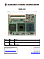
init CME-965 COM Express Computer-On-Module Based on Intel® Core 2 Duo LV CPU Revision Date Comment 1.0 03/30/10 Initial release 1.1 05/24/10 Update to block diagram 1.2 11/29/10 Minor updates FOR TECHNICAL SUPPORT PLEASE CONTACT: [email protected] Copyright 2010 Diamond Systems Corporation 1255 Terra Bella Ave. Mountain View, CA 94043 USA Tel 1-650-810-2500 Fax 1-650-810-2525 www.diamondsystems.com CONTENTS IMPORTANT SAFE-HANDLING INFORMATION ......................................................................................................3 1. INTRODUCTION .................................................................................................................................................4 1.1 Features .........................................................................................................................................................4 2. FUNCTIONAL OVERVIEW .................................................................................................................................6 2.1 Block Diagram ...............................................................................................................................................6 2.2 Board Dimensions, Mounting Holes, and Connectors...................................................................................7 2.3 Bus and Interface Connector Summary ........................................................................................................9 2.4 COM Express Bus Connectors ......................................................................................................................9 3. GETTING STARTED........................................................................................................................................ 10 3.1 COM Express Development Kits ................................................................................................................ 11 3.2 Preparing the Hardware ............................................................................................................................. 11 3.3 Booting the System .................................................................................................................................... 12 3.4 BIOS Setup Utility ....................................................................................................................................... 12 3.4.1 Main Setup Menu ............................................................................................................................... 12 3.4.2 Advanced Setup Menu ....................................................................................................................... 12 3.4.3 PCI/PnP Settings Menu ..................................................................................................................... 13 3.4.4 Boot Settings Menu ............................................................................................................................ 13 3.4.5 Security Settings Menu ...................................................................................................................... 13 3.4.6 Chipset Settings Menu ....................................................................................................................... 13 3.4.7 Exit ..................................................................................................................................................... 13 3.5 Operating System Drivers .......................................................................................................................... 14 3.6 BIOS Beep Sounds List .............................................................................................................................. 14 4. INTERFACE CONNECTOR DETAILS ............................................................................................................. 15 4.1 COM Express A-B Connector ..................................................................................................................... 16 4.1.1 USB signals ....................................................................................................................................... 18 4.1.2 Gigabit Ethernet (LAN) ....................................................................................................................... 18 4.1.3 AC‟97 Audio / High Definition Audio .................................................................................................. 18 4.1.4 PCI Express ....................................................................................................................................... 19 4.1.5 SATA .................................................................................................................................................. 19 4.1.6 General Purpose Inputs and Outputs (GPIO) .................................................................................... 20 4.1.7 Power and System Management ....................................................................................................... 20 4.1.8 LVDS Flat Panel ................................................................................................................................ 21 4.1.9 LPC Interface ..................................................................................................................................... 21 4.1.10 Analog VGA (CRT) ............................................................................................................................ 22 4.1.11 TV Out ................................................................................................................................................ 22 4.1.12 Miscellaneous Signals ....................................................................................................................... 23 4.2 COM Express C-D Connector .................................................................................................................... 24 4.2.1 IDE (PATA) Bus ................................................................................................................................. 26 4.2.2 PCI Bus Interface ............................................................................................................................... 27 4.2.3 PCI Express x16 Graphics (PEG) bus ............................................................................................... 28 5. APPENDIX: SYSTEM RESOURCES REFERENCE ....................................................................................... 28 5.1 BIOS Memory Mapping .............................................................................................................................. 28 5.2 I/O Port Address Map ................................................................................................................................. 29 5.3 Interrupt Request (IRQ) Lines .................................................................................................................... 30 5.4 BIOS Beep Codes ...................................................................................................................................... 31 5.4.1 Boot Block Beep Codes ..................................................................................................................... 31 5.4.2 Post BIOS Beep Codes ..................................................................................................................... 32 5.4.3 Troubleshooting Post BIOS Beep Codes .......................................................................................... 32 5.4.4 Boot Block Initialization Code Checkpoints ....................................................................................... 33 5.4.5 Boot Block Recovery Code Checkpoints ........................................................................................... 34 5.4.6 POST Code Checkpoints ................................................................................................................... 35 5.4.7 DIM Code Checkpoints ...................................................................................................................... 38 5.4.8 ACPI Runtime Checkpoints ............................................................................................................... 39 CME-965 User Manual 1.2 www.diamondsystems.com Page 2 IMPORTANT SAFE-HANDLING INFORMATION WARNING: ESD-Sensitive Electronic Equipment! Observe ESD-safe handling procedures when working with this product. Always use this product in a properly grounded work area and wear appropriate ESD-preventive clothing and/or accessories. Always store this product in ESD-protective packaging when not in use. Safe Handling Precautions The CME-965 contains numerous I/O connectors that connect to sensitive electronic components. This creates many opportunities for accidental damage during handling, installation and connection to other equipment. The list here describes common causes of failure found on boards returned to Diamond Systems for repair. This information is provided as a source of advice to help you prevent damaging your Diamond (or any vendor‟s) embedded computer boards. ESD damage – This type of damage is almost impossible to detect, because there is no visual sign of failure or damage. The symptom is that the board simply stops working, because some component becomes defective. Usually the failure can be identified and the chip can be replaced. To prevent ESD damage, always follow proper ESD-prevention practices when handling computer boards. Damage during handling or storage – On some boards we have noticed physical damage from mishandling. A common observation is that a screwdriver slipped while installing the board, causing a gouge in the PCB surface and cutting signal traces or damaging components. Another common observation is damaged board corners, indicating the board was dropped. This may or may not cause damage to the circuitry, depending on what is near the corner. Most of our boards are designed with at least 25 mils clearance between the board edge and any component pad, and ground / power planes are at least 20 mils from the edge to avoid possible shorting from this type of damage. However these design rules are not sufficient to prevent damage in all situations. A third cause of failure is when a metal screwdriver tip slips, or a screw drops onto the board while it is powered on, causing a short between a power pin and a signal pin on a component. This can cause overvoltage / power supply problems described below. To avoid this type of failure, only perform assembly operations when the system is powered off. Sometimes boards are stored in racks with slots that grip the edge of the board. This is a common practice for board manufacturers. However our boards are generally very dense, and if the board has components very close to the board edge, they can be damaged or even knocked off the board when the board tilts back in the rack. Diamond recommends that all our boards be stored only in individual ESD-safe packaging. If multiple boards are stored together, they should be contained in bins with dividers between boards. Do not pile boards on top of each other or cram too many boards into a small location. This can cause damage to connector pins or fragile components. Power supply wired backwards – Our power supplies and boards are not designed to withstand a reverse power supply connection. This will destroy each IC that is connected to the power supply. In this case the board will most likely will be unrepairable and must be replaced. A chip destroyed by reverse power or by excessive power will often have a visible hole on the top or show some deformation on the top surface due to vaporization inside the package. Check twice before applying power! CME-965 User Manual 1.2 www.diamondsystems.com Page 3 1. INTRODUCTION The CME-965 is a highly integrated computer-on-module (COM) based on the low power, high performance Intel® Core 2 Duo LV processor clocked at up to 1.6GHz. The module is equipped with up to 4GB of DDR2 SDRAM and provides interfaces for high-resolution CRTs and LVDS-interfaced LCDs, PCI Express x16 Graphics (PEG), gigabit Ethernet, SATA drives, IDE, USB peripherals, and audio. Additionally, the CME-965 offers a high degree of system expansion flexibility via the presence of both PCI Express and PCI buses on its COM Express Type 2 compliant baseboard interface connectors. 1.1 Features Processor: o 1.6GHz Intel Core 2 Duo LV o 800MHz front-side bus o 4MB L2 cache Chipset: Intel 965GME with Intel ICH8M 2 200-pin SO-DIMM sockets, for up to 4GB DDR2 SDRAM (533/667MHz) Graphics: o Chipset: Integrated Intel® Graphics Media Accelerator x3100 o Provides three display interfaces: Analog VGA RGB support up to 2048 x 1536 resolution TV-out support NTSC/PAL up to HDTV 1080P LCD: Dual Channel 24-bit LVDS Audio: o AC‟97 link o Mic in, line in/out signals USB interfaces: 8 USB 2.0 ports Networking: 10/100/1000Mbps Ethernet (Realtek RTL8111B PCIe Gigabit Ethernet controller) Mass storage interface: o 3 SATA ports with 150MB/s maximum data rate o 1 PATA port supports 2 IDE devices Keyboard/mouse: USB keyboard/mouse devices supported Other: o o o o PC speaker interface Watchdog timer with 1-255 levels, reset 8-bit programmable digital I/O port SMBus serial buses Three system expansion buses: o PCI Express: 1 x16 link and 4 x1 links o 4 32-bit PCI bus masters o LPC bus Power: o +12VDC main power; +5VDC standby power o Power requirement: 12W idle, 24W loaded Operating environment: o o o Operating temperature -40 C to +85 C o Operating humidity 0 to 90% (non-condensing) CME-965 User Manual 1.2 www.diamondsystems.com Page 4 Dimensions: o COM Express Basic form-factor with Type 2 bus o 4.9 x 3.7 inches (125 x 95 mm) Weight: 2.8 oz (79 g) Software: o BIOS: AMI PnP flash BIOS o Operating systems supported: Windows XP and Linux 2.6 (contact Diamond for others) Note: The COM Express specification is available from the PICMG organization (http://www.picmg.org). The COM Express Tutorial and COM Express Design Guide are available for download from the PICMG organization COM Express website located at: http://www.picmg.org/v2internal/COMExpress.htm CME-965 User Manual 1.2 www.diamondsystems.com Page 5 2. FUNCTIONAL OVERVIEW 2.1 Block Diagram Figure 1 shows the CME-965 functional blocks, bus, and peripheral interface signals. Figure 1: Functional Block Diagram CME-965 User Manual 1.2 www.diamondsystems.com Page 6 2.2 Board Dimensions, Mounting Holes, and Connectors The two diagrams below show the mechanical dimensions of the CME-965‟s board outline and five mounting holes, as well as the position of all connectors on both the top and bottom sides of the board. Unit: mm Figure 2: Board Layout – Top CME-965 User Manual 1.2 www.diamondsystems.com Page 7 Figure 3: Board Layout – Bottom CME-965 User Manual 1.2 www.diamondsystems.com Page 8 2.3 Bus and Interface Connector Summary The CME-965 has two 2x110-pin interface connectors, as listed in the tables below which are defined in accordance with the PICMG COM Express Specification. Signal functions relating to all of the module‟s interface connectors are discussed in greater detail in Section 4 of this document. 2.4 COM Express Bus Connectors Connector Location Pins Function COM Express Bottom A-B bus 2x110 USB, gigabit Ethernet, PCI Express, AC‟97 audio, SATA, LVDS, LPC, VGA (CRT), LAN, TV Out, power and ground interfaces, and system and power management. COM Express Bottom C-D bus 2x110 PCI bus, IDE (PATA) bus, PCI Express x16 Graphics (PEG), and power and ground signals. CME-965 User Manual 1.2 www.diamondsystems.com Page 9 3. GETTING STARTED This section of the CME-965 User Manual covers basic hardware setup, power connection, system boot-up, and initial software configuration. First-time CME-965 users normally receive the product in conjunction with one of Diamond‟s Development Kits, which provide everything needed to ensure rapid application development. Important Safe-Handling Information WARNING: ESD-Sensitive Electronic Equipment! Observe ESD-safe handling procedures when working with this product. Always use this product in a properly grounded work area and wear appropriate ESD-preventive clothing and/or accessories. Always store this product in ESD-protective packaging when not in use. Please refer to page 3 of this manual (“Important Safe-Handling Information”) for further details. CME-965 User Manual 1.2 www.diamondsystems.com Page 10 3.1 COM Express Development Kits To facilitate evaluation and development, Diamond‟s COM Express are normally supplied in conjunction with one of Diamond‟s COM Express development kits (pictured below). This approach increases project efficiency and reduces risks by providing a known good environment for rapid application development. CME-965 Development Kit with Magellan Baseboard The baseboards in Diamond‟s COM Express development kits provide standardized I/O connectors (either on-board or via an included transition cable kit), for quick and easy access to nearly all system interfaces. They also feature a variety of expansion slots and sockets, for flexible system expansion. The kits – which include both generic models and application-oriented baseboards in various form-factors – also generally extend the COM Express module‟s functionality by adding Ethernet and serial ports, solid-state media sockets, and more. Additionally, the kits include pre-installed system RAM, drivers for Linux and Windows operation, and full documentation. 3.2 Preparing the Hardware If it is not already installed on the baseboard, carefully plug the CME-965 into the baseboard‟s COM Express bus connectors. Place the heatsink or heat-spreader supplied with the CME-965 on top of the module, positioning it so that its mounting holes line up with those of the module. Then, affix the module and heatsink to the baseboard using the provided hardware. Connect a USB keyboard, USB mouse, monitor, and mass storage devices to the appropriate connectors on the baseboard. Refer to the baseboard‟s User Manual for peripheral compatibility and interface cabling considerations. CME-965 User Manual 1.2 www.diamondsystems.com Page 11 3.3 Booting the System Power-up the display, and then power-up the system power supply. The CME-965 module should begin its boot-up sequence immediately, as evidenced by BIOS messages on the connected display. You can use the BIOS Setup utility and install an operating system on the boot drive just as you would on a normal desktop PC. 3.4 BIOS Setup Utility The BIOS Setup utility program is used for specifying the system configurations and settings. The BIOS ROM of the system stores the Setup utility. When you turn on the computer, the BIOS is immediately activated. The following menus/options are available: Main Setup Menu Advanced Setup Menu PCI/PnP Setup Menu Boot Setup Menu Security Setup Menu Chipset Setup Menu Exit Use the left/right arrow keys to highlight a particular configuration screen from the top menu bar, or use the down arrow key to access and configure the information in the menus which are described below. 3.4.1 Main Setup Menu This menu allows you to select configuration options for the following: System Time System Date 3.4.2 Advanced Setup Menu This menu allows you to select configuration options for the following: CPU Configuration – Settings for Hardware Prefetcher, Adjacent Cache Line Prefetch, Cache L1 & L2, Max CPUID Value Limit, Vanderpool Technology, Core Multi-Processing, and Intel SpeedStep Technology. IDE Configuration – Settings for hard drives (Primary/Secondary/Third IDE, Master/Slave). Floppy Configuration – Settings for the type of floppy drive installed on the system. Super IO Configuration – Settings for Onboard Floppy Controller, Serial Port1 / Port2 Address, Serial Port2 Mode, Parallel Port Address, Parallel Port Mode, Parallel Port IRQ, Restore on AC Power Loss by IO. Hardware Health Configuration – Settings for System / CPU Temperature 1, CPU / System Fan Speed, Vcore (CPU voltage), +5.0V / +3.3V / +12.0V / 5Vsb / VBAT (standby and battery voltage). ACPI Configuration – Settings for Suspend mode. AHCI Configuration – Settings for AHCI Ports. APM Configuration – Settings for Power Management/APM, Video Power Down Mode, Hard Disks Power Down Mode, Suspend Time Out, Keyboard & PS/2 Mouse, Power Button Mode, Advanced Resume Event Controls, Resume on PME#, Resume on RTC Alarm. CME-965 User Manual 1.2 www.diamondsystems.com Page 12 MPS Configuration – Settings for MPS Revision (multi-processor version control). USB Configuration – Settings for Legacy USB Support, USB 2.0 Controller Mode, BIOS EHCI Hand-Off, USB Mass Storage Reset Delay, Emulation Type (floppy/hard drive). Remote Access Configuration – Settings for Remote Access, Serial port number, Base Address IRQ. 3.4.3 PCI/PnP Settings Menu This menu allows you to select configuration options for the following: Clear NVRAM Plug & Play O/S PCI Latency Timer Allocate IRQ to PCI VGA IRQ3 - IRQ15 DMA Channel 0 - DMA Channel 7 Reserved Memory Size 3.4.4 Boot Settings Menu This menu allows you to select configuration options for the following: Boot Device Priority Hard Disk Drives Removable Drives Quick Boot Bootup Num-Lock LAN Boot Function 3.4.5 Security Settings Menu This menu allows you to select configuration options for the following: Supervisor Password & User Password Boot Sector Virus Protection 3.4.6 Chipset Settings Menu This menu allows you to select configuration options for the following: North Bridge Chipset Configuration – Settings for Boots Graphic Adapter Priority, Internal Graphic Mode Select, Video Function Configuration, DVMT Mode and Memory, Boot Display (CRT, LVDS), Flat Panel Type, TV Standard, Spread Spectrum Clock. South Bridge Chipset Configuration – Settings for USB Function (active ports), USB 2.0 Controller, HDA Controller, SLP_S4# Min. Assertion Width, Onboard LAN1. 3.4.7 Exit This selection saves changes and exits the BIOS Setup Utility. CME-965 User Manual 1.2 www.diamondsystems.com Page 13 3.5 Operating System Drivers Drivers for Windows XP and Linux 2.6, if required, are included on the Software and Documentation CD that is provided along with the CME-965 or in its Development Kit. To locate the CME-965 module‟s software drivers on the CD, view the index.html file in the CD‟s root directory, locate “Computer-on-Modules,” and then click on “CME965.” This software is also available for download from Diamond‟s website. 3.6 BIOS Beep Sounds List Post BIOS Beep Codes Number of Beeps Description 1 Memory refresh timer error. 2 Parity error in base memory (first 64KB block) 3 Base memory read/write test error 4 Motherboard timer not operational 5 Processor error 6 8042 Gate A20 test error (cannot switch to protected mode) 7 General exception error (processor exception interrupt error) 8 Display memory error (system video adapter) 9 AMIBIOS ROM checksum error 10 CMOS shutdown register read/write error More BIOS information is included in the Appendix. CME-965 User Manual 1.2 www.diamondsystems.com Page 14 4. INTERFACE CONNECTOR DETAILS This section describes the functions available on the COM Express A-B and C-D interface connectors. Note: The COM Express specification is available from the PICMG organization (http://www.picmg.org). The COM Express Tutorial and COM Express Design Guide are available for download from the PICMG organization COM Express website located at: http://www.picmg.org/v2internal/COMExpress.htm. CME-965 User Manual 1.2 www.diamondsystems.com Page 15 4.1 COM Express A-B Connector The 2x110-pin, high-density COM Express A-B connector implements the board‟s USB, PCI Express, SATA, LVDS, LPC, AC‟97 (audio), VGA (CRT), LAN, power and ground interfaces, and system and power management, as indicated in the table below. Further information regarding each of these signal groups follows the table. (Note: Pins designated “NC” should be left unconnected.) GND B1 A1 GND USB7- B36 A36 USB6- GBE0_ACT# B2 A2 GBE0_MDI3- USB7+ B37 A37 USB6+ LPC_FRAME# B3 A3 GBE0_MDI3+ USB_4_5_OC# B38 A38 USB_6_7_OC# LPC_AD0 B4 A4 GBE0_LINK100# USB5- B39 A39 USB4- LPC_AD1 B5 A5 GBE0_LINK1000# USB5+ B40 A40 USB4+ LPC_AD2 B6 A6 GBE0_MDI2- GND B41 A41 GND LPC_AD3 B7 A7 GBE0_MDI2+ USB3- B42 A42 USB2- LPC_DRQ0# B8 A8 GBE0_LINK# USB3+ B43 A43 USB2+ LPC_DRQ1# B9 A9 GBE0_MDI1- USB_0_1_OC# B44 A44 USB_2_3_OC# LPC_CLK B10 A10 GBE0_MDI1+ USB1- B45 A45 USB0- GND B11 A11 GND USB1+ B46 A46 USB0+ PWRBTN# B12 A12 GBE0_MDI0- EXCD1_PERST# B47 A47 VCC_RTC SMB_CK B13 A13 GBE0_MDI0+ EXCD1_CPPE# B48 A48 EXCD0_PERST# SMB_DAT B14 A14 GBE0_CTREF SYS_RESET# B49 A49 EXCD0_CPPE# SMB_ALERT# B15 A15 SUS_S3# CB_RESET# B50 A50 LPC_SERIRQ SATA1_TX+ B16 A16 SATA0_TX+ GND B51 A51 GND SATA1_TX- B17 A17 SATA0_TX- PCIE_RX5+ B52 A52 PCIE_TX5+ SUS_STAT# B18 A18 SUS_S4# PCIE_RX5- B53 A53 PCIE_TX5- SATA1_RX+ B19 A19 SATA0_RX+ GPO1 B54 A54 GPI0 SATA1_RX- B20 A20 SATA0_RX- PCIE_RX4+ B55 A55 PCIE_TX4+ GND B21 A21 GND PCIE_RX4- B56 A56 PCIE_TX4- NC B22 A22 SATA2_TX+ GPO2 B57 A57 GND NC B23 A23 SATA2_TX- PCIE_RX3+ B58 A58 PCIE_TX3+ PWR_OK B24 A24 SUS_S5# PCIE_RX3- B59 A59 PCIE_TX3- NC B25 A25 SATA2_RX+ GND B60 A60 GND NC B26 A26 SATA2_RX- PCIE_RX2+ B61 A61 PCIE_TX2+ WDT B27 A27 BATLOW# PCIE_RX2- B62 A62 PCIE_TX2- AC_SDIN2 B28 A28 SATA_ACT# GPO3 B63 A63 GPI1 AC_SDIN1 B29 A29 AC_SYNC PCIE_RX1+ B64 A64 PCIE_TX1+ AC_SDIN0 B30 A30 AC_RST# PCIE_RX1- B65 A65 PCIE_TX1- GND B31 A31 GND WAKE0# B66 A66 GND SPKR B32 A32 AC_BITCLK WAKE1# B67 A67 GPI2 I2C_CK B33 A33 AC_SDOUT PCIE_RX0+ B68 A68 PCIE_TX0+ I2C_DAT B34 A34 BIOS_DISABLE# PCIE_RX0- B69 A69 PCIE_TX0- THRM# B35 A35 THRMTRIP# GND B70 A70 GND CME-965 User Manual 1.2 www.diamondsystems.com Page 16 LVDS_B0+ B71 A71 LVDS_A0+ VGA_GRN B91 A91 RESERVED LVDS_B0- B72 A72 LVDS_A0- VGA_BLU B92 A92 RESERVED LVDS_B1+ B73 A73 LVDS_A1+ VGA_HSYNC B93 A93 GPO0 LVDS_B1- B74 A74 LVDS_A1- VGA_VSYNC B94 A94 RESERVED LVDS_B2+ B75 A75 LVDS_A2+ VGA_I2C_CK B95 A95 RESERVED LVDS_B2- B76 A76 LVDS_A2- VGA_I2C_DAT B96 A96 GND LVDS_B3+ B77 A77 LVDS_VDD_EN TV_DAC_A B97 A97 VCC_12V LVDS-B3- B78 A78 LVDS_A3+ TV_DAC_B B98 A98 VCC_12V LVDS_BKLT_EN B79 A79 LVDS_A3- TV_DAC_C B99 A99 VCC_12V GND B80 A80 GND GND B100 A100 GND LVDS_B_CK+ B81 A81 LVDS_A_CK+ VCC_12V B101 A101 VCC_12V LVDS_B_CK- B82 A82 LVDS_A_CK- VCC_12V B102 A102 VCC_12V LVDS_BKLT_CTRL B83 A83 LVDS_I2C_CK VCC_12V B103 A103 VCC_12V VCC_5V_SBY B84 A84 LVDS_I2C_DAT VCC_12V B104 A104 VCC_12V VCC_5V_SBY B85 A85 GPI3 VCC_12V B105 A105 VCC_12V VCC_5V_SBY B86 A86 KBD_RST# VCC_12V B106 A106 VCC_12V VCC_5V_SBY B87 A87 KBD_A20GATE VCC_12V B107 A107 VCC_12V RESERVED B88 A88 PCIE_CLK_REF+ VCC_12V B108 A108 VCC_12V VGA_RED B89 A89 PCIE_CLK_REF- VCC_12V B109 A109 VCC_12V GND B90 A90 GND GND B110 A110 GND CME-965 User Manual 1.2 www.diamondsystems.com Page 17 4.1.1 USB signals These pins provide connections to the board‟s eight USB channels. For further information regarding the functions of the USB signals listed above, refer to the USB 2.0 Specification, available from the USB Implementers Forum (http://www.usb.org). 4.1.2 Signal Name Signal Function Direction USB[0:7]+ USB[0:7]- USB differential pairs, data channels 0 through 7. I/O USB_0_1_OC# USB over-current sense, USB channels 0 and 1. I USB_2_3_OC# USB over-current sense, USB channels 2 and 3. I USB_4_5_OC# USB over-current sense, USB channels 4 and 5. I USB_6_7_OC# USB over-current sense, USB channels 6 and 7. I Gigabit Ethernet (LAN) These pins provide connections to the GigE (LAN) interface. 4.1.3 Signal Name Signal Function Direction GBE0_MDI[0:3]+ GBE0_MDI[0:3]GBE0_ACT# Gigabit Ethernet Controller 0: Media Dependent Interface Differential Pairs 0,1,2,3. Gigabit Ethernet Controller 0 activity indicator. I/O GBE0_LINK# Gigabit Ethernet Controller 0 link indicator. O GBE0_LINK100# Gigabit Ethernet Controller 0 100Mbsp link indicator. O GBE0_LINK1000# Gigabit Ethernet Controller 0 1000Mbps link indicator. O GBE0_CTREF Reference voltage for carrier board Ethernet channel 0 magnetics center tap. REF O AC’97 Audio / High Definition Audio These pins provide connections to the high definition audio interface. Signal Name Signal Function Direction AC_RST# AC_SYNC Reset output to AC‟97 CODEC. 48KHz fixed-rate, sample-synchronization signal to the CODEC(s). 12.228MHz serial data clock generated by the external CODEC(s). Serial TDM data output to the CODEC. Serial TDM data inputs from up to 3 CODECs/ O O AC_BITCLK AC_SDOUT AC_SDIN[0:2] CME-965 User Manual 1.2 www.diamondsystems.com O O I Page 18 4.1.4 PCI Express These pins provide four PCI Express bus x1 links plus several other PCI Express-related signals. 4.1.5 Signal Name Signal Function Direction PCIE_TX[0:3]+ PCIE_TX[0:3]- PCI Express Differential Transmit Pairs 0 through 3. O PCIE_RX[0:3]+ PCIE_RX[0:3]- PCI Express Differential Receive Pairs 0 through 3. I PCIE_CLK_REF+/- Reference clock output for all PCI Express and PCI Express Graphics lanes. O EXCD[0:1]_CPPE# PCI Express Card capable card request, active low, one per card. I EXCD[0:1]_PERST# PCI Express Card reset, active low, one per card. O PCI_RESET# PCI Reset output, active low. O WAKE0# PCI Express wakeup signal. I SATA These pins carry signals for the three Serial ATA (SATA) ports. Signal Name Signal Function Direction SATA0_TX+ SATA0_TX SATA Channel 0 transmit differential pair. O SATA0_RX+ SATA0_RX SATA Channel 0 receive differential pair. I SATA1_TX+ SATA1_TX SATA Channel 1 transmit differential pair. O SATA1_RX+ SATA1_RX SATA Channel 1 receive differential pair. I SATA2_TX+ SATA2_TX SATA Channel 2 transmit differential pair. O SATA2_RX+ SATA2_RX SATA Channel 2 receive differential pair. I SATA_ACT# SATA activity indicator LED. O CME-965 User Manual 1.2 www.diamondsystems.com Page 19 4.1.6 General Purpose Inputs and Outputs (GPIO) These pins carry four general purpose input lines and four general purpose outputs. 4.1.7 Signal Name Signal Function Direction GPO[0:3] General purpose output pins. O GPI[0:3] General purpose input pins. I Power and System Management These pins support various power management and control functions. Signal Name Signal Function Direction PWRBTN# Power button to bring system out of S5 (soft off), active on rising edge. I SYS_RESET# Reset button input. I CB_RESET# Reset output from module to carrier board. O PWR_OK Power OK from main power supply. I SUS_STAT# Indicates imminent suspend operation; used to notify LPC devices. O SUS_S3# Indicates system is in Suspend to RAM state. O SUS_S4# Indicates system is in Suspend to Disk state. O SUS_S5# Indicates system is in Soft Off state. Also known as "PS_ON" and can be used to control an ATX power supply. O WAKE0# PCI Express wakeup signal. I WAKE1# General purpose wakeup signal. I BATLOW# Indicates that external battery is low. I THRM# Input from off-module temp sensor indicating an over-temp situation. I THERMTRIP# Active low output indicating that the CPU has entered thermal shutdown. O SMB_CK System Management Bus bidirectional clock line. I/O SMB_DAT System Management Bus bidirectional data line. I/O SMB_ALERT# System Management Bus Alert.. I CME-965 User Manual 1.2 www.diamondsystems.com Page 20 4.1.8 LVDS Flat Panel These pins carry data for graphical display on an LVDS panel, as indicated. 4.1.9 Signal Name Signal Function Direction LVDS_A[0:3]+ LVDS_A[0:3]- LVDS Channel A differential pairs. O LVDS_A_CK+ LVDS_A_CK LVDS Channel A differential clock. O LVDS_B[0:3]+ LVDS_B[0:3]- LVDS Channel B differential pairs. O LVDS_B_CK+ LVDS_B_CK LVDS Channel B differential clock. O LVDS_VDD_EN LVDS panel power enable. O LVDS_BKLT_EN LVDS panel backlight enable. O LVDS_BKLT_CTRL LVDS panel backlight brightness control. O LVDS_I2C_CK I2C clock output for LVDS display use. O LVDS_I2C_DAT I2C data line for LVDS display use. I/O LPC Interface These pins carry the Low Pin Count (LPC) interface signals, as indicated. Signal Name Signal Function Direction LPC_AD[0:3] LPC multiplexed address, command and data bus. I/O LPC_FRAME# LPC frame indicates the start of an LPC cycle. O LPC_DRQ[0:1]# LPC serial DMA request. I LPC_SERIRQ LPC serial interrupt. I/O LPC_CLK LPC clock output. O CME-965 User Manual 1.2 www.diamondsystems.com Page 21 4.1.10 Analog VGA (CRT) These pins carry video and timing data for graphical display on a TV device, as indicated. Signal Name Signal Function Direction VGA_RED Red for monitor. Analog DAC output, designed to drive a 37.5-Ohm equivalent load. O VGA_GRN Green for monitor. Analog DAC output, designed to drive a 37.5-Ohm equivalent load. O VGA_BLU Blue for monitor. Analog DAC output, designed to drive a 37.5-Ohm equivalent load. O VGA_HSYNC Horizontal sync output to VGA monitor O VGA_VSYNC Vertical sync output to VGA monitor O VGA_I2C_CK DDC clock line (I2C port dedicated to identify VGA monitor capabilities) O VGA_I2C_DAT DDC data line. I/O 4.1.11 TV Out These pins carry the composite video output signals. Signal Name Signal Function Direction TV_DAC_A TVDAC Channel A Output supports the following: Composite video: CVBS Component video: Chrominance (Pb) analog signal S-Video: not used O TV_DAC_B TVDAC Channel B Output supports the following: Composite video: not used Component video: Luminance (Y) analog signal. S-Video: Luminance analog signal. O TV_DAC_C TVDAC Channel C Output supports the following: Composite video: not used Component: Chrominance (Pr) analog signal. S-Video: Chrominance analog signal. O CME-965 User Manual 1.2 www.diamondsystems.com Page 22 4.1.12 Miscellaneous Signals These pins carry a number of utility signals. Signal Name Signal Function Direction SPKR Output for audio enunciator - the "speaker" in PC-AT systems O BIOS_DISABLE# Module BIOS disable input. I WDT Output indicating that a watchdog time-out event has occurred. O KBD_RST# Input to module from (optional) external keyboard controller that can force a reset. I KBD_A20GATE Input to module from (optional) external keyboard controller. I CME-965 User Manual 1.2 www.diamondsystems.com Page 23 4.2 COM Express C-D Connector The 210-pin, high-density COM Express C-D connector implements the IDE (PATA) bus, PCI bus, PCI Express x16 Graphics (PEG) bus, and power and ground signals as indicated in the table below. GND D1 C1 GND PCI_FRAME# D36 C36 PCI_DEVSEL# IDE_D5 D2 C2 IDE_D7 PCI_AD16 D37 C37 PCI_IRDY# IDE_D10 D3 C3 IDE_D6 PCI_AD18 D38 C38 PCI_C/BE2# IDE_D11 D4 C4 IDE_D3 PCI_AD20 D39 C39 PCI_AD17 IDE_D12 D5 C5 IDE_D15 PCI_AD22 D40 C40 PCI_AD19 IDE_D4 D6 C6 IDE_D8 GND D41 C41 GND IDE_D0 D7 C7 IDE_D9 PCI_AD24 D42 C42 PCI_AD21 IDE_REQ D8 C8 IDE_D2 PCI_AD26 D43 C43 PCI_AD23 IDE_IOW# D9 C9 IDE_D13 PCI_AD28 D44 C44 PCI_C/BE3# IDE_ACK# D10 C10 IDE_D1 PCI_AD30 D45 C45 PCI_AD25 GND D11 C11 GND PCI_IRQC# D46 C46 PCI_AD27 IDE_IRQ D12 C12 IDE_D14 IDE_A0 D13 C13 IDE_IORDY IDE_A1 D14 C14 IDE_IOR# IDE_A2 D15 C15 PCI_PME# IDE_CS1# D16 C16 PCI_IRQD# D47 C47 PCI_AD29 PCI_CLKRUN# D48 C48 PCI_AD31 PCI_M66EN D49 C49 PCI_IRQA# PCI_CLK D50 C50 PCI_IRQB# PCI_GNT2# GND D51 C51 GND (FIXED) IDE_CS3# D17 C17 PCI_REQ2# PEG_TX0+ D52 C52 PEG_RX0+ IDE_RESET# D18 C18 PCI_GNT1# PEG_TX0- D53 C53 PEG_RX0- PCI_GNT3# D19 C19 PCI_REQ1# PEG_LANE_RV# D54 C54 TYPE0# PCI_REQ3# D20 C20 PCI_GNT0# PEG_TX1+ D55 C55 PEG_RX1+ GND D21 C21 GND PEG_TX1- D56 C56 PEG_RX1- PCI_AD1 D22 C22 PCI_REQ0# TYPE2# D57 C57 TYPE1# PCI_AD3 D23 C23 PCI_RESET# PEG_TX2+ D58 C58 PEG_RX2+ PCI_AD5 D24 C24 PCI_AD0 PEG_TX2- D59 C59 PEG_RX2- PCI_AD7 D25 C25 PCI_AD2 GND D60 C60 GND PCI_C/BE0# D26 C26 PCI_AD4 PEG_TX3+ D61 C61 PEG_RX3+ PCI_AD9 D27 C27 PCI_AD6 PEG_TX3- D62 C62 PEG_RX3- PCI_AD11 D28 C28 PCI_AD8 RESERVED D63 C63 RESERVED PCI_AD13 D29 C29 PCI_AD10 RESERVED D64 C64 RESERVED PCI_AD15 D30 C30 PCI_AD12 PEG_TX4+ D65 C65 PEG_RX4+ GND D31 C31 GND PEG_TX4- D66 C66 PEG_RX4- PCI_PAR D32 C32 PCI_AD14 GND D67 C67 RESERVED PCI_SERR# D33 C33 PCI_C/BE1# PEG_TX5+ D68 C68 PEG_RX5+ PCI_STOP# D34 C34 PCI_PERR# PEG_TX5- D69 C69 PEG_RX5- PCI_TRDY# D35 C35 PCI_LOCK# GND D70 C70 GND CME-965 User Manual 1.2 www.diamondsystems.com Page 24 PEG_TX6+ D71 C71 PEG_RX6+ PEG_TX12+ D91 C91 PEG_RX12+ PEG_TX6- D72 C72 PEG_RX6- PEG_TX12- D92 C92 PEG_RX12- SDVO_I2C_CLK D73 C73 SDVO__I2C_DATA GND D93 C93 GND PEG_TX7+ D74 C74 PEG_RX7+ PEG_TX13+ D94 C94 PEG_RX13+ PEG_TX7- D75 C75 PEG_RX7- PEG_TX13- D95 C95 PEG_RX13- GND D76 C76 GND GND D96 C96 GND IDE_CBLID# D77 C77 RESERVED PEG_ENABLE# D97 C97 RESERVED PEG_TX8+ D78 C78 PEG_RX8+ PEG_TX14+ D98 C98 PEG_RX14+ PEG_TX8- D79 C79 PEG_RX8- PEG_TX14- D99 C99 PEG_RX14- GND D80 C80 GND GND D100 C100 GND PEG_TX9+ D81 C81 PEG_RX9+ PEG_TX15+ D101 C101 PEG_RX15+ PEG_TX9- D82 C82 PEG_RX9- PEG_TX15- D102 C102 PEG_RX15- RESERVED D83 C83 RESERVED GND D103 C103 GND GND D84 C84 GND VCC_12V D104 C104 VCC_12V PEG_TX10+ D85 C85 PEG_RX10+ VCC_12V D105 C105 VCC_12V PEG_TX10- D86 C86 PEG_RX10- VCC_12V D106 C106 VCC_12V GND D87 C87 GND VCC_12V D107 C107 VCC_12V PEG_TX11+ D88 C88 PEG_RX11+ VCC_12V D108 C108 VCC_12V PEG_TX11- D89 C89 PEG_RX11- VCC_12V D109 C109 VCC_12V GND D90 C90 GND GND D110 C110 GND CME-965 User Manual 1.2 www.diamondsystems.com Page 25 4.2.1 IDE (PATA) Bus This set of pins implements the module’s IDE bus which provide a single channel IDE interface supporting two standard IDE hard drives. Signal Name Signal Function Direction IDE_D[0:15] IDE_A[0:2] IDE_IOW# IDE_IOR# IDE_REQ Bidirectional data to/from IDE device. Address lines to IDE device. I/O write line to IDE device. Data latched on trailing (rising) edge. I/O read line to IDE device. IDE Device DMA Request. It is asserted by the IDE device to request a data transfer. IDE Device DMA Acknowledge. IDE Device Chip Select for 1F0h to 1FFh range. IDE Device Chip Select for 3F0h to 3FFh range. IDE device I/O ready input. Reset output to IDE device. Interrupt request from IDE device. Input from off-module hardware indicating the type of IDE cable being used. High indicates a 40-pin cable used for legacy IDE modes. Low indicates that an 80-pin cable with interleaved grounds is used. Such a cable is required for Ultra-DMA 66,100 and 133 modes. I/O O O O I IDE_ACK# IDE_CS1# IDE_CS3# IDE_IORDY IDE_RESET# IDE_IRQ IDE_CBLID# CME-965 User Manual 1.2 www.diamondsystems.com O O O I O I I Page 26 4.2.2 PCI Bus Interface This set of pins implements the module‟s PCI expansion bus. For further information regarding the functions of the PCI bus signals, refer to the PCI Bus Specification, available from the PCI Special Interest Group (http://www.pcisig.com/specifications). Signal Name Signal Function Direction PCI_AD[0:31] PCI_C/BE[0:3]# PCI_DEVSEL# PCI_FRAME# PCI_IRDY# PCI_TRDY# PCI_STOP# PCI_PAR PCI_PERR# PCI_REQ[0:3]# PCI_GNT[0:3]# PCI_RESET# PCI_LOCK# PCI_SERR# PCI bus multiplexed address and data lines PCI bus byte enable lines, active low PCI bus Device Select. PCI bus Frame control line. PCI bus Initiator Ready control line. PCI bus Target Ready control line. PCI bus STOP control line. PCI bus parity Parity Error. PCI bus master request input lines. PCI bus master grant output lines. PCI Reset output. PCI Lock control line. System Error: SERR# may be pulsed active by any PCI device that detects a system error condition. PCI Power Management Event: PCI peripherals drive PME# to wake system from low-power states S1–S5. Bidirectional pin used to support PCI clock run protocol for mobile systems. PCI interrupt request lines. PCI 33MHz clock output. Pull down strap. I/O I/O I/O I/O I/O I/O I/O I/O I/O I O O I/O I/O PCI_PME# PCI_CLKRUN# PCI_IRQ[A:D]# PCI_CLK PCI_M66EN CME-965 User Manual 1.2 www.diamondsystems.com I I/O I O I Page 27 4.2.3 PCI Express x16 Graphics (PEG) bus This set of pins drives a PCI Express x16 link, which may be used with an external high-performance PCI Express Graphics subsystem or other function that interfaces via a PCI Express x16 link. Signal Name Signal Function Direction PEG_RX[0:15]+ PEG_RX[0:15]- PCI Express Graphics receive differential pairs. I PEG_TX[0:15]+ PEG_TX[0:15]PCIE_CLK_REF+ PCIE_CLK_REFPEG_LANE_RV# PCI Express Graphics transmit differential pairs. O Reference clock output for all PCI Express and PCI Express Graphics lanes. PCI Express Graphics lane reversal input strap. Pull low on the carrier board to reverse lane order. PEG Enable function. Strap to enable PCI Express x16 external graphics interface. Pull low to disable internal graphics and enable the x16 interface. I2C based control signal (clock) for SDVO device. I2C based control signal (data) for SDVO device. O PEG_ENABLE# SDVO_I2C_CLK SDVO_I2C_DATA I I O I/O 5. APPENDIX: SYSTEM RESOURCES REFERENCE 5.1 BIOS Memory Mapping Address Device Description 00000h-9FFFFh DOS Kernel Area A0000h,BFFFFh EGA and VGA Video Buffer (128KB) C0000h-CFFFFh EGA/VGA ROM D0000h-DFFFFh Adaptor ROM E0000h-FFFFFh System BIOS CME-965 User Manual 1.2 www.diamondsystems.com Page 28 5.2 I/O Port Address Map Each peripheral device in the system is assigned a set of I/O port addresses which also becomes the identity of the device. The following table lists the I/O port addresses used. (Note: IDE currently is not supported on the CME-965.) Address Device Description 0000h - 0000Fh DMA Controller 0080h - 009Fh DMA Controller 00C0h - 00DFh DMA Controller 0020h, 0021h Programmable Interrupt Controller 00A0h, 00A1h Programmable Interrupt Controller 0040h - 0043h System Timer 0044h - 0047h System Timer 0060h - 0064h Keyboard Controller 0070h - 0073h System CMOS/Real Time Clock 00F0h - 00FFh Math Co-Processor 01F0h-01F7h Primary IDE 0274h-0277h ISAPNP Read Data Port 0279h , 0A79h ISAPnP Configuration 02F8h-02FFh COM_2 (If use) 0378h-037Ah Parallel Port (If use) 03B0h-03BFh MDA/MGA 03C0h-03CFh EGA/VGA 03D4h-03D9h CGA CRT register 03F0h-03F7h Floppy Diskette 03F6h-03F6h Primary IDE 03F8h-03FFh COM_1 (If use) 0400h-041F South Bridge SMB 04D0h-04D1h IRQ Edge/level control ports 0500h-053Fh South Bridge GPIO 0800h-087Fh ACPI 0A00h-0A07h PME CME-965 User Manual 1.2 www.diamondsystems.com Page 29 0A10h-0A17h Hardware Monitor 0CF8h PCI Configuration address 0CFCh PCI Configuration Data 5.3 Interrupt Request (IRQ) Lines Peripheral devices use interrupt request lines to notify CPU for the service required. The following table shows the IRQ used by the devices on board. IRQ Level Function IRQ 00 System Timer IRQ 01 Standard 101/102-Key or Microsoft Natural PS/2 Keyboard IRQ 02 VGA and Link to Secondary PIC IRQ 03 Communications Port (COM2) IRQ 04 Communications Port (COM1) IRQ 05 PCI Device IRQ 06 Standard floppy disk controller IRQ 07 Parallel Port IRQ 08 System CMOS/real time clock IRQ 09 Microsoft ACPI-Compliant System IRQ 10 PCI Device IRQ 11 PCI Device IRQ 12 PS/2 Compatible Mouse IRQ 13 PFY exception IRQ 14 Primary IDE Channel IRQ 15 PCI Device CME-965 User Manual 1.2 www.diamondsystems.com Page 30 5.4 BIOS Beep Codes This section contains BIOS codes and troubleshooting information. 5.4.1 Boot Block Beep Codes Number of Beeps Description 1 Insert diskette in floppy drive A: 2 „AMIBOOT.ROM‟ file not found in root directory of diskette in A: 3 Insert next diskette if multiple diskettes are used for recovery 4 Flash Programming successful 5 Floppy read error 6 Keyboard controller BAT command failed 7 No Flash EPROM detected 8 Floppy controller failure 9 Boot Block BIOS checksum error 10 Flash Erase error 11 Flash Program error 12 „AMIBOOT.ROM‟ file size error CME-965 User Manual 1.2 www.diamondsystems.com Page 31 5.4.2 5.4.3 Post BIOS Beep Codes Number of Beeps Description 1 Memory refresh timer error 2 Parity error in base memory (first 64KB block) 3 Base memory read/write test error 4 Motherboard timer not operational 5 Processor error 6 8042 Gate A20 test error (cannot switch to protected mode) 7 General exception error (processor exception interrupt error) 8 Display memory error (system video adapter) 9 AMIBIOS ROM checksum error 10 CMOS shutdown register read/write error Troubleshooting Post BIOS Beep Codes Number of Beeps Description 1, 2 or 3 4-7, 9-11 8 Reseat the memory, or replace with known good modules Fatal error indicating a serious problem with the system System video adapter failure CME-965 User Manual 1.2 www.diamondsystems.com Page 32 5.4.4 Boot Block Initialization Code Checkpoints Checkpoint Description Before D0 If boot block debugger is enabled, CPU cache-as-RAM functionality is enabled at this point. Stack will be enabled from this point. D0 Early Boot Strap Processor (BSP) initialization like microcode update, frequency and other CPU critical initialization. Early chipset initialization is done. D1 Early super I/O initialization is done including RTC and keyboard controller. Serial port is enabled at this point if needed for debugging. NMI is disabled. Perform keyboard controller BAT test. Save power-on CPUID value in scratch CMOS. Go to flat mode with 4GB limit and GA20 enabled. D2 Verify the boot block checksum. System will hang here if checksum is bad. D3 Disable cache before memory detection. Execute full memory sizing module. If memory sizing module not executed, start memory refresh and do memory sizing in boot block code. Do additional chipset initialization. Re-enable cache. Verify that flat mode is enabled. D4 Test base 512KB memory. Adjust policies and cache first 8MB. Set stack. D5 Boot block code is copied from ROM to lower system memory and control is given to it. BIOS now executes out of RAM. Copies compressed boot block code to memory in right segments. Copies BIOS from ROM to RAM for faster access. Performs main BIOS checksum and updates recovery status accordingly. D6 Both key sequence and OEM specific method is checked to determine if BIOS recovery is forced. If BIOS recovery is necessary, control flows to checkpoint E0. See Boot Block Recovery Code Checkpoints section of document for more information. D7 Restore CPUID value back into register. The Boot Block Runtime interface module is moved to system memory and control is given to it. Determine whether in memory. D8 The Runtime module is uncompressed into memory. CPUID information is stored in memory. D9 Store the Uncompressed pointer for future use in PMM. Copying Main BIOS into memory. Leaves all RAM below 1MB Read-Write including E000 and F000 shadow areas but closing SMRAM. DA Restore CPUID value back into register. Give control to BIOS POS (ExecutePOSTKernel). See POST Code Checkpoints section of document for more information. DC System is waking from ACPI S3 state. E1 - E8 EC - EE OEM memory detection/configuration error. This range is reserved for chipset vendors and system manufacturers. The error associated with this value may be different from one platform to be next. CME-965 User Manual 1.2 www.diamondsystems.com Page 33 5.4.5 Boot Block Recovery Code Checkpoints The boot block recovery code gets control when the BIOS determines that a BIOS recovery needs to occur because the user has forced the update or the BIOS checksum is corrupt. The following table describes the type of checkpoints that may occur during the boot block recovery portion of the BIOS. Checkpoint Description E0 Initialize the floppy controller in the super I/O. Some interrupt vectors are initialized. DMA controller is initialized. 8259 interrupt controller is initialized. L2 cache is enabled. E9 Set up floppy controller and data. Attempt to read from floppy. EA Enable ATAPI hardware. Attempt to read from ARMD and ATAPI CDROM. EB Disable ATAPI hardware. Jump back to checkpoint E9. EF Read error occurred on media. Jump back to checkpoint EB. F0 Search for pre-defined recovery file name in root directory. F1 Recovery file not found. F2 Start reading FAT table and analyze FAT to find the clusters occupied by the recovery file. F3 Start reading the recovery file cluster by cluster. F5 Disable L1 cache. FA Check the validity of the recovery file configuration to the current configuration of the flash part. FB Make flash write enabled through chipset and OEM specific method. Detect proper flash part. Verify that the found flash part size equals the recovery file size. F4 The recovery file size does not equal the found flash part size. FC Erase the flash part. FD Program the flash part. FF The flash has been updated successfully. Make flash write disabled. Disable ATAPI hardware. Restore CPUID value back into register. Give control to F000 ROM at F000:FFF0h. CME-965 User Manual 1.2 www.diamondsystems.com Page 34 5.4.6 POST Code Checkpoints The POST code checkpoints are the largest set of checkpoints during the BIOS pre-boot process. The following table describes the type of checkpoints that may occur during the POST portion of the BIOS. Checkpoint Description 03 Disable NMI, Parity, video for EGA, and DMA controllers. Initialize BIOS, POST, Runtime data area. Also initialize BIOS modules on POST entry and GPNV area. Initialized CMOS as mentioned in the Kernel Variable "wCMOSFlags." 04 Check CMOS diagnostic byte to determine if battery power is OK and CMOS checksum is OK. Verify CMOS checksum manually by reading storage area. If the CMOS checksum is bad, update CMOS with power-on default values and clear passwords. Initialize status register A. Initializes data variables that are based on CMOS setup questions. Initializes both the 8259 compatible PICs in the system. 05 Initializes the interrupt controlling hardware (generally PIC) and interrupt vector table. 06 Do R/W test to CH-2 count reg. Initialize CH-0 as system timer. Install the POSTINT1Ch handler. Enable IRQ-0 in PIC for system timer interrupt. Traps INT1Ch vector to "POSTINT1ChHandlerBlock." 07 Fixes CPU POST interface calling pointer. 07 Fixes CPU POST interface calling pointer. 08 Initializes the CPU. The BAT test is being done on KBC. Program the keyboard controller command byte is being done after Auto detection of KB/MS using AMI KB-5. C0 Early CPU Init Start -- Disable Cache - Init Local APIC C1 Set up boot strap processor Information C2 Set up boot strap processor for POST C5 Enumerate and set up application processors C6 Re-enable cache for boot strap processor C7 Early CPU Init Exit 0A Initializes the 8042 compatible Key Board Controller. 0B Detects the presence of PS/2 mouse. 0C Detects the presence of Keyboard in KBC port. 0E Testing and initialization of different Input Devices. Also, update the Kernel Variables. Traps the INT09h vector, so that the POST INT09h handler gets control for IRQ1. Uncompress all available language, BIOS logo, and Silent logo modules. 13 Early POST initialization of chipset registers. 20 Relocate System Management Interrupt vector for all CPU in the system. 24 Uncompress and initialize any platform specific BIOS modules. GPNV is initialized at this checkpoint. CME-965 User Manual 1.2 www.diamondsystems.com Page 35 2A Initializes different devices through DIM. See DIM Code Checkpoints section of document for more information. 2C Initializes different devices. Detects and initializes the video adapter installed in the system that have optional ROMs. 2E Initializes all the output devices. 31 Allocate memory for ADM module and uncompress it. Give control to ADM module for initialization. Initialize language and font modules for ADM. Activate ADM module. 33 Initializes the silent boot module. Set the window for displaying text information. 37 Displaying sign-on message, CPU information, setup key message, and any OEM specific information. 38 Initializes different devices through DIM. See DIM Code Checkpoints section of document for more information. USB controllers are initialized at this point. 39 Initializes DMAC-1 & DMAC-2. 3A Initialize RTC date/time. 3B Test for total memory installed in the system. Also, Check for DEL keys to limit memory test. Display total memory in the system. 3C Mid POST initialization of chipset registers. 40 Detect different devices (Parallel ports, serial ports, and Coprocessor in CPU, etc.) successfully installed in the system and update the BDA, EBDA, etc. 52 Updates CMOS memory size from memory found in memory test. Allocates memory for Extended BIOS Data Area from base memory. Programming the memory hole or any kind of implementation that needs an adjustment in system RAM size if needed. 60 Initializes NUM-LOCK status and programs the KBD typematic rate. 75 Initialize Int-13 and prepare for IPL detection. 78 Initializes IPL devices controlled by BIOS and option ROMs. 7C Generate and write contents of ESCD in NVRAM. 84 Log errors encountered during POST. 85 Display errors to the user and gets the user response for error. 87 Execute BIOS setup if needed/requested. Check boot password if installed. 8C Late POST initialization of chipset registers. 8D Build ACPI tables (if ACPI is supported). 8E Program the peripheral parameters. Enable/Disable NMI as selected. 90 Initialization of system management interrupt by invoking all handlers. A1 Line-up work needed before booting to OS. CME-965 User Manual 1.2 www.diamondsystems.com Page 36 A2 Takes care of runtime image preparation for different BIOS modules. Fill the free area in F000h segment with 0FFh. Initializes the Microsoft IRQ Routing Table. Prepares the runtime language module. Disables the system configuration display if needed. A4 Initialize runtime language module. Display boot option popup menu. A7 Displays the system configuration screen if enabled. Initialize the CPU‟s before boot, which includes the programming of the MTRR‟s. A9 Wait for user input at config display if needed. AA Uninstall POST INT1Ch vector and INT09h vector. AB Prepare BBS for Int 19 boot. Init MP tables. AC End of POST initialization of chipset registers. De-initializes the ADM module. B1 Save system context for ACPI. Prepare CPU for OS boot including final MTRR values. 00 Passes control to OS Loader (typically INT19h). CME-965 User Manual 1.2 www.diamondsystems.com Page 37 5.4.7 DIM Code Checkpoints The Device Initialization Manager (DIM) gets control at various times during BIOS POST to initialize different system buses. The following table describes the main checkpoints where the DIM module is accessed. Checkpoint Description 2A Initialize different buses and perform the following functions: Reset, Detect, and Disable (function 0); Static Device Initialization (function); Boot Output Device Initialization (function 2). Function 0 disables all device nodes, PCI devices, and PnP ISA cards. It also assigns PCI bus numbers. Function 1 initializes all static devices that include manual configured onboard peripherals, memory, and I/O decode windows in PCI-PCI bridges, and noncompliant PCI devices. Static resources are also reserved. Function 2 searches for and initializes any PnP, PCI, or AGP video devices. 38 Initialize different buses and perform the following functions: Boot Input Device Initialization (function 3); IPL Device Initialization (function 4); General Device Initialization (function 5). Function 3 searches for and configures PCI input devices and detects if system has standard keyboard controller. Function 4 searches for and configures all PnP and PCI boot devices. Function 5 configures all onboard peripherals that are set to an automatic configuration and configures all remaining PnP and PCI devices. While control is in the different functions, additional checkpoints are output to port 80h as a word value to identify the routines under execution. The low byte value indicates the main POST Code Checkpoint. The high byte is divided into two nibbles and contains two fields. The details of the high byte of these checkpoints are as follows: HIGH BYTE XY The upper nibble “X” indicates the function number that is being executed. “X” can be from 0 to 7. 0 = func#0, disable all devices on the BUS concerned. 2 = func#2, output device initialization on the BUS concerned. 3 = func#3, input device initialization on the BUS concerned. 4 = func#4, IPL device initialization on the BUS concerned. 5 = func#5, general device initialization on the BUS concerned. 6 = func#6, error reporting for the BUS concerned. 7 = func#7, add-on ROM initialization for all buses. CME-965 User Manual 1.2 www.diamondsystems.com Page 38 8 = func#8, BBS ROM initialization for all BUSes. The lower nibble 'Y' indicates the BUS on which the different routines are being executed. 'Y' can be from 0 to 5. 0 = Generic DIM (Device Initialization Manager). 1 = On-board System devices. 2 = ISA devices. 3 = EISA devices. 4 = ISA PnP devices. 5 = PCI devices. 5.4.8 ACPI Runtime Checkpoints ACPI checkpoints are displayed when an ACPI capable operating system either enters or leaves a sleep state. The following table describes the type of checkpoints that may occur during ACPI sleep or wake events. Checkpoint Description AC First ASL check point. Indicates the system is running in ACPI mode. AA System is running in APIC mode. 01, 02, 03, 04, 05 Entering sleep state S1, S2, S3, S4, or S5. 10, 20, 30, 40, 50 Waking from sleep state S1, S2, S3, S4, or S5. Note: Checkpoints may differ between different platforms based on system configuration. Checkpoints may change due to vendor requirements, system chipset or option ROMs from add-in PCI devices. CME-965 User Manual 1.2 www.diamondsystems.com Page 39