1
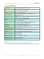
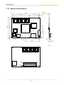
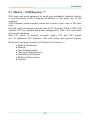
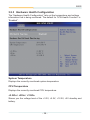
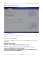
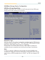
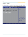
EmETXe-i0156
COM Express CPU Module
User’s Manual
Version 1.1
2011.06
This page is intentionally left blank.
Index
Table of Contents
Chapter 1 - Introduction............................................. 1
1.1 Copyright Notice........................................................2
1.2 Declaration of Conformity.........................................2
1.3 About This User’s Manual.........................................3
1.4 Warning.......................................................................3
1.5 Replacing the Lithium Battery..................................3
1.6 Technical Support......................................................4
1.7 Warranty......................................................................4
1.8 Packing List................................................................5
1.9 Ordering Information.................................................5
1.10 Specifications...........................................................6
1.11 Board Dimensions...................................................7
Chapter 2 - Installation............................................... 9
2.1
2.2
2.3
2.4
2.5
2.6
2.7
What is “ COM Express ”?......................................10
Block Diagram .........................................................11
Jumpers and Connectors........................................12
COM Express AB Connector...................................13
COM Express CD Connector..................................15
The Installation Paths of CD Driver........................17
How to Install Heatsink/Heat Spreader..................17
Chapter 3 - BIOS....................................................... 19
3.1 BIOS Main Setup......................................................20
3.2 Advanced Settings...................................................22
3.2.1 IDE Configuration..............................................23
3.2.2 Super IO Configuration.....................................26
3.2.3 Hardware Health Configuration........................28
3.2.4 USB Configuration.............................................29
3.3 Chipset Setting.........................................................31
3.3.1 North Bridge Chipset Configuration................32
3.3.2 South Bridge Chipset Configuration................34
3.4 Boot Setting..............................................................35
3.4.1 Boot Setting Configuration...............................36
-i-
Index
3.4.2 Boot Device Priority...........................................37
3.5 Security Setting.......................................................38
3.6 Exit Setting..............................................................39
3.7 Beep Sound codes list............................................41
3.7.1 Boot Block Beep Codes....................................41
3.7.2 POST BIOS Beep Codes....................................41
3.7.3 Troubleshooting POST BIOS Beep Codes......42
Appendix................................................................... 55
Appendix A:
Appendix B:
Appendix C:
Appendix D:
I/O Port Address Map...............................56
BIOS Memory Map...................................57
Interrupt Request Lines (IRQ).................58
Digital I/O Setting.....................................59
- ii -
Introduction
1
Chapter 1
Introduction
Chapter 1 - Introduction
-1-
Introduction
1.1 Copyright Notice
All Rights Reserved.
The information in this document is subject to change without prior notice in
order to improve the reliability, design and function. It does not represent a
commitment on the part of the manufacturer.
Under no circumstances will the manufacturer be liable for any direct, indirect,
special, incidental, or consequential damages arising from the use or inability
to use the product or documentation, even if advised of the possibility of such
damages.
This document contains proprietary information protected by copyright.
All rights are reserved. No part of this manual may be reproduced by any
mechanical, electronic, or other means in any form without prior written
permission of the manufacturer.
1.2 Declaration of Conformity
CE
This product has passed the CE test for environmental specifications when
shielded cables are used for external wiring. This kind of cable is available
from ARBOR. Please contact your local supplier for ordering information.
Test conditions for passing included the equipment being operated within an
industrial enclosure. In order to protect the product from being damaged by
ESD (Electrostatic Discharge) and EMI leakage, we strongly recommend the
use of CE-compliant industrial enclosure products.
FCC Class A
This device complies with Part 15 of the FCC Rules. Operation is subject
to the following two conditions : (1) this device may not cause harmful
interference, and (2) this device must accept any interference received,
including interference that may cause undesired operation.
RoHS
ARBOR Technology Corp. certifies that all components in its products are in
compliance and conform to the European Union’s Restriction of Use of Hazardous Substances in Electrical and Electronic Equipment (RoHS) Directive
2002/95/EC.
The above mentioned directive was published on 2/13/2003. The main purpose of the directive is to prohibit the use of lead, mercury, cadmium, hexavalent chromium, polybrominated biphenyls (PBB), and polybrominated diphenyl
ethers (PBDE) in electrical and electronic products. Member states of the EU
-2-
Introduction
are to enforce by 7/1/2006.
ARBOR Technology Corp. hereby states that the listed products do not contain unintentional additions of lead, mercury, hex chrome, PBB or PBDB that
exceed a maximum concentration value of 0.1% by weight or for cadmium
exceed 0.01% by weight, per homogenous material. Homogenous material
is defined as a substance or mixture of substances with uniform composition
(such as solders, resins, plating, etc.). Lead-free solder is used for all terminations (Sn(96-96.5%), Ag(3.0-3.5%) and Cu(0.5%)).
1.3 About This User’s Manual
This user’s manual provides general information and installation instructions
about the product. This User’s Manual is intended for experienced users and
integrators with hardware knowledge of personal computers. If you are not
sure about any description in this booklet. please consult your vendor before
further handling.
1.4 Warning
Single Board Computers and their components contain very delicate
Integrated Circuits (IC). To protect the Single Board Computer and its
components against damage from static electricity, you should always follow
the following precautions when handling it :
1. Disconnect your Single Board Computer from the power source when you
want to work on the inside.
2. Hold the board by the edges and try not to touch the IC chips, leads or circuitry.
3. Use a grounded wrist strap when handling computer components.
4. Place components on a grounded antistatic pad or on the bag that comes
with the Single Board Computer, whenever components are separated from
the system.
1.5 Replacing the Lithium Battery
Incorrect replacement of the lithium battery may lead to a risk of explosion.
The lithium battery must be replaced with an identical battery or a battery type
recommended by the manufacturer.
Do not throw lithium batteries into the trash-can. It must be disposed of in
accordance with local regulations concerning special waste.
-3-
Introduction
1.6 Technical Support
If you have any technical difficulties, please do not hesitate to call or e-mail our
customer service.
http://www.arbor.com.tw
E-mail:[email protected]
1.7 Warranty
This product is warranted to be in good working order for a period of two years
from the date of purchase. Should this product fail to be in good working order
at any time during this period, we will, at our option, replace or repair it at no
additional charge except as set forth in the following terms. This warranty does
not apply to products damaged by misuse, modifications, accident or disaster.
Vendor assumes no liability for any damages, lost profits, lost savings or any
other incidental or consequential damage resulting from the use, misuse of,
or inability to use this product. Vendor will not be liable for any claim made by
any other related party.
Vendors disclaim all other warranties, either expressed or implied, including
but not limited to implied warranties of merchantability and fitness for a
particular purpose, with respect to the hardware, the accompanying product’s
manual(s) and written materials, and any accompanying hardware. This limited
warranty gives you specific legal rights.
Return authorization must be obtained from the vendor before returned
merchandise will be accepted. Authorization can be obtained by calling or
faxing the vendor and requesting a Return Merchandise Authorization (RMA)
number. Returned goods should always be accompanied by a clear problem
description.
-4-
Introduction
1.8 Packing List
1 x EmETXe-i0156 COM Express CPU Module
1 x Driver CD
1 x Quick Installation Guide
If any of the above items is damaged or missing, contact your vendor
immediately.
1.9 Ordering Information
EmETXe-i0156/Z510PT
Intel® Menlow-XL Z510PT COM Express CPU Module,
soldered onboard 1GB SDRAM
EmETXe-i0156/Z530P
Intel® Menlow-XL Z530P COM Express CPU Module,
soldered onboard 1GB SDRAM
HS-0630-W2
Heatsink wave type (95 x 125 x18 mm)
HS-0630-F2
Heat spreader (95 x 125 x18 mm)
PBE-1700 R1.1
COM Express evaluation board in ATX form factor
CBK-04-1700-00
Cable kit for PBE-1700
1 x SATA cable
1 x COM port cable
1 x FDD cable
1 x IDE cable
-5-
Introduction
1.10 Specifications
Form Factor
COM Express Type 2 CPU Module
CPU
Intel® Atom™ Z510PT processor with 400MHz FSB or
Z530P processor with 533MHz
Chipset
Intel® Poulsbo US15WPT
System Memory
Soldered onboard DDR2 533MHz SDRAM 1GB,
upgradable to 2GB
VGA/LCD Controller
Integrated Intel® Graphics Media Accelerator 500, Analog
RGB/24-bit Single Channel LVDS
Ethernet
1 x Intel® 82574IT Gigabit Ethernet
BIOS
AMI PnP Flash BIOS
Storage
2 x Serial ATA with 300MB/s HDD transfer rate
1 x Ultra ATA, support 2 IDE devices
Serial Port
2 x COM ports (via PBE-1700)
Parallel Port
SPP/EPP/ECP mode (via PBE-1700)
Universal Serial Bus
8 x USB 2.0 ports
Keyboard/ Mouse
USB interfaced Keyboard and Mouse (via PBE-1700)
Digital I/O
8-bit Programmable Digital Input/ Output
Expansion Interface
5 x PCIex1 lane
4 x PCI masters
Operation Temp.
-20ºC ~ 70ºC (-4ºF ~ 158ºF)
Watchdog Timer
1~255 levels reset
Dimension (L x W)
125 x 95 mm (4.9" x 3.7")
Note:
1. The SATA (Serial ATA) is only supported in Windows XP SP3.
2. To connect an IDE HDD device, please use a flat cable that supports ATA 66/100.
-6-
Introduction
1.11 Board Dimensions
2.26 (NB)
125.00
76.00
41.00
4.00
26.83
57.53
44.45
1
4.00
95.00
87.00
AT
1.60
64.04
3.25
Unit: mm
D1
C1
D110
C110
B1
A1
B110
A110
-7-
Introduction
This page is intentionally left blank.
-8-
Installation
2
Chapter 2
Installation
Chapter 2 - Installation
-9-
Installation
2.1 What is “ COM Express ”?
With more and more demands on small and embedded industrial boards,
a multi-functioned COM (Computer-on-Module) is the great one of the
solutions.
COM Express, board-to-board connectors consist of two rows of 220 pins
each.
Row AB, which is required, provides pins for PCI Express, SATA, LVDS, LCD
channel, LPC bus, system and power management, VGA, LAN, and power
and ground interfaces.
Row CD, which is optional, provides legacy PCI and IDE signals
next to additional PCI Express, LAN and power and ground signals.
By the way, the target markets of COM will be focused on --
● Retail & Advertising
● Medical
● Test & Measurement
● Gaming & Entertainment
● Industrial & Automation
● Military & Government
● Security
- 10 -
Installation
2.2 Block Diagram
COM Express Type 2
System Block Diagram
Intel®
Z510PT/Z530P
Menlow-XL
Processor
FSB
400/533MHz
Onboard DDR2
up to 2GB SDRAM
SDVO
DDR2-533MHz
CH7317A
Analog RGB
LVDS 24-bit
HD Audio
PCI0
PCI2
PCI3
Connector CD
IDE ATA I/F
PCIe to PCI
PEX8112
PCIe x 1
USB Port 0 ~7
Intel®
Poulsbo
US15WPT
SCH
SMBus
SMBus
F75111RG
8 GPIO
LPC I/F
PCIe x 1
LPC I/F
EC ITE8512
BIOS ROM
SPI 8MB
I2C
PCIe switch
PEX8509
PCIe x 1
PCIe x 1
Giga LAN
Intel 82574IT
PCIe to SATA
JMB362 Controller
5 x PCIex1
- 11 -
GbE LAN
2 x SATA ports
Connector AB
PCI1
Installation
2.3 Jumpers and Connectors
1
D110
D1
C110
B110
C1
B1
A110
A1
- 12 -
Installation
2.4 COM Express AB Connector
B1
B2
B3
B4
B5
B6
B7
B8
B9
B10
B11
B12
B13
B14
B15
B16
B17
B18
B19
B20
B21
B22
B23
B24
B25
B26
B27
B28
B29
B30
B31
B32
B33
B34
B35
B36
B37
B38
B39
B40
B41
B42
B43
B44
B45
B46
B47
B48
B49
B50
B51
B52
B53
B54
B55
GND
GBE0_ACT#
LPC_FRAME#
LPC_AD0
LPC_AD1
LPC_AD2
LPC_AD3
N/C
N/C
LPC_CLK
GND
PWRBTN#
SMB_CK
SMB_DAT
SMB_ALERT#
SATA1_TX+
SATA1_TXN/C
SATA1_RX+
SATA1_RXGND
N/C
N/C
PWR_OK
N/C
N/C
WDT
N/C
N/C
AC_SDIN0
GND
SPKR
I2C_CK
I2C_DAT
THRM#
USB7USB7+
USB_4_5_OC#
USB5USB5+
GND
USB3USB3+
USB_0_1_OC#
USB1USB1+
EXCD1_PERST#
EXCD1_CPPE#
SYS_RESET#
CB_RESET#
GND
N/C
N/C
GPIO5
PCIE_RX4+
GND
GBE0_MDI3GBE0_MDI3+
GBE0_LINK100#
GBE0_LINK1000#
GBE0_MDI2GBE0_MDI2+
GBE0_LINK#
GBE0_MDI1GBE0_MDI1+
GND
GBE0_MDI0GBE0_MDI0+
GBE0_CTREF
SUS_S3#
SATA0_TX+
SATA0_TXN/C
SATA0_RX+
SATA0_RXGND
N/C
N/C
N/C
N/C
N/C
N/C
ATA_ACT#
AC_SYNC
AC_RST#
GND
AC_BITCLK
AC_SDOUT
N/C
THRMTRIP#
USB6USB6+
USB_6_7_OC#
USB4USB4+
GND
USB2USB2+
USB_2_3_OC#
USB0USB0+
VCC_RTC
EXCD0_PERST#
EXCD0_CPPE#
LPC_SERIRQ
GND
N/C
N/C
GPI0
PCIE_TX4+
- 13 -
A1
A2
A3
A4
A5
A6
A7
A8
A9
A10
A11
A12
A13
A14
A15
A16
A17
A18
A19
A20
A21
A22
A23
A24
A25
A26
A27
A28
A29
A30
A31
A32
A33
A34
A35
A36
A37
A38
A39
A40
A41
A42
A43
A44
A45
A46
A47
A48
A49
A50
A51
A52
A53
A54
A55
Installation
B56
B57
B58
B59
B60
B61
B62
B63
B64
B65
B66
B67
B68
B69
B70
B71
B72
B73
B74
B75
B76
B77
B78
B79
B80
B81
B82
B83
B84
B85
B86
B87
B88
B89
B90
B91
B92
B93
B94
B95
B96
B97
B98
B99
B100
B101
B102
B103
B104
B105
B106
B107
B108
B109
B110
PCIE_RX4GPIO6
PCIE_RX3+
PCIE_RX3GND
PCIE_RX2+
PCIE_RX2GPIO7
PCIE_RX1+
PCIE_RX1WAKE0#
N/C
PCIE_RX0+
PCIE_RX0GND
N/C
N/C
N/C
N/C
N/C
N/C
N/C
N/C
LVDS_BKLT_EN
GND
N/C
N/C
CKLVDS_BKLT_CTRL
VCC_5V_SBY
VCC_5V_SBY
VCC_5V_SBY
VCC_5V_SBY
RSVD
VGA_RED
GND
VGA_GRN
VGA_BLU
VGA_HSYNC
VGA_VSYNC
VGA_I2C_CK
VGA_I2C_DAT
N/C
N/C
N/C
GND
VCC_12V
VCC_12V
VCC_12V
VCC_12V
VCC_12V
VCC_12V
VCC_12V
VCC_12V
VCC_12V
GND
PCIE_TX4GND
PCIE_TX3+
PCIE_TX3GND
PCIE_TX2+
PCIE_TX2GPIO1
PCIE_TX1+
PCIE_TX1GND
GPIO2
PCIE_TX0+
PCIE_TX0GND
LVDS_A0+
LVDS_A0LVDS_A1+
LVDS_A1LVDS_A2+
LVDS_A2LVDS_VDD_EN
LVDS_A3+
LVDS_A3GND
LVDS_A_CK+
LVDS_A_CKLVDS_DDC_CLK
LVDS_DDC_DATA
GPIO3
KBD_RST#
KBD_A20GATE
PCIE0_CK_REF+
PCIE0_CK_REFGND
RSVD
RSVD
GPIO4
RSVD
RSVD
GND
VCC_12V
VCC_12V
VCC_12V
GND
VCC_12V
VCC_12V
VCC_12V
VCC_12V
VCC_12V
VCC_12V
VCC_12V
VCC_12V
VCC_12V
GND
- 14 -
A56
A57
A58
A59
A60
A61
A62
A63
A64
A65
A66
A67
A68
A69
A70
A71
A72
A73
A74
A75
A76
A77
A78
A79
A80
A81
A82
A83
A84
A85
A86
A87
A88
A89
A90
A91
A92
A93
A94
A95
A96
A97
A98
A99
A100
A101
A102
A103
A104
A105
A106
A107
A108
A109
A110
Installation
2.5 COM Express CD Connector
D1
D2
D3
D4
D5
D6
D7
D8
D9
D10
D11
D12
D13
D14
D15
D16
D17
D18
D19
D20
D21
D22
D23
D24
D25
D26
D27
D28
D29
D30
D31
D32
D33
D34
D35
D36
D37
D38
D39
D40
D41
D42
D43
D44
D45
D46
D47
D48
D49
D50
D51
D52
D53
D54
D55
GND
IDE_D5
IDE_D10
IDE_D11
IDE_D12
IDE_D4
IDE_D0
IDE_REQ0
IDE_IOW#
IDE_ACK#
GND
IDE_IRQ
IDE_A0
IDE_A1
IDE_A2
IDE_CS1#
IDE_CS3#
IDE_RESET#
PCI_GNT3#
PCI_REQ3#
GND
PCI_AD1
PCI_AD3
PCI_AD5
PCI_AD7
PCI_C/BE0#
PCI_AD9
PCI_AD11
PCI_AD13
PCI_AD15
GND
PCI_PAR
PCI_SERR#
PCI_STOP#
PCI_TRDY#
PCI_FRAME#
PCI_AD16
PCI_AD18
PCI_AD20
PCI_AD22
GND
PCI_AD24
PCI_AD26
PCI_AD28
PCI_AD30
PCI_IRQC#
PCI_IRQD#
N/C
PCI_M66EN
PCI_CLK
GND
N/C
N/C
N/C
N/C
GND
IDE_D7
IDE_D6
IDE_D3
IDE_D15
IDE_D8
IDE_D9
IDE_D2
IDE_D13
IDE_D1
GND
IDE_D14
IDE_IORDY
IDE_IOR#
PCI_PME#
PCI_GNT2#
PCI_REQ2#
PCI_GNT1#
PCI_REQ1#
PCI_GNT0#
GND
PCI_REQ0#
PCI_RESET#
PCI_AD0
PCI_AD2
PCI_AD4
PCI_AD6
PCI_AD8
PCI_AD10
PCI_AD12
GND
PCI_AD14
PCI_C/BE1#
PCI_PERR#
PCI_LOCK#
PCI_DEVSEL#
PCI_IRDY#
PCI_C/BE2#
PCI_AD17
PCI_AD19
GND
PCI_AD21
PCI_AD23
PCI_C/BE3#
PCI_AD25
PCI_AD27
PCI_AD29
PCI_AD31
PCI_IRQA#
PCI_IRQB#
GND (FIXED)
N/C
N/C
N/C
N/C
- 15 -
C1
C2
C3
C4
C5
C6
C7
C8
C9
C10
C11
C12
C13
C14
C15
C16
C17
C18
C19
C20
C21
C22
C23
C24
C25
C26
C27
C28
C29
C30
C31
C32
C33
C34
C35
C36
C37
C38
C39
C40
C41
C42
C43
C44
C45
C46
C47
C48
C49
C50
C51
C52
C53
C54
C55
Installation
D56
D57
D58
D59
D60
D61
D62
D63
D64
D65
D66
D67
D68
D69
D70
D71
D72
D73
D74
D75
D76
D77
D78
D79
D80
D81
D82
D83
D84
D85
D86
D87
D88
D89
D90
D91
D92
D93
D94
D95
D96
D97
D98
D99
D100
D101
D102
D103
D104
D105
D106
D107
D108
D109
D110
N/C
N/C
N/C
N/C
GND
N/C
N/C
RSVD
RSVD
N/C
N/C
GND
N/C
N/C
GND
N/C
N/C
SDVO_12C_CLK
N/C
N/C
GND
IDE_CBLID#
N/C
N/C
GND
N/C
N/C
RSVD
GND
N/C
N/C
GND
N/C
N/C
GND
N/C
N/C
GND
N/C
N/C
GND
N/C
N/C
N/C
GND
N/C
N/C
GND
VCC_12V
VCC_12V
VCC_12V
VCC_12V
VCC_12V
VCC_12V
GND
N/C
N/C
N/C
N/C
GND
N/C
N/C
RSVD
RSVD
N/C
N/C
RSVD
N/C
N/C
GND
N/C
N/C
SDVO_12C_DATA
N/C
N/C
GND
RSVD
N/C
N/C
GND
N/C
N/C
RSVD
GND
N/C
N/C
GND
N/C
N/C
GND
N/C
N/C
GND
N/C
N/C
GND
RSVD
N/C
N/C
GND
N/C
N/C
GND
VCC_12V
VCC_12V
VCC_12V
VCC_12V
VCC_12V
VCC_12V
GND
- 16 -
C56
C57
C58
C59
C60
C61
C62
C63
C64
C65
C66
C67
C68
C69
C70
C71
C72
C73
C74
C75
C76
C77
C78
C79
C80
C81
C82
C83
C84
C85
C86
C87
C88
C89
C90
C91
C92
C93
C94
C95
C96
C97
C98
C99
C100
C101
C102
C103
C104
C105
C106
C107
C108
C109
C110
Installation
2.6 The Installation Paths of CD Driver
Windows 2000 & XP
Driver
Path
CHIPSET
\CHIPSET\INTEL\INF 9.1
LAN
\ETHERNET\INTEL\82574IT\WINXP_32_155
VGA
\GRAPHICS\INTEL_2K_XP_32\0156VGA\Utilities
Windows 7
Driver
Path
CHIPSET
\CHIPSET\INTEL\INF 9.1
LAN
\ETHERNET\INTEL\82574IT\WIN7_32
VGA
\GRAPHICS\INTEL_WIN7_32\2230
2.7 How to Install Heatsink/Heat Spreader
1. Locate the hole without mounting nut in the carrier board as the following figure
shown.
- 17 -
Installation
2. To secure heatsink/heat spreader to the carrier board, use the screwdriver to fasten
one screw (M2.5*6) in the direction as the figure shown below.
3. Align the mounting holes of the heat sink/heat spreader with the mounting nuts on the
board, and then secure the heat sink with the 5 screws(M2.5*18) from the heatsink
side.
- 18 -
BIOS
3
Chapter 3
BIOS
Chapter 3 - BIOS
- 19 -
BIOS
3.1 BIOS Main Setup
The AMI BIOS provides a setup utility program for specifying the system
configurations and settings. The BIOS RAM of the system stores the setup
utility and configurations.
When you turn on the computer, the AMI BIOS is immediately activated.
To enter the BIOS SETUP UTILILTY, press “Delete” once the power is
turned on.
When the computer is shut down, the battery on the motherboard supplies
the power for BIOS RAM.
The Main Setup screen lists the following information
System Overview
BIOS Version: displays the current version information of the BIOS
Build Date: the date that the BIOS version was made/updated
Processor (auto-detected if installed)
Speed: displays the processor speed
System Memory (auto-detected if installed)
Size: lists the memory size information
This figure is for reference only.
- 20 -
BIOS
Key Commands
BIOS Setup Utility is mainly a key-based navigation interface. Please refer to
the following key command instructions for navigation process.
← →
Move to highlight a particular configuration screen from
the top menu bar / Move to highlight items on the screen
↓ ↑
Move to highlight previous/next item
Enter
Select and access a setup item/field
Esc
On the Main Menu – Quit the setup and not save
changes into CMOS (a message screen will display
and ask you to select “OK” or “Cancel” for exiting and
discarding changes. Use “←” and “→” to select and press
“Enter” to confirm)
On the Sub Menu – Exit current page and return to main
menu
Page Up / +
Increase the numeric value on a selected setup item /
make change
Page Down / -
Decrease the numeric value on a selected setup item /
make change
F1
Activate “General Help” screen
F10
Save the changes that have been made in the setup and
exit. (a message screen will display and ask you to select
“OK” or “Cancel” for exiting and saving changes. Use “←”
and “→” to select and press “Enter” to confirm)
System Time
Set the system time.
The time format is:
Hour : 00 to 23
Minute : 00 to 59
Second : 00 to 59
System Date
Set the system date. Note that the ‘Day’ automatically changes when you set
the date.
The date format is:
Day : Sun to Sat
Month : 1 to 12
Date : 1 to 31
Year : 1999 to 2099
- 21 -
BIOS
3.2 Advanced Settings
The “Advanced” screen provides the setting options to configure IDE,
SuperIO and other peripherals. You can use “←” and “→” keys to select
“Advanced” and use the “↓” and “↑” to select a setup item.
Note: please pay attention to the “WARNING” part at the left frame before
you decide to configure any setting of an item.
- 22 -
BIOS
3.2.1 IDE Configuration
Select the “IDE Configuration” to configure the IDE settings. When an item
is selected, there is a status description appearing at the right. You can use
“Page Up/+” and “Page Down/-” keys to change the value of a selected item.
Primary IDE Master/Slave
Select one of the IDE devices to configure it. Press <Enter> to access its the
sub menu.
- 23 -
BIOS
Primary IDE Master
Type: the type of devices.
LBA / Large Mode: LBA (Logical Block Addressing) is a method of addressing data on a disk drive. The maximum is 137 GB. You can set “Auto” (autodetect or) or “Disabled”.
Block (Multi-Sector Transfer): sets block sector transfer timing options.
PIO Mode: sets the IDE PIO (Programmable I/O) timing options.
DMA: configures the DMA options.
S.M.A.R.T.: sets “Auto”, “Enable” or “Disable” for Self-Monitoring Analysis
and Reporting Technology (S.M.A.R.T.) to predict impending drive failure.
32Bit Data Transfer: enables or disables 32-bit data transfer. The default is
“Enabled”.
- 24 -
BIOS
Primary IDE Slave
Type: the type of devices.
LBA / Large Mode: LBA (Logical Block Addressing) is a method of addressing data on a disk drive. The maximum is 137 GB. You can set “Auto” (autodetect or) or “Disabled”.
Block (Multi-Sector Transfer): sets block sector transfer timing options.
PIO Mode: sets the IDE PIO (Programmable I/O) timing options.
DMA: configures the DMA options.
S.M.A.R.T.: sets “Auto”, “Enable” or “Disable” for Self-Monitoring Analysis
and Reporting Technology (S.M.A.R.T.) to predict impending drive failure.
32Bit Data Transfer: enables or disables 32-bit data transfer. The default is
“Enabled”.
- 25 -
BIOS
3.2.2 Super IO Configuration
Use “Super IO Configuration” to specify address and modes for Serial Port
and Parallel Port.
Serial Port1 / Port2 Address
Select an address and corresponding interrupt for the first and second serial
ports.
The choice:
3F8/IRQ4
2F8/IRQ3
2E8/IRQ3
3E8/IRQ4
Disabled
- 26 -
BIOS
Serial Port2 Mode
Allows BIOS to select mode for serial Port2.
Parallel Port Address
Select an address for the parallel port.
The choice:
3BC
378
278
Disabled
Parallel Port Mode
Select an operating mode for the onboard parallel port. Select Normal,
Compatible or SPP unless you are certain both your hardware and software
support one of the other available modes.
The choice:
SPP
EPP
ECP
ECP + EPP
Normal
Parallel Port IRQ
Select an interrupt for the parallel port.
The choice:
IRQ5
IRQ7
- 27 -
BIOS
3.2.3 Hardware Health Configuration
The “Hardware Health Configuration” lists out the temperature and voltage
information that is being monitored. The default for “H/W Health Function” is
“Enabled”.
System Temperature
Displays the currently monitored system temperature.
CPU Temperature
Displays the currently monitored CPU temperature.
+3.3Vin / +5Vin / +12Vin
Shows you the voltage level of the +3.3V, +5.0V, +12.0V, +5V standby and
battery.
- 28 -
BIOS
3.2.4 USB Configuration
Legacy USB Support
Enables support for legacy USB. AUTO option disables legacy support if no
USB devices are connected.
USB 2.0 Controller Mode
Configures the USB 2.0 controller in High Speed (480Mbps) or Full Speed
(12MBPS).
BIOS EHCI Hand-Off
Enabled: enables the EHCI Hand-Off function by BIOS
Disabled: disables the EHCI Hand-Off function by BIOS
Note: this setting option allows you to enable EHCI Hand Off if your
computer operating system does not support it.
EHCI is the abbreviation for Enhanced Host Controller Interface which is
necessary for high speed USB operation.
- 29 -
BIOS
USB Mass Storage Device Configuration
USB Mass Storage Reset Delay:
Number of seconds POST (Power-On Self-Test) waits for the USB mass
storage device after starting unit command.
Emulation Type
Sets the value for the system to select the emulation type for USB devices.
In general, options include “Auto”, “FDD” and “HDD” (HDD stands for Hard
Disk Drive, while FDD is also known as 3 1/2 floppy).
Please keep in mind that options such as “FDD” might not always be
available as some computers are not built with this type of connectors.
Note
If “Auto” is selected, USB device with storage less than 530MB will be
emulated as Floppy and remain as hard drive. Forced FDD option can be
used to force a HDD formatted drive to “BOOT” as FDD (for example, ZIP
drive)
- 30 -
BIOS
3.3 Chipset Setting
Select “Chipset” to access to “North Bridge Configuration” and “South Bridge
Configuration”. You can enter the sub menu of the two configuration options.
- 31 -
BIOS
3.3.1 North Bridge Chipset Configuration
Primary Graphics Adapter: selects and determines the graphic controller
used for primary boot device.
Integrated Graphics Mode Select: when set as “Enabled”, you can
select the size of system memory that can be used for the integrated graphic
device.
- 32 -
BIOS
Boot Display Configuration
Boot Display Device: boot setting for the display device connected to the
computer, such as “External CRT” monitor.
Local Flat Panel Scaling: determines or changes the flat panel scaling.
Flat Panel Type: the resolution types of the connected flat panel display
device.
- 33 -
BIOS
3.3.2 South Bridge Chipset Configuration
Normally, the south bridge controls the basic I/O functions, such as USB and
AC audio. This screen allows you to access to the configurations of the IOs.
USB Functions: selects the number of USB ports to be enabled.
USB 2.0 Controller: if your computer has USB 2.0 ports, please choose
“Enabled” to activate the USB 2.0 ports. The default is “Enabled”.
Audio Controller Codec: determines the audio controller. It is recommended
to select “AC 97” for better audio effects if an “AC 97” compatible driver or
part has been installed.
- 34 -
BIOS
3.4 Boot Setting
The “Boot” screen provides the access to configure the settings for system
boot.
Boot Setting Configuration: enter the sub menu for boot setting.
Boot Device Priority: access to the sub menu for boot device priority.
- 35 -
BIOS
3.4.1 Boot Setting Configuration
Quiet Boot: displays normal POST messages when it’s selected as
“Disabled”. When it is set as “Enabled”, OEM messages will be displayed
instead of POST messages. The default is “Disabled”.
Bootup Num-Lock: modifies Number Lock setting when the system boots
up. Select “On” to automatically enable the Number Lock on keyboard when
the system is booting up.
- 36 -
BIOS
3.4.2 Boot Device Priority
1st Boot Device
2nd Boot Device
Select which devices to be booted according to the priority order of available
devices.
- 37 -
BIOS
3.5 Security Setting
The “Security Settings” screen allows you to set password.
Change Supervisor Password: the default is “Not Installed”, but you can
change the Supervisor Password and then it will appear “Installed”. Please
always remember your password or else you will have to reset the whole
system.
- 38 -
BIOS
3.6 Exit Setting
Select “Exit” to set exit options, save changes or load default values.
Save Changes and Exit
When you press “Enter” on this option, a message described as the one
below will appear:
“Save configuration changes and exit setup?”
Pressing <OK> stores the configuration changes made in BIOS in CMOS
menu - a special section of memory that stays on after you turn your
system off, and then exit. The next time you boot your system up, the new
configured system values will take place.
Note: you can also press <F10> to enable this operation.
- 39 -
BIOS
Discard Changes and Exit
Exit system setup without saving any changes.
You can also press <ESC> to activate this function.
Load Optimal Defaults
When you press <Enter> on this option, a message dialog box will appear
asking for your confirmation:
Load Optimal Defaults?
[OK]
[Cancel]
Press [OK] to load the BIOS Optimal Default values for all the setup options.
You can also press <F9> key to enable this operation.
- 40 -
BIOS
3.7 Beep Sound codes list
3.7.1 Boot Block Beep Codes
Number of Beeps
Description
1
Insert diskette in floppy drive A:
2
‘AMIBOOT.ROM’ file not found in root directory of
diskette in A:
4
Flash Programming successful
5
Floppy read error
6
Keyboard controller BAT command failed
7
No Flash EPROM detected
8
Floppy controller failure
9
Boot Block BIOS checksum error
10
Flash Erase error
11
Flash Program error
12
‘AMIBOOT.ROM’ file size error
13
BIOS ROM image mismatch (file layout does not
match image present in flash device)
3.7.2 POST BIOS Beep Codes
Number of Beeps
Description
1
Memory refresh timer error.
2
Parity error in base memory (first 64KB block)
4
Motherboard timer not operational
5
8
Processor error
8042 Gate A20 test error (cannot switch to protected
mode)
General exception error (processor exception
interrupt error)
Display memory error (system video adapter)
9
AMIBIOS ROM checksum error
10
CMOS shutdown register read/write error
11
Cache memory test failed
6
7
- 41 -
BIOS
3.7.3 Troubleshooting POST BIOS Beep Codes
Number of Beeps
Description
1, 2 or 3
Reseat the memory, or replace with known good
modules.
4-7, 9-11
Fatal error indicating a serious problem with the
system. Consult your system manufacturer. Before
declaring the motherboard beyond all hope, eliminate
the possibility of interference by a malfunctioning
add-in card. Remove all expansion cards except the
video adapter.
• If beep codes are generated when all other expansion
cards are absent, consult your system manufacturer’s
technical support.
• If beep codes are not generated when all other
expansion cards are absent, one of the add-in cards
is causing the malfunction. Insert the cards back into
the system one at a time until the problem
8
If the system video adapter is an add-in card,
replace or reset the video adapter. If the video
adapter is an integrated part of the system board,
the board may be faulty.
- 42 -
BIOS
3.8 AMI BIOS Checkpoints
3.8.1 Bootblock Initialization Code Checkpoints
The Bootblock initialization code sets up the chipset, memory and other
components before system memory is available. The following table
describes the type of checkpoints that may occur during the bootblock
initialization portion of the BIOS (Note):
Checkpoint
Before D0
Description
If boot block debugger is enabled, CPU cache-as-RAM
functionality is enabled at this point. Stack will be enabled
from this point.
D0
Early Boot Strap Processo (BSP) initialization like
microcode update, frequency and other CPU critical
initialization. Early chipset initialization is done.
D1
Early super I/O initialization is done including RTC and
keyboard controller. Serial port is enabled at this point if
needed for debugging. NMI is disabled. Perform keyboard
controller BAT test. Save power-on CPUID value in scratch
CMOS. Go to flat mode with 4GB limit and GA20 enabled.
D2
Verify the boot block checksum. System will hang here if
checksum is bad.
D3
Disable CACHE before memory detection. Execute full
memory sizing module. If memory sizing module is not
executed, start memory refresh and do memory sizing
in Boot block code. Do additional chipset initialization.
Re-enable CACHE. Verify that flat mode is enabled.
D4
Test base 512KB memory. Adjust policies and cache first
8MB. Set stack.
D5
Bootblock code is copied from ROM to lower system
memory and control is given to it. BIOS now executes out
of RAM. Copy compressed boot block code to memory
in right segments. Copy BIOS from ROM to RAM for
faster access. Perform main BIOS checksum and update
recovery status accordingly.
- 43 -
BIOS
D6
D7
Both key sequence and OEM specific method are checked
to determine if BIOS recovery is forced. If BIOS recovery
is necessary, control flows tocheckpoint E0. See Bootblock
Recovery Code Checkpoints section of document for more
information.
Restore CPUID value back into register. The BootblockRuntime interface module is moved to system memory and
control is given to it. Determine whether to execute serial
flash.
D8
The Runtime module is uncompressed into memory.
CPUID information is stored in memory.
D9
Store the Uncompressed pointer for future use in PMM.
Copying Main BIOS into memory. Leaves all RAM below
1MB Read-Write including E000 and F000 shadow areas
but closing SMRAM.
DA
Restore CPUID value back into register. Give control to
BIOS POST (ExecutePOSTKernel). See POST Code
Checkpoints section of document for more information.
DC
System is waking from ACPI S3 state
E1 - E8
EC - EE
OEM memory detection/configuration error. This range is
reserved for chipset vendors & system manufacturers. The
error associated with this value may be different from one
platform to the next.
- 44 -
BIOS
3.8.2 Bootblock Recovery Code Checkpoints
The Bootblock recovery code gets control when the BIOS determines that
a BIOS recovery needs to occur because the user has forced the update
or the BIOS checksum is corrupt. The following table describes the type of
checkpoints that may occur during the Bootblock recovery portion of the
BIOS (Note):
Checkpoint
Description
E0
Initialize the floppy controller in the super I/O. Some interrupt
vectors are initialized. DMA controller is initialized. 8259
interrupt controller is initialized. L1 cache is enabled.
E9
Set up floppy controller and data. Attempt to read from floppy.
EA
Enable ATAPI hardware. Attempt to read from ARMD and
ATAPI CDROM.
EB
Disable ATAPI hardware. Jump back to checkpoint E9.
EF
Read error occurred on media. Jump back to checkpoint EB.
F0
Search for pre-defined recovery file name in root directory.
F1
Recovery file not found.
F2
Start reading FAT table and analyze FAT to find the clusters
occupied by the recovery file.
F3
Start reading the recovery file cluster by cluster.
F5
Disable L1 cache.
FA
Check the validity of the recovery file configuration to the
current configuration of the flash part.
FB
Make flash write enabled through chipset and OEM specific
method. Detect proper flash part. Verify that the found flash
part size equals the recovery file size.
F4
The recovery file size does not equal the found flash part size.
- 45 -
BIOS
FC
Erase the flash part.
FD
Program the flash part.
FF
The flash has been updated successfully. Make flash write
disabled. Disable ATAPI hardware. Restore CPUID value back
into register. Give control to F000 ROM at F000:FFF0h.
- 46 -
BIOS
3.8.3 POST Code Checkpoints
The POST code checkpoints are the largest set of checkpoints during
the BIOS pre-boot process. The following table describes the type of
checkpoints that may occur during the POST portion of the BIOS (Note):
Checkpoint
Description
03
Disable NMI, Parity, video for EGA, and DMA controllers.
Initialize BIOS, POST, Runtime data area. Also initialize BIOS
modules on POST entry and GPNV area. Initialized CMOS as
mentioned in the Kernel Variable "wCMOSFlags."
04
Check CMOS diagnostic byte to determine if battery power
is OK and CMOS checksum is OK. Verify CMOS checksum
manually by reading storage area. If the CMOS checksum is
bad, update CMOS with power-on default values and clear
passwords. Initialize status register A. Initializes data variables
that are based on CMOS setup questions. Initializes both the
8259 compatible PICs in the system
05
Initializes the interrupt controlling hardware (generally PIC)
and interrupt vector table.
06
Do R/W test to CH-2 count reg. Initialize CH-0 as system
timer.Install the POSTINT1Ch handler. Enable IRQ-0 in
PIC for system timer interrupt. Traps INT1Ch vector to
"POSTINT1ChHandlerBlock."
07
Fixes CPU POST interface calling pointer.
08
Initializes the CPU. The BAT test is being done on KBC.
Program the keyboard controller command byte is being done
after Auto detection of KB/MS using AMI KB-5.
C0
Early CPU Init Start -- Disable Cache – Init Local APIC
C1
Set up boot strap processor Information
C2
Set up boot strap processor for POST
C5
Enumerate and set up application processors
C6
Re-enable cache for boot strap processor
- 47 -
BIOS
C7
Early CPU Init Exit
0A
Initializes the 8042 compatible Key Board Controller.
0B
Detects the presence of PS/2 mouse.
0C
Detects the presence of Keyboard in KBC port.
0E
Testing and initialization of different Input Devices. Also,
update the Kernel Variables. Traps the INT09h vector, so that
the POST INT09h handler gets control for IRQ1. Uncompress
all available language, BIOS logo, and Silent logo modules.
13
Early POST initialization of chipset registers.
20
Relocate System Management Interrupt vector for all CPU in
the system.
24
Uncompress and initialize any platform specific BIOS
modules. GPNV is initialized at this checkpoint.
2A
Initializes different devices through DIM. See DIM Code
Checkpoints section of document for more information.
2C
Initializes different devices. Detects and initializes the video
adapter installed in the system that have optional ROMs.
2E
Initializes all the output devices.
31
Allocate memory for ADM module and uncompress it. Give
control to ADM module for initialization. Initialize language and
font modules for ADM. Activate ADM module.
33
Initializes the silent boot module. Set the window for
displaying text information.
37
Displaying sign-on message, CPU information, setup key
message, and any OEM specific information.
- 48 -
BIOS
38
Initializes different devices through DIM. See DIM Code
Checkpoints section of document for more information. USB
controllers are initialized at this point.
39
Initializes DMAC-1 & DMAC-2.
3A
Initialize RTC date/time.
3B
Test for total memory installed in the system. Also, Check for
DEL or ESC keys to limit memory test. Display total memory
in the system.
3C
Mid POST initialization of chipset registers.
40
Detect different devices (Parallel ports, serial ports, and
coprocessor in CPU, … etc.) successfully installed in the
system and update the BDA, EBDA…etc.
52
Updates CMOS memory size from memory found in memory
test. Allocates memory for Extended BIOS Data Area from
base memory. Programming the memory hole or any kind of
implementation that needs an adjustment in system RAM size
if needed.
60
Initializes NUM-LOCK status and programs the KBD
typematic rate.
75
Initialize Int-13 and prepare for IPL detection.
78
Initializes IPL devices controlled by BIOS and option ROMs.
7C
Generate and write contents of ESCD in NVRam.
84
Log errors encountered during POST.
85
Display errors to the user and gets the user response for
error.
87
Execute BIOS setup if needed / requested. Check boot
password if installed.
8C
Late POST initialization of chipset registers.
8D
Build ACPI tables (if ACPI is supported)
8E
Program the peripheral parameters. Enable/Disable NMI as
selected
Initialization of system management interrupt by invoking
all handlers. Please note this checkpoint comes right after
checkpoint 20h
Clean-up work needed before booting to OS.
90
A1
- 49 -
BIOS
A2
Takes care of runtime image preparation for different BIOS
modules. Fill the free area in F000h segment with 0FFh.
Initializes the Microsoft IRQ Routing Table. Prepares the
runtime language module. Disables the system configuration
display if needed.
A4
Initialize runtime language module. Display boot option popup
menu.
A7
Displays the system configuration screen if enabled. Initialize
the CPU’s before boot, which includes the programming of the
MTRR’s.
A9
Wait for user input at config display if needed.
AA
Uninstall POST INT1Ch vector and INT09h vector.
AB
Prepare BBS for Int 19 boot. Init MP tables.
AC
End of POST initialization of chipset registers. De-initializes
the ADM module.
B1
Save system context for ACPI. Prepare CPU for OS boot
including final MTRR values.
00
Passes control to OS Loader (typically INT19h).
- 50 -
BIOS
3.8.4 DIM Code Checkpoints
The Device Initialization Manager (DIM) gets control at various times
during BIOS POST to initialize different system busses. The following table
describes the main checkpoints where the DIM module is accessed (Note):
Checkpoint
Description
2A
Initialize different buses and perform the following functions:
Reset, Detect, and Disable (function 0); Static Device
Initialization (function 1); Boot Output Device Initialization
(function 2). Function 0 disables all device nodes, PCI
devices, and PnP ISA cards. It also assigns PCI bus numbers.
Function 1 initializes all static devices that include manual
configured onboard peripherals, memory and I/O decode
windows in PCI-PCI bridges, and noncompliant PCI devices.
Static resources are also reserved. Function 2 searches for
and initializes any PnP, PCI, or AGP video devices.
38
Initialize different buses and perform the following functions:
Boot Input Device Initialization (function 3); IPL Device
Initialization (function 4); General Device Initialization (function
5). Function 3 searches for and configures PCI input devices
and detects if system has standard keyboard controller.
Function 4 searches for and configures all PnP and PCI
boot devices. Function 5 configures all onboard peripherals
that are set to an automatic configuration and configures all
remaining PnP and PCI devices.
- 51 -
BIOS
While control is in the different functions, additional checkpoints are output
to port 80h as a word value to identify the routines under execution. The
low byte value indicates the main POST Code Checkpoint. The high byte is
divided into two nibbles and contains two fields. The details of the high byte
of these checkpoints are as follows:
HIGH BYTE XY
The upper nibble “X” indicates the function number that is being executed.
“X” can be from 0 to 7.
0 = func#0, disable all devices on the BUS concerned.
2 = func#2, output device initialization on the BUS concerned.
3 = func#3, input device initialization on the BUS concerned.
4 = func#4, IPL device initialization on the BUS concerned.
5 = func#5, general device initialization on the BUS concerned.
6 = func#6, error reporting for the BUS concerned.
7 = func#7, add-on ROM initialization for all BUSes.
8 = func#8, BBS ROM initialization for all BUSes.
The lower nibble ‘Y’ indicates the BUS on which the different routines are
being executed. ‘Y’ can be from 0 to 5.
0 = Generic DIM (Device Initialization Manager).
1 = On-board System devices.
2 = ISA devices.
3 = EISA devices.
4 = ISA PnP devices.
5 = PCI devices.
- 52 -
BIOS
3.8.5 ACPI Runtime Checkpoints
ACPI checkpoints are displayed when an ACPI capable operating system
either enters or leaves a sleep state. The following table describes the type
of checkpoints that may occur during ACPI sleep or wake events (Note):
Checkpoint
Description
AC
First ASL check point. Indicates the system is running
in ACPI mode.
AA
System is running in APIC mode.
01, 02, 03, 04, 05 Entering sleep state S1, S2, S3, S4, or S5.
10, 20, 30, 40, 50 Waking from sleep state S1, S2, S3, S4, or S5.
Note:
Please note that checkpoints may differ between different platforms
based on system configuration. Checkpoints may change due to vendor
requirements, system chipset or option ROMs from add-in PCI devices.
- 53 -
BIOS
This page is intentionally left blank.
- 54 -
Appendix
Appendix
Appendix
- 55 -
Appendix
Appendix A: I/O Port Address Map
Each peripheral device in the system is assigned a set of I/O port
addresses which also becomes the identity of the device.
The following table lists the I/O port addresses used.
0000h - 0000Fh
DMA Controller
0080h - 009Fh
DMA Controller
00C0h - 00DFh
DMA Controller
0020h, 0021h
Programmable Interrupt Controller
00A0h, 00A1h
Programmable Interrupt Controller
0040h - 0043h
System Timer
0044h - 0047h
System Timer
0060h - 0064h
Keyboard Controller
0070h - 0073h
System CMOS/Real Time Clock
00F0h - 00FFh
Math Co-Processor
01F0h-01F7h
Primary IDE
0274h-0277h
ISAPNP Read Data Port
0279h , 0A79h
ISAPnP Configuration
02F8h-02FFh
COM_2 (If use)
0378h-037Ah
Parallel Port (If use)
03B0h-03BFh
MDA/MGA
03C0h-03CFh
EGA/VGA
03D4h-03D9h
CGA CRT register
03F0h-03F7h
Floppy Diskette
03F6h-03F6h
Primary IDE
03F8h-03FFh
COM_1 (If use)
0400h-041F
South Bridge SMB
04D0h-04D1h
IRQ Edge/level control ports
0500h-053Fh
South Bridge GPIO
0800h-087Fh
ACPI
0A00h-0A07h
PME
- 56 -
Appendix
0A10h-0A17h
Hardware Monitor
0CF8h
PCI Configuration address
0CFCh
PCI Configuration Data
Appendix B: BIOS Memory Map
Item
Address
Description
1
00000h-9FFFFh
DOS Kernel Area
2
A0000h,BFFFFh
EGA and VGA Video Buffer (128KB)
3
C0000h-CFFFFh
EGA/VGA ROM
4
D0000h-DFFFFh
Adaptor ROM
5
E0000h-FFFFFh
System BIOS
- 57 -
Appendix
Appendix C: Interrupt Request Lines (IRQ)
Peripheral devices use interrupt request lines to notify CPU for the
service required. The following table shows the IRQ used by the devices on
board.
Level
Function
IRQ 00
System Timer
IRQ 01
Standard 101/102-Key or Microsoft Natural PS/2 Keyboard
IRQ 02
VGA and Link to Secondary PIC
IRQ 03
Communications Port (COM2)
IRQ 04
Communications Port (COM1)
IRQ 05
PCI Device
IRQ 06
Standard floppy disk controller
IRQ 07
Parallel Port
IRQ 08
System CMOS/real time clock
IRQ 09
Microsoft ACPI-Compliant System
IRQ 10
PCI Device
IRQ 11
PCI Device
IRQ 12
PS/2 Compatible Mouse
IRQ 13
PFY exception
IRQ 14
Primary IDE Channel
IRQ 15
PCI Device
- 58 -
Appendix
Appendix D: Digital I/O Setting
Below are the source codes written in assembly & C, please take them
for Digital I/O application examples. The default I/O address is 6Eh.
Assembly Code
mov
ax,402h
mov
dx,ax
mov al,00h
out
dx,al
; clear i2c bus
mov
ax,400h
mov
dx,ax
mov
al,0ffh
out
dx,ax
; clear i2c bus status
mov
ax,404h
mov
dx,ax
mov
al,06eh
out
dx,ax
; Set I2C Device Address=6eh
mov
ax,403h
mov
dx,ax
mov
al,010h
out
dx,ax
;select GPIO 1 (index=10h)
mov
ax,405h
mov
dx,ax
mov
al,0ffh
out
dx,ax
;Set all GPIO 1 pin as output
mov
ax,402h
mov
dx,ax
mov
al,048h
out
dx,ax
;start write, active
;------------------------------------------------------------
mov
ax,402h
mov
dx,ax
mov al,00h
out
dx,al
; clear i2c bus
- 59 -
Appendix
mov
ax,400h
mov
dx,ax
mov
al,0ffh
out
dx,ax
; clear i2c bus status
mov
ax,404h
mov
dx,ax
mov
al,06eh
out
dx,ax
; Set I2C Device Address=6eh
mov
ax,403h
mov
dx,ax
mov
al,020h
out
dx,ax
;select GPIO 2 (index=20h)
mov
ax,405h
mov
dx,ax
mov
al,0ffh
out
dx,ax
;Set all GPIO 2 pin as output
mov
ax,402h
mov
dx,ax
mov
al,048h
out
dx,ax
;start write, active
;------------------------------------------------------------
mov
ax,402h
mov
dx,ax
mov al,00h
out
dx,al
; clear i2c bus
mov
ax,400h
mov
dx,ax
mov
al,0ffh
out
dx,ax
; clear i2c bus status
mov
ax,404h
mov
dx,ax
mov
al,06eh
out
dx,ax
; Set I2C Device Address=6eh
mov
ax,403h
mov
dx,ax
mov
al,011h
out
dx,ax
;select GPIO 1 data register (index=11h)
- 60 -
Appendix
mov
ax,405h
mov
dx,ax
mov
al,0ffh
out
dx,ax
;Set all GPIO 1 data = high
mov
ax,402h
mov
dx,ax
mov
al,048h
out
dx,ax
;start write, active
;------------------------------------------------------------
mov
ax,402h
mov
dx,ax
mov al,00h
out
dx,al
; clear i2c bus
mov
ax,400h
mov
dx,ax
mov
al,0ffh
out
dx,ax
; clear i2c bus status
mov
ax,404h
mov
dx,ax
mov
al,06eh
out
dx,ax
; Set I2C Device Address=6eh
mov
ax,403h
mov
dx,ax
mov
al,021h
out
dx,ax
;select GPIO 2 Data register (index=21h)
mov
ax,405h
mov
dx,ax
mov
al,0ffh
out
dx,ax
;Set all GPIO 2 data = High
mov
ax,402h
mov
dx,ax
mov
al,048h
out
dx,ax
;start write, active
- 61 -
Appendix
C Language Code
/*----- Include Header Area -----*/
#include "math.h"
#include "stdio.h"
#include "dos.h"
/*----- routing, sub-routing -----*/
void main(int argc, char *argv[])
{
int SMB_PORT_AD = 0x400;
int SMB_DEVICE_ADD = 0x6e;
int i,j;
/*75111R's Add=6eh */
/*
Index x0, GPIO1x Output pin control, Set all pin as output
*/
SMB_Byte_WRITE(SMB_PORT_AD,SMB_DEVICE_ADD,0x10,0xff);
SMB_Byte_WRITE(SMB_PORT_AD,SMB_DEVICE_ADD,0x20,0xff);
delay(10);
/*
Index x1, GPIO1x Output Data value, all low */
SMB_Byte_WRITE(SMB_PORT_AD,SMB_DEVICE_ADD,0x11,0x00);
SMB_Byte_WRITE(SMB_PORT_AD,SMB_DEVICE_ADD,0x21,0x00);
delay(3000);
/*
Index x1, GPIO1x Output Data value, all high*/
SMB_Byte_WRITE(SMB_PORT_AD,SMB_DEVICE_ADD,0x11,0xff);
SMB_Byte_WRITE(SMB_PORT_AD,SMB_DEVICE_ADD,0x21,0xff);
delay(3000);
/*
/*
printf("Digital I/O pin 7,5,3,1 ouput high ...\n"); */
Index x1, GPIO1x Output Data value
*/
SMB_Byte_WRITE(SMB_PORT_AD,SMB_DEVICE_ADD,0x11,0xAA);
SMB_Byte_WRITE(SMB_PORT_AD,SMB_DEVICE_ADD,0x21,0xAA);
delay(3000);
/*
/*
printf("Digital I/O pin 6,4,2,0 ouput high ...\n"); */
Index 11, GPIO1x Output Data value
*/
SMB_Byte_WRITE(SMB_PORT_AD,SMB_DEVICE_ADD,0x11,0x55);
SMB_Byte_WRITE(SMB_PORT_AD,SMB_DEVICE_ADD,0x21,0x55);
delay(1500);
- 62 -
Appendix
}
SMB_Byte_WRITE(int SMPORT, int DeviceID, int REG_INDEX, int REG_DATA)
{
outportb(SMPORT+02, 0x00);
/* clear */
outportb(SMPORT+00, 0xff);
/* clear */
delay(10);
outportb(SMPORT+04, DeviceID);
/* I2C Device Address */
outportb(SMPORT+03, REG_INDEX);
/* Register Address in device */
outportb(SMPORT+05, REG_DATA);
/* Data Value */
outportb(SMPORT+02, 0x48);
/* write, active*/
}
- 63 -
Appendix
This page is intentionally left blank.
- 64 -