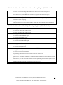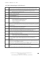
1
U P D A T E
J A N U A R Y
2 8 ,
20 0 2
PCI-HPDI32A-COS
User Manual
Preliminary
General Standards Corporation
8302A Whitesburg Drive
Huntsville, AL 35802
Phone: (256) 880-8787
Fax: (256) 880-8788
URL: www.generalstandards.com
E-mail: [email protected]
User Manual for the PCI-HPDI32A-COS Card, Revision: NR, Manual Revision A
General Standards Corporation
8302A Whitesburg Drive Huntsville, AL 35802, Phone: (256) 880-8787
1
U P D A T E
J A N U A R Y
2 8 ,
20 0 2
User Manual for the PCI-HPDI32A-COS Card, Revision: NR, Manual Revision A
General Standards Corporation
8302A Whitesburg Drive Huntsville, AL 35802, Phone: (256) 880-8787
I
U P D A T E
J A N U A R Y
2 8 ,
20 0 2
PREFACE
General Standards Corporation
Preliminary, Revised: July 20, 2000
Copyright (C) 2000 General Standards Corp.
Additional copies of this manual or other literature may be obtained from:
General Standards Corporation
8302A Whitesburg Dr.
Huntsville, Alabama 35802
Tele: (256) 880-8787
FAX: (256) 880-8788
E-mail: [email protected]
The information in this document is subject to change without notice.
General Standards Corp. makes no warranty of any kind with regard to this material, including, but not limited to,
the implied warranties of merchantability and fitness for a particular purpose. Although extensive editing and
reviews are performed before release to ECO control, General Standards Corp. assumes no responsibility for any
errors that may exist in this document. No commitment is made to update or keep current the information contained
in this document.
General Standards Corp. does not assume any liability arising out of the application or use of any product or
circuit described herein, nor is any license conveyed under any patent rights or any rights of others.
General Standards Corp. assumes no responsibility for any consequences resulting from omissions or errors in this
manual, or from the use of information contained herein.
General Standards Corp. reserves the right to make any changes, without notice, to this product to improve
reliability, performance, function, or design.
All rights reserved
No part of this document may be copied or reproduced in any form or by any means without prior written consent of
General Standards Corp.
This user’s manual provides information on the specifications, theory of operation, register level programming,
installation of the board and information required for customized hardware/software development.
User Manual for the PCI-HPDI32A-COS Card, Revision: NR, Manual Revision: A
General Standards Corporation
8302A Whitesburg Drive Huntsville, AL 35802, Phone: (256) 880-8787
II
U P D A T E
J A N U A R Y
2 8 ,
20 0 2
RELATED PUBLICATIONS
The following manuals and specifications provide the necessary information for in depth understanding of the
specialized parts used on this board.
EIA Standard for the RS-422A Interface (EIA order number EIA -RS-422A)
PCI Local Bus Specification Revision 2.1 June 1, 1995. Questions regarding the PCI specification be forwarded to:
PCI Special Interest Group
P.O. Box 14070
Portland, OR 97214
(800) 433- 5177 (U.S.)
(503) 797-4207 (International)
(503) 234-6762 (FAX)
User Manual for the PCI-HPDI32A-COS Card, Revision: NR, Manual Revision A
General Standards Corporation
8302A Whitesburg Drive Huntsville, AL 35802, Phone: (256) 880-8787
II
U P D A T E
J A N U A R Y
2 8 ,
20 0 2
PCI-HPDI32A-COS Documentation History
1)
2)
November 7, 2001 – Initial Release.
January 28, 2002 – Additions and Error Corrections.
a. Updated board Firmware Revision Error
b. Corrected Error in Register Map Table, Board ID listed in table is incorrect
c. Added Ability to Read Back the Contents of the Event Counter.
d. Clock Divider is 16 Bits, Not 32 Bits
e. Data Mask is 32 Bits, Not 16 Bits.
User Manual for the PCI-HPDI32A-COS Card, Revision: NR, Manual Revision A
General Standards Corporation
8302A Whitesburg Drive Huntsville, AL 35802, Phone: (256) 880-8787
0
U P D A T E
J A N U A R Y
2 8 ,
20 0 2
Table of Contents
1
INTRODUCTION....................................................................................................................................................5
1.1
1.2
1.2.1
1.2.2
1.3
1.4
FUNCTIONAL DESCRIPTION .........................................................................................................................5
THEORY OF OPERATION.................................................................................................................................6
TRANSMITTER OPERATION:..........................................................................................................................................6
RECEIVER OPERATION:................................................................................................................................................7
CABLE INTERFACE...........................................................................................................................................11
FIFOS ........................................................................................................................................................................11
2
REGISTERS ............................................................................................................................................................12
2.1
2.2
2.2.1
2.2.2
2.2.3
2.2.4
2.2.5
2.2.6
2.2.7
2.2.8
2.2.9
2.2.10
2.2.11
2.2.12
2.2.13
2.2.14
2.2.15
2.2.16
2.2.17
2.2.18
2.2.19
2.2.20
2.2.21
2.2.22
2.2.23
2.2.24
PCI-HPDI32A- COS REGISTER INFORMATION ...................................................................................12
PCI-HPDI32A-COS LOCAL REGISTERS, BIT DES CRIPTIONS .......................................................13
FIRMWARE REVISION: (OFFSET 0X00 - RO) – 32 BITS .................................................................................14
BOARD CONTROL: (OFFSET 0 X04 - RW) – 32 BITS ........................................................................................14
BOARD STATUS: (OFFSET 0 X08 - RO) – 32 BITS .............................................................................................15
TX ALMOST: (OFFSET 0X0C - RW) – 32 BITS ....................................................................................................16
RX ALMOST: (OFFSET 0 X10 - RW) – 32 BITS ....................................................................................................17
FIRMWARE FEATURES: (OFFSET 0X14 - RW) – 32 BITS...............................................................................17
RX CLOCK DIVIDER REGISTER: (OFFSET 0 X14 - RW) – 16 BITS . .......................................................................17
FIFO I/O: (OFFSET 0X18 - RW) – 32 BITS ..........................................................................................................17
RX RECEIVE CABLE DATA PORT: (OFFSET 0X1C – RO) – 32 BITS ......................................................................17
RX LOGIC ANALYZER TRIGGER: (OFFSET 0X20 - RW) – 32 BITS .........................................................................18
RX DATA MASK REGISTER: (OFFSET 0X24 - RW) – 32 BITS .................................................................................18
RX EVENT COUNTER REGISTER: (OFFSET 0X28 - RW) – 32 BITS .......................................................................19
RX NUMBER OF WORDS RECEIVED: (OFFSET 0X2C - RO) – 32 BITS .................................................................19
RX EVENT COUNTER REGISTER: (OFFSET 0X0C – R0) – 32 BITS .......................................................................19
INTERRUPT CONTROL: (OFFSET 0 X30 - RW) .................................................................................................20
INTERRUPT STATUS: (OFFSET 0 X34 - RC) ......................................................................................................22
TX CLOCK DIVIDER: (OFFSET 0X38 - RW) ......................................................................................................25
RESERVED: (OFFSET 0X3C - RW) .......................................................................................................................25
TX FIFO SIZE: (OFFSET 0X40 – RO)...................................................................................................................26
RX FIFO SIZE: (OFFSET 0 X44 – RO) ..................................................................................................................26
TX FIFO WORD COUNT: (OFFSET 0 X48 – RO)...............................................................................................26
RX FIFO WORD COUNT: (OFFSET 0 X4C – RO)..............................................................................................26
INTERRUPT EDGE REGISTER: (OFFSET 0X50 – RW)...................................................................................27
INTERRUPT HI/LO REGISTER: (OFFSET 0 X54 – RW) ...................................................................................27
3
PROGRAMMING .................................................................................................................................................28
3.1
3.2
3.3
3.4
INITIALIZATION.................................................................................................................................................28
RESETS ....................................................................................................................................................................28
FIFOS ........................................................................................................................................................................29
INTERRUPTS.........................................................................................................................................................30
4
HARDWARE CONFIGURATION...................................................................................................................31
User Manual for the PCI-HPDI32A-COS Card, Revision: NR, Manual Revision: A
General Standards Corporation
8302A Whitesburg Drive Huntsville, AL 35802, Phone: (256) 880-8787
1
U P D A T E
4.1
4.2
4.3
J A N U A R Y
2 8 ,
20 0 2
THE ON-BOARD TRANSMIT CLOCK ........................................................................................................31
JUMPERS (J5)........................................................................................................................................................32
CABLE CONNECTOR........................................................................................................................................33
Appendix A
PLX REGISTER PROGRAMMING.....................................................................................................34
A.1
CONFIGURATION EEPROM..........................................................................................................................34
A.2
PCI CONFIGURATION REGISTER BIT MAPS .......................................................................................34
A.2.1
PCI C ONFIGURATION ID REGISTER (PCI C ONFIGURATION OFFSET 0X00)........................................................35
A.2.2
PCI C OMMAND REGISTER (PCI C ONFIGURATION OFFSET 0 X04)........................................................................36
A.2.3
PCI S TATUS REGISTER (PCI C ONFIGURATION OFFSET 0X06)..............................................................................37
A.2.4
PCI REVISION ID REGISTER (PCI C ONFIGURATION OFFSET 0X08)....................................................................37
A.2.5
PCI C LASS CODE REGISTER (PCI C ONFIGURATION OFFSET 0 X09..0B) .............................................................38
A.2.6
PCI C ACHE LINE S IZE REGISTER (PCI C ONFIGURATION OFFSET 0 X0C)............................................................38
A.2.7
PCI LATENCY TIMER REGISTER (PCI C ONFIGURATION OFFSET 0X0D)..............................................................38
A.2.8
PCI HEADER TYPE REGISTER (PCI C ONFIGURATION OFFSET 0 X0E)..................................................................38
A.2.9
PCI BUILT-IN S ELF TEST (BIST) REGISTER (PCI C ONFIGURATION OFFSET 0 X0F) ..........................................38
A.2.10
PCI BASE ADDRESS REGISTER FOR MEMORY ACCESS TO RUNTIME REGISTERS (PCI C ONFIGURATION OFFSET
0 X010)
39
A.2.11
PCI BASE ADDRESS REGISTER FOR I/O ACCESS TO RUNTIME REGISTERS (PCI C ONFIGURATION OFFSET
0 X14)
39
A.2.12
PCI BASE ADDRESS REGISTER FOR MEMORY ACCESS TO LOCAL ADDRESS S PACE 0 (PCI C ONFIGURATION
OFFSET 0X18)..................................................................................................................................................................................40
A.2.13
PCI BASE ADDRESS REGISTER FOR MEMORY ACCESS TO LOCAL ADDRESS S PACE 1 (PCI C ONFIGURATION
OFFSET 0X1C) .................................................................................................................................................................................40
A.2.14
PCI BASE ADDRESS REGISTER (PCI C ONFIGURATION OFFSET 0 X20).................................................................40
A.2.15
PCI BASE ADDRESS REGISTER (PCI C ONFIGURATION OFFSET 0 X24).................................................................40
A.2.16
PCI C ARDBUS CIS POINTER REGISTER (PCI C ONFIGURATION OFFSET 0 X28)..................................................40
A.2.17
PCI S UBSYSTEM VENDOR ID REGISTER (PCI C ONFIGURATION OFFSET 0 X2C).................................................41
A.2.18
PCI S UBSYSTEM ID REGISTER (PCI C ONFIGURATION OFFSET 0X2E) ................................................................41
A.2.19
PCI EXPANSION ROM BASE REGISTER (PCI C ONFIGURATION OFFSET 0X30) ..................................................41
A.2.20
PCI INTERRUPT LINE REGISTER (PCI C ONFIGURATION OFFSET 0 X3C) .............................................................41
A.2.21
PCI INTERRUPT PIN REGISTER (PCI C ONFIGURATION OFFSET 0 X3D)...............................................................41
A.2.22
PCI MIN_GNT REGISTER (PCI C ONFIGURATION OFFSET 0X3E).........................................................................41
A.2.23
PCI MAX_LAT REGISTER (PCI C ONFIGURATION OFFSET 0 X3F) .........................................................................41
A.3
LOCAL CONFIGURATION REGISTERS ...................................................................................................42
A.3.1
LOCAL ADDRESS SPACE 0 RANGE REGISTER FOR PCI TO LOCAL BUS (PCI OFFSET 0 X00)..............................43
A.3.2
LOCAL ADDRESS SPACE 0 LOCAL BASE ADDRESS (RE-MAP ) REGISTER FOR PCI TO LOCAL BUS (PCI OFFSET
0 X04)
43
A.3.3
MODE/ARBITRATION REGISTER (PCI OFFSET 0 X08).............................................................................................44
A.3.4
BIG/LITTLE ENDIAN DESCRIPTOR REGISTER (PCI OFFSET 0X0C) .......................................................................45
A.3.5
LOCAL EXPANSION ROM RANGE REGISTER FOR PCI TO LOCAL BUS (PCI OFFSET 0 X10)...............................46
A.3.6
LOCAL EXPANSION ROM LOCAL BASE ADDRESS (RE-MAP) REGISTER FOR PCI TO LOCAL BUS AND BREQO
CONTROL (PCI OFFSET 0X14).......................................................................................................................................................46
A.3.7
LOCAL ADDRESS SPACE 0/EXPANSION ROM BUS REGION DESCRIPTOR REGISTER (PCI OFFSET 0 X18)........46
A.3.8
LOCAL RANGE REGISTER FOR DIRECT MASTER TO PCI (PCI OFFSET 0 X1C) .....................................................47
A.3.9
LOCAL BUS BASE ADDRESS REGISTER FOR DIRECT MASTER TO PCI MEMORY (PCI OFFSET 0 X20) ................47
A.3.10
LOCAL BASE ADDRESS FOR DIRECT MASTER TO PCI IO/CFG REGISTER (PCI OFFSET 0 X24)........................48
A.3.11
PCI BASE ADDRESS (RE-MAP ) REGISTER FOR DIRECT MASTER TO PCI MEMORY (PCI OFFSET 0 X28)...........48
A.3.12
PCI C ONFIGURATION ADDRESS REGISTER FOR DIRECT MASTER TO PCI IO/CFG (PCI OFFSET 0X2C)........49
A.3.13
LOCAL ADDRESS SPACE 1 RANGE REGISTER FOR PCI TO LOCAL BUS (PCI OFFSET 0XF0) .............................49
A.3.14
LOCAL ADDRESS SPACE 1 LOCAL BASE ADDRESS (REMAP) REGISTER (PCI OFFSET 0XF4) .............................50
A.3.15
LOCAL ADDRESS SPACE 1 BUS REGION DESCRIPTOR REGISTER (PCI OFFSET 0XF8) .......................................50
A.4
RUNTIME REGISTERS .....................................................................................................................................51
A.4.1
MAILBOX REGISTER 0 (PCI OFFSET 0X40).............................................................................................................51
User Manual for the PCI-HPDI32A-COS Card, Revision: NR, Manual Revision: A
General Standards Corporation
8302A Whitesburg Drive Huntsville, AL 35802, Phone: (256) 880-8787
2
U P D A T E
J A N U A R Y
2 8 ,
20 0 2
A.4.2
MAILBOX REGISTER 1 (PCI OFFSET 0X44).............................................................................................................51
A.4.3
MAILBOX REGISTER 2 (PCI OFFSET 0X48).............................................................................................................51
A.4.4
MAILBOX REGISTER 3 (PCI OFFSET 0X4C) ............................................................................................................52
A.4.5
MAILBOX REGISTER 4 (PCI OFFSET 0X50).............................................................................................................52
A.4.6
MAILBOX REGISTER 5 (PCI OFFSET 0X54).............................................................................................................52
A.4.7
MAILBOX REGISTER 6 (PCI OFFSET 0X58).............................................................................................................52
A.4.8
MAILBOX REGISTER 7 (PCI OFFSET 0X5C).............................................................................................................52
A.4.9
PCI TO LOCAL DOORBELL REGISTER DESCRIPTION (PCI OFFSET 0X60) ...........................................................52
A.4.10
LOCAL TO PCI DOORBELL REGISTER DESCRIPTION (PCI OFFSET 0X64) ...........................................................52
A.4.11
INTERRUPT CONTROL /S TATUS (PCI OFFSET 0X68)...............................................................................................53
A.4.12
S ERIAL EEPROM C ONTROL, PCI C OMMAND CODES , USER I/O C ONTROL, INIT CONTROL REGISTER (PCI
OFFSET 0X6C) .................................................................................................................................................................................55
A.4.13
PCI PERMANENT CONFIGURATION ID REGISTER (PCI OFFSET 0 X70)...............................................................56
A.4.14
PCI PERMANENT REVISION ID REGISTER (PCI OFFSET 0 X74)............................................................................56
A.5
LOCAL DMA REGISTERS ...............................................................................................................................57
A.5.1
DMA C HANNEL 0 MODE REGISTER (PCI OFFSET 0 X80)......................................................................................57
A.5.2
DMA C HANNEL 0 PCI ADDRESS REGISTER (PCI OFFSET 0 X84).........................................................................58
A.5.3
DMA C HANNEL 0 LOCAL ADDRESS REGISTER (PCI OFFSET 0 X88).....................................................................58
A.5.4
DMA C HANNEL 0 TRANSFER SIZE (BYTES) REGISTER (PCI OFFSET 0 X8C) .......................................................59
A.5.5
DMA C HANNEL 0 DESCRIPTOR POINTER REGISTER (PCI OFFSET 0X90)...........................................................59
A.5.6
DMA C HANNEL 1 MODE REGISTER (PCI OFFSET 0 X94)......................................................................................59
A.5.7
DMA C HANNEL 1 PCI DATA ADDRESS REGISTER (PCI OFFSET 0X98) ..............................................................60
A.5.8
DMA C HANNEL 1 LOCAL DATA ADDRESS REGISTER (PCI OFFSET 0 X9C) .........................................................60
A.5.9
DMA C HANNEL 1 TRANSFER SIZE (BYTES) REGISTER (PCI OFFSET 0 XA0).........................................................60
A.5.10
DMA C HANNEL 1 DESCRIPTOR POINTER REGISTER (PCI OFFSET 0XA4) ..........................................................60
A.5.11
DMA C OMMAND/S TATUS REGISTER (PCI OFFSET 0 XA8).....................................................................................61
A.5.12
DMA C HANNEL 1 C OMMAND /S TATUS REGISTER 0 (PCI OFFSET 0XA8) ............................................................61
A.5.13
DMA ARBITRATION REGISTER 1 (PCI OFFSET 0XAC) ..........................................................................................62
A.5.14
DMA THRESHOLD REGISTER 1 (PCI OFFSET 0 XB0).............................................................................................63
A.6
MESSAGING QUEUE REGISTERS ...............................................................................................................64
A.6.1
OUTBOUND POST LIST FIFO INTERRUPT S TATUS REGISTER (PCI OFFSET 0X30) .............................................64
A.6.2
OUTBOUND POST LIST FIFO INTERRUPT S TATUS REGISTER (PCI OFFSET 0X34) .............................................64
A.6.3
INBOUND QUEUE PORT REGISTER (PCI OFFSET 0X40) ........................................................................................65
A.6.4
OUTBOUND QUEUE PORT REGISTER (PCI OFFSET 0 X44)....................................................................................65
A.6.5
MESSAGING QUEUE CONFIGURATION REGISTER (PCI OFFSET 0XC0)................................................................65
A.6.6
QUEUE BASE ADDRESS REGISTER (PCI OFFSET 0XC4).........................................................................................65
A.6.7
INBOUND FREE HEAD POINTER REGISTER (PCI OFFSET 0XC8) ..........................................................................66
A.6.8
INBOUND FREE HEAD TAIL REGISTER (PCI OFFSET 0 XCC).................................................................................66
A.6.9
INBOUND POST HEAD POINTER REGISTER (PCI OFFSET 0XD0)..........................................................................66
A.6.10
INBOUND POST TAIL POINTER REGISTER (PCI OFFSET 0 XD4).............................................................................66
A.6.11
OUTBOUND FREE HEAD POINTER REGISTER (PCI OFFSET 0 XD8)......................................................................66
A.6.12
OUTBOUND FREE TAIL POINTER REGISTER (PCI OFFSET 0 XDC)........................................................................66
A.6.13
OUTBOUND POST HEAD POINTER REGISTER (PCI OFFSET 0XE0).......................................................................67
A.6.14
OUTBOUND POST TAIL POINTER REGISTER (PCI OFFSET 0XE4).........................................................................67
A.6.15
QUEUE S TATUS /CONTROL REGISTER (PCI OFFSET 0 XE8)....................................................................................67
User Manual for the PCI-HPDI32A-COS Card, Revision: NR, Manual Revision: A
General Standards Corporation
8302A Whitesburg Drive Huntsville, AL 35802, Phone: (256) 880-8787
3
U P D A T E
J A N U A R Y
2 8 ,
20 0 2
Table of Figures
Figure
Figure
Figure
Figure
Figure
Figure
1.1-1 Block Diagram.......................................................................................................................................................... 5
1.2-1 Clock Division Operation........................................................................................................................................ 6
2.2-1 Register Map ........................................................................................................................................................... 13
4.1-1Oscillator Pinout ...................................................................................................................................................... 31
4.2-1 Jumper J5 ................................................................................................................................................................. 32
4.3-1 Cable Pinout ............................................................................................................................................................ 33
Table of Tables
Table 1.2-1 Clock Division Vs Number of Words Loaded into FIFO.................................................................................. 9
Table 4.3-1 Configuration EEPROM Contents........................................................................................................................ 34
Table 4.3-2 Pci Configuration Register Mapping.................................................................................................................... 35
Table 4.3-3 LOCAL CONFIGURATION REGISTERS....................................................................................................... 42
Table 4.3-4 RUN TIME REGISTERS ....................................................................................................................................... 51
Table 4.3-5 DMA REGISTERS .................................................................................................................................................. 57
Table 4.3-6 MESSAGING QUEUE REGISTERS.................................................................................................................. 64
User Manual for the PCI-HPDI32A-COS Card, Revision: NR, Manual Revision: A
General Standards Corporation
8302A Whitesburg Drive Huntsville, AL 35802, Phone: (256) 880-8787
4
U P D A T E
J A N U A R Y
2 8 ,
20 0 2
1 INTRODUCTION
1.1
FUNCTIONAL DESCRIPTION
The PCI-HPDI32A-COS Board includes a DMA Controller, 64/128/256/512 Kbytes of FIFO buffering, a
cable Transmit controller, a cable Receive controller, and cable transceivers (RS-422/485 or differential
pseudo ECL). The DMA on this board is intended for reading and writing the FIFOs. After the DMA is
initialized and started, the host CPU will be free to proceed with other duties and need to respond only to
interrupts. The DMA controller is capable of transferring data to host memory using D32 transfers; whereas
the FIFO memory provides a means for continuous transmission of data without interrupting the DMA or
requiring intervention from the host CPU. The board also provides for DMA chaining, interrupt generation
for various states of the board, including End-Of-Transfer, TX FIFO Almost Empty, RX FIFO Almost Full,
and more. The Transmitter and Receiver are in FPGAs that provide a configurable interface that is highly
flexible in data width and transfer protocol.
Figure 1.1-1 Block Diagram
Tx FIFO
Load
Locctrl
BCR
Start TX
TX
PCI BUS
PLX
BUS
INTERFACE
Cable
Tx Done
BSR
LD0...31
ICR
Start RX
ISR
RX
RX Done
Read
Rx FIFO
User Manual for the PCI-HPDI32A-COS Card, Revision: NR, Manual Revision: A
General Standards Corporation
8302A Whitesburg Drive Huntsville, AL 35802, Phone: (256) 880-8787
5
U P D A T E
1.2
J A N U A R Y
2 8 ,
20 0 2
Theory of Operation
The transmitter and receiver of the standard HPDI32A board have been replaced by a Change of State
Detector and a Logic Analyzer with the following characteristics:
•
•
•
•
•
•
•
20 Mhz Sample rate.
Software Selectable COS or Logic Analyzer Operation.
Software Selectable Clock divider.
Software Selectable COS or Logic Analyzer Mask.
Software Selectable Logic Analyzer Trigger.
Software Programmable Event Counter.
Output data port that can be driven onto the cable on byte wide boundaries.
The Clock Divider is capable of providing a divided down clock enable for operation at slower data rates.
Clock Divider Operation is shown in the following Figure:
Main Clock
Clk Div = 0
Clk Div = 1
Clk Div = 2
Clk Div = 3
Figure 1.2-1 Clock Division Operation
The PCI-HPDI32A-COS board contains 32 programmable I/O Lines that are under software control. The
lines are driven onto the cable on the Cable Data D0 thru Cable Data D31 Lines. Tri-state control on a byte
wide basis is available thru the Board Control Register.
1.2.1
Transmitter Operation:
There is no transmitter on the PCI-HPDI32A -COS Board. There is an Output data register than can be
written by the Host Software. This output data port can be driven onto the data cable with output tri-state
control on a byte wide basis. All 32 data lines can be driven under host control for self test purposes. The
output data lines are synchronized to the Receiver Clock for ease of testing.
1.2.1.1
Tx Data Output Port.
The data output port has replaced the Transmit FIFO. When the Host writes to the Data Output Port, The
data is latched into this register and is available to drive onto the cable. This register can not be read
back.
1.2.1.2
Tx Data Port Output Enable D7-D0. BCR D12
This bit controls the output enable for the Data Port Bits D7-D0. A ‘1’ will enable the board to Drive
Cable Data D7-D0. A ‘0’ will prevent the board from driving Cable Data D7-D0. Default to ‘0’.
User Manual for the PCI-HPDI32A-COS Card, Revision: NR, Manual Revision: A
General Standards Corporation
8302A Whitesburg Drive Huntsville, AL 35802, Phone: (256) 880-8787
6
U P D A T E
J A N U A R Y
2 8 ,
20 0 2
1.2.1.3
Tx Data Port Output Enable D15-D8. BCR D13
This bit controls the output enable for the Data Port Bits D15-D8. A ‘1’ will enable the board to Drive
Cable Data D15-D8. A ‘0’ will prevent the board from driving Cable Data D15-D8. Default to ‘0’.
1.2.1.4
Tx Data Port Output Enable D23-D16. BCR D14
This bit controls the output enable for the Data Port Bits D23-D16. A ‘1’ will enable the board to Drive
Cable Data D23-D16. A ‘0’ will prevent the board from driving Cable Data D23-D16. Default to ‘0’.
1.2.1.5
Tx Data Port Output Enable D31-D24. BCR D15
This bit controls the output enable for the Data Port Bits D31-D24. A ‘1’ will enable the board to Drive
Cable Data D31-D24. A ‘0’ will prevent the board from driving Cable Data D31-D24. Default to ‘0’.
1.2.1.6
Enable Tx – BCR D4
The Transmit Enable bit of the Board Control Register will enable this board to drive all 32 Data Lines.
This bit will over ride the 4 individual output Enables.
1.2.1.7
Start Tx – BCR D8
This bit has been disabled and will do nothing.
1.2.2
Receiver Operation:
The COS Receiver is very flexible with mode bits to control the following Software Selectable options:
•
•
•
•
•
COS or Logic Analyzer Operation.
COS Mask Register – Also Functions as the Logic Analyzer Mask Register.
Software Programmable Event Counter.
Logic Analyzer Trigger Register.
Interrupts available on Software Selectable Options.
o Logic Analyzer Triggered.
o COS Detected.
o FIFO Status Flags.
o Event Counter = 0.
o COS or Logic Analyzer Stopped.
The Receiver will also provide a count of the number of D32 Words received and loaded into the FIFO.
both the COS and Logic Analyzer functions will run until the Receive FIFO status is detected as Almost
Full. The Almost Full flag is programmable under software control.
When the board is running in COS, Change of State, mode it will compare the Masked inputs from the
cable to the Masked results stored in an onboard register. When a difference is detected, the COS Receiver
will store the Changed word into the Receive FIFO, Increment the Number of Words Received Counter,
and Decrement the Event Counter. When the Event Counter has decremented to Zero, This status is
available to the host processor and can be used to generate an interrupt to the host processor. The COS
receiver will continue to collect data until the Receive FIFO becomes Almost Full, or until stopped by the
host processor by removing the Start Receiver bit in the board control register. When stopped by the
Receive FIFO becoming Almost Full, the receiver will generate a Receiver Stopped Status that is readable
thru the Board Status Register and can be used to generate an interrupt to the host processor.
When the board is running in Logic Analyzer mode it will compare the Masked inputs from the Cable to
the Masked Logic Analyzer Trigger Register. If all Masked bits match then the board will enter the LA
Triggered State and Begin collecting data. The Cable data word that generated the Trigger will be the first
word stored into the Receive FIFO. The Logic Analyzer will store every data word on every clock divided
cycle until the FIFO becomes Almost Full or until stopped by the host processor by removing the Enable
Receiver bit in the Board Control Register. When stopped by the Receive FIFO becoming Almost Full, the
receiver will generate a Receiver Stopped Status that is readable thru the Board Status Register and can be
used to generate an interrupt to the host processor.
User Manual for the PCI-HPDI32A-COS Card, Revision: NR, Manual Revision: A
General Standards Corporation
8302A Whitesburg Drive Huntsville, AL 35802, Phone: (256) 880-8787
7
U P D A T E
J A N U A R Y
2 8 ,
20 0 2
1.2.2.1
Rx Command Logic Analyzer Mode. – BCR D16
When this bit is a ‘1’ the board will function in Logic Analyzer mode. When this bit is a ‘0’ then this board
will function in COS mode. `Default is ‘0’.
1.2.2.2
Rx Clock Divider Register – Offset 0x014 – 16 Bits.
The Receive Clock Divider Register has replaced the Firmware Features register used in other boards in the
HPDI32A Family. The receive clock divider will provide a divided down clock enable for COS and Logic
Analyzer operation. A value of Zero will cause full speed board operation at the full Receiver Clock speed,
Typically 20 Mhz. A value of 1 would provide 1 non-Enabled state between Clock Enables. A value of 2
would provide 2 non-Enabled states between clock enables, and so on. See Figure 1.2-1 Clock Division
Operation. In order to access this register using the Standard Windows NT Device Driver you must include
the following Definition in your Source Code.
#define SPL_TX_CLOCK_DIVISION_REG
5
You can then access this register using this register Define.
1.2.2.3
Rx Receive Cable Data Port- Offset 0x01C – 32 Bits – Read Only.
This register will allow the Host processor to read the current state of the Receive Cable Data which is the
data the Receiver has just clocked in from the Data Cable. A Floating Cable will read thru the Rs -422
Transceivers as a logic ‘1’. This register has replaced the Tx Status Block Length Counter.
1.2.2.4
Rx Logic Analyzer Trigger - Offset 0x020 – 32 Bits
The Masked Cable Data will be compared to the Masked contents of this register to determine when to
trigger the Logic Analyzer function. All Masked bits, ‘1’ in the mask, must match for the Logic Analyzer to
Trigger. All non-masked bits in the mask, ‘0’ in the mask, are considered Don’t Cares. A Mask of
0x00000000 is all Don’t cares and will trigger on the First word when the Receiver is started regardless of
the Logic Analyzer Trigger. A mask of 0x0ffffffff will force all 32 bits from the Cable to compare to the 32
bits in the Logic Analyzer Trigger Register. Default is ‘0’ . This register has replaced the Tx Row Valid
Counter.
1.2.2.5
Rx Data Mask Register - Offset 0x024 – 32 Bits
When the board is in COS mode, this Mask Register will be AND’ed bit for bit with the incoming cable
data. Only bits with a ‘1’ in the Mask will be used to determine if a COS has occurred. All bits with a ‘0’ in
the Mask will be ignored while determining COS. The Un-Masked cable Data is what will be loaded into
the FIFO.
When the board is in LA mode, this mask register will be AND’ed bit for bit with the incoming cable data
and the LA Trigger register. The AND’ed results must all match exactly for the LA trigger to occur. All
bits where the mask is ‘1’ will be compared. All bits where the mask is a ‘0’ will be considered ‘Don’t
Cares’ for determining the Trigger Event.
Default is ‘0x0ffffffff’. This register has replaced the Tx Line Invalid Counter.
NOTE: A LA mask of all zero’s will be considered All ‘Don’t Cares’ and will trigger as soon as the
Receiver is started. A COS Mask of all zero’s will ignore all bits and NO COS changes will ever be
detected.
User Manual for the PCI-HPDI32A-COS Card, Revision: NR, Manual Revision: A
General Standards Corporation
8302A Whitesburg Drive Huntsville, AL 35802, Phone: (256) 880-8787
8
U P D A T E
1.2.2.6
J A N U A R Y
2 8 ,
20 0 2
Rx Event Counter Register - Offset 0x028 – 32 Bits
When the Receiver is started in either COS or Logic Analyzer modes then this register will be used to load
a 32 bit down counter. Every time a Change of State is detected using the COS Mask Register then this
counter will be Decre mented. When the Counter reaches Zero the Counter will be halted and the
Rx Event Counter EQ0 status will be sent to the Board Status and Interrupt Control Registers. The Interrupt
Control Register can be used to generate an interrupt if enabled by the host processor. Reading this
location will read the contents of the Register, NOT the contents of the Counter. Default is ‘’0’. This
Counter has replaced the Rx Status Block Length Counter.
The Ability to Read back the Counter has been added with FW Revis ion 01. The Actual Value in the
counter can be read back thru Register Offset 0x0C, which was the TX FIFO ALMOST FLAGS.
NOTE: This counter will still count Change of States even if the board is collecting data in Logic Analyzer
mode.
1.2.2.7
Rx Number of Words Received - Offset 0x02C – 32 Bits – Read Only
When the Receiver is started in either COS or Logic Analyzer modes then this counter will be reset to ‘0’.
Every time a word is loaded into the Receive FIFO then this counter will be incremented. Default is ‘’0’.
This counter is also known as the Rx Row Length Counter.
1.2.2.8
Rx Receiver Stopped Operation Notes.
When the Receiver is running in either COS or LA modes and the Receive FIFO goes Almost Full then all
data collection will Stop and the Receiver will enter the Receiver Stopped state. Due to Timing Delays
from the FIFO, Thru the FPGA, and Back to the FIFO again, the Receiver is not able to Stop Instantly.
When the board is operating at high speed this will cause extra words to be loaded into the FIFO. This is
most noticeable in Logic Analyzer mode, so this discussion will deal with Stopping when in Logic
Analyzer Mode.
It takes 2 clock cycles for the Receiver to Actually shut down when running at full speed. When the Clock
Division register is 0x0000, 2 ext ra words will be loaded into the FIFO. When the Clock Division register
is 0x0001, 1 extra word will be loaded into the FIFO. When the Clock Division Register is 0x02 or higher
then no extra words will be loaded into the Receive FIFO. The extra words will be counted in the Number
of Words Received Counter.
For Example: If the Default FIFO Almost Full setting of 0x08 is used with the Default FIFO’s, 32Kbytes
(0x08000) in Depth,
Table 1.2-1 Clock Division Vs Number of Words Loaded into FIFO
Clock Division
0
1
2
3
All other Values
Number of Words Loaded into
Receive FIFO
0x07ffa
0x07ff9
0x07ff8
0x07ff8
0x07ff8
When the Board is operating in COS, Change of State, mode the same conditions apply, but the receiver
will only try to load data into the FIFO if a Change of State were detected during the 2 clock cycle
shutdown time. The Number of Words Received Counter will always contain the correct value and should
be checked if the board has to Stop because the FIFO has become Almost Full.
User Manual for the PCI-HPDI32A-COS Card, Revision: NR, Manual Revision: A
General Standards Corporation
8302A Whitesburg Drive Huntsville, AL 35802, Phone: (256) 880-8787
9
U P D A T E
1.2.2.9
J A N U A R Y
2 8 ,
20 0 2
Rx Event Counter - Offset 0x0C – 32 Bits
When the Receiver is started in either COS or Logic Analyzer modes then this register will be used to load
a 32 bit down counter. Every time a Change of State is detected using the COS Mask Register then this
counter will be Decremented. When the Counter reaches Zero the Counter will be halted and the
Rx Event Counter EQ0 status will be sent to the Board Status and Interrupt Control Registers. The Interrupt
Control Register can be used to generate an interrupt if enabled by the host processor. When the counter
has reached Zero, it will remain at Zero until the Receiver is stopped. Reading this location will read the
contents of the Counter, to read the Register that this counter is loaded from, read location 0x028. Default
is ‘’0’. This Counter has replaced the Rx FIFO ALMOST FLAGS.
The Ability to Read back the Counter has been added with FW Revision 01. The Actual Value in the
counter can be read back thru Register Offset 0x0C, which was the TX FIFO ALMOST FLAGS.
NOTE: This counter will still count Change of States even if the board is collecting data in Logic Analyzer
mode.
1.2.2.10
Rx COS Event Detected - BCR D26
The Rx COS Event Detected status bit will be set whenever the Receiver is running and Detects a masked
event that is stored into the FIFO. Once set, this status flag will remain stay set until there is a Write to the
Interrupt Status Register. This status bit can be used to generate Interrupts thru the Interrupt Control
Register and the Interrupt Status Register bit D23.
1.2.2.11
Rx Event Count EQ Zero - BCR D25
The Rx Event Count EQ Zero status bit will be set whenever the Event Counter is Zero. When the Receiver
is not running, then the Event Counter will be continuously loaded from the Contents of the Event Counter
Register. When the Counter is Non Zero, this status bit will be a Zero. When the Counter has been
decremented to Zero, then this status bit will be Active and the Counter will be held at Zero until the
receiver is stopped. Writing to the Interrupt Status Register will not affect this bit. This status bit can be
used to generate Interrupts thru the Interrupt Control Register and the Interrupt Status Register bit D22.
User Manual for the PCI-HPDI32A-COS Card, Revision: NR, Manual Revision: A
General Standards Corporation
8302A Whitesburg Drive Huntsville, AL 35802, Phone: (256) 880-8787
10
U P D A T E
1.3
J A N U A R Y
2 8 ,
20 0 2
CABLE INTERFACE
The cable interface consists of 32 bi-directional Cable Data lines, and 2 control / Status output lines,
Transmitter Driving the Cable and Receiver Running, which can employ either differential I/O RS485/422
compatibility or differential pseudo ECL. Refer to cable pin-out in Figure 4.3-1.
The Cable Command Lines are assigned as follows.
• Transmitter Driving Diphase Data Line Connected to Cable Command 5.
• Receiver Running –
Connected to Cable Command 6.
• 32 I/O Lines Connected to Cable Data 0 thru Cable Data 31.
1.4
FIFOs
The FIFOs on the PCI-HPDI32A-COS are used for buffering the receive data. There are a total of four FIFOs
on the board for receive, the Transmit FIFO’s have been removed from the Board. The Receive FIFO’s
consists of 32 bits of data and 4 status flags. The typical configuration is the –128K board ordering option,
which is 128Kbytes of Receive FIFO. The FIFOs are organized as 32K deep by 32 bits wide. The receive
FIFOs are loaded by the cable receive control logic and read by either the CPU or the DMA. The transmit
FIFOs are have been removed. The 4 status flags that accompany the Receive FIFOs are all active low (‘0’
being TRUE) and are as follows: Empty, Almost Empty, Almost Full, Full. The Almost Empty and the
Almost Full status flags can be programmed by the software to become true at most desired levels.
In addition there are 2 FIFO Event Flags that are part of the FIFO system.
• Rx FIFO Underflow – Read of the Rx FIFO while the FIFO is Empty.
• Rx FIFO Overflow – Write to the Rx FIFO while the Rx FIFO is Full.
The Rx FIFO events are cleared by a Rx FIFO Reset.
User Manual for the PCI-HPDI32A-COS Card, Revision: NR, Manual Revision: A
General Standards Corporation
8302A Whitesburg Drive Huntsville, AL 35802, Phone: (256) 880-8787
11
U P D A T E
J A N U A R Y
2 8 ,
20 0 2
2 REGISTERS
2.1
PCI-HPDI32A- COS REGISTER INFORMATION
The PCI-HPDI32A-COS Card complies with the plug-n-play concept. That is, at the time of power-up, an
attempt will be made by the CPU to set up the board to meet the configuration requirements of the system. In
doing this, the CPU will map the amount of I/O space requested by the PCI-HPDI32A-COS Card and return
the configuration base address into the PCI Configuration Register (Offset 0x18) of this Board. All PCI bus
interface functions are handled by the PLX9080-3 PCI bus interface. For more information regarding the PCI
bus interface, please refer to Appendix A, PLX Register Programming.
User Manual for the PCI-HPDI32A-COS Card, Revision: NR, Manual Revision: A
General Standards Corporation
8302A Whitesburg Drive Huntsville, AL 35802, Phone: (256) 880-8787
12
U P D A T E
2.2
J A N U A R Y
2 8 ,
20 0 2
PCI-HPDI32A-COS LOCAL REGISTERS, BIT DESCRIPTIONS
The PCI-HPDI32A-COS board contains the following registers.
Offset
Address
Size
Access*
0x00
D32
RO
0x04
D32
RW
0x08
D32
RO
0x0C
D32
RW
0x0C
D32
RO
0x10
D32
RW
0x14
D16
RW
0x18
D32
R
0x18
D32
W
0x1C
D32
R0
0x20
D32
RW
0x24
D32
RW
0x28
D32
RW
0x2C
D32
RO
0x30
D32
RW
0x34
D32
RC
0x38
D32
N/A
0x2C
N/A
N/A
0x40
D32
RO
0x44
D32
RO
0x48
D32
RO
0x4c
D32
RO
0x50
D32
R/W
0x54
D32
R/W
Figure 2.2-1 Register Map
Register Name
Firmware Revision
Board Control
Board Status
Tx Progra mmable Almost
Rx Event Counter
Rx Programmable Almost
Rx Clock Divider Register
Rx FIFOs
Tx Output Register
Rx Receive Cable Data Port
Rx Logic Analyzer Trigger
Rx Data Mask Register
Rx Event Counter Register
Rx Number of Words Received
Interrupt Control
Interrupt Status
Tx Clock Divider - Removed
Reserved
Tx FIFO Size
Rx FIFO Size - Removed
Tx FIFO Word Count
Rx FIFO Word Count - Removed
Interrupt Edge Select
Interrupt Hi/Lo Level Select
Value
after Reset
0x00100201
0x00000000
0x0000CCXX
REMOVED
0x00000000
0x00080008
0x0000
EMPTY
0x00000000
0x00000000
0x00000000
0x0ffffffff
0x00000000
0x00000000
0x00000000
0x0000031X
Removed
N/A
0x00000000
Removed
0x00000000
Removed
0x00000000
0xFFFFFFFF
* RO - read only
RW - read/write capability
RC - read clear (a write clears the specified bits)
User Manual for the PCI-HPDI32A-COS Card, Revision: NR, Manual Revision: A
General Standards Corporation
8302A Whitesburg Drive Huntsville, AL 35802, Phone: (256) 880-8787
13
U P D A T E
2.2.1
J A N U A R Y
2 8 ,
20 0 2
FIRMWARE REVISION: (Offset 0x00 - RO) – 32 Bits
This Register is used to determine the version of firmware that is programmed into the board. If the logic is
changed to accommodate a modification for any reason then the value in this register is incremented.
Revision 0x00100201: Original version after debug and final release.
D7..D0
D15..D8
D23..D16
D30..D24
D31
2.2.2
Firmware Revision – FW Revision 01
Board Revision
Currently HPDI32A Revision A
Board Identifier
0x0010 Identifies the HPDI32A-COS
Reserved
Firmware Features Identifier.
Indicates that this board does not contains the Firmware Features Register.
BOARD CONTROL: (Offset 0x04 - RW) – 32 Bits
The Board Control Register is strictly under software control and provides the following functionality’s:
a) Resets the board;
b) Resets the transmit FIFOs;
c) Resets the receive FIFOs;
d) Enables the receive logic;
e) Enables the transmit logic;
f) Mode control for the receiver.
D0
D1
D2
D3
D4
D5
D6
D7
D8
Board Reset
Writing a 1 to this bit will generate a self-timed pulse that
is used to reset the on-board logic and the FIFOs.
There is no need for the software to clear this bit, the bit will clear itself.
Tx FIFO Reset
Writing a 1 to this bit will generate a self-timed pulse that will be
used to reset the Tx FIFOs.
After setting this bit, there should be a minimum of 25 Rx clk periods, or 1 millisecond if the
receivers are turned off, before any local accesses are performed.
There is no need for the software to clear this bit, the bit will clear itself.
Rx FIFO Reset
Writing a 1 to this bit will generate a self-timed pulse that will be
used to reset the Rx FIFOs.
After setting this bit, there should be a minimum of 25 Rx clk periods, or 1 millisecond if the
receivers are turned off, before any local accesses are performed.
There is no need for the software to clear this bit, the bit will clear itself.
Reserved
Enable Tx
Writing a 1 to this bit will enable the transmit logic to drive the cable.
Writing a 0 to this bit will disable the transmit logic from driving the cable.
Start Rx
Writing a 1 to this bit will start the receiver.
Writing a 0 to this bit will stop the receiver.
Rx Disable Output Status Lines
When this bit is set to a ‘0’, then this board will drive Cable Command D5 and D6
When this bit is set to a ‘1’, this board will be prevented from driving Cable Command D5 and D6
Default is ‘0’.
Reserved
Start Tx
Not Used.
User Manual for the PCI-HPDI32A-COS Card, Revision: NR, Manual Revision: A
General Standards Corporation
8302A Whitesburg Drive Huntsville, AL 35802, Phone: (256) 880-8787
14
U P D A T E
D11..D9
D12
D13
D14
D15
D16
D17-D32
2.2.3
J A N U A R Y
2 8 ,
20 0 2
Reserved
Tx Data Port Output Enable D7-D0
A ‘1’ will enable the board to Drive Cable Data D7-D0.
A ‘0’ will prevent the board from driving Cable Data D7-D0.
Default to ‘0’.
Tx Data Port Output Enable D15-D8
A ‘1’ will enable the board to Drive Cable Data D15-D8.
A ‘0’ will prevent the board from driving Cable Data D15-D8.
Default to ‘0’.
Tx Data Port Output Enable D23-D16
A ‘1’ will enable the board to Drive Cable Data D23-D16.
A ‘0’ will prevent the board from driving Cable Data D23-D16.
Default to ‘0’.
Tx Data Port Output Enable D31-D24
A ‘1’ will enable the board to Drive Cable Data D31-D24.
A ‘0’ will prevent the board from driving Cable Data D31-D24.
Default to ‘0’.
Rx Command Logic Analyzer Mode.
Writing a 1 to this bit will enable Receiving Data in Logic Analyzer Mode.
Writing a 0 to this bit will enable Receiving Data in COS, Change of State Mode.
Default is ‘0’, Change of State Mode.
Reserved.
BOARD STATUS: (Offset 0x08 - RO) – 32 Bits
The Board Status Register is used to return information to the software about the most current status of the
board, at the time of the reading. Listed below is the information that this register contains:
D0
D1
D2
D3
D4
D5
D6
D7
D8
D9
D10
D11
D12
D13
D14
Rx Cable Command D0
Rx Cable Command D1.
Rx Cable Command D2
Rx Cable Command D3.
Rx Cable Command D4.
Rx Cable Command D5.
Rx Cable Command D6.
Tx Transmit Done.
Not Used
Tx FIFO Empty L
Not Used
Tx FIFO Almost Empty L
Not Used
Tx FIFO Almost Full L
Not Used
Tx FIFO Full L
Not Used
Rx FIFO Empty L
1 will indicate the Rx FIFO is not empty.
0 will indicate the Rx FIFO is empty.
Rx FIFO Almost Empty L
1 will indicate the Rx FIFO is not almost empty.
0 will indicate the Rx FIFO is empty.
Rx FIFO Almost Full L
1 will indicate the Rx FIFO is not almost full.
0 will indicate the Rx FIFO is almost full.
User Manual for the PCI-HPDI32A-COS Card, Revision: NR, Manual Revision: A
General Standards Corporation
8302A Whitesburg Drive Huntsville, AL 35802, Phone: (256) 880-8787
15
U P D A T E
D15
D16
D17
D18
D19
D20
D21
D22
D23
D24
D25
D26
D31..D27
2.2.4
J A N U A R Y
2 8 ,
20 0 2
Rx FIFO Full L
1 will indicate the Rx FIFO is not full.
0 will indicate the Rx FIFO is full.
Board Jumper 0
1 will indicate that Board Jumper 0 is present
0 will indicate that board jumper 0 is absent
Board Jumper 1
1 will indicate that Board Jumper 1 is present
0 will indicate that board jumper 1 is absent
Reserved
Rx FIFO Underflow.
1 will indicate that a Receive FIFO underflow has occurred
0 will indicate that no Receive FIFO underflow has occurred
Rx FIFO Overflow.
1 will indicate that a Receive FIFO overflow has occurred
0 will indicate that no Receive FIFO overflow has occurred
Tx FIFO Overflow.
Not Used
Rx Receive Stopped
1 will indicate that the Receiver FIFO has become Almost Full and the Receiver has Stopped.
0 will indicate that the Receiver is not running, or is busy receiving data.
Rx Logic Analyzer Triggered.
1 will indicate that the Receiver is currently in Logic Analyzer mode and has detected the Trigger.
0 will indicate that the Receiver is not currently receiving a Logic Analyzer message.
Rx Receive Running
1 will indicate that the Receiver has been started and is not Receive Stopped.
0 will indicate that the Receiver has not been started, or has been started but is now Stopped.
Rx Event Counter EQ Zero
1 will indicate the Receive Event Counter has Decremented to Zero.
0 will indicate the Receive Event Counter has not decremented to zero. .
Rx COS Event Detected
1 will indicate the Receiver has just now detected a COS event. .
0 will indicate the Receiver is not now detecting a COS event.
This bit will be set and cleared many times during the collection of data.
Reserved
TX ALMOST: (Offset 0x0C - RW) – 32 Bits
This register is contains the values that are used to program the Almost Flags of the transmit FIFOs.
This register is not used on the COS board. The Transmit FIFO’s have been removed.
Default is 0x00080008.
Almost Empty = 0x0008
Almost Full = 0x0008 from full.
D7..D0
D15..D8
D23..D16
D31..D24
Low byte, Almost Empty
High byte, Almost Empty
Low byte, Almost Full
High byte, Almost Full
User Manual for the PCI-HPDI32A-COS Card, Revision: NR, Manual Revision: A
General Standards Corporation
8302A Whitesburg Drive Huntsville, AL 35802, Phone: (256) 880-8787
16
U P D A T E
2.2.5
J A N U A R Y
2 8 ,
20 0 2
RX ALMOST: (Offset 0x10 - RW) – 32 Bits
This register is contains the values that are used to program the Almost Flags of the receive FIFOs.
Default is 0x00080008.
Almost Empty = 0x0008
Almost Full = 0x0008 from full.
D7..D0
D15..D8
D23..D16
D31..D24
2.2.6
Low byte, Almost Empty
High byte, Almost Empty
Low byte, Almost Full
High byte, Almost Full
FIRMWARE FEATURES: (Offset 0x14 - RW) – 32 Bits
Register to note new features present in FW. This Register has been removed from the COS.
2.2.7
Rx Clock Divider Register: (Offset 0x14 - RW) – 16 Bits.
The Receive Clock Divider Register has replaced the Firmware Features register used in other boards in the
HPDI32A Family. The receive clock divider will provide a divided down clock enable for COS and Logic
Analyzer operation. A value of Zero will cause full speed board operation at the full Receiver Clock speed,
Typically 20 Mhz. A value of 1 would provide 1 non-Enabled state between Clock Enables. A value of 2
would provide 2 non-Enabled states between clock enables, and so on. See Figure 1.2-1 Clock Division
Operation. In order to access this register using the Standard Windows NT Device Driver you must include
the following Definition in your Source Code.
#define SPL_TX_CLOCK_DIVISION_REG
5
You can then access this register using this register Define.
D15..D0
D31..D16
2.2.8
Rx Clock Divider Register
Not Used
FIFO I/O: (Offset 0x18 - RW) – 32 Bits
The 64/128/256/ Kbytes FIFOs are used for buffering Receive data. This gives the software a means of
buffering the data before it is sent over the PCI bus. The FIFOs are also used by the DMA for the same
purpose. This eliminates unnecessary PCI bus arbitration which provides for faster and more efficient bus
cycles for transfers; hence, a faster and more efficient system. Typical configuration is 128Kbytes which is
128Kbytes Receive FIFO (32 K by 32 bits) . The Transmit FIFO has been removed from the COS board.
D31..D0
2.2.9
FIFO Data 0..31
This is the buffer that contains both the transmit and receive data.
A write to this offset will load into the Tx Data Output Port.
A read from this offset will read from the Receive FIFO.
Rx Receive Cable Data Port: (Offset 0x1C – RO) – 32 Bits
This register will allow the Host processor to read the current state of the Receive Cable Data which is the
data the Receiver has just clocked in from the Data Cable. A Floating Cable will read thru the Rs-422
Transceivers as a logic ‘1’. This register has replaced the Tx Status Block Length Counter.
D31..D0
Data 0..31
The current state of the Receive Cable Data D31..D0.
User Manual for the PCI-HPDI32A-COS Card, Revision: NR, Manual Revision: A
General Standards Corporation
8302A Whitesburg Drive Huntsville, AL 35802, Phone: (256) 880-8787
17
U P D A T E
J A N U A R Y
2 8 ,
20 0 2
2.2.10 Rx Logic Analyzer Trigger: (Offset 0x20 - RW) – 32 Bits
The Masked Cable Data will be compared to the Masked contents of this register to determine when to
trigger the Logic Analyzer function. All Masked bits, ‘1’ in the mask, must match for the Logic Analyzer to
Trigger. All non-masked bits in the mask, ‘0’ in the mask, are considered Don’t Cares. A Mask of
0x00000000 is all Don’t cares and will trigger on the First word when the Receiver is started regardless of
the Logic Analyzer Trigger. A mask of 0x0ffffffff will force all 32 bits from the Cable to compare to the 32
bits in the Logic Analyzer Trigger Register. Default is ‘0’ . This register has replaced the Tx Row Valid
Counter.
D31..D0
Data 0..31
The Logic Analyzer Trigger Word
2.2.11 Rx Data Mask Register: (Offset 0x24 - RW) – 32 Bits.
When the board is in COS mode, this Mask Register will be AND’ed bit for bit with the incoming cable
data. Only bits with a ‘1’ in the Mask will be used to determine if a COS has occurred. All bits with a ‘0’ in
the Mask will be ignored while determining COS. The Un-Masked cable Data is what will be loaded into
the FIFO.
When the board is in LA mode, this mask register will be AND’ed bit for bit with the incoming cable data
and the LA Trigger register. The AND’ed results must all match exactly for the LA trigger to occur. All
bits where the mask is ‘1’ will be compared. All bits where the mask is a ‘0’ will be considered ‘Don’t
Cares’ for determining the Trigger Event.
Default is ‘0x0ffffffff’. This register has replaced the Tx Line Invalid Counter.
D31..D0
Data 0..31
The COS and Logic Analyzer Data Mask. .
NOTE: A LA mask of all zero’s will be considered All ‘Don’t Cares’ and will trigger as soon as the
Receiver is started. A COS Mask of all zero’s will ignore all bits and NO COS changes will ever be
detected.
User Manual for the PCI-HPDI32A-COS Card, Revision: NR, Manual Revision: A
General Standards Corporation
8302A Whitesburg Drive Huntsville, AL 35802, Phone: (256) 880-8787
18
U P D A T E
J A N U A R Y
2 8 ,
20 0 2
2.2.12 Rx Event Counter Register: (Offset 0x28 - RW) – 32 Bits
When the Receiver is started in either COS or Logic Analyzer modes then this register will be used to load
a 32 bit down counter. Every time a Change of State is detected using the COS Mask Register then this
counter will be Decremented. When the Counter reaches Zero the Counter will be halted and the
Rx Event Counter EQ0 status will be sent to the Board Status and Interrupt Control Registers. The Interrupt
Control Register can be used to generate an interrupt if enabled by the host processor. Reading this
location will read the contents of the Register, NOT the contents of the Counter. Default is ‘’0’. This
Counter has replaced the Rx Status Block Length Counter.
NOTE: This counter will still count Change of States even if the board is collecting data in Logic Analyzer
mode..
D31..D0
Rx Event Counter Register.
Decremented to Zero with each COS event detected.
2.2.13 Rx Number of Words Received: (Offset 0x2C - RO) – 32 Bits
When the Receiver is started in either COS or Logic Analyzer modes then this counter will be reset to ‘0’.
Every time a word is loaded into the Receive FIFO then this counter will be incremented. Default is ‘’0’.
This counter is also known as the Rx Row Length Counter. The Host Processor can read it at any time.
D31..D0
Counter 0..31
The number of D32 Words received in this message.
It is reset to 0 when the Receiver is started.
2.2.14 Rx Event Counter Register: (Offset 0x0C – R0) – 32 Bits
This Counter has been added with Firmware Revision A, ( 01 ). Reading this location will give the Current
contents of the Event Counter. When the Counter has Decremented to Zero it will be held at zero until the
Receiver is stopped. When the Receiver is Stopped, This Counter will be continuously loaded from the
contents of the Rx Event Counter Register. This Counter is Read Only.
D31..D0
Rx Event Counter.
Decremented to Zero with each COS event detected.
User Manual for the PCI-HPDI32A-COS Card, Revision: NR, Manual Revision: A
General Standards Corporation
8302A Whitesburg Drive Huntsville, AL 35802, Phone: (256) 880-8787
19
U P D A T E
J A N U A R Y
2 8 ,
20 0 2
2.2.15 INTERRUPT CONTROL: (Offset 0x30 - RW)
The Interrupt Control Register provides the software with a means of selecting what conditions will be
allowed to generate an interrupt.
D0
D1
D2
D3
D4
D5
D6
D7
D8
D9
D10
D11
D12
D13
D14
Enable Interrupt on Cable Command 1 Rising Edge.
1 will allow an interrupt on the Cable Command 1 Lines rising edge.
0 will disallow an interrupt on the Cable Command 1 Lines rising edge.
Enable Interrupt on Cable Command 1 Falling Edge.
1 will allow an interrupt on Cable Command 1 Falling Edge.
0 will disallow an interrupt on Cable Command 1 Falling Edge.
Enable Interrupt on Cable Command 2 a logic ‘1’.
1 will allow an interrupt on Cable Command 2 a logic ‘1’.
0 will disallow an interrupt Cable Command2 a logic ‘1’.
Enable Interrupt on Cable Command 3 a logic ‘1’.
1 will allow an interrupt on Cable Command 3 a logic ‘1’
0 will disallow an interrupt Cable Command 3 a logic ‘1’
Enable Interrupt on Cable Command 4 a logic ‘1’.
1 will allow an interrupt on Cable Command 4 a logic ‘1’
0 will disallow an interrupt Cable Command 4 a logic ‘1’
Enable Interrupt on Cable Command 5 a logic ‘1’. – Cable Transmitter Driving the Cable
1 will allow an interrupt on Cable Command 5 a logic ‘1’
0 will disallow an interrupt Cable Command 5 a logic ‘1’
Enable Interrupt on Cable Command 6 a logic ‘1’. – Cable Receiver Ready to Receive
1 will allow an interrupt on Cable Command 6 a logic ‘1’
0 will disallow an interrupt Cable Command 6 a logic ‘1’
Enable Interrupt on Tx Transmit Done. – Not Used.
1 will allow an interrupt on Tx Transmit Done.
0 will disallow an interrupt on Tx Transmit Done.
Enable Interrupt on Tx FIFO Empty. – Not Used.
1 will allow an interrupt on Tx FIFO empty.
0 will disallow an interrupt on Tx FIFO empty.
Enable Interrupt on Tx FIFO Almost Empty. – Not Used.
1 will allow an interrupt on Tx FIFO almost empty.
0 will disallow an interrupt on Tx FIFO almost empty.
Enable Interrupt on Tx FIFO Almost Full. – Not Used.
1 will allow an interrupt on Tx FIFO almost full.
0 will disallow an interrupt on Tx FIFO almost full.
Enable Interrupt on Tx FIFO Full. – Not Used.
1 will allow an interrupt on Tx FIFO full.
0 will disallow an interrupt on Tx FIFO full.
Enable Interrupt on Rx FIFO NOT Empty
1 will allow an interrupt on Rx FIFO NOT empty.
0 will disallow an interrupt on Rx FIFO NOT empty.
Enable Interrupt on Rx FIFO NOT Almost Empty
1 will allow an interrupt on Rx FIFO NOT Almost empty.
0 will disallow an interrupt on Rx FIFO NOT Almost empty.
Enable Interrupt on Rx FIFO Almost Full
1 will allow an interrupt on Rx FIFO almost full.
0 will disallow an interrupt on Rx FIFO almost full.
User Manual for the PCI-HPDI32A-COS Card, Revision: NR, Manual Revision: A
General Standards Corporation
8302A Whitesburg Drive Huntsville, AL 35802, Phone: (256) 880-8787
20
U P D A T E
D15
D16
D17
D18
D19
D20
D21
D22
D23
D31..24
J A N U A R Y
2 8 ,
20 0 2
Enable Interrupt on Rx FIFO Full
1 will allow an interrupt on Rx FIFO full.
0 will disallow an interrupt on Rx FIFO full.
Enable Interrupt on Rx FIFO Underflow.
1 will allow an interrupt on Rx FIFO Underflow.
0 will disallow an interrupt on Rx FIFO Underflow.
Enable Interrupt on Rx FIFO Overflow.
1 will allow an interrupt on Rx FIFO Overflow.
0 will disallow an interrupt on Rx FIFO Overflow.
Enable Interrupt on Tx FIFO Overflow. – Not Used.
1 will allow an interrupt on Tx FIFO Overflow.
0 will disallow an interrupt on Tx FIFO Overflow.
Enable Interrupt on Rx Receive Stopped.
1 will allow an interrupt on Rx Receive Stopped.
0 will disallow an interrupt on Rx Receive Stopped.
Enable Interrupt on Rx Logic Analyzer Triggered.
1 will allow an interrupt on Rx Logic Analyzer Triggered.
0 will disallow an interrupt on Rx Logic Analyzer Triggered.
Enable Interrupt on Rx Receive Running.
1 will allow an interrupt on Rx Receive Running.
0 will disallow an interrupt on Rx Receive Running.
Enable Interrupt on Rx Event Counter EQ Zero.
1 will allow an interrupt on Rx Event Counter EQ Zero.
0 will disallow an interrupt on Rx Event Counter EQ Zero.
Enable Interrupt on Rx COS Event Detected.
1 will allow an interrupt on Rx COS Event Detected.
0 will disallow an interrupt on Rx COS Event Detected.
Reserved
User Manual for the PCI-HPDI32A-COS Card, Revision: NR, Manual Revision: A
General Standards Corporation
8302A Whitesburg Drive Huntsville, AL 35802, Phone: (256) 880-8787
21
U P D A T E
J A N U A R Y
2 8 ,
20 0 2
2.2.16 INTERRUPT STATUS: (Offset 0x34 - RC)
The Interrupt Status Register serves as a dual-purpose register. Each bit in this register operates
independently of each other. If an interrupt condition is enabled, in the Interrupt Control Register, the
appropriate bit, in the Interrupt Status Register, will indicate if an interrupt has occurred or not, and it will
continue to indicate this until the software resets that bit. If an interrupt bit is not enabled, in the Interrupt
Control Register, then the appropriate bit, in the Interrupt Status Register, will indicate whether or not the
condition exists for an interrupt request.
D0
D1
D2
D3
D4
Cable Command 1Rising Edge
If this bit is enabled as an interrupt
a 1 will indicate that an interrupt on the Cable Command 1Rising Edge has occurred.
a 0 will indicate that an interrupt on the Cable Command 1Rising Edge has not occurred.
If this bit is not enabled as an interrupt
a 1 will indicate that the Cable Command 1 is a Rising Edge now.
a 0 will indicate that the Cable Command 1 is not a rising edge.
Cable Command 1 Falling Edge
If this bit is enabled as an interrupt
a 1 will indicate that an interrupt on the Cable Command 1 Falling Edge has occurred.
a 0 will indicate that an interrupt on the Cable Command 1 Falling Edge has not occurred.
If this bit is not enabled as an interrupt
a 1 will indicate that the Cable Command 1 is a Falling Edge now.
a 0 will indicate that the Cable Command 1 is not a Falling edge.
Cable Command 2
If this bit is enabled as an interrupt
a 1 will indicate that an interrupt on Cable Command 2 has occurred.
a 0 will indicate that an interrupt on Cable Command 2 has not occurred.
If this bit is not enabled as an interrupt
a 1 will indicate that Cable Command 2 is currently a ‘1’.
a 0 will indicate that Cable Command 2 is not currently a ‘1’.
Cable Command 3
If this bit is enabled as an interrupt
a 1 will indicate that an interrupt on Command 3 has occurred.
a 0 will indicate that an interrupt on Command 3 has not occurred.
If this bit is not enabled as an interrupt
a 1 will indicate that Cable Command 3 is currently a ‘1’.
a 0 will indicate that Cable Command 3 is not currently a ‘1’.
Cable Command 4
If this bit is enabled as an interrupt
a 1 will indicate that an interrupt on Cable Command 4 has occurred.
a 0 will indicate that an interrupt on Cable Command 4 has not occurred.
If this bit is not enabled as an interrupt
a 1 will indicate that Cable Command 4 is currently a ‘1’
a 0 will indicate that Cable Command 4 is not currently a ‘1’.
User Manual for the PCI-HPDI32A-COS Card, Revision: NR, Manual Revision: A
General Standards Corporation
8302A Whitesburg Drive Huntsville, AL 35802, Phone: (256) 880-8787
22
U P D A T E
D5
D6
D7
D8
D9
D10
D11
J A N U A R Y
2 8 ,
20 0 2
Cable Command 5 - Cable Transmitter Driving the Cable
If this bit is enabled as an interrupt
a 1 will indicate that an interrupt on Cable Command 5 has occurred.
a 0 will indicate that an interrupt on Cable Command 5 has not occurred.
If this bit is not enabled as an interrupt
a 1 will indicate that Cable Command 5 is currently a ‘1’
a 0 will indicate that Cable Command 5 is not currently a ‘1’.
Cable Command 6 – Cable Receiver Ready to Receive
If this bit is enabled as an interrupt
a 1 will indicate that an interrupt on Cable Command 6 has occurred.
a 0 will indicate that an interrupt on Cable Command 6 has not occurred.
If this bit is not enabled as an interrupt
a 1 will indicate that Cable Command 6 is currently a ‘1’
a 0 will indicate that Cable Command 6 is not currently a ‘1’.
Tx Transmit Done. – Not Used
If this bit is enabled as an interrupt
a 1 will indicate that an interrupt on Tx Transmit Done has occurred.
a 0 will indicate that an interrupt on Tx Transmit Done has not occurred.
If this bit is not enabled as an interrupt
a 1 will indicate that Tx Transmit Done has occurred.
a 0 will indicate that Tx Transmit Done has not occurred.
Tx FIFO Empty. – Not Used
If this bit is enabled as an interrupt
a 1 will indicate that an interrupt on the Tx FIFO empty has occurred.
a 0 will indicate that an interrupt on the Tx FIFO empty has not occurred.
If this bit is not enabled as an interrupt
a 1 will indicate that the Tx FIFO is currently empty
a 0 will indicate that the Tx FIFO is not currently empty.
Tx FIFO Almost Empty. – Not Used
If this bit is enabled as an interrupt
a 1 will indicate that an interrupt on the Tx FIFO almost empty has occurred.
a 0 will indicate that an interrupt on the Tx FIFO almost empty has not occurred.
If this bit is not enabled as an interrupt
a 1 will indicate that the Tx FIFO is currently almost empty.
a 0 will indicate that the Tx FIFO is not currently almost empty.
Tx FIFO Almost Full. – Not Used
If this bit is enabled as an interrupt
a 1 will indicate that an interrupt on the Tx FIFO almost full has occurred.
a 0 will indicate that an interrupt on the Tx FIFO almost full has not occurred.
If this bit is not enabled as an interrupt
a 1 will indicate that the Tx FIFO is currently almost full.
a 0 will indicate that the Tx FIFO is not currently almost full.
Tx FIFO Full. – Not Used
If this bit is enabled as an interrupt
a 1 will indicate that an interrupt on the Tx FIFO full has occurred.
a 0 will indicate that an interrupt on the Tx FIFO full has not occurred.
If this bit is not enabled as an interrupt
a 1 will indicate that the Tx FIFO is currently full.
a 0 will indicate that the Tx FIFO is not currently full.
User Manual for the PCI-HPDI32A-COS Card, Revision: NR, Manual Revision: A
General Standards Corporation
8302A Whitesburg Drive Huntsville, AL 35802, Phone: (256) 880-8787
23
U P D A T E
D12
D13
D14
D15
D16
D17
D18
J A N U A R Y
2 8 ,
20 0 2
Rx FIFO Empty
If this bit is enabled as an interrupt
a 1 will indicate that an interrupt on the Rx FIFO empty has occurred.
a 0 will indicate that an interrupt on the Rx FIFO empty has not occurred.
If this bit is not enabled as an interrupt
a 1 will indicate that the Rx FIFO is currently empty
a 0 will indicate that the Rx FIFO is not currently empty.
Rx FIFO Almost Empty
If this bit is enabled as an interrupt
a 1 will indicate that an interrupt on the Rx FIFO almost empty has occurred.
a 0 will indicate that an interrupt on the Rx FIFO almost empty has not occurred.
If this bit is not enabled as an interrupt
a 1 will indicate that the Rx FIFO is currently almost empty.
a 0 will indicate that the Rx FIFO is not currently almost empty.
Rx FIFO Almost Full
If this bit is enabled as an interrupt
a 1 will indicate that an interrupt on the Rx FIFO almost full has occurred.
a 0 will indicate that an interrupt on the Rx FIFO almost full has not occurred.
If this bit is not enabled as an interrupt
a 1 will indicate that the Rx FIFO is currently almost full.
a 0 will indicate that the Rx FIFO is not currently almost full.
Rx FIFO Full
If this bit is enabled as an interrupt
a 1 will indicate that an interrupt on the Rx FIFO full has occurred.
a 0 will indicate that an interrupt on the Rx FIFO full has not occurred.
If this bit is not enabled as an interrupt
a 1 will indicate that the Rx FIFO is currently full.
a 0 will indicate that the Rx FIFO is not currently full.
Enable Interrupt on Rx FIFO Underflow.
If this bit is enabled as an interrupt
a 1 will indicate that an interrupt on Rx FIFO Underflow has occurred.
a 0 will indicate that an interrupt on Rx FIFO Underflow has not occurred.
If this bit is not enabled as an interrupt
a 1 will indicate that Rx FIFO Underflow has occurred.
a 0 will indicate that Rx FIFO Underflow is not occurred.
Enable Interrupt on Rx FIFO Overflow.
If this bit is enabled as an interrupt
a 1 will indicate that an interrupt on Rx FIFO Overflow has occurred.
a 0 will indicate that an interrupt on Rx FIFO Overflow has not occurred.
If this bit is not enabled as an interrupt
a 1 will indicate that Rx FIFO Overflow has occurred.
a 0 will indicate that Rx FIFO Overflow has not occurred.
Enable Interrupt on Tx FIFO Overflow. – Not Used
If this bit is enabled as an interrupt
a 1 will indicate that an interrupt on Tx FIFO Overflow has occurred.
a 0 will indicate that an interrupt on Tx FIFO Overflow has not occurred.
If this bit is not enabled as an interrupt
a 1 will indicate that a Tx FIFO Overflow has occurred.
a 0 will indicate that a Tx FIFO Overflow has not occurred.
User Manual for the PCI-HPDI32A-COS Card, Revision: NR, Manual Revision: A
General Standards Corporation
8302A Whitesburg Drive Huntsville, AL 35802, Phone: (256) 880-8787
24
U P D A T E
D19
D20
D21
D22
D23
D31..21
J A N U A R Y
2 8 ,
20 0 2
Enable Interrupt on Rx Receive Stopped.
If this bit is enabled as an interrupt
a 1 will indicate that an interrupt Rx Receive Stopped has occurred.
a 0 will indicate that an interrupt Rx Receive Stopped has not occurred.
If this bit is not enabled as an interrupt
a 1 will indicate that a Rx Receive Stopped has occurred.
a 0 will indicate that a Rx Receive Stopped has not occurred.
Enable Interrupt on Rx Logic Analyzer Triggered.
If this bit is enabled as an interrupt
a 1 will indicate that an interrupt on Rx Logic Analyzer Triggered has occurred.
a 0 will indicate that an interrupt on Rx Logic Analyzer Triggered has not occurred.
If this bit is not enabled as an interrupt
a 1 will indicate that Rx Logic Analyzer Triggered has occurred.
a 0 will indicate that Rx Logic Analyzer Triggered has not occurred
Enable Interrupt on Rx Receive Running.
If this bit is enabled as an interrupt
a 1 will indicate that an interrupt on Rx Receive Running has occurred.
a 0 will indicate that an interrupt on Rx Receive Running has not occurred.
If this bit is not enabled as an interrupt
a 1 will indicate that Rx Receive Running has occurred.
a 0 will indicate that Rx Receive Running has not occurred
Enable Interrupt on Rx Event Counter EQ Zero.
If this bit is enabled as an interrupt
a 1 will indicate that an interrupt on Rx Event Counter EQ Zero has occurred.
a 0 will indicate that an interrupt on Rx Event Counter EQ Zero sy has not occurred.
If this bit is not enabled as an interrupt
a 1 will indicate that Rx Event Counter EQ Zero has occurred.
a 0 will indicate that Rx Event Counter EQ Zero has not occurred
Enable Interrupt on Rx COS Event Detected.
If this bit is enabled as an interrupt
a 1 will indicate that an interrupt on Rx COS Event Detected has occurred.
a 0 will indicate that an interrupt on Rx COS Event Detected has not occurred.
If this bit is not enabled as an interrupt
a 1 will indicate that Rx COS Event Detected has occurred.
a 0 will indicate that Rx COS Event Detected has not occurred
Reserved
2.2.17 TX CLOCK DIVIDER: (Offset 0x38 - RW)
This Transmit Clock Divider has been removed from the PCI-HPDI32A-COS.
This function, the Rx Clock Divider is accessed thru Register 0x014 .
NOTE: This register cannot be accessed using the currently released Windows NT Device Driver.
2.2.18 RESERVED: (Offset 0x3C - RW)
This register is reserved for future use.
NOTE: This register cannot be accessed using the currently released Windows NT Device Driver.
User Manual for the PCI-HPDI32A-COS Card, Revision: NR, Manual Revision: A
General Standards Corporation
8302A Whitesburg Drive Huntsville, AL 35802, Phone: (256) 880-8787
25
U P D A T E
J A N U A R Y
2 8 ,
20 0 2
2.2.19 TX FIFO SIZE: (Offset 0x40 – RO)
This feature has been removed from the PCI-HPDI32A-COS.
NOTE: This register cannot be accessed using the currently released Windows NT Device Driver.
D19..D0
D31..D20
Reserved
Undefined
2.2.20 RX FIFO SIZE: (Offset 0x44 – RO)
This feature has been removed from the PCI-HPDI32A-COS.
NOTE: This register cannot be accessed using the currently released Windows NT Device Driver.
D19..D0
D31..D20
Reserved.
Undefined
2.2.21 TX FIFO WORD COUNT: (Offset 0x48 – RO)
This feature has been removed from the PCI-HPDI32A-COS.
NOTE: This register cannot be accessed using the currently released Windows NT Device Driver.
D19..D0
D31..D20
Reserved
Undefined
2.2.22 RX FIFO WORD COUNT: (Offset 0x4C – RO)
This feature has been removed from the PCI-HPDI32A-COS.
NOTE: This register cannot be accessed using the currently released Windows NT Device Driver.
D19..D0
D31..D20
Reserved.
Undefined
User Manual for the PCI-HPDI32A-COS Card, Revision: NR, Manual Revision: A
General Standards Corporation
8302A Whitesburg Drive Huntsville, AL 35802, Phone: (256) 880-8787
26
U P D A T E
J A N U A R Y
2 8 ,
20 0 2
2.2.23 INTERRUPT EDGE REGISTER: (Offset 0x50 – RW)
Thirty-two bit register to define interrupt source to individually define as edge or level sensitive. Bits are
the same order as the interrupt source. Default is 0, Level Triggered Interrupts to maintain compatibility
with existing devices.
NOTE: This register cannot be accessed using the currently released Windows NT Device Driver.
D31..D0
Interrupt Edge Select
Individual Interrupt level or edge trigger select.
0 = Level Triggered Interrupts.
1 = Edge Triggered Interrupts.
2.2.24 INTERRUPT HI/LO REGISTER: (Offset 0x54 – RW)
Thirty-two bit register to define interrupt source as active hi or active lo. Bits are in same order as interrupt
source. Default is 1, Active High Interrupts to maintain compatibility with existing devices.
NOTE: This register cannot be accessed using the currently released Windows NT Device Driver.
.
D31..D0
Interrupt Hi/Lo Select.
Individual Interrupt Hi or Lo active level selection.
0 = Active Low Interrupt.
1 = Active Hi Interrupt
User Manual for the PCI-HPDI32A-COS Card, Revision: NR, Manual Revision: A
General Standards Corporation
8302A Whitesburg Drive Huntsville, AL 35802, Phone: (256) 880-8787
27
U P D A T E
J A N U A R Y
2 8 ,
20 0 2
3 PROGRAMMING
3.1
INITIALIZATION
Initializing the PCI-HPDI32A-COS Card will generally need to be done only once by the software, unless
the mode needs to change. The software is responsible for tracking any changes; for making all changes
necessary to meet the needs of the application; and for making all the adjustments when requirements
change. Most of the configuration status can be determined by reading the Board Control Register. Upon
system reset, and also after a board reset is performed, the board will be in a state where the following
initialization will apply:
1.
2.
3.
4.
5.
6.
3.2
all cable data transceivers will be in their default state, Tri-state off
all interrupts will be disabled;
the FIFOs will be empty;
the receive logic will be disabled.
the transmit logic will be disabled.
the board will be driving Cable Command 5 and Cable Command 6.
RESETS
There are three (3) bits on this board that are used as resets to the local side. All three bits are located in the
Board Control Register. These bits perform a reset when the software writes a 1 to them. After writing a 1,
the software does not need to return to clear the bits, the bits operate as a self-timed pulse that will return to
0 after they have been asserted long enough to perform the reset(s). For further details on the resets refer to
the PCI-HPDI32A-COS Register Map, See Table 2.1-1.
D0
D1
D2
Board Reset will reset the local logic, clear the FIFOs, and place the appropriate registers into a
known state.
Tx FIFO Reset will reset the Tx FIFOs. – Not Used.
Rx FIFO Reset will reset the Rx FIFOs.
The FIFOs are reset by either a hardware system reset of the board, a software FIFO reset (Board Control
Register bit 1 or bit 2), or a software board reset (Board Control Register bit 0).
User Manual for the PCI-HPDI32A-COS Card, Revision: NR, Manual Revision: A
General Standards Corporation
8302A Whitesburg Drive Huntsville, AL 35802, Phone: (256) 880-8787
28
U P D A T E
3.3
J A N U A R Y
2 8 ,
20 0 2
FIFOs
The FIFOs flags are used to indicate the current fill level of the FIFO. There are four flags for Tx and four
flags for Rx. These flags are labeled and defined as follows:
• Empty:
• Almost Empty:
• Almost Full:
• Full:
There are 0 true signals. The almost registers are used for programming the FIFOs, states are:
•
•
•
•
Empty – 0
Almost Empty – programmable level
Almost Full – programmable level.
Full – depth
Use bits 1 and 2 of the BCR to program the FIFO Almost Flags. A board reset will not program the FIFOs.
The FIFO Almost Registers are used to program the Almost Empty and Almost Full flag levels.
The default is 0x00080008 which will give you levels of
• Almost Empty – 0x0008 – 8 D32 words above empty.
• Almost Full – 0x0008 – Almost Full is 8 D32 words below Full.
In addition there are 2 FIFO Event Flags that are part of the FIFO system.
• Rx FIFO Underflow – Read of the Rx FIFO while the Rx FIFO is Empty.
• Rx FIFO Overflow – Write to the Rx FIFO while the Rx FIFO is Full.
• Tx FIFO Overflow – – Not Used.
The Rx FIFO events are cleared by a Rx FIFO Reset.
User Manual for the PCI-HPDI32A-COS Card, Revision: NR, Manual Revision: A
General Standards Corporation
8302A Whitesburg Drive Huntsville, AL 35802, Phone: (256) 880-8787
29
U P D A T E
3.4
J A N U A R Y
2 8 ,
20 0 2
INTERRUPTS
In order for this board to generate interrupts to the PCI bus, Bits 8, 11, and 16 of the PLX Interrupt
Control/Status Register must be set to a 1. These bits must be set to a 1 in order for the interrupts to occur.
The next step in initializing the interrupt, is to specify which interrupts are to be allowed. The board allows
the software to enable some interrupts and leave others disabled. This is accomplished by writing a 1 to the
appropriate bits in the Interrupt Control Register (ICR). For example, to enable the interrupt for FIFO
Almost Empty, the software will need to write a 1 to bit 13 of the ICR. This bit will not need to be changed
again until the need to disable this specific interrupt. This enable can be a one time process which will
allow many interrupts to occur.
Multiple interrupts from the same cause are prevented via the Interrupt Status Register (ISR). Writing to the
ISR is the method by which the software acknowledges to the board that it has received the previous
interrupt request and signals to the board that it may now generate any other interrupts that may occur. This
register will need some attention from the software after each interrupt has occurred. Following the
previous example, when this interrupt has occurred, the software will find that bit 13 of the ISR is now a 1,
indicating that a FIFO Almost Empty interrupt has occurred. This bit will remain a 1 and will not allow
any additional interrupts to be generated until the software performs a write to this register. To re -enable
the FIFO Almost Empty interrupt, the software must write a 1 to bit 13. This will clear the occurrence of
the interrupt.
The enabling, latching, and clearing of the FIFO Almost Empty status bit will not effect the other bits of the
register. This means that if the software receives the interrupt for FIFO Almost Empty (the only interrupt
currently enabled) the software may very well find that the FIFO is now Empty, (indicated by bit 12 being
a 1). Since this bit is not enabled as an interrupt, it is acting as a status bit. If it is enabled now, it will
immediately generate an interrupt.
User Manual for the PCI-HPDI32A-COS Card, Revision: NR, Manual Revision: A
General Standards Corporation
8302A Whitesburg Drive Huntsville, AL 35802, Phone: (256) 880-8787
30
U P D A T E
J A N U A R Y
2 8 ,
20 0 2
4 HARDWARE CONFIGURATION
4.1
THE ON-BOARD TRANSMIT CLOCK
The on-board oscillator, U11, is used as the transmit clock while in test mode. The oscillator is factory
installed at 20MHz. This oscillator can be changed in the field by the end user. The maximum frequency
supported by this clock is 32Mhz. This clock is used to sample the Cable data for the Receiver COS and
Logic Analyzer functions.
Figure 4.1-1Oscillator Pinout
1
8
4
5
PIN
1
4
5
8
NAME
NC
GND
OUT
VCC
User Manual for the PCI-HPDI32A-COS Card, Revision: NR, Manual Revision: A
General Standards Corporation
8302A Whitesburg Drive Huntsville, AL 35802, Phone: (256) 880-8787
31
U P D A T E
4.2
J A N U A R Y
2 8 ,
20 0 2
JUMPERS (J5)
J5 is a header consisting of four individual jumpers.
Figure 4.2-1 Jumper J5
7
5
3
1
8
6
4
2
J5
J5: 1 to J5: 2
EEPROM Configuration
This jumper connects the PNP EEPROM to the PCI chipset for power-up configuration. This
jumper is intended for factory use only and should always be installed.
J5: 3 to J5: 4
FPGA Reload
This jumper connects the FPGA Reload to the local PCI Reset. When this jumper is installed, the
FPGA will reload when the PCI is reset. If the jumper is off, the FPGA will reload only at powerup. This jumper is intended for factory use only and should always be installed.
J5: 5 to J5: 6
Board Jumper 0
This jumper is Readable thru the Board Status Register and can be used to identify a particular
board if multiple boards are installed in a system.
J5: 7 to J5: 8
Board Jumper 1
This jumper is Readable thru the Board Status Register and can be used to identify a particular
board if multiple boards are installed in a system.
User Manual for the PCI-HPDI32A-COS Card, Revision: NR, Manual Revision: A
General Standards Corporation
8302A Whitesburg Drive Huntsville, AL 35802, Phone: (256) 880-8787
32
U P D A T E
4.3
J A N U A R Y
2 8 ,
20 0 2
CABLE CONNECTOR
The 80-pin user connector (reference designator: P1) is manufactured by Robinson Nugent, the part number is
P50E-080-P1-SR1-TG. The part number for the mate is P50E-080-S-TG, (50 mil. cabling is suggested for
twisted pair), or P25E-080S-TG (25 mil. cabling may be used for multi-drop capability, but with loss of twisted
pair).
Figure 4.3-1 Cable Pinout
Pin No.
1
2
3
4
5
6
7
8
9
10
11
12
13
14
15
16
17
18
19
20
21
22
23
24
25
26
27
28
29
30
31
32
33
34
35
36
37
38
39
40
Cable Signal Name
CABLE CLOCK + / Not Used
CABLE CLOCK -/ Not Used
Cable Command 0 + / Not Used
Cable Command 0 - / Not Used
Cable Command 1 + / Not Used
Cable Command 1 - / Not Used
Cable Command 2 + / Not Used
Cable Command 2 - / Not Used
Cable Command 3 + / Not Used
Cable Command 3 - / Not Used
Cable Command 4 + / Not Used
Cable Command 4 - / Not Used
Transmitter Driving Cable Data +
Transmitter Driving Cable Data COS Receiver Running +
COS Receiver Running CABLE D0 +
CABLE D0 CABLE D1 +
CABLE D1 CABLE D2 +
CABLE D2 CABLE D3 +
CABLE D3 CABLE D4 +
CABLE D4 CABLE D5 +
CABLE D5 CABLE D6 +
CABLE D6 CABLE D7 +
CABLE D7 CABLE D8 +
CABLE D8 CABLE D9 +
CABLE D9 CABLE D10 +
CABLE D10 CABLE D11 +
CABLE D11 -
Pin No.
41
42
43
44
45
46
47
48
49
50
51
52
53
54
55
56
57
58
59
60
61
62
63
64
65
66
67
68
69
70
71
72
73
74
75
76
77
78
79
80
Cable Signal Name
CABLE D12 +
CABLE D12 CABLE D13 +
CABLE D13 CABLE D14 +
CABLE D14 CABLE D15 +
CABLE D15 CABLE D16 +
CABLE D16 CABLE D17 +
CABLE D17 CABLE D18 +
CABLE D18 CABLE D19 +
CABLE D19 CABLE D20 +
CABLE D20 CABLE D21 +
CABLE D21 CABLE D22 +
CABLE D22 CABLE D23 +
CABLE D23 CABLE D24 +
CABLE D24 CABLE D25 +
CABLE D25 CABLE D26 +
CABLE D26 CABLE D27 +
CABLE D27 CABLE D28 +
CABLE D28 CABLE D29 +
CABLE D29 CABLE D30 +
CABLE D30 CABLE D31 +
CABLE D31 -
User Manual for the PCI-HPDI32A-COS Card, Revision: NR, Manual Revision: A
General Standards Corporation
8302A Whitesburg Drive Huntsville, AL 35802, Phone: (256) 880-8787
33
U P D A T E
J A N U A R Y
2 8 ,
20 0 2
Appendix A PLX REGISTER
PROGRAMMING
The following Appendix describes the registers of the PLX PCI Bus Interface that is used on the PMC-HPDI32ACDC.
A.1 Configuration EEPROM
During configuration, the PLX will initialize itself from a EEPROM that is programmed at the factory. The
following values are loaded into the PLX and are used to configure the board for operation.
Table 4.3-1 Configuration EEPROM Contents.
PCI
Offset
from
base
Addr
0x70
Size
D32
Register Name
Device ID / Vendor ID
0x78
0x7c
0x00
0x04
0x08
0x0C
0x10
0x14
0x18
0x1C
0x20
0x24
0x28
0x2C
D32
D32
D32
D32
D32
D32
D32
D32
D32
D32
D32
D32
D32
D32
D32
D32
-
D32
Class Code / Revision ID
Max / Min Latency / Int. Pin / Int. Line Routing Value
Mailbox 0 User defined
Mailbox 1 User defined
Range PCI to Local Address Space 0
Local Base Address (remap) Local Address Space 0
Local Mode / Arbitration register
Big / little Endian descriptor
Range for PCI to local expansion ROM
Local Base Address Remap PCI to Local Expansion ROM
Bus region descriptors for PCI to Local Address Space 0
Range for direct Master to PCI
Local Base Address for direct Master to PCI Memory
Local Base Address for direct Master to PCI IO/CFG
Base Address (remap) for direct Master to PCI
PCI Configuration Address Register for direct Master to
PCI IO/CFG
Subsystem ID / Subsystem Vendor ID
0xF0
0xF4
0xF8
-
D32
D32
D32
D32
Range PCI to Local Address Space 1
Local Base Address Remap PCI to Local Address Space 1
Bus region descriptors for PCI to Local Address Space 1
PCI Base Address for Local Expansion ROM
Value after Reset
PCI CFG
Register
Address
0x9080/
0x10B5
0x07800003
0x00010000
0x00000000
0x00000000
0xFFFFFE00
0x00000001
0x0000, Not Used
0x0000
0x0000, Not Used
0x0000, Not Used
0x42000143
0x0000, Not Used
0x0000, Not Used
0x0000, Not Used
0x0000, Not Used
0x0000, Not Used
0x00
0x2400/
0x10B5
0x0000, Not Used
0x0000, Not Used
0x0000, Not Used
0x0000, Not Used
0x2C
0x08
0x3C
0x18
-
0x30
A.2 PCI CONFIGURATION REGISTER BIT MAPS
The PCI-HPDI32-CDC Card complies with the plug-n-play concept. That is, at the time of power-up, an attempt
will be made by the CPU to set up the board to meet the configuration requirements of the system. In doing this, the
User Manual for the PCI-HPDI32A-COS Card, Revision: NR, Manual Revision: A
General Standards Corporation
8302A Whitesburg Drive Huntsville, AL 35802, Phone: (256) 880-8787
34
U P D A T E
J A N U A R Y
2 8 ,
20 0 2
CPU will map the amount of I/O space requested by the PCI-HPDI32-CDC Card and return the configuration base
address into the PCI Configuration Register (Offset 0x18) of this Board.
The configuration registers are usually programmed by the system BIOS during system startup.
Table 4.3-2 Pci Configuration Register Mapping
Access
Size
D32
R
yes
W
no
Register Name
Device ID/Vendor ID
D32
D32
D32
yes
yes
yes
D32
yes
yes
no
Yes
15..0
Yes
D32
yes
Yes
D32
D32
D32
D32
D32
D32
D32
D32
D32
D32
yes
yes
yes
yes
yes
yes
yes
yes
yes
yes
Yes
Yes
No
No
No
No
Yes
No
No
Yes
7..0
Status/Command
Class Code/Revision ID
BIST/Header Type/Latency Timer/Cache Line
Size
PCI Base Address for Memory Mapped
Runtime Registers
PCI Base Address for 1 for I/O Mapped
Configuration Registers
PCI Base Address 2 for Local Address Space 0
PCI Base Address 3 for Local Address Space 1
Unused Base Address
Unused Base Address
Cardbus CIS Pointer (Not Supported)
Subsystem ID/Subsystem Vendor ID
PCI Base Address to Local Expansion ROM
Reserved
Reserved
Max_lat/Min_Gnt/Interrupt Pin/Interrupt Line
Value after
Reset
0x9080/
0x10B5
0x00010000
0x07800003
0x00000000
PCI
CFG
register
address
0x00
0x04
0x08
0x0C
0x00000000
0x10
0x00000001
0x14
0x00000000
0x00000000
0x00000000
0x00000000
0x00000000
0x240001B5
0x00000001
0x00000000
0x00000000
0x00010000
0x18
0x1C
0x20
0x24
0x28
0x2C
0x30
0x34
0x38
0x3C
All registers may be written to or read from in byte, word, or Lword accesses.
A.2.1 PCI Configuration ID Register (PCI Configuration Offset 0x00)
D0..15
D16..31
Vendor ID- Identifies the manufacturer of the device.
Defaults to the PCI SIG issued vendor ID of PLX (0x10B5) if no serial EEPROM is present and pin
NB# (no local bus initialization) is asserted low.
Device ID - Identifies the particular device.
Defaults to the PLX part number for PCI interface chip (0x9080) if no serial EEPROM is present and
pin NB#(no local bus initialization) is asserted low.
User Manual for the PCI-HPDI32A-COS Card, Revision: NR, Manual Revision: A
General Standards Corporation
8302A Whitesburg Drive Huntsville, AL 35802, Phone: (256) 880-8787
35
U P D A T E
J A N U A R Y
2 8 ,
20 0 2
A.2.2 PCI Command Register (PCI Configuration Offset 0x04)
D0
D1
D2
D3
D4
D5
D6
D7
D8
D9
D10..15
I/O Space
A value of 1 allows the device to respond to I/O space accesses.
A value of 0 disables the device from responding to I/O space accesses.
Memory Space
A value of 1 allows the device to respond to me mory space accesses.
A value of 0 disables the device from responding to memory space accesses.
Master Enable. Controls a device’s ability to act as a master on the PCI bus.
A value of 1 allows the device to behave as a bus master.
A value of 0 disables the device from generating bus master accesses.
This bit must be set for the PCI 9080 to perform Direct Master or DMA cycles.
Special Cycle. (This bit is not supported.)
Memory Write/Invalidate.
A value of 1 enables memory write/invalidate.
A value of 0 disables memory write/invalidate.
VGA Palette Snoop. (This bit is not supported.)
Parity Error Response
A value of 0 indicates that a parity error is ignored and operation continues.
A value of 1 indicates that parity checking is enabled.
Wait Cycle Control. Controls whether the device does address/data stepping.
A 0 value indicates the device never does stepping.
A value of 1 indicates that the device always does stepping.
Note: Hardcoded to 0.
SERR# Enable
A value of 1 enables the SERR# driver.
A value of 0 disables the driver.
Fast Back-to-Back Enable. Indicates what type of fast back-to-back transfers a Master can perform on
the bus.
A value of 1 indicates that fast back-to-back transfers can occur to any agent on the bus.
A value of 0 indicates fast back-to-back transfers can only occur to the same agent as the previous
cycle.
Reserved
User Manual for the PCI-HPDI32A-COS Card, Revision: NR, Manual Revision: A
General Standards Corporation
8302A Whitesburg Drive Huntsville, AL 35802, Phone: (256) 880-8787
36
U P D A T E
J A N U A R Y
2 8 ,
20 0 2
A.2.3 PCI Status Register (PCI Configuration Offset 0x06)
D0..5
D6
D7
D8
D9..10
D11
D12
D13
D14
D15
Reserved
If high, supports User definable features. This bit can only be written from the local side. It is readonly from the PCI side.
Fast Back-to-Back Capable.
When this bit is set to a 1, it indicates the adapter can accept fast back-to-back transactions.
A 0 indicates the adapter cannot.
Master Data Parity Error Detected
This bit is set to a 1 when three conditions are met:
1. the PCI9080 asserted PERR# itself or observed PERR# asserted.
2. the PCI9080 was the bus master for the operation in which the error occurred.
3. the Parity Error Response bit in the Command Register is set.
Writing a 1 to this bit clears the bit to a 0.
DEVSEL Timing. Indicates timing for DEVSEL# assertion.
A value of 01 indicates a medium decode.
Note: Hardcode to 01.
Target Abort
When this bit is set to a 1, this bit indicates the PCI9080 has signaled a target abort.
Writing a 1 to this bit clears the bit (0).
Received Target Abort
When set to a 1, this bit indicates the PCI9080 has signaled a target abort.
Writing a 1 to this bit clears the bit (0).
Master Abort
When set to a 1, this bit indicates the PCI9080 has generated a master abort signal.
Writing a 1 to this bit clears the bit (0).
Signal System Error
When set to a 1, this bit indicates the PCI9080 has reported a system error on the SERR# signal.
Writing a 1 to this bit clears the bit (0).
Detected Parity Error
When set to a 1, this bit indicates the PCI9080 has detected a PCI bus parity error, even if parity error
handling is disabled (the Parity Error Response bit in the Command Register is clear). One of three
conditions can cause this bit to be set:
1. the PCI9080 detected a parity error during a PCI address phase.
2. the PCI9080 detected a data parity error when it was the target of a write.
3. the PCI9080 detected a data parity error when performing a master read operation.
Writing a 1 to this bit clears the bit (0).
A.2.4 PCI Revision ID Register (PCI Configuration Offset 0x08)
D0..7
Revision ID. The silicon revision of the PCI9080.
User Manual for the PCI-HPDI32A-COS Card, Revision: NR, Manual Revision: A
General Standards Corporation
8302A Whitesburg Drive Huntsville, AL 35802, Phone: (256) 880-8787
37
U P D A T E
J A N U A R Y
2 8 ,
20 0 2
A.2.5 PCI Class Code Register (PCI Configuration Offset 0x09..0B)
D0..7
D8..15
D16..D23
Register level programming interface
0x00 = Queue Ports at 0x40 and 0x44.
0x01 = Queue Ports at 0x40 and 0x44, and Int Status and Int Mask at 0x30 and 0x34, respectively.
Sub-class Code 0x80 = Other Communications device.
Base Class Code. 0x07 = Communications Device.
A.2.6 PCI Cache Line Size Register (PCI Configuration Offset 0x0C)
D0..7
System cache line size in units of 32-bit words.
A.2.7 PCI Latency Timer Register (PCI Configuration Offset 0x0D)
D0..7
PCI Latency Timer. Units of PCI bus clocks, the amount of time the PCI9080, as a bus master, can
burst data on the PCI bus.
A.2.8 PCI Header Type Register (PCI Configuration Offset 0x0E)
D0..6
D7
Configuration Layout Type. Specifies the layout of bits 0x10 through 0x3F in configuration space.
Only one encoding 0 is defined. All other encodings are reserved.
Header Type.
A 1 indicates multiple functions.
A 0 indicates a single function.
A.2.9 PCI Built-In Self Test (BIST) Register (PCI Configuration Offset 0x0F)
D0..3
D4..5
D6
D7
A value of 0 means the device has passed its test.
Non-zero values mean the device failed.
Device specific failure codes can be encoded in the non-zero value.
Reserved, Device returns 0.
PCI writes a 1 to invoke BIST. Generates an interrupt to local bus. Local bus
resets the bit when BIST is complete. Software should fail device if BIST is not complete after 2
seconds.
Refer to Runtime registers for interrupt control/status.
Return 1 if device supports BIST.
Return 0 if the device is not BIST compatible.
User Manual for the PCI-HPDI32A-COS Card, Revision: NR, Manual Revision: A
General Standards Corporation
8302A Whitesburg Drive Huntsville, AL 35802, Phone: (256) 880-8787
38
U P D A T E
J A N U A R Y
2 8 ,
20 0 2
A.2.10 PCI Base Address Register for Memory Access to Runtime Registers (PCI
Configuration Offset 0x010)
D0
D1..2
D3
D4..7
D8..31
Memory space indicator
A value of 0 indicates register maps into Memory space.
A value of 1 indicates the register maps into I/O space
Note: Hardcoded to 0.
Location of register:
00 - Locate anywhere in 32 bit memory address space
01 - Locate below 1 Mbyte memory address space
10 - Locate anywhere in 64 bit memory address space
11 – Reserved
Note: Hardcoded to 0.
Prefectchable.
A value of 1 indicates there are no side effects on reads. This bit has no effect on the operation of the
PCI 9080.
Note: Hardcoded to 0.
Memory Base Address.
Memory base address for access to Local, Runtime and DMA registers. (default is 256 bytes.)
Note: Hardcoded to 0.
Memory Base Address.
Memory base address for access to Local, Runtime, and DMA registers.
A.2.11 PCI Base Address Register for I/O Access to Runtime Registers (PCI Configuration
Offset 0x14)
D0
D1
D2..7
D8..31
Memory space indicator
A value of 0 indicates regis ter maps into Memory space.
A value of 1 indicates the register maps into I/O space.
Note: Hardcoded to 1
Reserved
I/O Base Address.
Base Address for I/O access to runtime registers. (Minimum Block Size = 128 bytes.)
Note: Hardcoded to 0
I/O Base Address.
Base Address for I/O access to Local, Runtime, and DMA Registers.
User Manual for the PCI-HPDI32A-COS Card, Revision: NR, Manual Revision: A
General Standards Corporation
8302A Whitesburg Drive Huntsville, AL 35802, Phone: (256) 880-8787
39
U P D A T E
J A N U A R Y
2 8 ,
20 0 2
A.2.12 PCI Base Address Register for Memory Access to Local Address Space 0 (PCI
Configuration Offset 0x18)
D0
D1..2
D3
D4..31
Memory space indicator
A value of 0 indicates register maps into Memory space.
A value of 1 indicates the register maps into I/O space.
(Specified in Local Address Space 0 Range Register)
Location of register (if memory space). Location values:
00 - Locate anywhere in 32 bit memory address space
01 - Locate below 1 Mbyte memory address space
10 - Locate anywhere in 64 bit memory address space
11 - Reserved
(Specified in Local Address Space 0 Range Register,.)
Prefetchable (if memory space)
A value of 1 indicates there are no side effects on reads.
This bit reflects the value of bit 3 in the LASORR register and provides only status to the system.
This bit has no effect on the operation of the PCI 9080. Prefetching features of this address space are
controlled by the associated Bus Region Descriptor Register. (Specified in LASORR register.)
If I/O Space, bit 3 is included in the base address.
Memory Base Address
Memory base address for access to Local Address Space 0.
A.2.13 PCI Base Address Register for Memory Access to Local Address Space 1 (PCI
Configura tion Offset 0x1C)
D0
D1..2
D3
D4..31
Memory space indicator
A value of 0 indicates register maps into Memory space.
A value of 1 indicates the register maps into I/O space.
(Specified in Local Address Space 1 Range Register.)
Location of register (if memory space). Location values:
00 - Locate anywhere in 32 bit memory address space
01 - Locate below 1 Mbyte memory address space
10 - Locate anywhere in 64 bit memory address space
11 - Reserved
(Specified in Local Address Space 1 Range Register.)
Prefetchable (if memory space)
A value of 1 indicates there are no side effects on reads.
This bit reflects the value of bit 3 in the LAS1RR register and provides only status to the system. This
bit has no effect on the operation of the PCI 9080. Prefetching features of this address space are
controlled by the associated Bus Region Descriptor Register. (Specified in LAS1RR register.)
If I/O Space, bit 3 is included in the base address.
Memory Base Address
Memory base address for access to Local Address Space 1.
A.2.14 PCI Base Address Register (PCI Configuration Offset 0x20)
D0..31
Reserved
A.2.15 PCI Base Address Register (PCI Configuration Offset 0x24)
D0..31
Reserved
A.2.16 PCI Cardbus CIS Pointer Register (PCI Configuration Offset 0x28)
User Manual for the PCI-HPDI32A-COS Card, Revision: NR, Manual Revision: A
General Standards Corporation
8302A Whitesburg Drive Huntsville, AL 35802, Phone: (256) 880-8787
40
U P D A T E
D0..31
J A N U A R Y
2 8 ,
20 0 2
Cardbus Information Structure Pointer for PCMCIA. (Not supported.)
A.2.17 PCI Subsystem Vendor ID Register (PCI Configuration Offset 0x2C)
D0..15
Subsystem Vendor ID (unique add-in board Vendor ID).
A.2.18 PCI Subsystem ID Register (PCI Configuration Offset 0x2E)
D0..15
Subsystem ID (unique add-in board Device ID).
A.2.19 PCI Expansion ROM Base Register (PCI Configuration Offset 0x30)
D0
D1..10
D11..31
Address Decode Enable
A value of 1 indicates the device accepts accesses to the expansion ROM address.
A value of 0 indicates the device does not accept accesses to expansion ROM space.
Should be set to 1 by PCI host if expansion ROM is present.
Reserved
Expansion ROM Base Address (upper 21bits)
A.2.20 PCI Interrupt Line Register (PCI Configuration Offset 0x3C)
D0..7
Interrupt Line Routing Value.
Indicates which input of the system interrupt controller(s) to which the interrupt line of the device is
connected.
A.2.21 PCI Interrupt Pin Register (PCI Configuration Offset 0x3D)
D0..7
Interrupt Pin register. Indicates which interrupt pin the device uses.
The following values are decoded:
0=No Interrupt Pin
1=INTA#
2=INTB#
3=INTC#
4=INTD#
Note: PCI 9080 supports only one PCI interrupt pin (INTA#).
A.2.22 PCI Min_Gnt Register (PCI Configuration Offset 0x3E)
D0..7
Min_Gnt.
Used to specify how long a burst period the device needs assuming a clock rate of 33 MHz. Value is
multiple of ¼ use increments.
A.2.23 PCI Max_Lat Register (PCI Configuration Offset 0x3F)
D0..7
Max_Lat.
Specifies how often the device must gain access to the PCI bus. Value is multiple of ¼ user
increments.
User Manual for the PCI-HPDI32A-COS Card, Revision: NR, Manual Revision: A
General Standards Corporation
8302A Whitesburg Drive Huntsville, AL 35802, Phone: (256) 880-8787
41
U P D A T E
J A N U A R Y
2 8 ,
20 0 2
A.3 LOCAL CONFIGURATION REGISTERS
Table 4.3-3 LOCAL CONFIGURATION REGISTERS
PCI
Offset
from
base
Addr
0x00
0x04
Size
D32
D32
R
W
yes
yes
yes
yes
0x08
0x0C
0x10
0x14
D32
D32
D32
D32
yes
yes
yes
yes
0x18
D32
yes
0x1C
D32
yes
0x20
D32
yes
0x24
D32
yes
0x28
D32
yes
0x2C
D32
yes
Bit
Dep.
Bit
Dep.
Bit
Dep.
Bit
Dep.
yes
0xF0
0xF4
D32
D32
yes
yes
yes
yes
0xF8
D32
yes
yes
Access
Value after Reset
no
no
yes
Bit
Dep.
yes
Register Name
Range for PCI to Local Address Space 0
Local Base Address (Re-map) for PCI to Local Address
Space 0
Mode Arbitration
Big/Little Endian Descriptor
Range for PCI to Local Expansion ROM
Local Base Address (Re-map) for PCI to Local Expansion
ROM and BREQo control
Bus Region Descriptions for PCI Local Accesses
0xFFFFE00
0x00000001
0xFFF00000
0x00000000
Range for Direct Master to PCI
0x42000143
(Cx Mode)
0x00000000
Local Base Address for Direct Master to PCI Memory
0x00000000
Local Base Address for Direct Master to PCI Memory
IO/CFG
PCI Base Address (Re-map) for Direct Master to PCI
0x00000000
PCI Configuration Address Register for Direct Master to PCI
IO/CFG
Range for PCI to Local Address Space 1
Local Base Address (Remap) for PCI to Local Address Space
1
Local Bus Region Descriptor (Space 1) for PCI to Local
Accesses
0x00000000
User Manual for the PCI-HPDI32A-COS Card, Revision: NR, Manual Revision: A
General Standards Corporation
8302A Whitesburg Drive Huntsville, AL 35802, Phone: (256) 880-8787
0x00000000
0x00000000
0x00000000
0x00000000
42
U P D A T E
J A N U A R Y
2 8 ,
20 0 2
A.3.1 Local Address Space 0 Range Register for PCI to Local bus (PCI Offset 0x00)
D0
D1..2
D3
D4..31
Memory space indicator
A value of 0 indicates Local address space 0 maps into PCI memory space.
A value of 1 indicates address space 0 maps into PCI I/O space.
If mapped into memory space, encoded as follows (D1 being the LSB):
Meaning
00-locate anywhere in 32 bit PCI address space
01-locate belo w 1 Meg in PCI address space
10-locate anywhere in 64 bit PCI address space
11-reserved
If mapped into I/O space, bit 1 must be a 0.
Bit 2 is included with bits 3 through 31 to indicate decoding range.
If mapped into memory space, a value of 1 indicates that reads are pre-fetchable (bit has no effect on
the PCI9080, but it is used for system status). If mapped into I/O space, bit is included with bits
[31:2] to indicate decoding range.
If mapped into I/O space, bit is included with bits 2 through 31 to indicate decoding range
Specifies which PCI address bits to use for decoding a PCI access to local bus space 0. Each bit
corresponds to a PCI address bit. Bit 31 corresponds to Address bit 31. Write a value of 1 to all others
(used in conjunction with PCI Configuration register 0x18). Default is 1 Meg.
A.3.2 Local Address Space 0 Local Base Address (Re-map) Register for PCI to Local Bus
(PCI Offset 0x04)
D0
D1
D2..3
D4..31
Space 0 Enable
A 1 value enables decoding of PCI addresses for Direct Slave access to local space 0.
A value of 0 disables Decode.
If this bit is set to 0, the PCI BIOS may not allocate (assign) the base address for Space 0.
Note: Must be set to 1 for any Direct Slave access to Space 0.
Reserved
If local space 0 is mapped into memory space, bits are not used.
If mapped into I/O space, bit is included with bits 4 through 31 for re-mapping.
Re-map of PCI Address to Local Address Space 0 into a Local Address Space.
The bits in this register re-map (replace) the PCI Address bits used in decode as the Local Address
bits.
Note: Remap Address value must be multiple of Range (not the Range register)
User Manual for the PCI-HPDI32A-COS Card, Revision: NR, Manual Revision: A
General Standards Corporation
8302A Whitesburg Drive Huntsville, AL 35802, Phone: (256) 880-8787
43
U P D A T E
J A N U A R Y
2 8 ,
20 0 2
A.3.3 Mode/Arbitration Register (PCI Offset 0x08)
D0..7
D8..15
D16
D17
D18
D19..20
D21
D22
D23
D24
D25
D26
D27
D28
Local bus Latency Timer
Number of local bus clock cycles before negating HOLD and releasing the local bus. This timer is
also used with bit 27 to delay BREQ input to give up the local bus only when this timer expires.
Local bus Pause Timer
Number of local bus clock cycles before reasserting HOLD after releasing the local bus.
Note: Applicable only to DMA operation.
Local bus Latency Timer Enable
A value of 1 enables latency timer.
Local bus Pause Timer Enable
A value of 1 enables pause timer.
Local bus BREQ Enable
A value of 1 enables local bus BREQ input. When the BREQ input is active, PCI 9080 negates
HOLD and releases the local bus.
DMA Channel Priority
A value of 00 indicates a rotational priority scheme.
A value of 01 indicates Channel 0 has priority.
A value of 10 indicates Channel 1 has priority.
A value of 11 is reserved.
Local bus direct slave give up bus mode
When set to 1, PCI 9080 negates HOLD and releases the local bus when the Direct Slave write FIFO
becomes empty during a Direct Slave write or when the Direct Slave read FIFO becomes full during a
Direct Slave read.
Direct slave LLOCKo# Enable
A value of 1 enables PCI Direct Slave locked sequences.
A value of 0 disables Direct Slave locked sequences.
PCI Request Mode
A value of 1 causes PCI9080 to negate REQ when it asserts FRAME during a master cycle.
A value of 0 causes PCI 9080 to leave REQ asserted for the entire bus master cycle.
PCI Rev 2.1 Mode
When set to 1, PCI 9080 operates in Delayed Transaction mode for Direct Slave Reads. PCI 9080
issues a RETRY and prefetches the read data.
PCI Read No Write Mode
A value of 1 forces a retry on writes if read is pending.
A value of 0 allows writes to occur while read is pending.
PCI Read with Write Flush Mode
A value of 1 submits a request to flush a pending read cycle if a write cycle is detected.
A value of 0 submits a request to not effect pending reads when a write cycle occurs. (PCI v2.1
compatible)
Gate the Local Bus Latency Timer with BREQ
If this bit is set to 0, PCI 9080 gives up the local bus during Direct Slave or DMA transfer after the
current cycle (if enabled and BREQ is sampled).
If this bit is set to 1, PCI 9080 gives up the local bus only (if BREQ is sampled) and the Local Bus
Latency Timer is enabled and expires during Direct Slave or DMA transfer.
PCI Read No Flush Mode
A value of 1 submits request to not flush the read FIFO if PCI read cycle completes (Read Ahead
mode).
A value of 0 submits request to flush read FIFO if PCI read cycle completes.
User Manual for the PCI-HPDI32A-COS Card, Revision: NR, Manual Revision: A
General Standards Corporation
8302A Whitesburg Drive Huntsville, AL 35802, Phone: (256) 880-8787
44
U P D A T E
D29
D30..31
J A N U A R Y
2 8 ,
20 0 2
Reads Device or Vendor ID
If set to 0, reads from the PCI Configuration Register address 0x00 and returns the Device ID and
Vendor ID.
If set to 1, reads from the PCI Configuration Register address 0x00 and returns the Subsystem and
Subsystem Vendor ID.
Reserved
A.3.4 Big/Little Endian Descriptor Register (PCI Offset 0x0C)
D0
D1
D2
D3
D4
D5
D6
D7
D8..31
Configuration Register Big Endian Mode
A value of 1 specifies use of Big Endian data ordering for local accesses to the configuration
registers.
A value of 0 specifies Little Endian ordering. Big Endian mode can be specified for configuration
register accesses by asserting the BIGEND# pin during the address phase of the access.
Direct Master Big Endian Mode
A value of 1 specifies use of Big Endian data ordering for Direct Master accesses.
A value of 0 specifies Little Endian ordering. Big BIGEND# input pin during the address phase of the
access.
Direct Slave Address Space 0 Big Endian Mode
A value of 1 specifies use of Big Endian data ordering for Direct Slave accesses to Local Address
space 0.
A value of 0 specifies Little Endian ordering.
Direct Slave Address Expansion ROM 0 Big Endian Mode
A value of 1 specifies use of Big Endian data ordering for Direct Slave accesses to Expansion ROM.
A value of 0 specifies Little Endian ordering.
Big Endian Byte Lane Mode
A vlaue of 1 specifies that in Big Endian mode, use byte lanes 31:16 for a bit local bus and byte lanes
31:24 for an 8 bit local bus.
A value of 0 specifies that in Big Endian mode, byte lanes 15:0 be used for a 16 bit local bus byte
lanes 7:0 for an 8 bit local bus.
Direct Slave Address Space 1 Big Endian Mode
A value of 1 specifies use of Big Endian data ordering for Direct Slave accesses to loal Address
Space 1.
A value of 0 specifies Little Endian ordering.
DMA Channel 1 Big Endian Mode
A value of 1 specifies use of Big Endian data ordering for DMA Channel 1 accesses to the local
Address Space.
A value of 0 specifies Little Endian ordering.
DMA Channel 0 Big Endian Mode
A value of 1 specifies use of Big Endian data ordering for DMA Channel 0 accesses to the local
Address Space.
A value of 0 specifies Little Endian ordering.
Reserved
User Manual for the PCI-HPDI32A-COS Card, Revision: NR, Manual Revision: A
General Standards Corporation
8302A Whitesburg Drive Huntsville, AL 35802, Phone: (256) 880-8787
45
U P D A T E
J A N U A R Y
2 8 ,
20 0 2
A.3.5 Local Expansion ROM Range Register for PCI to Local Bus (PCI Offset 0x10)
D0..10
D11..31
Reserved
Specifies which PCI address bits will be used for decoding a PCI to local bus expansion ROM. Each
of the bits corresponds to an Address bit. Bit 31 corresponds to Address bit 31. Write a value of 1 to
all bits to be included in decode and a 0 to all others (Used in conjunction with PCI Configuration
register 0x30). Default is 64 Kbytes.
A.3.6 Local Expansion ROM Local Base Address (Re-map) register for PCI to Local Bus
and BREQo Control (PCI Offset 0x14)
D0..3
D4
D6..10
D11..31
Direct Slave BREQo (Backoff Requests Out) Delay Clocks. Number of local bus clocks in which a
Direct Slave HOLD request is pending and a Local Direct Master access is in progress and not being
granted the bus (HOLDA) before asserting BREQo. Once asserted, BREQo remains asserted until the
PCI900 receives HOLDA (LSB = 8 or 64 clocks).
Local Bus BREQo Enable
A 1 value enables the PCI9080 to assert the BREQo output.
Reserved
Re-map of PCI Expansion ROM space into a Local address space. The bits in this register re-map
(replace) the PCI address bits used in decode as the Local address bits.
A.3.7 Local Address Space 0/Expansion ROM Bus Region Descriptor Register (PCI Offset
0x18)
D0..1
D2..5
D6
D7
D8
D9
D10
D11..14
Memory Space 0 Local Bus Width
A value of 00 indicates a bus width of 8 bits
A value of 01 indicates a bus width of 16 bits
A value of 10 or 11 indicates a bus width of 32 bits
The bus width is forced to 16 bits for the Sx mode.
Memory Space 0 Internal Wait States (data to data; 0-15 wait states).
Memory Space 0 Ready Input Enable
A 1 value enables Ready input.
A value of 0 disables the Ready input.
Memory Space 0 BTERM# Input Enable
A 1 value enables BTERM# input.
A value of 0 disables the BTERM# input.
Memory Space 0 Prefetch Disable
If mapped into memory space,
A 0 enables read pre-fetching.
A value of 1 disables prefetching.
If prefetching is disabled, the PCI9080 will disconnect after each memory read.
Expansion ROM Space Prefetch Disable.
A 0 enables read prefetching.
A 1 disables prefetching
If prefetching is disabled, the PCI9080 will disconnect after each memory read.
Read Prefetch Count Enable.
When set to a 1 and memory prefetching is enabled, PCI 9080 prefetches up to the number of Lwords
specified in the prefetch count.
When set to 0, PCI 9080 ignores the count and continues prefetching until terminated by the PCI bus.
Prefetch Counter
Number of Lwords to prefetch during memory read cycles (0-15).
A count of zero selects a prefetch of 16 Lwords.
User Manual for the PCI-HPDI32A-COS Card, Revision: NR, Manual Revision: A
General Standards Corporation
8302A Whitesburg Drive Huntsville, AL 35802, Phone: (256) 880-8787
46
U P D A T E
D15
D16..17
D21..18
D22
D23
D24
D25
D26
D27
D28..31
J A N U A R Y
2 8 ,
20 0 2
Reserved
Expansion ROM Space Local Bus Width.
A value of 00 indicates a bus width of 8 bits
A value of 01 indicates a bus width of 16 bits
A value of 10 or 11 indicates a bus width of 32 bits.
Expansion ROM Space Internal Wait States (data to data; 0-15 wait states).
Expansion ROM Space Ready Input Enable
A 1 value enables Ready input.
A value of 0 disables the Ready input.
Expansion ROM Space BTERM# Input Enable
A 1 value enables BTERM# input.
A value of 0 disables the BTERM# input.
If this bit is set to 1, PCI 9080 bursts four Lword maximum at a time.
Memory Space 0 Burst Enable
A 1 value enables bursting.
A value of 0 disables bursting.
If burst is disabled, the local bus performs continuous single cycles for burst PCI read/write cycles.
Extra Long serial EEPROM.
A value of 1 loads the Subsystem ID and Local Address Space 1 registers.
A value of 0 indicates not to load them.
Expansion ROM Space Burst Enable
A 1 value enables bursting.
A value of 0 disables bursting.
If burst is disabled, the local bus performs continuous single cycles for burst PCI read/write cycles.
Direct Slave PCI write mode
A 0 indicates that the PCI9080 should disconnect when the Direct Slave write FIFO is full.
A 1 indicates that the PCI9080 should de-assert TRDY when the write FIFO is full.
PCI Target Retry Delay Clocks. Contains the value (multiplied by 8) of the # of PCI bus clocks after
receiving a PCI-Local read or write access and not successfully completing a transfer. Only pertains
to Direct Slave writes when bit 27 is set to 1.
A.3.8 Local Range register for Direct Master to PCI (PCI Offset 0x1C)
D0..15
D16..31
Reserved (64 KB increments)
Specifies which local address bits to use for decoding a Local to PCI bus access. Each of the bits
corresponds to an address bit. Bit 31 corresponds to Address bit 31. A value of 1 should be written to
all bits that should be included in decode and a 0 to all others. This range is used for Direct Master
memory, I/O, or configuration accesses.
A.3.9 Local Bus Base Address register for Direct Master to PCI Memory (PCI Offset
0x20)
D0..15
D16..31
Reserved
Assigns a value to the bits which will be used to decode a Local to PCI memory access.
User Manual for the PCI-HPDI32A-COS Card, Revision: NR, Manual Revision: A
General Standards Corporation
8302A Whitesburg Drive Huntsville, AL 35802, Phone: (256) 880-8787
47
U P D A T E
J A N U A R Y
2 8 ,
20 0 2
A.3.10 Local Base Address for Direct Master to PCI IO/CFG Register (PCI Offset 0x24)
D0..15
D16..31
Reserved
Assigns a value to the bits to be used for decoding a Local to PCI I/O or configuration access. This
base address is used for Direct Master I/O and configuration accesses.
A.3.11 PCI Base Address (Re-map) register for Direct Master to PCI Memory (PCI Offset
0x28)
D0
D1
D2
D3
D4
D5..8,10
D9
D10
D13
D14..15
Direct Memory Access Enable
A value of 1 enables decode of Direct Master Memory accesses.
A value of 0 disables decode of Direct Master Memory accesses.
Direct Master I/O Access Enable
A value of 1enables decode of Direct Master I/O accesses.
A value of 0 disables decode of Direct Master I/O accesses.
LOCK# Input Enable
A 1 value enables LOCK# input.
A value of 0 disables the LOCK# input.
Direct Master Red Prefetch Size control
00=PCI 9080 continues to prefetch read data from the PCI bus until Direct Master access is finished.
This may result in an additional four unneeded Lwords being prefetched from the PCI bus.
01= Prefetch up to four Lwords from the PCI bus
10= Prefetch up to eight Lwords from the PCI bus
11= Prefetch up to 16 Lwords from the PCI bus.
If PCI memory prefetch is not wanted, performs a Direct Master single cycle.
The direct master burst reads must not exceed the programmed limit.
Direct Master PCI read mode
A value of 0 indicates that the PCI9080 should release the PCI bus when the read FIFO becomes full.
A value of 1 indicates that the PCI9080 should keep the PCI bus and de-assert IRDY when the read
FIFO becomes full.
Programmable Almost Full flag.
When the number of entries in the 32 word direct master write FIFO exceed this value, the output pin
DMPAF# is asserted low
Write and Invalidate Mode.
When set to 1, PCI 9080 waits for 8 or 16 Lwords to be written from the local bus before starting PCI
accesses.
When set , all local Direct Master to PCI write accesses must be 8 or 16 Lwords bursts.
Use in conjunction with (PCI 0x04)
Direct Master Prefetch Limit.
If set to 1, don’t prefetch past 4K (4098 bytes) boundaries.
I/O Remap Select.
When set to1, forces PCI address bits [31:16] to all zeros.
When set to 0, uses bits [31:16] of this register as PCI address bits [31:16].
Direct Master Write Delay.
This register is used to delay the PCI bus request after direct master burst write cycle has started.
Values:
00=No delay; start the cycle immediately
01=Delay 4 PCI clocks
10=Delay 8 PCI clocks
11=Delay 16 PCI clocks
User Manual for the PCI-HPDI32A-COS Card, Revision: NR, Manual Revision: A
General Standards Corporation
8302A Whitesburg Drive Huntsville, AL 35802, Phone: (256) 880-8787
48
U P D A T E
D16..31
J A N U A R Y
2 8 ,
20 0 2
Re-map of Local to PCI space into a PCI address space.
The bits in this register re-map (replace) the Local address bits used in decode as the PCI address bits.
This PCI Remap address is used for Direct Master memory and I/O accesses.
A.3.12 PCI Configuration Address Register for Direct Master to PCI IO/CFG (PCI Offset
0x2C)
D0..1
D2..7
D8..10
D11..15
D16..23
D24..30
D31
Configuration Type (00=Type 0, 01=Type 1)
Register Number.
If different register read/write is needed, this register value must be programmed and a new PCI
configuration cycle must be generated.
Function Number
Device Number
Bus Number
Reserved
Configuration Enable.
A value of 1 allows Local to PCI I/O accesses to be converted to a PCI configuration cycle. The
parameters in this table are used to generate the PCI configuration address.
A.3.13 Local Address Space 1 Range Register for PCI to Local Bus (PCI Offset 0xF0)
D0
D1..2
D3
D4..31
Memory Space Indicator
A value of 0 indicates Local Address Space 1 maps into PCI memory space.
A value of 1 indicates Local Address Space 1 maps into PCI I/O space.
Encoded for Memory Space
If mapped into memory space, encoding is as follows:
00-Locate anywhere in 32 bit PCI address space
01-Locate below 1 MB in PCI address space
10-Locate anywhere in 64 bit PCI address space
11-Reserved
If mapped into I/O space, bit 1 must be set to 0.
Bit 2 is included with bits [31:3] to indicate decoding range.
If mapped into memory space, a value of 1 indicates reads are prefetchable (bit has no effect on the
operation of the PCI 9080, but is for system status). If mapped into I/O space, bit is included with bits
[31:2] to indicate decoding range.
Specifies which PCI address bits to use for decoding a PCI access to local bus space 1. Each of the
bits corresponds to a PCI address bit. Bit 31 corresponds to Address bit 31. Write a value of 1 to all
bits that must be included in decode and a 0 to all others (Used in conjunction with PCI Configuration
Register). Default is 1 MB.
User Manual for the PCI-HPDI32A-COS Card, Revision: NR, Manual Revision: A
General Standards Corporation
8302A Whitesburg Drive Huntsville, AL 35802, Phone: (256) 880-8787
49
U P D A T E
J A N U A R Y
2 8 ,
20 0 2
A.3.14 Local Address Space 1 Local Base Address (Remap) Register (PCI Offset 0xF4)
D0
D1
D2..3
D4..31
Space 1 Enable
A value of 1 enables decoding of PCI addresses for Direct Slave access to local space 1.
A value of 0 disables decoding.
If this bit is set to 0, the PCI BIOS may not allocate (assign) the base address for Space 1.
Note: Must be set to 1 for any Direct Slave access to Space 1.
Reserved
If local space 1 is mapped into memory space, bits are not used. If mapped I/O space, bit is included
with bits [31:4] for remapping.
Remap of PCI Address to Local Address space 1 into a Local Address Space.
The bits in this register remap (replace) the PCI Address bits used in decode as the Local Address
bits.
A.3.15 Local Address Space 1 Bus Region Descriptor Register (PCI Offset 0xF8)
D0..1
D2..5
D6
D7
D8
D9
D10
D11..14
D15..31
Memory Space 1 Local Bus Width
A value of 00 indicates bus width of 8 bits
A value of 01 indicates bus width of 16 bits
A value of 10 indicates bus width of 32 bits
Memory space 1 Internal Wait States (data to data; 0-15 wait states).
Memory space 1 Ready Input Enable
A value of 1 enables BTERM# input.
A value of 0 disables Ready input.
Memory space 1 BTERM# Input Enable
A value of 1 enables BTERM# input.
A value of 0 disables BTERM# input.
If this bit is set to 0, PCI 9080 bursts four Lword maximum at a time.
Memory space 1 Burst Enable
A value of 1 enables bursting.
A value of 0 disables bursting.
If burst is disabled, the local bus performs continuous single cycle for burst PCI read/write cycles.
Memory space 1 Prefetch Disable
If mapped into memory space
A value of 0 enables read prefetching.
A value of 1 disables read prefetching.
If prefetching is disabled, PCI 9080 disconnects after each memory read.
Read Prefetch Count Enable
When set to 1 and memory prefetching is enabled, PCI 9080 prefetches up to the number of Lwords
specified in the prefetch count.
When set to 0, PCI 9080 ignores the count and continues prefetching until terminated by the PCI bus.
Prefetch Counter
Number of Lwords to prefetch during memory read cycles (0-15).
Reserved
User Manual for the PCI-HPDI32A-COS Card, Revision: NR, Manual Revision: A
General Standards Corporation
8302A Whitesburg Drive Huntsville, AL 35802, Phone: (256) 880-8787
50
U P D A T E
J A N U A R Y
2 8 ,
20 0 2
A.4 RUNTIME REGISTERS
Table 4.3-4 RUN TIME REGISTERS
PCI
Offset
from
base
Addr
0x40
0x44
0x48
0x4C
0x50
0x54
0x58
0x5C
0x60
0x64
0x68
0x6C
Size
D32
D32
D32
D32
D32
D32
D32
D32
D32
D32
D32
D32
R
yes
yes
yes
yes
yes
yes
yes
yes
yes
yes
yes
yes
W
yes
yes
yes
yes
yes
yes
yes
yes
yes
yes
Bit Dep.
Bit Dep.
0x70
0x74
0x70
0x74
D32
D32
D32
D32
yes
yes
yes
yes
Bit Dep.
Bit Dep.
Bit Dep.
Bit Dep.
Access
Register Name
Mailbox Register 0
Mailbox Register 1
Mailbox Register 2
Mailbox Register 3
Mailbox Register 4
Mailbox Register 5
Mailbox Register 6
Mailbox Register 7
PCI to Local Doorbell Register
Local to PCI Doorbell Register
Interrupt Control/Status
EEPROM Control, PCI Command Codes, User I/O
Control, Init Control
Device ID/Vendor ID
Unused/Revision ID
Mailbox Register 0 (1)
Mailbox Register 1 (1)
Value
after reset
0x00000000
0x00000000
0x00000000
0x00000000
0x00000000
0x00000000
0x00000000
0x00000000
0x00000000
0x00000000
0x00000000
0x001767E
0x00
0x00
0x00
0x00
A.4.1 Mailbox Register 0 (PCI Offset 0x40)
D0..31
32 bit mailbox register
A.4.2 Mailbox Register 1 (PCI Offset 0x44)
D0..31
32 bit mailbox register
A.4.3 Mailbox Register 2 (PCI Offset 0x48)
D0..31
32 bit mailbox register
User Manual for the PCI-HPDI32A-COS Card, Revision: NR, Manual Revision: A
General Standards Corporation
8302A Whitesburg Drive Huntsville, AL 35802, Phone: (256) 880-8787
51
U P D A T E
J A N U A R Y
2 8 ,
20 0 2
A.4.4 Mailbox Register 3 (PCI Offset 0x4C)
D0..31
32 bit mailbox register
A.4.5 Mailbox Register 4 (PCI Offset 0x50)
D0..31
32 bit mailbox register
A.4.6 Mailbox Register 5 (PCI Offset 0x54)
D0..31
32 bit mailbox register
A.4.7 Mailbox Register 6 (PCI Offset 0x58)
D0..31
32 bit mailbox register
A.4.8 Mailbox Register 7 (PCI Offset 0x5C)
D0..31
32 bit mailbox register
A.4.9 PCI to Local Doorbell Register Description (PCI Offset 0x60)
D0..31
Doorbell register.
A PCI master can write to this register and it will generate a local interrupt to the local processor. The
local processor can then read this register to determine which doorbell bit was asserted. The PCI
master sets a doorbell by writing a 1 to a particular bit. The local processor can clear a doorbell bit by
writing a 1 to that bit position.
A.4.10 Local to PCI Doorbell Register Description (PCI Offset 0x64)
D0..31
Doorbell register.
The local processor can write to this register and it will generate a PCI interrupt. A PCI master can
then read this register to determine which doorbell bit was asserted. The local processor sets a
doorbell by writing a 1 to a particular bit. The PCI master can clear a doorbell bit by writing a 1 to
that bit position.
User Manual for the PCI-HPDI32A-COS Card, Revision: NR, Manual Revision: A
General Standards Corporation
8302A Whitesburg Drive Huntsville, AL 35802, Phone: (256) 880-8787
52
U P D A T E
J A N U A R Y
2 8 ,
20 0 2
A.4.11 Interrupt Control /Status (PCI Offset 0x68)
D0
D1
D2
D3
D4..7
D8
D9
D10
D11
D12
D13
D14
D15
D16
D17
D18
D19
D20
D21
D22
Enable Local Bus LSERR#.
A value of 1 enables PCI 9080 to assert LSERR# interrupt output when PCI bus Target Abort or
Master Abort status bit is set in the PCI Status configuration register.
Enable Local Bus SERR# when PCI parity error occurs during PCI 9080 Master Transfer or PCI
9080 Slave access or Outbound Free List FIFO Overflow Init.
Generate PCI Bus SERR#.
When this bit is set to 0, writing a 1 generates a PCI bus SERR#.
Mailbox Interrupt Enable.
A value of 1 enables a Local Interrupt to be generated when the PCI bus writes to Mailbox register 03. To clear the Local Interrupt, the Local master must read the Mailbox. Used in conjunction with
Local interrupt enable.
Reserved
PCI Interrupt Enable.
A value of 1 enables PCI interrupts.
PCI Doorbell Interrupt Enable.
A value of 1 enables doorbell interrupts. Used in conjunction with PCI interrupt enable. Clearing the
doorbell interrupt bits that caused the interrupt also clears the interrupt.
PCI Abort Interrupt Enable
A value of 1 enables a master abort or master detect of a target abort to generate a PCI interrupt. Used
in conjunction with PCI interrupt enable. Clearing the abort status bits also clears the PCI interrupt.
PCI Local Interrupt Enable.
A value of 1 enables a local interrupt input to generate a PCI interrupt. Use in conjunction with PCI
Interrupt enable. Clearing the local bus cause of the interrupt also clears the interrupt.
Retry Abort Enable.
A value of 1 enables PCI 9080 to treat 256 Master consecutive retries to a Target as a target abort.
A value of 0 enables PCI 9080 to attempt Master Retries indefinitely.
Note: for diagnostic purposes only.
Value of 1 indicates PCI doorbell interrupt is active.
Value of 1 indicates PCI abort interrupt is active.
Value of 1 indicates local interrupt is active (LINTi#).
Local Interrupt Output Enable.
A value of 1 enables local interrupt output.
Local Doorbell Interrupt Enable.
A value of 1 enables doorbell interrupts. Used in conjunction with Local interrupt enable. Clearing
the local doorbell interrupt bits that caused the interrupt also clears the interrupt.
Local DMA Channel 0 Interrupt Enable.
A value of 1 enables DMA Channel 0 interrupts. Used in conjunction with Local interrupt enable.
Clearing the DMA status bits also clears the interrupt.
Local DMA Channel 1 Interrupt Enable.
A value of 1 enables DMA Channel 1 interrupts. Used in conjunction with Local interrupt enable.
Clearing the DMA status bits also clears the interrupt.
Value of 1 indicates local doorbell interrupt is active.
Value of 1 indicates DMA Ch 0 interrupt is active.
Value of 1 indicates DMA Ch 1 interrupt is active.
User Manual for the PCI-HPDI32A-COS Card, Revision: NR, Manual Revision: A
General Standards Corporation
8302A Whitesburg Drive Huntsville, AL 35802, Phone: (256) 880-8787
53
U P D A T E
D23
D24
D25
D26
D27
D28
D29
D30
D31
J A N U A R Y
2 8 ,
20 0 2
Value of 1 indicates BIST interrupt is active.
BIST (Built-In Self Test) interrupt is generated by writing 1 to bit 6 of the PCI Configuration BIST
register. Clearing bit 6 clears the interrupt. Refer to the BIST Register for a description of self test.
Value of 0 indicates a Direct master was the bus master during a master or Target abort. (Not valid
until abort occurs.)
Value of 0 indicates a DMA CH 0 was the bus master during a master or Target abort. (Not valid
until abort occurs.)
Value of 0 indicates a DMA CH 1 was the bus master during a master or Target abort. (Not valid
until abort occurs.)
Value of 0 indicates a Target Abort was generated by the PCI 9080 after 256 consecutive Master
retries to a Target. (Not valid until abort occurs.)
Value of 1 indicates PCI wrote data to the Mailbox #0. Enabled only if MBOXINTENB is enabled
(bit 3 high).
Value of 1 indicates PCI wrote data to the Mailbox #1. Enabled only if MBOXINTENB is enabled
(bit 3 high).
Value of 1 indicates PCI wrote data to the Mailbox #2. Enabled only if MBOXINTENB is enabled
(bit 3 high).
Value of 1 indicates PCI wrote data to the Mailbox #3. Enabled only if MBOXINTENB is enabled
(bit 3 high).
User Manual for the PCI-HPDI32A-COS Card, Revision: NR, Manual Revision: A
General Standards Corporation
8302A Whitesburg Drive Huntsville, AL 35802, Phone: (256) 880-8787
54
U P D A T E
J A N U A R Y
2 8 ,
20 0 2
A.4.12 Serial EEPROM Control, PCI Command Codes, User I/O Control, Init Control
Register (PCI Offset 0x6C)
D0..3
D4..7
D8..11
D12..15
D16
D17
D18..23
D24
D25
D26
D27
D28
D29
D30
D31
PCI Read Command Code for DMA
This PCI command is sent out during DMA read cycles.
PCI Write Command Code for DMA
This PCI command is sent out during DMA write cycles.
PCI Memory Read Command Code for Direct Master
This PCI command is sent out during Direct Master read cycles.
PCI Memory Write Command Code for Direct Master
This PCI command is sent out during Direct Master write cycles.
General Purpose Output
A value of 1 will cause the USERO output to go high.
A value of 0 will cause the output to go low.
General Purpose Input
A value of 1 indicates that USERI input pin is high.
A value of 0 indicates that USERI pin is low.
Reserved
Serial EEPROM clock for Local or PCI bus reads or writes to serial EEPROM. Toggling this bit
generates a serial EEPROM clock. (Refer to the manufacturer’s data sheet for the particular
EEPROM being used.)
Serial EEPROM chip select. For Local or PCI bus reads or writes to serial EEPROM
Setting this bit to a 1 provides the EEPROM chip select.
Write bit to serial EEPROM. For writes, this output bit is the input to the serial EEPROM. It is
clocked into the serial EEPROM by the serial EEPROM clock.
Read serial EEPROM data bit. For reads, this input bit is the output of the serial EEPROM. It is
clocked out of the serial EEPROM by the serial EEPROM clock.
Serial EEPROM present
A 1 in this bit indicates that an EEPROM is present.
Reload Configuration Registers
When this bit is 0, writing a 1 causes the PCI9080 to reload the local configuration registers from the
serial EEPROM.
PCI Adapter Software Reset
A value of 1 written to this bit will hold the local bus logic in the PCI9080 reset and LRESETO#
asserted. The contents of the PCI configuration registers and Shared Run Time registers will not be
reset. Software Reset can only be cleared from the PCI bus. (Local bus remains reset until this bit is
cleared.)
Local Init Status.
Value of 1indicates local init done. Responses to PCI accesses will be RETRYs until this bit is set.
While Input NB# is asserted low this bit will be forced to 1.
User Manual for the PCI-HPDI32A-COS Card, Revision: NR, Manual Revision: A
General Standards Corporation
8302A Whitesburg Drive Huntsville, AL 35802, Phone: (256) 880-8787
55
U P D A T E
J A N U A R Y
2 8 ,
20 0 2
A.4.13 PCI Permanent Configuration ID Register (PCI Offset 0x70)
D0..15
D16..31
Permanent Vendor ID. Identifies device manufacturer.
Note: Hardcoded to the PCI SIG issued vendor ID of PLX (10B5).
Permanent Device ID. Identifies the particular device.
Note: Hardcoded to the PLX part number for PCI interface chip PCI
9080.
A.4.14 PCI Permanent Revision ID Register (PCI Offset 0x74)
D0..15
Permanent Revision ID.
Note: Hardcoded to the silicon revision of the PCI 9080.
User Manual for the PCI-HPDI32A-COS Card, Revision: NR, Manual Revision: A
General Standards Corporation
8302A Whitesburg Drive Huntsville, AL 35802, Phone: (256) 880-8787
56
U P D A T E
J A N U A R Y
2 8 ,
20 0 2
A.5 LOCAL DMA REGISTERS
Table 4.3-5 DMA REGISTERS
PCI
Offset
from
base
Addr
0x80
Size
D32
R
yes
W
yes
0x84
0x88
0x8C
0x90
0x94
D32
D32
D32
D32
D32
yes
yes
yes
yes
yes
yes
yes
yes
yes
yes
DMA Ch 0 PCI Address
DMA Ch 0 Local Address
DMA Ch 0 Transfer Byte Count
DMA Ch 0 Descriptor Pointer
DMA Ch 1 Mode
0x98
0x9C
0xA0
0xA4
0xA8
D32
D32
D32
D32
D32
yes
yes
yes
yes
0xAC
D32
yes
DMA Ch 1 PCI Address
DMA Ch 1 Local Address
DMA Ch 1 Transfer Byte Count
DMA Ch 1 Descriptor Pointer
Reserved/DMA Ch 1Command/Status Register/DMA Ch 0
Command/Status
Mode/ Arbitration Register
0xB0
D32
yes
yes
yes
yes
yes
Bit
Dep.
Bit
Dep.
Bit
Dep.
Access
Value after Reset
Register Name
DMA Ch 0 Mode
DMA Threshold Register
0x00000003
(Cx and Jx modes)
0x00000000
0x00000000
0x00000000
0x00000000
0x00000003
(Cx and Jx modes)
0x00000000
0x00000000
0x00000000
0x00000000
0x00000010
0x00000000
0x00000000
A.5.1 DMA Channel 0 Mode Register (PCI Offset 0x80)
D0..1
Local DMA Bus Width
A value of 00 indicates a DMA bus width of 8 bits.
A value of 01 indicates DMA bus width of 16 bits.
A value of 10 or 11 indicates a DMA bus width of 32 bits.
D2..5
D6
Internal Wait States (data to data)
Ready Input Enable
A value of 1 enables Ready input.
A value of 0 disables the Ready input.
D7
Bterm Input Enable
A value of 1 enables Bterm input.
A value of 0 disables Bterm input.
D8
Local Burst Enable
A value of 1 enables bursting.
A value of 0 disables bursting.
User Manual for the PCI-HPDI32A-COS Card, Revision: NR, Manual Revision: A
General Standards Corporation
8302A Whitesburg Drive Huntsville, AL 35802, Phone: (256) 880-8787
57
U P D A T E
D9
D10
D11
D12
D13
D14
D15
D16
D17
D18..31
J A N U A R Y
2 8 ,
20 0 2
Chaining
A 1 value indicates non-chaining mode is enabled.
For chaining mode, the DMA source address, destination address and byte count are loaded from
memory in PCI or Local Address Spaces.
A 0 value indicates non-chaining mode is enabled.
Done Interrupt Enable
A 1 value enables interrupt when done.
A 0 value disables interrupt when done.
If DMA clear count mode is enabled, the interrupt won’t occur until the byte count is cleared.
Local Addressing Mode
A 1 value indicates local addresses LA [31:2] to be held constant.
A 0 value indicates local address is incremented.
Demand Mode
A value of 1 causes the DMA controller to operate in demand mode.
In demand mode the DMA controller transfers data when it’s DREQ# input is asserted. It asserts
DACK# to indicate that the current local bus transfer is in response to the DREQ# input. The DMA
controller transfers Lwords (32bits) of data. This may result in multiple transfers for an 8 or 16 bit
bus.
Write and Invalidate mode for DMA transfers.
When set to 1, PCI 9080 performs Write and Invalidate cycles to the PCI bus. PCI 9080 supports
Write and Invalidate sizes of 8 or 16 Lwords. The size is specified in the PCI Cache Line Size
Register. If a size other than 8 or 16 is specified, PCI 9080 performs write transfers rather than Write
and Invalidate transfers. Transfers must start and end at the Cache Line Boundaries.
DMA EOT (End Of Transfer) Enable.
A Value of 1 enables EOT# input pin.
A Value of 0 disables EOT# input pin.
DMA Stop Data Transfer Mode
A Value of 0 sends a BLAST to terminate DMA transfer.
A Value of 1 indicates an EOT asserted or DREQ# negated during demand mode DMA terminates
the DMA transfer.
DMA Clear Count Mode.
When set to 1, the byte count in each chaining descriptor, if it is in local memory, is cleared when the
corresponding DMA transfer is complete.
Note: If chaining descriptor is in PCI memory, the count is not cleared.
DMA Channel 0 Interrupt Select
A Value of 1 routes the DMA Channel 0 interrupt to the PCI interrupt.
A Value of 0 routes the DMA Channel 0 interrupt to the local bus interrupt.
Reserved
A.5.2 DMA Channel 0 PCI Address Register (PCI Offset 0x84)
D0..31
PCI Address Register. This indicates where in the PCI memory space the DMA transfers (reads or
writes) will start from.
A.5.3 DMA Channel 0 Local Address Register (PCI Offset 0x88)
D0..31
Local Address Register. This indicates where in the local memory space the DMA transfers (reads or
writes) will start from.
User Manual for the PCI-HPDI32A-COS Card, Revision: NR, Manual Revision: A
General Standards Corporation
8302A Whitesburg Drive Huntsville, AL 35802, Phone: (256) 880-8787
58
U P D A T E
J A N U A R Y
2 8 ,
20 0 2
A.5.4 DMA Channel 0 Transfer Size (Bytes) Register (PCI Offset 0x8C)
D0..22
D23..31
DMA Transfer Size (Bytes). Indicates number of bytes to be transferred during DMA operation.
Reserved
A.5.5 DMA Channel 0 Descriptor Pointer Register (PCI Offset 0x90)
D0
D1
D2
D3
D4..31
Descriptor Location.
A Value of 1 indicates PCI address space.
A Value of 0 indicates Local Address Space.
End of Chain
A 1 value indicates end of chain.
A 0 value indicates not end of chain descriptor. (Same as Nonchaining Mode)
Interrupt after Terminal Count
A 1 value causes an interrupt to be generated after the terminal count for this descriptor is reached.
A 0 value disables interrupts from being generated.
Direction of transfer
A 1 value indicates transfers from local bus to PCI bus.
A 0 value indicates transfers from PCI to local bus.
Next Descriptor Address. Quad word aligned (Bit[3:0] = 0000).
A.5.6 DMA Channel 1 Mode Register (PCI Offset 0x94)
D0..1
D2..5
D6
D7
D8
D9
D10
D11
Local Bus Width
A value of 00 indicates a bus width of 8 bits.
A value of 01 indicates bus width of 16 bits.
A value of 10 or 11 indicates a DMA bus width of 32 bits.
The bus width is forced to 16 bits for the Sx mode
Internal Wait States (data to data).
Ready Input Enable
A 1 value enables Ready input.
A 0 value disables the Ready input.
Bterm Input Enable
A 1 value enables Bterm input.
A value of 0 disables the Bterm input.
If this bit is set to 0, PCI 9080 bursts four Lword maximum at a time.
Local Burst Enable
A 1 value enables Local bursting input.
A value of 0 disables Local bursting.
If burst is disabled, the local bus performs continuous single cycles for burst PCI read/write cycles.
Chaining
A 1 value indicates chaining mode enabled. For chaining mode, the DMA source address,
destination address and byte count are loaded from memory in PCI or Local address spaces.
A 0 value indicates non-chaining mode.
Done Interrupt Enable
A 1 value enables interrupt when done.
A 0 value disables the interrupt when done.
If DMA Clear Count Mode is enabled, the interrupt won’t occur until the byte count is cleared.
Local Addressing Mode
A 1 value indicates local addresses LA[31:2] to be held constant.
A 0 value indicates local addresses is incremented.
User Manual for the PCI-HPDI32A-COS Card, Revision: NR, Manual Revision: A
General Standards Corporation
8302A Whitesburg Drive Huntsville, AL 35802, Phone: (256) 880-8787
59
U P D A T E
D12
D13..31
J A N U A R Y
2 8 ,
20 0 2
Demand Mode
A value of 1 causes the DMA controller to operate in demand mode. In demand mode the DMA
controller transfers data when its DREQ# input is asserted. It asserts DACK# to indicate that the
current local bus transfer is in response to the DREQ# input. The DMA controller transfers Lwords
(32bits) of data. This may result in multiple transfers for an 8 or 16 bit bus.
Reserved
A.5.7 DMA Channel 1 PCI Data Address Register (PCI Offset 0x98)
D0..31
PCI Data Address Register. This indicates where in the PCI memory space the DMA transfers (reads
or writes) will start from.
A.5.8 DMA Channel 1 Local Data Address Register (PCI Offset 0x9C)
D0..31
Local data Address Register. This indicates where in the local memory space the DMA transfers
(reads or writes) will start from.
A.5.9 DMA Channel 1 Transfer Size (bytes) register (PCI Offset 0xA0)
D0..22
D23..31
DMA Transfer Size (Bytes). Indicates number of bytes to be transferred during DMA operation.
Reserved
A.5.10 DMA Channel 1 Descriptor Pointer Register (PCI Offset 0xA4)
D0
D1
D2
D3
D4..31
Descriptor Location.
A 1 value indicates PCI address space.
A 0 value indicates Local address space.
End of Chain
A 1 value indicates end of chain.
A 0 value indicates not end of chain descriptor. (Same as Nonchaining Mode)
Interrupt after Terminal Count
A 1 value causes an interrupt to be generated after the terminal count for this descriptor is reached.
A 0 value disables interrupts from being generated.
Direction of transfer
A 1 value indicates transfers from local bus to PCI bus.
A 0 value indicates transfers from PCI bus to local bus.
Next Descriptor Address. Quad word aligned (bits [3:0] =0000).
User Manual for the PCI-HPDI32A-COS Card, Revision: NR, Manual Revision: A
General Standards Corporation
8302A Whitesburg Drive Huntsville, AL 35802, Phone: (256) 880-8787
60
U P D A T E
J A N U A R Y
2 8 ,
20 0 2
A.5.11 DMA Command/Status Register (PCI Offset 0xA8)
D0
D1
D2
D3
D4
D5..7
Channel 0 Enable
A 1 value enables the channel to transfer data.
A 0 value disables the channel from starting a DMA transfer and if in the process of transferring data
suspend transfer (Pause).
Channel 0 Start
Writing a 1 to this bit causes the channel to start transferring data if the channel is enabled.
Channel 0 Abort
Writing a 1 to this bit causes the channel to abort the current transfer. The channel enable bit must be
cleared. The channel complete bit is set when the abort has completed.
Clear Interrupt.
Writing a 1 to this bit clears channel 0 interrupts.
Channel 0 Done
A 1 value indicates this channels transfer is complete.
A 0 value indicates the channel transfer is not complete.
User Defined
A.5.12 DMA Channel 1 Command/Status Register 0 (PCI Offset 0xA8)
D0
D1
D2
D3
D4
D5..7
Channel 1 Enable
A 1 value enables the channel to transfer data.
A 0 value disables the channel from starting a DMA transfer and if in the process of transferring data
suspend transfer (Pause).
Channel 1 Start
Writing a 1 to this bit causes the channel to start transferring data if the channel is enabled.
Channel 1 Abort
Writing a 1 to this bit causes the channel to abort the current transfer. The channel enable bit must be
cleared. The channel complete bit is set when the abort has completed.
Clear Interrupt.
Writing a 1 to this bit clears channel 1 interrupts.
Channel 1 Done
A 1 value indicates this channel’s transfer is complete.
A 0 value indicates the channel transfer is not complete.
Reserved
User Manual for the PCI-HPDI32A-COS Card, Revision: NR, Manual Revision: A
General Standards Corporation
8302A Whitesburg Drive Huntsville, AL 35802, Phone: (256) 880-8787
61
U P D A T E
J A N U A R Y
2 8 ,
20 0 2
A.5.13 DMA Arbitration Register 1 (PCI Offset 0xAC)
D0..7
D8..15
D16
D17
D18
D19..20
D21
D22
D23
D24
D25
D26
D27
D28
Local bus Latency Timer
Number of local bus clock cycles before negating HOLD and releasing the local bus. This timer is
also used with bit 27 to delay BREQ input to give up the local bus only when this timer expires.
Local bus Pause Timer
Nu mber of local bus clock cycles before reasserting HOLD after releasing the local bus.
Note: Applicable only to DMA operation.
Local bus Latency Timer Enable
A value of 1 enables latency timer.
Local bus Pause Timer Enable
A value of 1 enables pause timer.
Local bus BREQ Enable
A value of 1 enables local bus BREQ input. When the BREQ input is active, PCI 9080 negates
HOLD and releases the local bus.
DMA Channel Priority
A value of 00 indicates a rotational priority scheme.
A value of 01 indicates Channel 0 has priority.
A value of 10 indicates Channel 1 has priority.
A value of 11 is reserved.
Local bus direct slave give up bus mode
When set to 1, PCI 9080 negates HOLD and releases the local bus when the Direct Slave write FIFO
becomes empty during a Direct Slave write or when the Direct Slave read FIFO becomes full during a
Direct Slave read.
Direct slave LLOCKo# Enable
A value of 1 enables PCI Direct Slave locked sequences.
A value of 0 disables Direct Slave locked sequences.
PCI Request Mode
A value of 1 causes PCI9080 to negate REQ when it asserts FRAME during a master cycle.
A value of 0 causes PCI 9080 to leave REQ asserted for the entire bus master cycle.
PCI Rev 2.1 Mode
When set to 1, PCI 9080 operates in Delayed Transaction mode for Direct Slave Reads. PCI 9080
issues a RETRY and prefetches the read data.
PCI Read No Write Mode
A value of 1 forces a retry on writes if read is pending.
A value of 0 allows writes to occur while read is pending.
PCI Read with Write Flush Mode
A value of 1 submits a request to flush a pending read cycle if a write cycle is detected.
A value of 0 submits a request to not effect pending reads when a write cycle occurs. (PCI v2.1
compatible)
Gate the Local Bus Latency Timer with BREQ
If this bit is set to 0, PCI 9080 gives up the local bus during Direct Slave or DMA transfer after the
current cycle (if enabled and BREQ is sampled).
If this bit is set to 1, PCI 9080 gives up the local bus only (if BREQ is sampled) and the Local Bus
Latency Timer is enabled and expires during Direct Slave or DMA transfer.
PCI Read No Flush Mode
A value of 1 submits request to not flush the read FIFO if PCI read cycle completes (Read Ahead
mode).
A value of 0 submits request to flush read FIFO if PCI read cycle completes.
User Manual for the PCI-HPDI32A-COS Card, Revision: NR, Manual Revision: A
General Standards Corporation
8302A Whitesburg Drive Huntsville, AL 35802, Phone: (256) 880-8787
62
U P D A T E
D29
D30..31
J A N U A R Y
2 8 ,
20 0 2
Reads Device or Vendor ID
If set to 0, reads from the PCI Configuration Register address 0x00 and returns the Device ID and
Vendor ID.
If set to 1, reads from the PCI Configuration Register address 0x00 and returns the Subsystem and
Subsystem Vendor ID.
Reserved
A.5.14 DMA Threshold Register 1 (PCI Offset 0xB0)
D0..3
D4..7
D8..11
D12..15
D16..19
D20..23
D24..27
D28..31
DMA Channel 0 PCI to Local Almost Full (C0PLAF):
# of Full Entries (minus 1) in FIFO before Requesting Local Bus for Writes.
(C0PLAF+1) + (C0PLAE+1) should be <= FIFO Depth of 16
DMA Channel 0 Local to PCI Almost Empty (C0LPAE):
# of Empty Entries (minus 1) in FIFO before Requesting Local Bus for Reads.
(C0LPAF+1) + (C0LPAE+1) should be <= FIFO Depth of 16
DMA Channel 0 Local to PCI Almost Full (C0LPAF):
# of Full Entries (minus 1) in FIFO before requesting PCI bus for Writes.
DMA Channel 0 PCI to Local Almost Empty (C0PLAE):
# of Empty Entries (minus 1) in FIFO before Requesting PCI Bus for Reads.
DMA Channel 1 PCI to Local Almost Full (C0PLAF):
# of Full Entries (minus 1) in FIFO before Requesting Local Bus for Writes.
(C0PLAF+1) + (C0PLAE+1) should be <= FIFO Depth of 16
DMA Channel 1 Local to PCI Almost Empty (C0LPAE):
# of Empty Entries (minus 1) in FIFO before Requesting Local Bus for Reads.
(C0LPAF+1) + (C0LPAE+1) should be <= FIFO Depth of 16
DMA Channel 1 Local to PCI Almost Full (C0LPAF):
# of Full Entries (minus 1) in FIFO before requesting PCI bus for Writes.
DMA Channel 1 PCI to Local Almost Empty (C0PLAE):
# of Empty Entries (minus 1) in FIFO before Requesting PCI Bus for Reads.
User Manual for the PCI-HPDI32A-COS Card, Revision: NR, Manual Revision: A
General Standards Corporation
8302A Whitesburg Drive Huntsville, AL 35802, Phone: (256) 880-8787
63
U P D A T E
J A N U A R Y
2 8 ,
20 0 2
A.6 MESSAGING QUEUE REGISTERS
Table 4.3-6 MESSAGING QUEUE REGISTERS
PCI
Offset
from
base
Addr
0x30
0x34
0x40
0x44
0xC0
0xC4
0xC8
0xCC
0xD0
0xD4
0xD8
0xDC
0xE0
0xE4
0xE8
Access
Size
D32
D32
D32
D32
D32
D32
D32
D32
D32
D32
D32
D32
D32
D32
D32
R
yes
yes
yes
yes
yes
yes
yes
yes
yes
yes
yes
yes
yes
yes
yes
W
yes
yes
yes
yes
yes
yes
yes
yes
yes
yes
yes
yes
yes
yes
yes
Register Name
Outbound Post Queue Interrupt Status
Outbound Post Queue Interrupt Mask
Inbound Queue Port
Outbound Queue Port
Messaging Unit Configuration
Queue Base Address
Inbound Free Head Pointer
Inbound Free Trail Pointer
Inbound Post Head Pointer
Inbound Post Tail Pointer
Outbound Free Head Pointer
Outbound Free Tail Pointer
Outbound Post Head Pointer
Outbound Post Tail Pointer
Queue Status/Control Register
Value
after reset
0x00000000
0x00000000
0x00000000
0x00000000
0x00000000
0x00000000
0x00000000
0x00000000
0x00000000
0x00000000
0x00000000
0x00000000
0x00000000
0x00000000
0x00000000
A.6.1 Outbound Post List FIFO Interrupt Status Register (PCI Offset 0x30)
D0..2
D3
D4..31
Reserved
Outbound Post List FIFO Interrupt.
This bit is set when the Outbound Post List FIFO is not empty. This bit is not affected by the interrupt
mask bit.
Reserved
A.6.2 Outbound Post List FIFO Interrupt Status Register (PCI Offset 0x34)
D0..2
D3
D4..31
Reserved
Outbound Post List FIFO Interrupt Mask.
Interrupt is masked when this bit is set.
Reserved
User Manual for the PCI-HPDI32A-COS Card, Revision: NR, Manual Revision: A
General Standards Corporation
8302A Whitesburg Drive Huntsville, AL 35802, Phone: (256) 880-8787
64
U P D A T E
J A N U A R Y
2 8 ,
20 0 2
A.6.3 Inbound Queue Port Register (PCI Offset 0x40)
D0..31
Value written by PCI master is stored into the Inbound Post List FIFO, which is located in local
memory at the address pointed to by the Queue Base Address + FIFO Size + Inbound Post Head
Pointer. From the time of the PCI write until the local memory write and update of the Inbound Post
Queue Head Pointer, further accesses to this register result in a retry. A local interrupt is generated
when the Inbound Post List FIFO is not empty.
When the port is read by the PCI master, the value is read from the Inbound Free List FIFO, which is
located in local memory at the address pointed the by The Queue Base Address + Inbound Free Tail
Pointer. If FIFO is empty, a value of FFFFFFFh is returned..
A.6.4 Outbound Queue Port Register (PCI Offset 0x44)
D0..31
Value written by PCI master is stored into the Outbound Free List FIFO, which is located in local
memory at the address pointed to by the Queue Base Address + (3*FIFO Size) + Outbound Free
Head Pointer. From the time of the PCI write until the local memory write and update of the
Outbound Free Head Pointer, further accesses to this register result in a retry. If FIFO fills up, a local
LSERR interrupt is generated.
When the port Is read by the PCI master, the value is read from the Outbound Post List FIFO, which
is located in local memory at the address pointed to by the Queue Base address + (2*FIFO Size) +
Outbound Trail Pointer. If FIFO is empty, a value of FFFFFFFh is returned. A PCI interrupt is
generated if Outbound Post List FIFO is not empty.
A.6.5 Messaging Queue Configuration Register (PCI Offset 0xC0)
D0
D1..5
D6..31
Queue Enable
Value of 1 allows accesses to the Inbound and Outbound Queue ports. If cleared to 0, writes are
accepted but ignored and reads return FFFFFFFF. All pointer initialization and frame allocation
should be completed before enabling this bit.
Circular FIFO Size
Defines the size of one of the circular FIFOs. Each of the four FIFOs are the same size. Each FIFO
entry is one 32 bit word.
FIFO Size Encoding
Max entries
FIFO
Total FIFO
5:1
per FIFO
Size
Memory
00001
4K entries
16 KB
64 KB
00010
8K entries
32 KB
128 KB
00100
16K entries
64 KB
256 KB
01000
32K entries
128 KB
512 KB
10000
64K entries
256 KB
1 MB
Reserved
A.6.6 Queue Base Address Register (PCI Offset 0xC4)
D0..19
D20..31
Reserved
Queue Base Address
Local Memory base address of the Inbound and Outbound Queues (four contiguous and equal size
FIFOs). Queue base address must be aligned on a 1 MB boundary.
User Manual for the PCI-HPDI32A-COS Card, Revision: NR, Manual Revision: A
General Standards Corporation
8302A Whitesburg Drive Huntsville, AL 35802, Phone: (256) 880-8787
65
U P D A T E
J A N U A R Y
2 8 ,
20 0 2
A.6.7 Inbound Free Head Pointer Register (PCI Offset 0xC8)
D0..1
D2..19
D20..31
Reserved
Inbound Free Head Pointer
Local memory Offset for Inbound Free List FIFO. This register is initialized as (0*FIFO Size) and
maintained by the local CPU software.
Queue Base Address
A.6.8 Inbound Free Head Tail Register (PCI Offset 0xCC)
D0..1
D2..19
D20..31
Reserved
Inbound Free Tail Pointer
Local Memory Offset for Inbound Free List FIFO. This register is initialized as (0*FIFO Size) by the
local CPU software. It is maintained by the MU hardware and is incremented modulo the FIFO size.
Queue Base Address
A.6.9 Inbound Post Head Pointer Register (PCI Offset 0xD0)
D0..1
D2..19
D20..31
Reserved
Inbound Post Head Pointer
Local Memory Offset for Inbound Post List FIFO. This register is initialized as (1*FIFO Size) by the
local CPU software. It is maintained by the MU hardware and is incremented modulo the FIFO size.
Queue Base Address
A.6.10 Inbound Post Tail Pointer Register (PCI Offset 0xD4)
D0..1
D2..19
D20..31
Reserved
Inbound Post Tail Pointer
Local Memory Offset for Inbound Post List FIFO. This register is initialized as (1*FIFO Size) by the
local CPU software.
Queue Base Address
A.6.11 Outbound Free Head Pointer Register (PCI Offset 0xD8)
D0..1
D2..19
D20..31
Reserved
Outbound Free Head Pointer
Local Memory Offset for Outbound Free List FIFO. This register is initialized as (3*FIFO Size) by
the local CPU software. It is maintained by the MU hardware and is incremented modulo the FIFO
size.
Queue Base Address
A.6.12 Outbound Free Tail Pointer Register (PCI Offset 0xDC)
D0..1
D2..19
D20..31
Reserved
Outbound Free Tail Pointer
Local Memory Offset for Outbound Free List FIFO. This register is initialized as (3*FIFO Size) by
the local CPU software.
Queue Base Address
User Manual for the PCI-HPDI32A-COS Card, Revision: NR, Manual Revision: A
General Standards Corporation
8302A Whitesburg Drive Huntsville, AL 35802, Phone: (256) 880-8787
66
U P D A T E
J A N U A R Y
2 8 ,
20 0 2
A.6.13 Outbound Post Head Pointer Register (PCI Offset 0xE0)
D0..1
D2..19
D20..31
Reserved
Outbound Post Head Pointer
Local Memory Offset for Outbound Post List FIFO. This register is initialized as (2*FIFO Size) by
the local CPU software.
Queue Base Address
A.6.14 Outbound Post Tail Pointer Register (PCI Offset 0xE4)
D0..1
D2..19
D20..31
Reserved
Outbound Post Tail Pointer
Local Memory Offset for Outbound Post List FIFO. This register is initialized as (2*FIFO Size) and
maintained by the MU hardware and is incremented modulo the FIFO size.
Queue Base Address
A.6.15 Queue Status/Control Register (PCI Offset 0xE8)
D0
D1
D2
D3
D4
D5
D6
D7
D8..31
I(2)O Decode Enable
When this bit is set, Mailbox registers 0 and 1 are replaced by the Inbound and Outbound Queue Port
Registers and redefines Space 1 as PCI Base Address 0 to be accessed by PCIBAR0. Former Space 1
registers F0, F4, and F8 should be programmed to configure their shared I(2)O memory space,
defined as PCI Base Address 0.
Queue Local Space Select
When this bit is set to 0, use Local Address Space 0 bus region descriptor for queue accesses.
When this bit is set to 1, use Local Address Space 1 bus region descriptor for queue accesses.
Outbound Post List FIFO Prefetch Enable
When this bit is set, prefetching occurs from the Outbound Post List FIFO if not empty.
Inbound Free List FIFO Prefetch Enable
When this bit is set, prefetching occurs from the Inbound Free List FIFO if not empty.
Inbound Post List FIFO Interrupt Mask
When this bit is set, interrupt is masked.
Inbound Post List FIFO Interrupt
This bit is set when the Inbound Post List FIFO if not empty. This bit is not affected by the Interrupt
Mask bit.
Outbound Free List FIFO Overflow Interrupt Mask
When this bit is set, interrupt is masked
Outbound Free List FIFO Overflow Interrupt
This bit is set when the Outbound Free List FIFO becomes full. A local SERR (NMI) interrupt is
generated if enabled in the Interrupt Control/Status Register.
Writing 1 clears the interrupt.
Unused
User Manual for the PCI-HPDI32A-COS Card, Revision: NR, Manual Revision: A
General Standards Corporation
8302A Whitesburg Drive Huntsville, AL 35802, Phone: (256) 880-8787
67