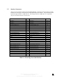
1
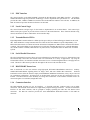
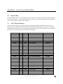
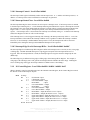
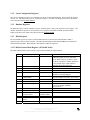
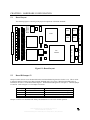
PMC-SIO4AR-SYNC
User’s Manual
QUAD CHANNEL SYNCHRONOUS
SERIAL TO PARALLEL CONTROLLER
WITH DEEP TRANSMIT AND RECEIVE FIFOS
PMC REAR I/O INTERFACE
*** NOT RECOMMENDED FOR NEW DESIGNS ***
*** See PMC66-SIO4BXR-SYNC for New 66MHz PCI Interface***
General Standards Corporation
8302A Whitesburg Drive
Huntsville, AL 35802
Phone: (256) 880-8787
Fax: (256) 880-8788
URL: www.generalstandards.com
E-mail: [email protected]
Revision D
PMC-SIO4AR Documentation History
1.
2.
3.
4.
Rev A - May 2003 – Original rev from PMC-SIO4AR manual.
Rev B – July 2003 – Fixed programmable clock documentation and appendix A table values
Rev C – March 2004 – Fixed errors in bit definitions for some registers/ fixed TOC
Rev D – March 2004 – Product moved to Legacy Status
PREFACE
Copyright © 2012 General Standards Corporation
Additional copies of this manual or other General Standards Corporation literature may be obtained
from:
General Standards Corporation
8302A Whitesburg Drive
Huntsville, Alabama 35802
Telephone: (256) 880-8787
Fax: (256) 880-8788
URL: www.generalstandards.com
The information in this document is subject to change without notice.
General Standards Corporation makes no warranty of any kind with regard to this material, including,
but not limited to, the implied warranties of merchantability and fitness for a particular purpose. Although
extensive editing and reviews are performed before release to ECO control, General Standards
Corporation assumes no responsibility for any errors that may exist in this document. No commitment is
made to update or keep current the information contained in this document.
General Standards Corporation does not assume any liability arising out of the application or use of
any product or circuit described herein, nor is any license conveyed under any patent right of any rights of
others.
General Standards Corporation assumes no responsibility resulting from omissions or errors in this
manual, or from the use of information contained herein.
General Standards Corporation reserves the right to make any changes, without notice, to this product
to improve reliability, performance, function, or design.
All rights reserved
No parts of this document may be copied or reproduced in any form or by any means without prior written
consent of General Standards Corporation.
RELATED PUBLICATIONS
PLX PCI 9080 Data Book
PLX Technology Inc.
390 Potrero Avenue
Sunnyvale, CA 4085
(408) 774-3735
http://www.plxtech.com/
EIA-422-A – Electrical Characteristics of Balanced Voltage Digital Interface Circuits
(EIA order number EIA-RS-422A)
EIA-485 – Standard for Electrical Characteristics of Generators and Receivers for Use in Balanced Digital
Multipoint Systems
(EIA order number EIA-RS-485)
EIA Standards and Publications can be purchased from:
GLOBAL ENGINEERING DOCUMENTS
15 Inverness Way East
Englewood, CO 80112
Phone: (800) 854-7179
http://global.ihs.com/
IEEE P1386 - Standard Mechanic for a Common Mezzanine Card Family: CMC
IEEE P1386.1 - Standard Physical and Environmental Layers for PCI Mezzanine Cards: PMC
Sponsored by the Microprocessor & Microcomputer Standards Committee (MMSC) of the IEEE Computer Society
Copies of IEEE specifications available from:
Institute of Electrical and Electronics Engineers
Service Center
445 Hoes Lane
Piscataway, NJ 08855-1331 USA
http://www.ieee.org/
PCI Local Bus Specification Revision 2.1 June 1, 1995.
Copies of PCI specifications available from:
PCI Special Interest Group
NE 2575 Kathryn Street, #17
Hillsboro, OR 97124
http://www.pcisig.com/
TABLE OF CONTENTS
CHAPTER 1: INTRODUCTION .............................................................................................................................1
1.0
1.1
1.1.1
1.1.2
1.1.3
1.1.4
1.1.5
1.1.6
GENERAL DESCRIPTION..................................................................................................................................1
FUNCTIONAL DESCRIPTION ............................................................................................................................1
PMC INTERFACE ............................................................................................................................................2
LOCAL CONTROL LOGIC.................................................................................................................................2
TRANSMIT/RECEIVE FIFOS ............................................................................................................................2
SERIAL/PARALLEL CONVERTERS....................................................................................................................2
RS422/RS485 TRANSCEIVERS .......................................................................................................................2
CONNECTOR INTERFACE.................................................................................................................................2
CHAPTER 2: LOCAL SPACE REGISTERS .........................................................................................................3
2.0
REGISTER MAP ...............................................................................................................................................3
2.1
GSC FIRMWARE REGISTERS ...........................................................................................................................3
2.1.1 FIRMWARE REVISION: LOCAL OFFSET 0X0000..............................................................................................4
2.1.2 BOARD CONTROL: LOCAL OFFSET 0X0004 ...................................................................................................4
2.1.3 BOARD STATUS: LOCAL OFFSET 0X0008 .......................................................................................................5
2.1.4 CHANNEL TX ALMOST FLAGS: LOCAL OFFSET 0X0010 / 0X0020 / 0X0030 / 0X0040....................................5
2.1.5 CHANNEL RX ALMOST FLAGS: LOCAL OFFSET 0X0014 / 0X0024 / 0X0034 / 0X0044 ....................................5
2.1.6 CHANNEL FIFO: LOCAL OFFSET 0X0018 / 0X0028 / 0X0038 / 0X0048 ..........................................................6
2.1.7 CHANNEL CONTROL/STATUS: LOCAL OFFSET 0X001C / 0X002C / 0X003C / 0X004C ...................................6
2.1.8 INTERRUPT REGISTERS ...................................................................................................................................9
2.1.8.1 INTERRUPT CONTROL: LOCAL OFFSET 0X0060 ...........................................................................................10
2.1.8.2 INTERRUPT STATUS/CLEAR: LOCAL OFFSET 0X0064 ..................................................................................10
2.1.8.3 INTERRUPT EDGE/LEVEL & INTERRUPT HI/LO: LOCAL OFFSET 0X0068 / 0X006C......................................10
2.1.9 IO CONTROL REGISTER: LOCAL OFFSET 0X0090 / 0X0094 / 0X0098 / 0X9C...............................................10
2.1.10 PROGRAMMABLE CLOCK REG: LOCAL OFFSET 0X00A0 / 0X00A4 / 0X00A8 / 0X00AC .............................12
2.1.11 TX COUNT REGISTER: LOCAL OFFSET 0X00B0 / 0X00B4 / 0X00B8 / 0XBC................................................13
2.1.12 RX COUNT REGISTER: LOCAL OFFSET 0X00C0 / 0X00C4 / 0X00C8 / 0XCC................................................13
2.1.13 FEATURES REGISTER: LOCAL OFFSET 0X00FC............................................................................................13
CHAPTER 3: PCI/PMC INTERFACE..................................................................................................................14
3.0
PCI/PMC INTERFACE REGISTERS.................................................................................................................14
3.1
PCI REGISTERS ............................................................................................................................................14
3.1.1 PCI CONFIGURATION REGISTERS .................................................................................................................14
3.1.2 LOCAL CONFIGURATION REGISTERS ............................................................................................................15
3.1.3 RUNTIME REGISTERS ....................................................................................................................................15
3.1.3 DMA REGISTERS .........................................................................................................................................15
3.1.3.1 DMA CHANNEL MODE REGISTER: (PCI 0X80 / 0X94) .................................................................................15
CHAPTER 4: PROGRAMMING...........................................................................................................................16
4.0
4.1
4.2
4.3
4.4
4.5
4.6
4.7
INTRODUCTION .............................................................................................................................................16
RESETS .........................................................................................................................................................16
FIFO ALMOST FLAGS...................................................................................................................................16
DMA............................................................................................................................................................16
INTERRUPTS .................................................................................................................................................17
CLOCK SETUP ...............................................................................................................................................17
PROGRAMMABLE OSCILLATOR / PROGRAMMABLE CLOCKS .........................................................................17
UPPER/LOWER CONNECTOR NAMING CONVENTION ....................................................................................18
CHAPTER 5: HARDWARE CONFIGURATION ...............................................................................................19
5.1
5.2
BOARD LAYOUT ...........................................................................................................................................19
BOARD ID JUMPER J3...................................................................................................................................19
5.3
5.4
INTERFACE CONNECTORS .............................................................................................................................20
TERMINATION RESISTORS ............................................................................................................................21
CHAPTER 6: ORDERING OPTIONS ..................................................................................................................22
6.0
6.0.1
6.0.2
6.0.3
6.1
ORDERING INFORMATION .............................................................................................................................22
FIFO SIZE ....................................................................................................................................................22
INTERFACE CABLE .......................................................................................................................................22
DEVICE DRIVERS ..........................................................................................................................................22
CUSTOM APPLICATIONS ...............................................................................................................................22
APPENDIX A: COMMON PROGRAMMABLE CLOCK REGISTER VALUES...........................................23
APPENDIX B: CALCULATING PROGRAMMABLE CLOCK VALUES ......................................................24
PMC-SIO4AR-SYNC User Manual, Revision: D
General Standards Corporation
8302A Whitesburg Drive Huntsville, AL 35802, Phone: (256) 880-8787
IV
CHAPTER 1: INTRODUCTION
1.0
General Description
The PMC-SI04AR-SYNC board is a four channel serial interface card which provides a simple synchronous serial
interface capability for PCI Mezzanine Card (PMC) applications. The PMC-SIO4AR-SYNC combines a flexible
parallel/serial converter and 8 external FIFOs to provide four fully independent synchronous RS422/RS485 serial
channels. In addition to the standard front edge I/O connector, the PMC-SIO4AR also provides a user interface via
the PMC Rear IO connector. These features, along with a high performance PCI interface engine, give the PMCSIO4AR-SYNC unsurpassed performance in a serial interface card.
The PMC-SIO4AR-SYNC incorporates the following features:
•
•
•
•
•
•
•
•
•
•
•
•
1.1
Four Independent Synchronous Serial Channels
Serial Data Rates up to 10 Mbits/sec
PMC Rear IO User Interface.
SCSI II type 68 pin front edge I/O Connector with optional cable adapter to four DB25 connectors.
Independent Transmit and Receive FIFO Buffers for each Serial Channel – Up to 32k Deep Each
Fast RS485/RS422 Differential Cable Transceivers to Provide Increased Noise Immunity
Programmable Transmit Bit Counts allow for various transmit word lengths
Selectable Transmit Gap Bit Counts allow for a programmed number of clocks between words
Unused Serial Channels can be programmed to provide General Purpose IO capability.
Dual PCI DMA Engine to speed transfers and minimize host I/O overhead
On-Board Programmable Oscillator provides increased flexibility for Baud Rate Clock generation
A variety of device drivers are available, including VxWorks, WinNT, Win2k, Linux, and Labview
Functional Description
Ch1
Ch1 Rx
FIFO
Upper
Ch1 Tx
FIFO
Prog
Osc
PMC
Serial/
Parallel
Ch2 Rx
FIFO
Lower
Ch2
Upper
Ch2 Tx
FIFO
PCI
Bridge
Lower
Control
Logic
Ch3
Ch3 Rx
FIFO
Upper
Ch3 Tx
FIFO
Serial/
Parallel
PMC
Rear
IO
(P4)
Ch4 Rx
FIFO
Lower
Ch4
Upper
Ch4 Tx
FIFO
Lower
Figure 1-1 Block Diagram of PMC-SIO4AR-SYNC
68 Pin
User
(Cable
IF)
1.1.1
PMC Interface
The control interface to the PMC-SIO4AR is through the PCI Mezzanine Card (PMC) interface. An industry
standard PCI9080 bridge chip from PLX Technology is used to implement PCI Specification 2.1. The PCI9080
provides the 32bit, 33MHz (132MBit/sec) interface between the PMC bus and the Local 32 bit bus. In addition, the
PMC P4 connector provides the Rear IO Interface for the board.
1.1.2
Local Control Logic
The control functions and glue logic for the board are implemented in an on-board FPGA. This custom logic
defines local space registers to provide software control over the board functions. These functions include setup,
control, and transfer of data to and from the serial controller chips.
1.1.3
Transmit/Receive FIFOs
Eight independent Transmit and Receive FIFOs provide up to 32kbytes of data buffering per channel for the serial
data. Each channel has a unique transmit and receive FIFO to allow the channels to operate independently. The
FIFOs allow data transfer to continue to/from the IO interface independent of PMC interface transfers and software
overhead. The required FIFO size may depend on several factors including data transfer size, required throughput
rate, and the software overhead (which will also vary based on OS). Deep FIFOs ensure no data is lost for critical
systems.
1.1.4
Serial/Parallel Converters
The serial serial/parallel converters allow various word lengths to be transmitted or received. A Transmit Bit Count
and Transmit Gap Count allow the transmit word to be customized for a variety of applications. By using the
Transmit Bit Counters, the transmit serial data stream can be set to a fixed bit length and allow a fixed gap between
words. The Receive Bit Counter provides the bit length of the last received serial data stream.
1.1.5
RS422/RS485 Transceivers
Data is transferred over the user interface using high-speed, differential RS485/RS422 transceivers. Industry
standard differential RS485 signaling allows for longer, faster, and more reliable data connections. Socketed
termination resistors allow the board to comply with both RS485 and RS422 terminations, or they may be removed
for a multi-drop configuration. All transceivers are bi-directional, so that any pin may be configured to receive or
transmit. This allows the user more flexibility for wiring cable connections. It also enables two SIO4 cards to be
connected together via a standard, straight-thru cable.
1.1.6
Connector Interface
The PMC-SIO4AR provides two user IO interfaces – a front-side card edge connector and a rear IO PMC
connection. The front-side card connector is a high-density 68 pin SCSI II type connector. All four serial channels
interface via this cable connector, and are grouped to simplify separating the cable into four distinct serial
connectors. The Rear IO connector provides the same RS485/RS422 differential interface to the PMC P4
connector.
PMC-SIO4AR-SYNC User Manual, Revision: D
General Standards Corporation
8302A Whitesburg Drive Huntsville, AL 35802, Phone: (256) 880-8787
2
CHAPTER 2: LOCAL SPACE REGISTERS
2.0
Register Map
The PMC-SIO4AR-SYNC is accessed through two sets of registers – PCI Registers (internal to PLX PCI9080) and
GSC Firmware Registers. The GSC Firmware Registers are referred to as Local Space Registers and are described
below. The PCI registers are discussed in Chapter 3.
2.1
GSC Firmware Registers
The GSC Firmware Registers provide the primary control/status for the PMC-SIO4AR board. These registers
define general setup and control functions for the board, including interrupt handling, serial transceiver setup, and
programmable clock functions. The on-board FIFOs which pass data to/from the serial channels are also mapped in
this region. The following table shows the GSC Firmware Registers.
Offset Address
0x0000
0x0004
0x0008
0x000C
0x0010
0x0014
0x0018
0x001C
0x0020
0x0024
0x0028
0x002C
0x0030
0x0034
0x0038
0x003C
0x0040
0x0044
0x0048
0x004C
0x0050-5C
0x0060
0x0064
0x0068
0x006C
0x0070-0x008C
0x0090
0x0094
0x0098
0x009C
Size
D32
D32
D32
--D32
D32
D32
D32
D32
D32
D32
D32
D32
D32
D32
D32
D32
D32
D32
D32
--D32
D32
D32
D32
--D32
D32
D32
D32
Access*
RW
RW
RO
-RW
RW
RW
RW
RW
RW
RW
RW
RW
RW
RW
RW
RW
RW
RW
RW
-RW
RW
RO
RW
-RW
RW
RW
RW
Register Name
Firmware Revision
Board Control
Board Status
RESERVED
Ch 1 Tx Almost Full/Empty
Ch 1 Rx Almost Full/Empty
Ch l 1 Data FIFO
Ch 1 Control/Status
Ch 2 Tx Almost Full/Empty
Ch 2 Rx Almost Full/Empty
Ch 2 FIFO
Ch 2 Control/Status
Ch 3 Tx Almost Full/Empty
Ch 3 Rx Almost Full/Empty
Ch 3 Data FIFO
Ch 3 Control/Status
Ch 4 Tx Almost Full/Empty
Ch 4 Rx Almost Full/Empty
Ch 4 Data FIFO
Ch 4 Control/Status
RESERVED
Interrupt Control
Interrupt Status
Interrupt Edge/Level
Interrupt High/Low
RESERVED
Ch 1 IO Control
Ch 2 IO Control
Ch 3 IO Control
Ch 4 IO Control
Default Value (Hex)
PMC-SIO4AR-SYNC User Manual, Revision: D
General Standards Corporation
8302A Whitesburg Drive Huntsville, AL 35802, Phone: (256) 880-8787
010201XX
00000000
0000000X
-------00070007
00070007
000000XX
0000CC00
00070007
00070007
000000XX
0000CC00
00070007
00070007
000000XX
0000CC00
00070007
00070007
000000XX
0000CC00
00000000
00000000
00000000
FFFF7777
FFFFFFFF
-------00000000
00000000
00000000
00000000
3
0x00A0
0x00A4
0x00A8
0x00AC
0x00B0
0x00B4
0x00B8
0x00BC
0x00C0
0x00C4
0x00C8
0x00CC
0x00D0-0x00F8
0x00FC
D32
D32
D32
D32
D32
D32
D32
D32
D32
D32
D32
D32
--D32
RW
RW
RW
RW
RW
RW
RW
RW
RW
RW
RW
RW
-RO
Ch 1 Prog Clock Divider/Osc
Ch 2 Prog Clock Divider
Ch 3 Prog Clock Divider
Ch4 Prog Clock Divider
Ch 1 Transmit Counters
Ch 2 Transmit Counters
Ch 3 Transmit Counters
Ch 4 Transmit Counters
Ch 1 Receive Counters
Ch 2 Receive Counters
Ch 3 Receive Counters
Ch 4 Receive Counters
RESERVED
Features Register
00129128
00000000
00000000
00000000
00000000
00000000
00000000
00000000
00000000
00000000
00000000
00000000
-------000000XX
* RO = read only, RW = read/write capability
2.1.1
Firmware Revision: Local Offset 0x0000
The Firmware ID register provides version information about the firmware on the board. This is useful for technical
support to identify the firmware version.
D6:0
D7
D15:8
D23:16
D31:24
2.1.2
Firmware Revision
Internal/External FIFOs
Device ID
SIO4 Board ID
Misc
Identifies version of specific firmware
0 = External FIFOs / 1 = Internal FIFOs
02 = SIO4A Standard
02 = PMC-SIO4AR
01 = Features Register at Local Offset 0x00FC.
Board Control: Local Offset 0x0004
The Board Control Register defines the general control functions for the board. The main function in this register
defines the Demand mode DMA channel requests. For Demand mode DMA, there are only two physical DMA
channels which must be shared between the eight serial channels (Rx and TX for each of four channels). The
Demand Mode DMA Channel Request allows the software to multiplex the DMA channels. This is typically
handled by the driver – the end user should have no need to change this register.
D2: 0
D
2
0
1
0
1
0
1
0
1
D3
Demand Mode DMA Channel 0 Request
D
1
0
0
1
1
0
0
1
1
D
0
0
0
0
0
1
1
1
1
Demand Mode DMA 0 Channel
Channel 1 Rx
Channel 1 Tx
Channel 2 Rx
Channel 2 Tx
Channel 3 Rx
Channel 3 Tx
Channel 4 Rx
Channel 4 Tx
Reserved
PMC-SIO4AR-SYNC User Manual, Revision: D
General Standards Corporation
8302A Whitesburg Drive Huntsville, AL 35802, Phone: (256) 880-8787
4
D4:6
Demand Mode DMA Channel 1 Request
D
6
0
1
0
1
0
1
0
1
D31:7
2.1.3
D
5
0
0
1
1
0
0
1
1
D
4
0
0
0
0
1
1
1
1
Demand Mode DMA 1 Channel
Channel 1 Rx
Channel 1 Tx
Channel 2 Rx
Channel 2 Tx
Channel 3 Rx
Channel 3 Tx
Channel 4 Rx
Channel 4 Tx
Reserved
Board Status: Local Offset 0x0008
The Board Status Register gives general overall status for a board. The Board Jumpers are physical jumpers which
can be used to distinguish between boards if multiple SIO4 boards are present in a system.
D0
D1
D31:D2
2.1.4
Board Jumper 0 (0=jumper J3:1-2 installed)
Board Jumper 1 (0=jumper J3:3-4 installed)
Reserved
Channel TX Almost Flags: Local Offset 0x0010 / 0x0020 / 0x0030 / 0x0040
The Tx Almost Flag Registers are used to program the Almost Full and Almost Empty Flags in the transmit FIFOs.
The FIFO almost flags may be used to determine a fill level for a specific transfer size, or used for demand mode
DMA. Setting this register does not automatically program the almost flags – the registers will be programmed
during a FIFO Reset command. See 4.2 FIFO Almost Flags for further information concerning Tx FIFO Almost
Flag programming.
D15:0
D31:16
2.1.5
TX Almost Empty Flag Value
Almost Empty Flag will be asserted when the FIFO contains “Almost Empty Value”
words or fewer.
TX Almost Full Flag Value
Almost Full Flag will be asserted when the FIFO has space for “Almost Full Value”
words or fewer (i.e. FIFO contains (FIFO Size – Almost Full Value) words or more.)
Channel Rx Almost Flags: Local Offset 0x0014 / 0x0024 / 0x0034 / 0x0044
The Rx Almost Flag Registers are used to program the Almost Full and Almost Empty Flags in the receive FIFOs.
The FIFO almost flags may be used to determine a fill level for a specific transfer size, or used for demand mode
DMA. Setting this register does not automatically program the almost flags – the registers will be programmed
during a FIFO Reset command. See 4.2 FIFO Almost Flags for further information concerning Rx FIFO Almost
Flag programming.
D15:0
D31:16
Rx Almost Empty Flag Value
Almost Empty Flag will be asserted when the FIFO contains “Almost Empty Value”
words or fewer.
Rx Almost Full Flag Value
Almost Full Flag will be asserted when the FIFO has space for “Almost Full Value”
words or fewer (i.e. FIFO contains (FIFO Size – Almost Full Value) words or more.)
PMC-SIO4AR-SYNC User Manual, Revision: D
General Standards Corporation
8302A Whitesburg Drive Huntsville, AL 35802, Phone: (256) 880-8787
5
2.1.6
Channel FIFO: Local Offset 0x0018 / 0x0028 / 0x0038 / 0x0048
The Channel FIFO Register passes serial data to/from the serial controller chips. The same register is used to access
both the Transmit FIFO (writes) and Receive FIFO (reads).
D7:0
D31:8
2.1.7
Channel FIFO Data
Reserved
Channel Control/Status: Local Offset 0x001C / 0x002C / 0x003C / 0x004C
The Channel Control/Status Register provides the reset functions and data transceiver enable controls, and the FIFO
Flag status for each channel.
D31:15 / D7:0 Channel Control Bits
D0 Reset Channel TX FIFO (Pulsed)
1 = Reset Channel TX FIFOs.
Notes:
• This value will automatically clear to ‘0’.
• If the Channel TX Almost Flag register is not zero, the Tx Almost Flag Values will
automatically be programmed following the FIFO Reset.
• Software must wait approximately 1ms following a FIFO Reset before accessing the
Local Board Registers again.
D1 Reset Channel Rx FIFO (Pulsed)
1 = Reset Channel Rx FIFOs.
Notes:
• This value will automatically clear to ‘0’.
• If the Channel Rx Almost Flag register is not zero, the Rx Almost Flag Values will
automatically be programmed following the FIFO Reset.
D5:2
Enables for data signals through the transmit and receive buffers to and from the user IO
connector. See 4.8 Upper/Lower Cable Naming Convention for an explanation of
“Upper/Lower”.
Note: If D5:D2 = “0000”, the channel is set to General Purpose IO. This means External Sync
Logic is disabled and the IO signals are controlled from the Channel IO Control Register.
D2 Channel Lower Transmit Data Enable
1 = Channel Lower TxD driven to IO connector.
0 = Channel Lower TxD disabled (tristate).
D3 Channel Upper Transmit Data Enable
1 = Channel Upper TxD driven to IO connector.
0 = Channel Upper TxD disabled (tristate).
D4 Channel Lower Receive Data Enable
1 = Channel Lower RxD received in from IO connector.
0 = Channel Lower RxD disabled (tristate).
D5 Channel Upper Rx Data Enable
1 = Channel Upper RxD received in from IO connector.
Note: Upper RxD will NOT be enabled if D4 (Lower RxD) also enabled.
0 = Channel Upper RxD disabled (tristate).
PMC-SIO4AR-SYNC User Manual, Revision: D
General Standards Corporation
8302A Whitesburg Drive Huntsville, AL 35802, Phone: (256) 880-8787
6
D7:6
Reserved
PMC-SIO4AR-SYNC User Manual, Revision: D
General Standards Corporation
8302A Whitesburg Drive Huntsville, AL 35802, Phone: (256) 880-8787
7
D16
D17
D18
D19
D20
D21
D22
D23
D24
D25
D26
D27
D28
D29
D30
Receive Enable
0 = Receiver Disabled
1 = Receiver Enabled
Transmit Enable
0 = Transmitter Disabled
1 = Transmitter Enabled
Stop Transmit On FIFO Empty
0 = Transmitter remains enabled under software control (D17)
1 = Transmitter will be disabled (D17=0) when transmitter becomes empty
RxClk Polarity
1 = Clock on Rising Edge (default)
0 = Clock on Falling Edge
TxClk Polarity
1 = TxClk on Rising Edge (default)
0 = TxClk on Falling Edge
Idle TxClk
1 = TxClk present while Idle (not Transmitting)
0 = No TxClk while Idle (TxClk present only when Envelope present)
TxClk Source
0 = TxClk Source Internal
1 = TxClk Source External
Receive Bit Count Reset
1 = Reset Rx Bit Count
Receive MSB/LSB
0 = Receive MSB first
1 = Receive LSB first
Transmit MSB/LSB
0 = Transmit MSB first
1 = Transmit LSB first
Receive Envelope Polarity
1 = Rx Envelope Active Lo
0 = Rx Envelope Active Hi
Transmit Envelope Polarity
1 = Tx Envelope Active Lo
0 = Tx Envelope Active Hi
Internal Loopback
0 = Normal Mode
1 = Internal Loopback (for High speed test)
Dual Sync
0 = Normal Mode
1 = Dual Sync Mode
Reserved
D31 / D15:8
D8
D9
D10
D11
D12
D13
D14
D15
D31
Channel Status Bits
Channel Tx FIFO Empty Flag Lo
Channel Tx FIFO Almost Empty Flag Lo
Channel Tx FIFO Almost Full Flag Lo
Channel Tx FIFO Full Flag Lo
Channel Rx FIFO Empty Flag Lo
Channel Rx FIFO Almost Empty Flag Lo
Channel Rx FIFO Almost Full Flag Lo
Channel Rx FIFO Full Flag Lo
Receive Count Error
(Active Low -- 0=Tx Empty)
(Active Low -- 0=Tx Almost Empty)
(Active Low -- 0=Tx Almost Full)
(Active Low -- 0=Tx Full)
(Active Low -- 0=Rx Empty)
(Active Low -- 0=Rx Almost Empty)
(Active Low -- 0=Rx Almost Full)
(Active Low -- 0=Rx Full)
PMC-SIO4AR-SYNC User Manual, Revision: D
General Standards Corporation
8302A Whitesburg Drive Huntsville, AL 35802, Phone: (256) 880-8787
8
2.1.8
Interrupt Registers
There are 32 on-board interrupt sources (in addition to USC interrupts and PLX interrupts), each of which may be
individually enabled. Four interrupt registers control the on-board interrupts – Interrupt Control, Interrupt Status,
Interrupt Edge/Level, and Interrupt Hi/Lo. The 32 Interrupt sources are:
IRQ #
IRQ0
IRQ1
IRQ2
IRQ4:3
IRQ5
IRQ6
IRQ8:7
IRQ9
IRQ10
IRQ12:11
IRQ13
IRQ14
IRQ15
IRQ16
IRQ17
IRQ18
IRQ19
IRQ20
IRQ21
IRQ22
IRQ23
IRQ24
IRQ25
IRQ26
IRQ27
IRQ28
IRQ29
IRQ30
IRQ31
Source
Unused
Channel 1 Tx FIFO Almost Empty
Channel 1 Rx FIFO Almost Full
Unused
Channel 2 Tx FIFO Almost Empty
Channel 2 Rx FIFO Almost Full
Unused
Channel 3 Tx FIFO Almost Empty
Channel 3 Rx FIFO Almost Full
Unused
Channel 4 Tx FIFO Almost Empty
Channel 4 Rx FIFO Almost Full
Unused
Channel 1 Tx FIFO Empty
Channel 1 Tx FIFO Full
Channel 1 Rx FIFO Empty
Channel 1 Rx FIFO Full
Channel 2 Tx FIFO Empty
Channel 2 Tx FIFO Full
Channel 2 Rx FIFO Empty
Channel 2 Rx FIFO Full
Channel 3 Tx FIFO Empty
Channel 3 Tx FIFO Full
Channel 3 Rx FIFO Empty
Channel 3 Rx FIFO Full
Channel 4 Tx FIFO Empty
Channel 4 Tx FIFO Full
Channel 4 Rx FIFO Empty
Channel 4 Rx FIFO Full
Default Level
-Rising Edge
Rising Edge
-Rising Edge
Rising Edge
-Rising Edge
Rising Edge
-Rising Edge
Rising Edge
-Rising Edge
Rising Edge
Rising Edge
Rising Edge
Rising Edge
Rising Edge
Rising Edge
Rising Edge
Rising Edge
Rising Edge
Rising Edge
Rising Edge
Rising Edge
Rising Edge
Rising Edge
Rising Edge
Alternate Level
-Falling Edge
Falling Edge
-Falling Edge
Falling Edge
-Falling Edge
Falling Edge
-Falling Edge
Falling Edge
-Falling Edge
Falling Edge
Falling Edge
Falling Edge
Falling Edge
Falling Edge
Falling Edge
Falling Edge
Falling Edge
Falling Edge
Falling Edge
Falling Edge
Falling Edge
Falling Edge
Falling Edge
Falling Edge
For all interrupt registers, the IRQ source (IRQ31:IRQ0) will correspond to the respective data bit (D31:D0) of each
register. (D0 = IRQ0, D1 = IRQ1, etc.)
All FIFO interrupts are edge triggered active high. This means that an interrupt will be asserted (assuming it is
enabled) when a FIFO Flag transitions from FALSE to TRUE (rising edge triggered) or TRUE to FALSE (falling
edge). For example: If Tx FIFO Empty Interrupt is set for Rising Edge Triggered, the interrupt will occur when the
FIFO transitions from NOT EMPTY to EMPTY. Likewise, if Tx FIFO Empty Interrupt is set as Falling Edge
Triggered, the interrupt will occur when the FIFO transitions from EMPTY to NOT EMPTY.
All Interrupt Sources share a single interrupt request back to the PCI9080 PLX chip. Likewise, all USC interrupt
sources share a single interrupt request back to the interrupt controller and must be further qualified in the USC
chip. See Section 4.4 Interrupts for further interrupt programming information.
PMC-SIO4AR-SYNC User Manual, Revision: D
General Standards Corporation
8302A Whitesburg Drive Huntsville, AL 35802, Phone: (256) 880-8787
9
2.1.8.1 Interrupt Control: Local Offset 0x0060
The Interrupt Control register individually enables each interrupt source. A ‘1’ enables each interrupt source; a ‘0’
disables. An interrupt source must be enabled for an interrupt to be generated.
2.1.8.2 Interrupt Status/Clear: Local Offset 0x0064
The Interrupt Status Register shows the status of each respective interrupt source. If an interrupt source is enabled
in the Interrupt Control Register, a ‘1’ in the Interrupt Status Register indicates the respective interrupt has occurred.
The interrupt source will remain latched until the interrupt is cleared, either by writing to the Interrupt Status/Clear
Register with a ‘1’ in the respective interrupt bit position, or the interrupt is disabled in the Interrupt Control
register. If an interrupt source is not asserted or the interrupt is not enabled, writing a ‘1’ to that bit in the Interrupt
Status/Clear Register will have no effect on the interrupt.
If the interrupt source is a level triggered interrupt (USC interrupt), the interrupt status may still be ‘1’ even if the
interrupt is disabled. This indicates the interrupt condition is true, regardless of whether the interrupt is enabled.
Likewise, if a level interrupt is enabled and the interrupt source is true, the interrupt status will be reasserted
immediately after clearing the interrupt, and an additional interrupt will be requested.
2.1.8.3 Interrupt Edge/Level & Interrupt Hi/Lo: Local Offset 0x0068 / 0x006C
The Interrupt Edge/Level and Interrupt Hi/Lo Registers define each interrupt source as level hi, level lo, rising edge,
or falling edge. All PMC-SIO4AR interrupts are edge triggered except the USC interrupts which are level
triggered. Since the interrupt behavior is fixed, the Interrupt Edge/Level register cannot be changed by the user.
(Read Only)
The FIFO Flags may be defined as rising edge or falling edge via the Interrupt Hi/Lo Register. For example, a
rising edge of the TX Empty source will generate an interrupt when the TX FIFO becomes empty. Defining the
source as falling edge will trigger an interrupt when the TX FIFO becomes “NOT Empty”.
2.1.9
IO Control Register: Local Offset 0x0090 / 0x0094 / 0x0098 / 0x9C
When a channel is setup for General Purpose IO in the Channel Control Register, the IO Control Register controls
the function of the General Purpose IO pins.
D7:0
IO Setup
D0
0 =>
1 =>
D1
0 =>
CTS/GPIO0 = Input
CTS/GPIO0 = Output
Lower RxD/GPIO1 = Input
DCD/GPIO3
= Input
1 =>
Lower RxD/GPIO1 = Output
DCD/GPIO3
= Output
D2
0 =>
Lower RxClk/GPIO2 = Input
1 =>
Lower RxClk/GPIO2 = Output
D3
0 =>
DCD/GPIO3 = Input (D1 must be set to 0 - Input)
1 =>
DCD/GPIO3 = Output (D1 must be set to 1 - Output)
D4
0 =>
Upper RxD /GPIO4 = Input (D1 must be set to 1 - Output)
1 =>
Upper RxD /GPIO4 = Output (D1 must be set to 0 - Input)
D5
0 =>
Upper RxClk /GPIO5 = Input (D2 must be set to 1 - Output)
1 =>
Upper RxClk /GPIO5 = Output (D2 must be set to 0 - Input)
D7:D6 Reserved
PMC-SIO4AR-SYNC User Manual, Revision: D
General Standards Corporation
8302A Whitesburg Drive Huntsville, AL 35802, Phone: (256) 880-8787
10
D15:8
Output Value / Input Latch
If a pin is setup as an Output (via IO Setup D7-D0), D15-D8 define the output value.
D8
D9
D10
D11
D12
D13
D15:D14
CTS/GPIO0 Output Value
Lower RxD/GPIO1 Output Value
Lower RxClk/GPIO2 Output Value
DCD/GPIO3 Output Value
Upper RxD /GPIO4 Output Value
Upper RxClk /GPIO5 Output Value
Reserved
If a pin is setup as an Input (via IO Setup D7-D0), D15-D8 define whether the Input Value is
latched (1). If the input is latched, the input latch behavior is defined by bits D31-D24. Once
an input is latched, resetting the corresponding bit below will clear the latched input.
D8
D9
D10
D11
D12
D13
D15:D14
CTS/GPIO0 Input latched
Lower RxD/GPIO1 Input latched
Lower RxClk/GPIO2 Input latched
DCD/GPIO3 Input latched
Upper RxD /GPIO4 Input latched
Upper RxClk /GPIO5 Input latched
Reserved
D23:16 Input Value
If a pin is setup as an Input (via IO Setup D7-D0), D23-D16 reflect the input value. If an
input is defined as latched, a ‘1’ will indicate the latched condition occurred.
D16
D17
D18
D19
D20
D21
D23:D22
CTS/GPIO0 Input Value
Lower RxD/GPIO1 Input Value
Lower RxClk/GPIO2 Input Value
DCD/GPIO3 Input Value
Upper RxD /GPIO4 Input Value
Upper RxClk /GPIO5 Input Value
Reserved
D31:24 Input Latch
If a pin is setup as an Input (via IO Setup D7-D0), and D15-D8 define an input as latched,
then D31-D24 define the latching condition – lo level, hi level, falling edge, or rising edge.
D30
Level (0) / Edge (1) latched inputs
D24
CTS/GPIO0 Polarity
0 =>
If D30=0, level lo
If D30=1, level hi
1 =>
If D30=0, falling edge
If D30=1, rising edge
Lower RxD/GPIO1 Polarity
0 =>
If D30=0, level lo
If D30=1, level hi
1 =>
If D30=0, falling edge
If D30=1, rising edge
D25
PMC-SIO4AR-SYNC User Manual, Revision: D
General Standards Corporation
8302A Whitesburg Drive Huntsville, AL 35802, Phone: (256) 880-8787
11
D26
Lower RxClk/GPIO2 Polarity
0 =>
If D30=0, level lo
If D30=1, level hi
1 =>
If D30=0, falling edge
If D30=1, rising edge
DCD/GPIO3 Polarity
0 =>
If D30=0, level lo
If D30=1, level hi
1 =>
If D30=0, falling edge
If D30=1, rising edge
Upper RxD /GPIO4 Polarity
0 =>
If D30=0, level lo
If D30=1, level hi
1 =>
If D30=0, falling edge
If D30=1, rising edge
Upper RxClk /GPIO5 Polarity
0 =>
If D30=0, level lo
If D30=1, level hi
1 =>
If D30=0, falling edge
If D30=1, rising edge
D27
D28
D29
D31
Reserved
2.1.10 Programmable Clock Reg: Local Offset 0x00A0 / 0x00A4 / 0x00A8 / 0x00AC
The Programmable Clock Registers allow the user to program the on-board programmable oscillator and configure
the channel clock post-dividers. Since there is only a single programmable oscillator, the output of this oscillator
will be used as the input to all four channel clock post-divers. Figure 2-1 shows the Programmable clock registers.
FPGA
Offset 0x00A0
Ch1 Prog Clk Reg
Prog Osc Control
On-Board
Programmable
Oscillator
Prog Oscillator Value
D23:D0
Ch1 Post-Divider
D31:D24
Ch1 Prog Clk
Prog Osc Clk
Offset 0x00A4
Ch2 Prog Clk Reg
D23:D0 = 0x000000
Ch2 Post-Divider
D31:D24
Ch2 Prog Clk
Offset 0x00A8
Ch3 Prog Clk Reg
D23:D0 = 0x000000
Ch3 Post-Divider
D31:D24
Ch3 Prog Clk
Offset 0x00AC
Ch4 Prog Clk Reg
D23:D0 = 0x000000
Ch4 Post-Divider
D31:D24
Ch4 Prog Clk
Figure 2-1: Channel Programmable Clock Registers
PMC-SIO4AR-SYNC User Manual, Revision: D
General Standards Corporation
8302A Whitesburg Drive Huntsville, AL 35802, Phone: (256) 880-8787
12
Loading the Programmable Clock Register for Channel 1 (Offset 0x00A0) will automatically program the on-board
oscillator. See Section 4.6 Programmable Oscillator for more information of programming the on-board oscillator.
Since the On-Board Programmable Oscillator has a minimum clock frequency of 400 kHz, bits D31:D24 of the
Programmable Clock Register may be used to further “Post Divide” the Programmable Oscillator input. This allows
for programmable clock frequencies below 2 kHz to be obtained.
For Channel 1 (Offset 0x00A0):
D22:0
D23
Programmable Oscillator Program Value
Programming In Progress Status
After writing the Ch1 Programmable Clock Register, this bit will remain ‘1’ while the on-board
oscillator is being programmed.
D31:24 Ch1 Programmable Clock Post-Divide Value (0-255)
NOTE: If the post divide value is set to 0x00 or 0x01, no post divide will be performed.
(Programmable Clock Frequency = Programmable Oscillator Frequency)
For Channels 2-4 (Offsets 0x00A4 / 0x00A8 / 0x00AC):
D23:0 0x000000
D31:24 Programmable Clock Post-Divide Value (0-255)
NOTE: If the post divide value is set to 0x00 or 0x01, no post divide will be performed.
(Programmable Clock Frequency = Programmable Oscillator Frequency)
2.1.11 Tx Count Register: Local Offset 0x00B0 / 0x00B4 / 0x00B8 / 0xBC
D15..0 Transmit Bit Count
These bits indicate the number of consecutive bits the SIO4 should send in each transmit word.
This value is also used to flag an error if the specified count is not received during a receive cycle.
D31..16 Gap Bit Count
If transmit enable is set, these bits indicate the delay, in transmit clock cycles, between transmitted
words. To output a continuous stream of bits, this value may be set to zero. These bits have no
affect if the SIO4 is in receive mode.
2.1.12 Rx Count Register: Local Offset 0x00C0 / 0x00C4 / 0x00C8 / 0xCC
D15..0 Receive Bit Count
If receive enable is set, these bits indicate the size, in bits, of the last received word. These bits
have no affect if the SIO4 is in transmit mode.
2.1.13 Features Register: Local Offset 0x00FC
The Features Register allows software to account for added features in the firmware versions. Bits will be assigned
as new features are added.
D3:0
D4
D31:5
Programmable Clock Configuration
FIFO Counters/Size Present
RESERVED
–
01 = ICD2053B
PMC-SIO4AR-SYNC User Manual, Revision: D
General Standards Corporation
8302A Whitesburg Drive Huntsville, AL 35802, Phone: (256) 880-8787
13
CHAPTER 3: PCI/PMC INTERFACE
3.0
PCI/PMC Interface Registers
A PCI9080 I/O Accelerator from PLX Technology handles the PCI/PMC Interface. The PCI/PMC interface is
compliant with the 5V, 33MHz 32-bit PCI Specification 2.1. The PCI9080 provides dual DMA controllers for fast
data transfers to and from the on-board FIFOs. Fast DMA burst accesses provide for a maximum burst throughput
of 132MB/s to the PCI interface. To reduce CPU overhead during DMA transfers, the controller also implements
Chained (Scatter/Gather) DMA, as well as Demand Mode DMA.
Since many features of the PCI9080 are not utilized in this design, it is beyond the scope of this document to
duplicate the PCI9080 User’s Manual. Only those features, which will clarify areas specific to the PMC-SIO4AR
are detailed here. Please refer to the PCI9080 User’s Manual (See Related Publications) for more detailed
information. Note that the BIOS configuration and software driver will handle most of the PCI9080 interface.
Unless the user is writing a device driver, the details of this PCI/PMC Interface Chapter may be skipped.
3.1
PCI Registers
The PLX 9080 contains many registers, many of which have no effect on the PMC-SIO4AR performance. The
following section attempts to filter the information from the PCI9080 manual to provide the necessary information
for a PMC-SIO4AR specific driver.
The PMC-SIO4AR uses an on-board serial EEPROM to initialize many of the PCI9080 registers after a PCI Reset.
This allows board specific information to be preconfigured.
3.1.1
PCI Configuration Registers
The PCI Configuration Registers allow the PCI controller to identify and control the cards in a system.
PCI device identification is provided by the Vendor ID/Device ID (Addr 0x0000) and Sub-Vendor ID/Sub-Device
ID Registers (0x002C). The following definitions are unique to the General Standards SIO4A boards. All drivers
should verify the ID/Sub-ID information before attaching to this card. These values are fixed via the Serial
EEPROM load following a PCI Reset, and cannot be changed by software.
Vendor ID
Device ID
Sub-Vendor ID
Sub-Device ID
0x10B5
0x9080
0x10B5
0x2401
PLX Technology
PCI9080
PLX Technology
GSC SIO4
The configuration registers also setup the PCI IO and Memory mapping for the PMC-SIO4AR. The PCI9080 is
setup to use PCIBAR0 and PCIBAR1 to map the internal PLX registers into PCI Memory and IO space
respectively. PCIBAR2 will map the Local Space Registers into PCI memory space, and PCIBAR3 is unused.
Typically, the OS will configure the PCI configuration space.
For further information of the PCI configuration registers, please consult the PLX Technology PCI9080 Manual.
PMC-SIO4AR-SYNC User Manual, Revision: D
General Standards Corporation
8302A Whitesburg Drive Huntsville, AL 35802, Phone: (256) 880-8787
14
3.1.2
Local Configuration Registers
The Local Configuration registers give information on the Local side implementation. These include the required
memory size. The SIO4 memory size is initialized to 4k Bytes. All other Local Registers initialize to the default
values described in the PCI9080 Manual.
3.1.3
Runtime Registers
The Runtime registers consist of mailbox registers, doorbell registers, and a general-purpose control register. The
mailbox and doorbell registers are not used and serve no purpose on the PMC-SIO4AR. All other Runtime
Registers initialize to the default values described in the PCI9080 Manual.
3.1.3
DMA Registers
The Local DMA registers are used to setup the DMA transfers to and from the on-board FIFOs. DMA is
supported only to the four FIFO locations. The PMC-SIO4AR supports both Demand (DREQ# controlled) and
Non-Demand mode DMA. Both Channel 0 and Channel 1 DMA are supported.
3.1.3.1 DMA Channel Mode Register: (PCI 0x80 / 0x94)
The DMA Channel Mode register must be setup to match the hardware implementation
Bit
D1:0
Description
Local Bus Width
Value
11 = 32 bit
D5:2
D6
D7
D8
Internal Wait States
Ready Input Enable
Bterm# Input Enabled
Local Burst Enable
0000 = Unused
1 = Enabled
0 = Unused
1 = Supported
D9
D10
D11
D12
D13
D14
D15
D16
D17
D31:18
Chaining Enable (Scatter
Gather DMA)
Done Interrupt Enable
Local Addressing Mode
Demand Mode Enable
Write & Invalidate Mode
DMA EOT Enable
DMA Stop Data
Transfer Enable
DMA Clear Count Mode
DMA Channel Interrupt
Select
Reserved
X
X
1 = No Increment
X
Notes
Although the serial FIFOs only contain 8 bits
of data, the register access is still a 32bit
access. While it may be possible to “pack”
the data by setting the Local Bus Width to 8,
it is beyond the scope of this manual to
determine if/how this could work.
Bursting allows fast back-to-back accesses to
the FIFOs to speed throughput
DMA source addr, destination addr, and byte
count are loaded from memory in PCI Space.
DMA Done Interrupt
DMA to/from FIFOs only
Demand Mode DMA is supported for FIFO
accesses on the PMC-SIO4AR.
(See Section 4.3)
X
0 = Unused
0 = BLAST
terminates DMA
0 = Unused
X
0
PMC-SIO4AR-SYNC User Manual, Revision: D
General Standards Corporation
8302A Whitesburg Drive Huntsville, AL 35802, Phone: (256) 880-8787
15
CHAPTER 4: PROGRAMMING
4.0
Introduction
This section addresses common programming questions when developing an application for the SIO4.
4.1
Resets
Each serial channel provides control for two unique reset sources: a Transmit FIFO Reset, and a Receive FIFO
Reset. All resets are controlled from the GSC Channel Control/Status Registers.
The FIFO resets allow each individual FIFO (Tx and Rx) to be reset independently. In addition to clearing the
FIFO, the Almost Empty and Almost Full flags are programmed following a FIFO reset. If the FIFO Almost Values
are set to zero prior to a FIFO reset, the Almost Empty/Full flags are NOT programmed (the FIFO Flags will be set
at their default value of 7). Section 4.2 provides further information about the FIFO Almost Flags.
4.2
FIFO Almost Flags
The FIFO Almost Empty and Almost Full flags on the PMC-SIO4AR provide a way for the user to approximate the
amount of data in the FIFO. This is useful in determining when a data transfer is complete or determining the
amount of data which can be safely read from/written to the FIFO. The flags are also used during Demand Mode
DMA to set the request levels. The Almost Flags are fully programmable by the user.
Each channel provides two 32 bit registers for setting the Almost Full/Empty values: the TX FIFO Almost Register
(See Section 2.1.5) and the RX FIFO Almost Register (See Section 2.1.6). Each of these registers is further divided
into two 16 bit words: D31-D16 = Almost Full Value; D15-D0 = Almost Empty Value.
The Almost Flag value represents the number of bytes from each respective “end” of the FIFO. The Almost Empty
value represents the number of bytes from empty, and the Almost Full value represents the number of bytes from
full (NOT the number of bytes from empty). For example, the default value of “0x0007 0007” in the FIFO Almost
Register means that the Almost Empty Flag will indicate when the FIFO holds 0x0007 bytes or fewer, and will
transition as the 8th byte is read or written. The Almost Full Flag indicates the FIFO contains (FIFO Size – 0x7)
bytes or more. For the standard 32Kbyte FIFO, an Almost Full value of 0x7 will cause the Almost Full flag to be
asserted when the FIFO contains 32761 (32k – 7) or more bytes of data .
The values placed in the FIFO Almost Registers are programmed to the FIFO chips whenever a FIFO reset is
performed. The proper steps to program these values are:
•
•
•
Set the respective FIFO Almost Register(s)
Perform a FIFO reset of the respective FIFO
The value in the almost register is now programmed into the FIFO chips
If either (or both) FIFO Almost Empty Register or FIFO Almost Full Register is set to a value of 0x0000 during a
FIFO reset, the Almost Flags will not be programmed and the flags will be set to the FIFO chip default of 7 bytes
from empty and 7 bytes from full.
4.3
DMA
The PCI DMA functionality allows data to be transferred between host memory and the PMC-SIO4AR onboard
FIFOs with the least amount of CPU overhead. The PCI9080 bridge chip handles all PCI DMA functions, and the
device driver should handle the details of the DMA transfer.
PMC-SIO4AR-SYNC User Manual, Revision: D
General Standards Corporation
8302A Whitesburg Drive Huntsville, AL 35802, Phone: (256) 880-8787
16
There are two DMA modes – Demand Mode DMA and Non-Demand Mode DMA. Demand Mode DMA refers to
data being transferred on demand. For receive, this means data will be transferred as soon as it is received into the
FIFO. Likewise, for transmit, data will be transferred to the FIFOs as long as the FIFO is not Almost Full. The
disadvantage to Demand Mode DMA is that the DMA transfers are dependent on the user data interface. If the user
data interface hangs, the Demand mode DMA transfer will also stop. If a timeout occurs, there is no way to
determine the exact amount of data transferred before it was aborted.
On the other hand, Non-Demand Mode DMA does not check the FIFO empty/full flags before or during the data
transfer – it simply assumes there is enough available FIFO space to complete the transfer. If the transfer size is
larger than the available data, the transfer will complete with invalid results.
Non-Demand Mode DMA is the safer mode, but it may require more user intervention to ensure the requested data
size is available. Demand Mode DMA requires less software control, but runs the risk of losing data due to an
incomplete transfer. The user will need to evaluate each situation separately to decide whether DMA is necessary,
and if so, which mode.
4.4
Interrupts
The PMC-SIO4AR has a number of interrupt sources which are passed to the host CPU via the PCI Interrupt A.
Since there is only one physical interrupt source, the interrupts pass through a number of “levels” to get multiplexed
onto this single interrupt. The interrupt originates in the PCI9080 PCI Bridge, which combines the internal PLX
interrupt sources (DMA) with the local space interrupt. The driver will typically take care of setting up and
handling the PCI9080 interrupts. The single Local Interrupt is made up of the interrupt sources described in Section
2.1.10. . The user should be aware that interrupts must be enabled at each level for an interrupt to occur. For
example, if a FIFO interrupt is used, it must be setup and enabled in the GSC Firmware Interrupt Control Register,
as well as enabled in the PCI9080. In addition, the interrupt must be acknowledged and/or cleared at each level
following the interrupt.
4.5
Clock Setup
Figure 4-1 shows the relationship of the various clock sources on the PMC-SIO4AR board. These clock sources
can be most simply viewed in three sections: On-Board Programmable Clocks, IO connector Clocks, and USC
Clocks.
The Programmable Clocks consist of a single on-board programmable oscillator and four post-divide clocks (one
for each channel). The single programmable oscillator clock is used as the input for each of the programmable
clock post dividers, which will allow each channel to have a unique programmable clock input. These
programmable clocks are further described in sections 2.1.12 and 4.6.
The IO Connector Clocks consist of the cable RxClk and cable TxClk for each channel. The RxClk is always an
input and the cable TxClk is always an output.
4.6
Programmable Oscillator / Programmable Clocks
The On-Board Programmable Oscillator is programmed by writing to the Channel 1 Programmable Clock Register
at Local Address offset 0x00A0 (See Section 2.1.12). In order to program the oscillator, it is necessary to calculate
a “control word” to program the correct oscillator frequency. Cypress Semiconductor provides a Windows program
called BitCalc to assist in calculating this value. This program should be included with the documentation package.
If not, it is available from General Standards (contact tech support). The clock generator device is an ICD2053B
with an input frequency of 20MHz. The default oscillator value at power up or following a board reset is 20MHz.
The actual transmit clock/data speed will be one half the frequency of the programmable oscillator, or 10 MHz after
power up.
PMC-SIO4AR-SYNC User Manual, Revision: D
General Standards Corporation
8302A Whitesburg Drive Huntsville, AL 35802, Phone: (256) 880-8787
17
The output frequency of the programmable oscillator may be programmed from 20MHz to a minimum of about 400
kHz. Since a slower oscillator than 400 KHz may be required, bits D31:D24 of the Programmable Clock Registers
allow the user to further divide the input clock. There is a separate post-divider for each serial channel, so each
channel can have a unique clock frequency.
For further information, Section 2.1.12 details the Programmable Clock registers. Section 4.5 Clock Setup
provides information on how the programmable clocks can be best utilized. Appendix A provides common
frequencies and their associated programmable oscillator values. Appendix B describes how to calculate
programmable clock register values for frequencies other than those listed in Appendix A.
NOTE: Bit D23 of the Ch 1 Prog Clock Divider is used to indicate when the clock chip is in the process of
programming. After setting a value in this register, software should wait until bit D23 clears before proceeding on
with program. Otherwise indeterminate operation of the clock may occur.
4.7
Upper/Lower Connector Naming Convention
Since all the cable transceivers are bidirectional, the serial Data and Clock signals can be transmitted or received on
two separate IO connector pins. The naming convention “Upper” and “Lower” is used in order to differentiate
between these two pins with identical function. Typically, one pin is used for receive data, and the other pin is used
for transmit. Separate controls for the transmit / receive enables allow the user flexibility to monitor the transmit
line or perform a standalone loop back test. This also allows two SIO4 boards to be connected directly or two
channels to be connected directly using standard cabling options by simply configuring the transmit and receive pins
correctly.
PMC-SIO4AR-SYNC User Manual, Revision: D
General Standards Corporation
8302A Whitesburg Drive Huntsville, AL 35802, Phone: (256) 880-8787
18
CHAPTER 5: HARDWARE CONFIGURATION
5.1
Board Layout
The following figure is a drawing of the physical components of the PMC-SIO4AR:
R
P
1
R
P
4
FIFO
C
o
n
n
FIFO
P
4
FPGA
68
P
i
n
FIFO
R
P
2
R
P
3
P
M
C
FIFO
R
I
O
R
P
5
PLX
PCI9080
R
P
6
1
3
5
7
J3
2
4
6
8
P
M
C
P
M
C
P
1
P
2
Figure 5-1: Board Layout
5.2
Board ID Jumper J3
Jumper J3 allows the user to set the Board ID in the GSC Board Status Register (See Section 2.1.3). This is useful
to uniquely identify a board if more than one PMC-SIO4AR card is in a system. When the Board ID jumper is
installed, it will read ‘0’ in the Board Status Register. The Board Status Register bit will report ‘1’ when the jumper
is removed. Refer to Figure 5.1-1 for Jumper J3 location.
J3 Jumper
1-2
3-4
5-6
7-8
Description
Board ID 0
Board ID 1
Reload FPGA on PCI Reset
PLX EEPROM Config
Notes
Defines Board ID 0 In Board Status Register
Defines Board ID 1 In Board Status Register
Should be installed for normal operation
Must be installed for normal operation
Jumpers 5/6 and 7/8 are installed at the factory and should not be removed for normal operation.
PMC-SIO4AR-SYNC User Manual, Revision: D
General Standards Corporation
8302A Whitesburg Drive Huntsville, AL 35802, Phone: (256) 880-8787
19
5.3
Interface Connectors
There are two user interface connections on the PMC-SIO4AR - A SCSI II type 68-pin connector (female)
mounted to the front edge of the board (P2), and the PMC P4 Rear IO Connector. The part number for the
68 pin front edge connector is AMP 787170-7. The mating connector is AMP 749111-6 or equivalent.
The pin out for both connectors is shown below.
P2, Row A
No Connect
No Connect
No Connect
No Connect
Ch1 Upper Envelope / IO 0 +
Ch1 Upper Envelope / IO 0 Ch1 Lower RxD/TxD / IO 1+
Ch1 Lower RxD/TxD / IO 1 Ch1 Lower RxClk/TxClk / IO 2 +
Ch1 Lower RxClk/TxClk / IO 2 Ch1 Lower Envelope / IO 3 +
Ch1 Lower Envelope / IO 3 Ch1 Upper RxD/TxD / IO 4 +
Ch1 Upper RxD/TxD / IO 4 Ch1 Upper RxClk/TxClk/ IO 5+
Ch1 Upper RxClk/TxClk / IO 5 Ground
Ground
Ch2 Upper Envelope / IO 0 +
Ch2 Upper Envelope / IO 0 Ch2 Lower RxD/TxD / IO 1+
Ch2 Lower RxD/TxD / IO 1 Ch2 Lower RxClk/TxClk / IO 2 +
Ch2 Lower RxClk/TxClk / IO 2 Ch2 Lower Envelope / IO 3 +
Ch2 Lower Envelope / IO 3 Ch2 Upper RxD/TxD / IO 4 +
Ch2 Upper RxD/TxD / IO 4 Ch2 Upper RxClk/TxClk/ IO 5+
Ch2 Upper RxClk/TxClk / IO 5 No Connect
No Connect
No Connect
No Connect
Pin #
1
2
3
4
5
6
7
8
9
10
11
12
13
14
15
16
17
18
19
20
21
22
23
24
25
26
27
28
29
30
31
32
33
34
P2, Row B
No Connect
No Connect
No Connect
No Connect
Ch3 Upper Envelope / IO 0 +
Ch3 Upper Envelope / IO 0 Ch3 Lower RxD/TxD / IO 1+
Ch3 Lower RxD/TxD / IO 1 Ch3 Lower RxClk/TxClk / IO 2 +
Ch3 Lower RxClk/TxClk / IO 2 Ch3 Lower Envelope / IO 3 +
Ch3 Lower Envelope / IO 3 Ch3 Upper RxD/TxD / IO 4 +
Ch3 Upper RxD/TxD / IO 4 Ch3 Upper RxClk/TxClk/ IO 5+
Ch3 Upper RxClk/TxClk / IO 5 Ground
Ground
Ch4 Upper Envelope / IO 0 +
Ch4 Upper Envelope / IO 0 Ch4 Lower RxD/TxD / IO 1+
Ch4 Lower RxD/TxD / IO 1 Ch4 Lower RxClk/TxClk / IO 2 +
Ch4 Lower RxClk/TxClk / IO 2 Ch4 Lower Envelope / IO 3 +
Ch4 Lower Envelope / IO 3 Ch4 Upper RxD/TxD / IO 4 +
Ch4 Upper RxD/TxD / IO 4 Ch4 Upper RxClk/TxClk/ IO 5+
Ch4 Upper RxClk/TxClk / IO 5 No Connect
No Connect
No Connect
No Connect
Pin #
35
36
37
38
39
40
41
42
43
44
45
46
47
48
49
50
51
52
53
54
55
56
57
58
59
60
61
62
63
64
65
66
67
68
Table 5-1: Front Edge User Cable Pin-Out
PMC-SIO4AR-SYNC User Manual, Revision: D
General Standards Corporation
8302A Whitesburg Drive Huntsville, AL 35802, Phone: (256) 880-8787
20
P2, Row A
Ch1 Upper Envelope / IO 0 +
Ch1 Upper Envelope / IO 0 Ch1 Lower RxD/TxD / IO 1+
Ch1 Lower RxD/TxD / IO 1 GND
GND
Ch1 Lower RxClk/TxClk / IO 2 +
Ch1 Lower RxClk/TxClk / IO 2 Ch1 Lower Envelope / IO 3 +
Ch1 Lower Envelope / IO 3 Ch1 Upper RxD/TxD / IO 4 +
Ch1 Upper RxD/TxD / IO 4 GND
GND
Ch1 Upper RxClk/TxClk/ IO 5+
Ch1 Upper RxClk/TxClk / IO 5 Ch2 Upper Envelope / IO 0 +
Ch2 Upper Envelope / IO 0 Ch2 Lower RxD/TxD / IO 1+
Ch2 Lower RxD/TxD / IO 1 GND
GND
Ch2 Lower RxClk/TxClk / IO 2 +
Ch2 Lower RxClk/TxClk / IO 2 Ch2 Lower Envelope / IO 3 +
Ch2 Lower Envelope / IO 3 Ch2 Upper RxD/TxD / IO 4 +
Ch2 Upper RxD/TxD / IO 4 GND
GND
Ch2 Upper RxClk/TxClk/ IO 5+
Ch2 Upper RxClk/TxClk / IO 5 -
Pin #
1
2
3
4
5
6
7
8
9
10
11
12
13
14
15
16
17
18
19
20
21
22
23
24
25
26
27
28
29
30
31
32
P2, Row B
Ch3 Upper Envelope / IO 0 +
Ch3 Upper Envelope / IO 0 Ch3 Lower RxD/TxD / IO 1+
Ch3 Lower RxD/TxD / IO 1 GND
GND
Ch3 Lower RxClk/TxClk / IO 2 +
Ch3 Lower RxClk/TxClk / IO 2 Ch3 Lower Envelope / IO 3 +
Ch3 Lower Envelope / IO 3 Ch3 Upper RxD/TxD / IO 4 +
Ch3 Upper RxD/TxD / IO 4 GND
GND
Ch3 Upper RxClk/TxClk/ IO 5+
Ch3 Upper RxClk/TxClk / IO 5 Ch4 Upper Envelope / IO 0 +
Ch4 Upper Envelope / IO 0 Ch4 Lower RxD/TxD / IO 1+
Ch4 Lower RxD/TxD / IO 1 GND
GND
Ch4 Lower RxClk/TxClk / IO 2 +
Ch4 Lower RxClk/TxClk / IO 2 Ch4 Lower Envelope / IO 3 +
Ch4 Lower Envelope / IO 3 Ch4 Upper RxD/TxD / IO 4 +
Ch4 Upper RxD/TxD / IO 4 GND
GND
Ch4 Upper RxClk/TxClk/ IO 5+
Ch4 Upper RxClk/TxClk / IO 5 -
Pin #
33
4
35
36
37
38
39
40
41
42
43
44
45
46
47
48
49
50
51
52
53
54
55
56
57
58
59
60
61
62
63
64
Table 5-2: Rear IO PMC P4 Pin-Out
5.4
Termination Resistors
The RS485/RS422 cable interface requires termination of the differential signals to match the cable impedance. The
PMC-SIO4AR is shipped with 150 Ohm termination resistor SIPs. These resistors are socketed so they can be
changed or removed as necessary. There are six termination resistors – RP1 through RP6. The termination resistors
are standard 8-pin isolated resistor SIPs (four resistors per SIP). Refer to Figure 5.1-1 for resistor pack locations.
PMC-SIO4AR-SYNC User Manual, Revision: D
General Standards Corporation
8302A Whitesburg Drive Huntsville, AL 35802, Phone: (256) 880-8787
21
CHAPTER 6: ORDERING OPTIONS
6.0
Ordering Information
Since the PMC-SIO4AR is designed to fit a variety of high-speed serial interface needs, there are several options
that must be specified when ordering the PMC-SIO4AR board. Please consult our sales department with your
application requirements to determine the correct ordering option. ([email protected]).
6.0.1
FIFO Size
The SIO4 can accept FIFOs with depths ranging from 512 bytes to 32k bytes. Larger FIFO depth is important for
faster interfaces to reduce the risk of data loss due to software overhead. The PMC-SIO4AR can be ordered with
the following FIFO depths: 512 bytes, 1kbytes, 2kbytes, 4kbytes, 8kbytes, 16kbytes, or 32kbytes. Note that the
FIFO size option in the board part number refers to the total FIFO size for all 8 channels, not the FIFO size of a
single FIFO. For example, PMC-SIO4AR-8K would contain eight 1k deep FIFOs. Please consult our sales
department for pricing and availability.
6.0.2
Interface Cable
General Standards Corporation can provide an interface cable for the PMC-SIO4AR board. This standard cable is a
non-shielded twisted pair ribbon cable for increased noise immunity. Several standard cable lengths are offered, or
the cable length can be custom ordered to the user’s needs. Versions of the cable are available with connectors on
both ends, or the cable may be ordered with a single connector to allow the user to adapt the other end for a specific
application. A standard cable is available which will breakout the serial channels into four DB25 connectors.
Shielded cable options are also available. Please consult our sales department for more information on cabling
options and pricing.
6.0.3
Device Drivers
General Standards has developed many device drivers for The PMC-SIO4AR boards, including VxWorks,
Windows, Linux, and LabView. As new drivers are always being added, please consult our website
(www.generalstandards.com) or consult our sales department for a complete list of available drivers and pricing.
6.1
Custom Applications
Although the PMC-SIO4AR board provides extensive flexibility to accommodate most user applications, a user
application may require modifications to conform to a specialized user interface. General Standards Corporation
has worked with many customers to provide customized versions based on the PMC-SIO4AR boards. Please
consult our sales department with your specifications to inquire about a custom application.
PMC-SIO4AR-SYNC User Manual, Revision: D
General Standards Corporation
8302A Whitesburg Drive Huntsville, AL 35802, Phone: (256) 880-8787
22
APPENDIX A: COMMON PROGRAMMABLE CLOCK REGISTER VALUES
The following table lists the Programmable Clock Register Values for common clock frequencies.
Transmit Clock
Frequency
Programmable
Clock Value
Post Divide Value
10 MHz
9.216 MHz
9 MHz
8 MHz
7.5 MHz
7.3728 MHz
6 MHz
5.5295 MHz
5 MHz
4 MHz
3.6864 MHz
3 MHz
2.5 MHz
2 MHz
1.8432 MHz
1 MHz
921.6 kHz
500 kHz
460.8 kHz
250 kHz
230.4 kHz
125 kHz
115.2 kHz
57.6 kHz
50 kHz
28.8 kHz
25 kHz
19.2 kHz
9.6 kHz
5 kHz
4.8 kHz
2.5 kHz
2.4 kHz
1.25 kHz
1.2 kHz
1 kHz
00129128
002D9310
00109120
000E9120
000D9120
00351480
00169928
00381B28
00129928
000E9928
002A1B90
0016A128
0012A128
000EA120
002A2390
000EA920
00372CB0
000EB120
002A3390
000EB920
002A3B90
0210EB920
022A3B90
042A3B90
050EB920
082A3B90
0A0EB920
1038BB90
2038BB90
320EB920
4038BB90
640EB920
8038BB90
C80EB920
0838BB90
C80EB970
0
0
0
0
0
0
0
0
0
0
0
0
0
0
0
0
0
0
0
0
0
2
2
4
5
8
10
16
32
50
64
100
128
200
200
200
Programmable
Oscillator
Frequency
20 MHz
18.432 MHz
18 MHz
16 MHz
15 MHz
14.7456 MHz
12 MHz
11.059MHz
10 MHz
8 MHz
7.3728MHz
6 MHz
5 MHz
4 MHz
3.6864MHz
2 MHz
1.8432MHz
1 MHz
921.6kHz
500 kHz
460.8kHz
500 kHz
460.8kHz
460.8kHz
500 kHz
460.8kHz
500 kHz
460.8kHz
460.8kHz
500 kHz
460.8kHz
500 kHz
460.8kHz
500 kHz
480kHz
400kHz
PMC-SIO4AR-SYNC User Manual, Revision: D
General Standards Corporation
8302A Whitesburg Drive Huntsville, AL 35802, Phone: (256) 880-8787
23
APPENDIX B: CALCULATING PROGRAMMABLE CLOCK VALUES
The values in Appendix A were derived using the BitCalc program from Cypress Semiconductor for an ICD2053B
with an input clock frequency of 20MHz. The actual transmit clock/data speed will be one half the frequency of the
programmable oscillator. The correct BitCalc value to use is referred to as the “Hex word (Unstuffed). If a desired
clock frequency is less than 400kHz (min frequency of programmable oscillator), the FPGA post divider (D31:D24)
may be used to further reduce the clock. The programmable oscillator frequency will be set to a multiple of the
desired frequency which is greater than 400kHz. Using this method, you should be able to achieve any frequency
between 20MHz and 1.57kHz (400kHz / 255). If frequencies slower than 1.57kHz are required, the baud rate
generators of the USC may also be used.
EXAMPLE:
To obtain a frequency of 9600Hz *.
Since 9600 < 400k, we will need to use the post-divider. Choose a post divide value to obtain a
programmable oscillator frequency greater than 400kHz. For a value of 64 (0x40):
9600 * 64 = 614400Hz
So the on-board programmable oscillator will be set at 614.4kHz, and post-divider will be set to 64 to get
clock frequency of 9600.
Using BitCalc with Reference Frequency of 20MHz and a Desired frequency of 0.6144MHz
Hex Word (Unstuffed) = 0x38BB90
Post divide: 64 (0x40)
Programmable Clock Register Word = 0x4038BB90
D23:D0
= 0x38BB90
D31:D24
= 0x40
Using the above method, you should be able to achieve any input clock frequency between 20MHz and 1.57kHz
(400kHz / 255). If frequencies slower than 1.57kHz are required, the USC internal baud rate generator may be
used to further divide the clock. Remember that asynchronous protocols oversample at 16x / 32x /or 64x the input
clock frequency, so async baud rates below 30Hz are possible without using the USC internal baud rate generators.
If different clock frequencies are required for each channel, the programmable oscillator should be set to a common
multiple of the desired frequencies. Since there is only a single programmable oscillator, the different frequencies
are determined by different post-divider values.
* The actual transmit clock/data speed will be one half the frequency of the programmable oscillator.
PMC-SIO4AR-SYNC User Manual, Revision: D
General Standards Corporation
8302A Whitesburg Drive Huntsville, AL 35802, Phone: (256) 880-8787
24