1
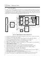
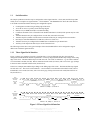
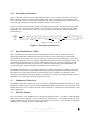
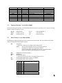
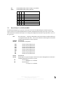
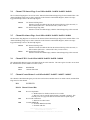
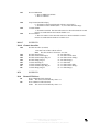
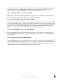
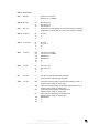
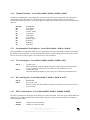
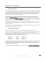
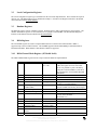
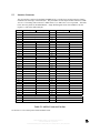
PMC-SIO4BX-SYNC
Hardware User’s Manual
HIGH SPEED
QUAD CHANNEL
SYNCHRONOUS SERIAL IO CONTROLLER
WITH DEEP TRANSMIT AND RECEIVE FIFOS
AND MULTIPROTOCOL TRANSCEIVERS
RS-485
RS-422 / V.11
RS-423 / V.10
RS-232 / V.28
General Standards Corporation
8302A Whitesburg Drive
Huntsville, AL 35802
Phone: (256) 880-8787
Fax: (256) 880-8788
URL: www.generalstandards.com
E-mail: [email protected]
Revision E
PREFACE
Revision History
1.
2.
3.
4.
5.
Rev A – Feb 2004 – Original rev from PCI-SIO4B manual.
Rev B – Misc Updates
Rev C – Aug 2004 - Misc Updates
Rev D – Jun 2005 – update for v404 firmware
Rev E – Nov 2007 – update for v40C firmware
Additional copies of this manual or other General Standards Corporation literature may be obtained
from:
General Standards Corporation
8302A Whitesburg Drive
Huntsville, Alabama 35802
Telephone: (256) 880-8787
Fax: (256) 880-8788
URL: www.generalstandards.com
The information in this document is subject to change without notice.
General Standards Corporation makes no warranty of any kind with regard to this material, including,
but not limited to, the implied warranties of merchantability and fitness for a particular purpose. Although
extensive editing and reviews are performed before release to ECO control, General Standards
Corporation assumes no responsibility for any errors that may exist in this document. No commitment is
made to update or keep current the information contained in this document.
General Standards Corporation does not assume any liability arising out of the application or use of
any product or circuit described herein, nor is any license conveyed under any patent right of any rights of
others.
General Standards Corporation assumes no responsibility resulting from omissions or errors in this
manual, or from the use of information contained herein.
General Standards Corporation reserves the right to make any changes, without notice, to this product
to improve reliability, performance, function, or design.
All rights reserved
No parts of this document may be copied or reproduced in any form or by any means without prior written
consent of General Standards Corporation.
Copyright © 2007 General Standards Corporation
RELATED PUBLICATIONS
PLX PCI 9080 Data Book
PLX Technology Inc.
390 Potrero Avenue
Sunnyvale, CA 4085
(408) 774-3735
http://www.plxtech.com/
EIA-422-A – Electrical Characteristics of Balanced Voltage Digital Interface Circuits
(EIA order number EIA-RS-422A)
EIA-485 – Standard for Electrical Characteristics of Generators and Receivers for Use in Balanced Digital
Multipoint Systems
(EIA order number EIA-RS-485)
EIA Standards and Publications can be purchased from:
GLOBAL ENGINEERING DOCUMENTS
15 Inverness Way East
Englewood, CO 80112
Phone: (800) 854-7179
http://global.ihs.com/
PCI Local Bus Specification Revision 2.1 June 1, 1995.
Copies of PCI specifications available from:
PCI Special Interest Group
NE 2575 Kathryn Street, #17
Hillsboro, OR 97124
http://www.pcisig.com/
TABLE OF CONTENTS
CHAPTER 1: INTRODUCTION .............................................................................................................................1
1
1.1
1.1.1
1.1.2
1.2
1.3
1.4
1.5
1.6
GENERAL DESCRIPTION..................................................................................................................................1
SERIAL INTERFACE .........................................................................................................................................2
THREE SIGNAL SERIAL INTERFACE.................................................................................................................2
TWO SIGNAL SERIAL INTERFACE....................................................................................................................3
DEEP TRANSMIT/RECEIVE FIFOS ...................................................................................................................3
MULTIPROTOCOL TRANSCEIVERS...................................................................................................................3
PMC/PCI INTERFACE .....................................................................................................................................3
GENERAL PURPOSE IO ...................................................................................................................................4
CONNECTOR INTERFACE.................................................................................................................................4
CHAPTER 2: LOCAL SPACE REGISTERS .........................................................................................................5
2
2.1
2.2
2.3
2.4
2.5
2.6
2.7
2.8
2.8.1
2.8.2
2.8.3
2.8.4
2.9
2.10
2.11
2.12
2.13
2.14
2.15
2.16
GSC FIRMWARE (LOCAL SPACE) REGISTERS .................................................................................................5
FIRMWARE REVISION: LOCAL OFFSET 0X0000..............................................................................................6
BOARD CONTROL: LOCAL OFFSET 0X0004 ...................................................................................................6
BOARD STATUS: LOCAL OFFSET 0X0008 .......................................................................................................8
CHANNEL TX ALMOST FLAGS: LOCAL OFFSET 0X0010 / 0X0020 / 0X0030 / 0X0040....................................9
CHANNEL RX ALMOST FLAGS: LOCAL OFFSET 0X0014 / 0X0024 / 0X0034 / 0X0044 ....................................9
CHANNEL FIFO: LOCAL OFFSET 0X0018 / 0X0028 / 0X0038 / 0X0048 ..........................................................9
CHANNEL CONTROL/STATUS: LOCAL OFFSET 0X001C / 0X002C / 0X003C / 0X004C ...................................9
INTERRUPT REGISTERS .................................................................................................................................11
INTERRUPT CONTROL: LOCAL OFFSET 0X0060 ...........................................................................................12
INTERRUPT STATUS/CLEAR: LOCAL OFFSET 0X0064 ..................................................................................12
INTERRUPT EDGE/LEVEL: LOCAL OFFSET 0X0068 ......................................................................................12
INTERRUPT HI/LO: LOCAL OFFSET 0X006C ................................................................................................12
CHANNEL PIN SOURCE: LOCAL OFFSET 0X0080 / 0X0084 / 0X0088 / 0X008C ............................................13
CHANNEL PIN STATUS: LOCAL OFFSET 0X0090 / 0X0094 / 0X0098 / 0X009C.............................................15
PROGRAMMABLE CLOCK REGISTERS: LOCAL OFFSET 0X00A0 / 0X00A4 / 0X00A8 ...................................15
TX COUNT REGISTER: LOCAL OFFSET 0X00B0 / 0X00B4 / 0X00B8 / 0XBC................................................15
RX COUNT REGISTER: LOCAL OFFSET 0X00C0 / 0X00C4 / 0X00C8 / 0XCC................................................15
FIFO COUNT REGISTER: LOCAL OFFSET 0X00D0 / 0X00D4 / 0X00D8 / 0X00DC .......................................15
FIFO SIZE REGISTER: LOCAL OFFSET 0X00E0 / 0X00E4 / 0X00E8 / 0X00EC .............................................16
FEATURES REGISTER: LOCAL OFFSET 0X00FC............................................................................................16
CHAPTER 3: PCI INTERFACE............................................................................................................................17
3
3.1
3.2
3.3
3.4
3.4.1
PCI INTERFACE REGISTERS ..........................................................................................................................17
PCI CONFIGURATION REGISTERS .................................................................................................................17
LOCAL CONFIGURATION REGISTERS ............................................................................................................18
RUNTIME REGISTERS ....................................................................................................................................18
DMA REGISTERS .........................................................................................................................................18
DMA CHANNEL MODE REGISTER: (PCI 0X80 / 0X94) .................................................................................18
CHAPTER 4: PROGRAMMING...........................................................................................................................19
4.1
4.1.1
4.1.2
4.1.3
4.1.4
4.1.5
4.1.6
4.2
4.2.1
SERIAL INTERFACE .......................................................................................................................................19
SERIAL INTERFACE DEFINITION....................................................................................................................19
TWO SIGNAL INTERFACE ..............................................................................................................................19
TX BIT COUNT / TX GAP ..............................................................................................................................19
RX BIT COUNT .............................................................................................................................................20
DCE/DTE MODE .........................................................................................................................................20
LOOPBACK MODES .......................................................................................................................................20
FIFOS ..........................................................................................................................................................21
FIFO FLAGS .................................................................................................................................................21
4.2.2
4.2.3
4.3
4.4
4.5
4.6
4.7
FIFO COUNTERS ..........................................................................................................................................21
INTERNAL VS. EXTERNAL FIFOS ..................................................................................................................22
BOARD VS CHANNEL REGISTERS ..................................................................................................................22
GENERAL PURPOSE IO .................................................................................................................................22
INTERRUPTS .................................................................................................................................................22
PROGRAMMABLE OSCILLATOR / PROGRAMMABLE CLOCKS .........................................................................23
PCI DMA.....................................................................................................................................................23
CHAPTER 5: HARDWARE CONFIGURATION ...............................................................................................24
5
5.1
5.2
5.3
BOARD LAYOUT ...........................................................................................................................................24
BOARD ID JUMPER J5...................................................................................................................................24
INTERFACE CONNECTOR...............................................................................................................................25
RS485/RS422 TERMINATION RESISTORS ...............................................ERROR! BOOKMARK NOT DEFINED.
CHAPTER 6: ORDERING OPTIONS ..................................................................................................................26
6
6.1
6.2
6.3
6.4
ORDERING INFORMATION .............................................................................................................................26
BOARD ORDERING OPTION – FIFO SIZE ......................................................................................................26
INTERFACE CABLE .......................................................................................................................................26
DEVICE DRIVERS ..........................................................................................................................................26
CUSTOM APPLICATIONS ...............................................................................................................................26
APPENDIX A: PROGRAMMABLE OSCILLATOR PROGRAMMING.........................................................27
PMC-SIO4BX-SYNC User Manual, Revision: E
General Standards Corporation
8302A Whitesburg Drive Huntsville, AL 35802, Phone: (256) 880-8787
IV
CHAPTER 1: INTRODUCTION
1
General Description
The General Standards PMC-SI04BX-SYNC board provides four, high-speed synchronous serial interface channels
for PMC applications. The SIO4BX-SYNC combines a flexible serial/parallel converter, deep FIFO data buffers,
and multiprotocol transceivers in four fully independent synchronous serial IO channels. These features, along with
four programmable baud rate generators and a high performance PMC/PCI interface engine, give the PMCSIO4BX-SYNC unsurpassed performance in a synchronous serial interface card.
x4 Channels
Rx
FIFO
Serial
to
Parallel
Multiprotocol
Transceiver
68 Pin
User
DTE
Tx
FIFO
PMC
Parallel
to
Serial
(Cable
IF)
DCE
PCI
Bridge
Control
Logic
Prog
Osc
Figure 1-1 Block Diagram of PMC-SIO4BX-SYNC
•
•
•
•
•
•
•
•
•
•
•
•
•
•
•
•
•
•
•
Four Multi-Protocol Synchronous Serial Channels with Separate Transmit and Receive Interfaces per Channel
Synchronous Serial Data Rates up to 10 Mbits/sec
Configurable for Two Signal (Clock and Data) or Three Signal (Clock, Data, and Envelope) Interface
Software Selectable RS-422/RS-485, RS-232, or RS-423 interface on a per channel basis
Fast RS422/RS485 Differential Cable Transceivers Provide Data Rate up to 10Mbps
RS423 and RS232 Cable Transceivers Provide Data Rate up to 230kbps
Independent Transmit and Receive FIFOs for Data Buffering for each Serial Channel – Up to 32k Deep Each
Configurable Polarity on all Serial Interface Signals.
NRZ and NRZB Data Encoding
Programmable Transmit Word Bit Count allows transmit word lengths from 1 to 64k bits.
Programmable Transmit Gap Bit Count allows number of clocks between words from 1 to 64k bits
Four Programmable Oscillators provides Baud Rate Clock generation from 10Mbps to 400bps
Bidirectional Signal Interface allows DTE or DCE configuration
Industry standard SCSI II type 68 pin front edge I/O Connector
Optional cable adapter splits 68 pin connectors into four separate DB25 connectors (one DB25 per channel).
Unused signals may be reconfigured as general purpose IO.
Dual PCI Master DMA Engine to speed transfers and minimize host I/O overhead
Easily mounted on PCI, cPCI, or PC104P carriers to provide multiprotocol support for other form factors.
A variety of device drivers are available, including VxWorks, WinNT, Win2k, Linux, and Labview
1.1
Serial Interface
The simple synchronous interface may be configured as a three signal interface - Clock, Data, and Envelope (Data
Valid), or an even simpler two signal interface – Clock and Data. The SIO4BX-SYNC allows the serial interface
to be further customized with the following user configurable options:
•
•
•
•
Clocking Data on either rising or falling edge of the clock.
Active Hi or Active Lo polarity for the Envelope Signal
NRZ (Level) or NRZB (Inverted Level) Data Encoding
Continuous Transmit Clock or Transmit Clock disabled when Data is invalid (Clock present only for valid
Data).
Transmit Word Size may be configured from 1 to 64k bits (consecutive bit count).
Transmit Gap Size (number of clocks between transmit words) may be configured from 0 to 64k bits
Data may be transmitted MSB first or LSB first (8-bit or less word size).
Transmit Clock may be configured from 10MHz down to 400Hz on a per channel basis
Auxiliary Clock Input from cable may be used as Transmit Clock
•
•
•
•
•
The following sections show some typical examples of how the SIO4BX-SYNC can be configured to support
different two and three signal interfaces.
1.1.1
Three Signal Serial Interface
Figure 1-2 shows two examples of typical 3-signal interfaces. The two diagrams show how the card can be
configured to handle different interface requirements. For the top diagram, Data and Envelope change on the rising
edge of the Clock. The Data and Envelope are both Active Hi. The Clock is continuous – e.g. the Clock continues
even when Data is Invalid (TxC Idl). Data is transmitted in 8 bit words (TxCount), with a two Clock ‘gap’ (TxGap)
in between each word (Data Valid for 8 bits, Invalid for 2).
In the lower example, Data and Envelope change on the falling edge of the Clock. The Data and Envelope signals
are both Active Lo. The Clock is still continuous – Clock continues even when Data is Invalid (TxC Idl). Data is
transmitted in 16 bit words (TxCount), with a one Clock ‘gap’ (TxGap) in between each word (Data Valid for 16
bits, Invalid for 1).
Clock
(Rising Edge)
Envelope
(Active Hi)
(Data)
(InValid)
(Data Valid)
Data
(NRZ)
'X'
'1'
'0'
'1'
'1'
'1'
'0'
'1'
'0'
'X'
(Data)
(InValid)
(Data Valid)
'X'
'1'
'1'
'1'
'1'
'1'
'1'
'0'
'X'
'X'
'0'
'0'
'1'
TxCount = 8, TxGap = 2, TxC Idl = 0
Clock
(Falling Edge)
Envelope
(Active Lo)
Data
(NRZB)
(Data Valid)
(Data Valid)
'X'
'X'
'1'
'1'
'0'
'1'
'0'
'1'
'0'
'0'
'0'
'1'
'0'
'1'
'0'
'0'
'1'
'0'
'X'
'1'
'1'
'1'
'1'
TxCount = 16, TxGap = 1, TxC Idl = 0
Figure 1-2 Three Signal Serial Interface
PMC-SIO4BX-SYNC User Manual, Revision: E
General Standards Corporation
8302A Whitesburg Drive Huntsville, AL 35802, Phone: (256) 880-8787
2
'0'
1.1.2
Two Signal Serial Interface
Figure 1-3 shows how the Clock can be used to qualify the Data to give a two signal serial interface. In this case,
Data is considered valid at every Clock. In this example, Data is Active Hi and changes on the rising edge of the
Clock. The Clock is not present when Data is invalid.(TxC Idl). Data is transmitted in 8 bit words (TxCount), with
a two clock ‘gap’ (TxGap) in between each word (Data Valid for 8 bits, Invalid for 2).
In the lower example, Data and Envelope change on the falling edge of the Clock. The Data and Envelope signals
are both Active Lo. The clock is still continuous – Clock continues even when Data is Invalid (TxC Idl). Data is
transmitted in 16 bit words (TxCount), with a one Clock ‘gap’ (TxGap) in between each word (Data Valid for 16
bits, Invalid for 1).
Clock
(Rising Edge)
Data
(NRZ)
'X'
'0'
'0'
'1'
'0'
'1'
'0'
'1'
'1'
'1'
'0'
'1'
'0'
'1'
'1'
'0'
'1'
'X'
'0'
'0'
'0'
'0'
'1'
TxCount = 16, TxGap = 1, TxC Idl = 1
Figure 1-3 Two Signal Serial Interface
1.2
Deep Transmit/Receive FIFOs
Data is transferred to/from the serial interface through Transmit and Receive FIFOs. Each of the four serial
channels has an independent Transmit FIFO and a Receive FIFO for a total of eight separate on-board FIFOs.
These FIFOs can be one of three sizes: 512 bytes, 8 kbytes, or 32 kbytes (based on ordering option). FIFOs allow
data transfer to continue to/from the IO interface independent of PCI interface transfers and software overhead. The
required FIFO size may depend on several factors including data transfer size, required throughput rate, and the
software overhead (which will also vary based on OS). Generally, faster baud rates (greater than 500kbps) will
require deeper FIFOs. Deeper FIFOs help ensure no data is lost for critical systems.
The SIO4BX-SYNC provides access to complete FIFO status to optimize data transfers. In addition to Empty and
Full indicators, each FIFO has a programmable Almost Empty Flag and a programmable Almost Full Flag. These
FIFO flags may be used as interrupt sources to monitor FIFO fill levels. In addition, real-time FIFO counters
showing the exact number of words in the FIFO are also provided for each FIFO. By utilizing these FIFO counters,
data transfers can be optimized to efficiently send and receive data.
1.3
Multiprotocol Transceivers
The SIO4BX-SYNC Data is transferred over the user interface using high-speed multiprotocol transceivers. These
multiprotocol transceivers are software selectable as RS422/RS485, RS423, or RS232 on a per channel basis. Each
channel direction may also be configured as DTE or DCE configuration. This allows for either full duplex or half
duplex configurations.
1.4
PMC/PCI Interface
The control interface to the SIO4BX-SYNC is through the PMC/PCI interface. An industry standard PCI9080
bridge chip from PLX Technology is used to implement PCI Specification 2.1. The PCI9080 provides the 32bit,
33MHz (132MBit/sec) interface between the PCI bus and the Local 32 bit bus. It also provides for high-speed
DMA transfers to efficiently move data to and from the board.
PMC-SIO4BX-SYNC User Manual, Revision: E
General Standards Corporation
8302A Whitesburg Drive Huntsville, AL 35802, Phone: (256) 880-8787
3
'1'
1.5
General Purpose IO
Since some signals may not be used in all applications, the SIO4BX provides the flexibility to configure all signals
to be used as general purpose IO. Each channel also contains two dedicated General Purpose IO signals –
TxSp/RxSp and TxAuxC/RxAuxC. In addition, all output signals may be forced to a Hi or Lo state. This also
allows signals from unused channels to be available as general purpose IO.
1.6
Connector Interface
The SIO4BX provides a user IO interface through a front-side card edge connector. All four serial channels
interface through this high-density, 68 pin SCSI II type connector, and are grouped to simplify separating the cable
into four distinct serial connectors.
Standard cables are available from General Standards in various lengths to adapt the single 68 pin SCSII connector
into four DB25 connectors (one per channel). A standard cable is also available with a single 68 pin SCSII
connector on one end and open on the other. This allows the user to add a custom connector (or connect to a
terminal block). General Standards will also work with customers to fabricate custom cables. Consult factory for
details on custom cables.
PMC-SIO4BX-SYNC User Manual, Revision: E
General Standards Corporation
8302A Whitesburg Drive Huntsville, AL 35802, Phone: (256) 880-8787
4
CHAPTER 2: LOCAL SPACE REGISTERS
2
GSC Firmware (Local Space) Registers
The PMC-SIO4BX-SYNC is accessed through two sets of registers – PCI Registers and GSC Firmware Registers.
The GSC Firmware Registers (referred to as Local Space Registers), which provide the control/status for the
SIO4BX-SYNC board, are described below. The PCI registers (internal to the PLX 9080 PCI controller) are
discussed in Chapter 3.
Offset Address
Size
Access*
0x0000
0x0004
0x0008
0x000C
0x0010
0x0014
0x0018
0x001C
0x0020
0x0024
0x0028
0x002C
0x0030
0x0034
0x0038
0x003C
0x0040
0x0044
0x0048
0x004C
0x0060
0x0064
0x0068
0x006C
0x0070-0x007C
0x0080
0x0084
0x0088
0x008C
0x0090
0x0094
0x0098
0x009C
0x00A0
0x00A4
0x00A8
0x00AC
0x00B0
0x00B4
0x00B8
0x00BC
0x00C0
0x00C4
0x00C8
D32
D32
D32
-D32
D32
D32
D32
D32
D32
D32
D32
D32
D32
D32
D32
D32
D32
D32
D32
D32
D32
D32
D32
--D32
D32
D32
D32
D32
D32
D32
D32
D32
D32
D32
--D32
D32
D32
D32
D32
D32
D32
Read Only
Read/Write
Read Only
-Read/Write
Read/Write
Read/Write
Read/Write
Read/Write
Read/Write
Read/Write
Read/Write
Read/Write
Read/Write
Read/Write
Read/Write
Read/Write
Read/Write
Read/Write
Read/Write
Read/Write
Read/Write
Read Only
Read/Write
-Read/Write
Read/Write
Read/Write
Read/Write
Read Only
Read Only
Read Only
Read Only
Read/Write
Read/Write
Read/Write
-Read/Write
Read/Write
Read/Write
Read/Write
Read/Write
Read/Write
Read/Write
Register Name
Firmware Revision
Board Control
Board Status
Reserved
Ch 1 Tx Almost Full/Empty
Ch 1 Rx Almost Full/Empty
Ch l Data FIFO
Ch 1 Control/Status
Ch 2 Tx Almost Full/Empty
Ch 2 Rx Almost Full/Empty
Ch 2 Data FIFO
Ch 2 Control/Status
Ch 3 Tx Almost Full/Empty
Ch 3 Rx Almost Full/Empty
Ch 3 Data FIFO
Ch 3 Control/Status
Ch 4 Tx Almost Full/Empty
Ch 4 Rx Almost Full/Empty
Ch 4 Data FIFO
Ch 4 Control/Status
Interrupt Control
Interrupt Status/Clear
Interrupt Edge/Level
Interrupt High/Low
RESERVED
Ch 1Pin Source
Ch 2 Pin Source
Ch 3 Pin Source
Ch 4 Pin Source
Ch 1Pin Status
Ch 2 Pin Status
Ch 3 Pin Status
Ch 4 Pin Status
Programmable Osc RAM Addr
Programmable Osc RAM Data
Programmable Osc Control/Status
RESERVED
Ch1 TxCount / TxGap
Ch2 TxCount / TxGap
Ch3 TxCount / TxGap
Ch4 TxCount / TxGap
Ch1 RxCount
Ch2 RxCount
Ch3 RxCount
PMC-SIO4BX-SYNC User Manual, Revision: E
General Standards Corporation
8302A Whitesburg Drive Huntsville, AL 35802, Phone: (256) 880-8787
Default Value (Hex)
C21104XX
00000000
000000XX
00000000
00070007
00070007
000000XX
0000CC00
00070007
00070007
000000XX
0000CC00
00070007
00070007
000000XX
0000CC00
00070007
00070007
000000XX
0000CC00
00000000
00000000
FFFFFFFF
FFFFFFFF
-------00000020
00000020
00000020
00000020
000000XX
000000XX
000000XX
000000XX
00000000
00000000
00000000
-------00000000
00000000
00000000
00000000
00000000
00000000
00000000
5
0x00CC
0x00D0
0x00D4
0x00D8
0x00DC
0x00E0
0x00E4
0x00E8
0x00EC
0x00F0-0x00F8
0x00FC
2.1
D32
D32
D32
D32
D32
D32
D32
D32
D32
--D32
Read/Write
Read Only
Read Only
Read Only
Read Only
Read Only
Read Only
Read Only
Read Only
-Read Only
Ch4 RxCount
Ch1 FIFO Count
Ch2 FIFO Count
Ch3 FIFO Count
Ch4 FIFO Count
Ch1 FIFO Size
Ch2 FIFO Size
Ch3 FIFO Size
Ch4 FIFO Size
RESERVED
Features Register
00000000
00000000
00000000
00000000
00000000
XXXXXXXX
XXXXXXXX
XXXXXXXX
XXXXXXXX
-------000000XX
Firmware Revision: Local Offset 0x0000
The Firmware ID register provides version information about the firmware on the board. This is useful for technical
support to identify the firmware version.
D31:16
D15:8
D7:0
2.2
HW Board Rev
Firmware Type ID
Firmware Revision
0xC211
0x04
XX
PMC-SIO4BX Rev A
Sync Firmware
Firmware Version
Board Control: Local Offset 0x0004
The Board Control Register defines the general control functions for the board. The main function in this register
defines the Demand mode DMA channel requests.
D31
Board Reset
1 = Reset all Local Registers and FIFOs to their default values
Notes:
This bit will automatically clear to 0 following the board reset.
Board Reset will NOT reset programmable oscillator.
Following a Board Reset, ResetInProgress bit (D31) of the Board Status
Register will remain set until the Board reset is complete;
D30
D29:9
D8
RESERVED (Debug Internal FIFO)
RESERVED
Rx FIFO Stop on Full
1 = If Rx FIFO becomes full, stop receiving data (disable receiver).
Demand Mode DMA Channel 1 Single Cycle Disable
Demand Mode DMA Channel 1 Request
D7
D6:4
D
6
0
1
0
1
0
1
0
1
D
5
0
0
1
1
0
0
1
1
D
4
0
0
0
0
1
1
1
1
Demand Mode DMA 1 Channel
Channel 1 Rx
Channel 1 Tx
Channel 2 Rx
Channel 2 Tx
Channel 3 Rx
Channel 3 Tx
Channel 4 Rx
Channel 4 Tx
PMC-SIO4BX-SYNC User Manual, Revision: E
General Standards Corporation
8302A Whitesburg Drive Huntsville, AL 35802, Phone: (256) 880-8787
6
PMC-SIO4BX-SYNC User Manual, Revision: E
General Standards Corporation
8302A Whitesburg Drive Huntsville, AL 35802, Phone: (256) 880-8787
7
D3
D2:0
Demand Mode DMA Channel 0 Single Cycle Disable
Demand Mode DMA Channel 0 Request
D
2
0
1
0
1
0
1
0
1
2.3
D
1
0
0
1
1
0
0
1
1
D
0
0
0
0
0
1
1
1
1
Demand Mode DMA 0 Channel
Channel 1 Rx
Channel 1 Tx
Channel 2 Rx
Channel 2 Tx
Channel 3 Rx
Channel 3 Tx
Channel 4 Rx
Channel 4 Tx
Board Status: Local Offset 0x0008
The Board Status Register gives general overall status for a board. The Board Jumpers (D1:D0) are physical
jumpers which can be used to distinguish between boards if multiple SIO4 boards are present in a system. Most
other information contained in this register is for debug and configuration information only and will have no use to
the typical user.
D31
D30:D16
D15:D8
D15
D14
D13
D12
D11
D10
D9
D8
D7:D2
D1:D0.
D1
D0
Reset In Progress – following a Board Reset, this bit will remain set while the FIFO size
is being detected (less than 2ms). No accesses (other than monitoring this bit) should be
attempted until the Board reset has completed.
RESERVED
External FIFO Configuration
External Ch4 Rx FIFO Present
External Ch4 Tx FIFO Present
External Ch3 Rx FIFO Present
External Ch3 Tx FIFO Present
External Ch2 Rx FIFO Present
External Ch2 Tx FIFO Present
External Ch1 Rx FIFO Present
External Ch1 Tx FIFO Present
RESERVED
Board Jumpers are physical jumpers which can be used to distinguish between boards if
multiple SIO4 boards are present in a system.
Board Jumper 1
0 = Jumper J5:3-4 installed
Board Jumper 0
0 = Jumper J5:1-2 installed
PMC-SIO4BX-SYNC User Manual, Revision: E
General Standards Corporation
8302A Whitesburg Drive Huntsville, AL 35802, Phone: (256) 880-8787
8
2.4
Channel TX Almost Flags: Local Offset 0x0010 / 0x0020 / 0x0030 / 0x0040
The Tx Almost Flag Registers are used to set the Almost Full and Almost Empty Flags for the transmit FIFOs. The
Almost Full/Empty Flags may be read as status bits in the Channel Control/Status Register, and are also edgetriggered interrupt sources to the Interrupt Register.
D31:16
D15:0
2.5
TX Almost Full Flag Value
Number of words from FIFO Full when the Almost Full Flag will be asserted (i.e.
FIFO contains{FIFO Size – Almost Full Value} words or more.)
TX Almost Empty Flag Value
Number of words from FIFO Empty when the Almost Empty Flag will be asserted.
Channel Rx Almost Flags: Local Offset 0x0014 / 0x0024 / 0x0034 / 0x0044
The Rx Almost Flag Registers are used to set the Almost Full and Almost Empty Flags for the transmit FIFOs. The
Almost Full/Empty Flags may be read as status bits in the Channel Control/Status Register, and are also edgetriggered interrupt sources to the Interrupt Register.
D31:16
D15:0
2.6
RX Almost Full Flag Value
Number of words from FIFO Full when the Almost Full Flag will be asserted (i.e.
FIFO contains {FIFO Size – Almost Full Value} words or more.)
RX Almost Empty Flag Value
Number of words from FIFO Empty when the Almost Empty Flag will be asserted
Channel FIFO: Local Offset 0x0018 / 0x0028 / 0x0038 / 0x0048
The Channel FIFO Register passes serial data to/from the serial controller. The same register is used to access both
the Transmit FIFO (writes) and Receive FIFO (reads).
D31:8
D7:0
2.7
RESERVED
Channel FIFO Data
Channel Control/Status: Local Offset 0x001C / 0x002C / 0x003C / 0x004C
The Channel Control/Status Register provides the reset functions and data transceiver enable controls, and the FIFO
Flag status for each channel.
D31
RESERVED
D30:24 Channel Control Bits
D30
D29
D28
Receive Gap Enable
0 = Bit D24 (Receive Enable) controls receiver enable
1 = Receiver won’t be started unless Bit D24=1 and RxE is negated. This
basically waits for a gap in the data stream before data reception begins.
Receive Bit Count Reset
1 = Reset Receive Bit Counter
Transmit MSB/LSB
0 = Transmit MSB first (default)
1 = Transmit LSB first
PMC-SIO4BX-SYNC User Manual, Revision: E
General Standards Corporation
8302A Whitesburg Drive Huntsville, AL 35802, Phone: (256) 880-8787
9
D27
Receive MSB/LSB
0 = Receive MSB first (default)
1 = Receive LSB first
D26
Stop Transmit On FIFO Empty
0 = Transmitter remains enabled under software control (D17)
1 = Transmitter will be disabled (D25 = ‘0’) if Tx FIFO becomes empty
Transmit Enable
1 = Transmitter enabled. Note that cable transceiver direction should be set and
transceivers enabled before the Transmit Enable is set.
Receive Enable
1 = Receiver enabled. Note that cable transceiver direction should be set and
transceivers enabled before the Receive Enable is set.
D25
D24
D23:17
RESERVED
D16:8 Channel Status Bits
D16
D15
D14
D13
D12
D11
D10
D9
D8
D7:2
D1:0
D1
D0
Rx FIFO Overflow (Latched)
1= Rx Data was lost due to Rx Overflow.
Note: This bit is latched. Write D16=1 to clear.
Rx FIFO Full Flag Lo
(0 = Rx FIFO Full)
Rx FIFO Almost Full Flag Lo
(0 = Rx FIFO Almost Full)
Rx FIFO Almost Empty Flag Lo
(0 = Rx FIFO Almost Empty)
Rx FIFO Empty Flag Lo
(0 = Rx FIFO Empty)
Tx FIFO Full Flag Lo
(0 = Tx FIFO Full)
Tx FIFO Almost Full Flag Lo
(0 = Tx FIFO Almost Full)
Tx FIFO Almost Empty Flag Lo
(0 = Tx FIFO Almost Empty)
Tx FIFO Empty Flag Lo
(0 = Tx FIFO Empty)
RESERVED
Channel FIFO Reset
Reset Channel Rx FIFO (Pulsed)
Note: This value will automatically clear to ‘0’.
Reset Channel Tx FIFO (Pulsed)
Note: This value will automatically clear to ‘0’.
PMC-SIO4BX-SYNC User Manual, Revision: E
General Standards Corporation
8302A Whitesburg Drive Huntsville, AL 35802, Phone: (256) 880-8787
10
2.8
Interrupt Registers
There are 32 on-board interrupt sources (in addition to PLX interrupts), each of which may be individually enabled.
Four interrupt registers control the on-board interrupts – Interrupt Control, Interrupt Status, Interrupt Edge/Level,
and Interrupt Hi/Lo. The Interrupt sources are:
IRQ #
IRQ0
IRQ1
IRQ2
IRQ3
IRQ4
IRQ5
IRQ6
IRQ7
IRQ8
IRQ9
IRQ10
IRQ11
IRQ12
IRQ13
IRQ14
IRQ15
IRQ16
IRQ17
IRQ18
IRQ19
IRQ20
IRQ21
IRQ22
IRQ23
IRQ24
IRQ25
IRQ26
IRQ27
IRQ28
IRQ29
IRQ30
IRQ31
Source
Ch1 RxE
Ch1 Tx FIFO Almost Empty
Ch1 Rx FIFO Almost Full
Ch1 RxSp
Ch2 RxE
Ch2 Tx FIFO Almost Empty
Ch2 Rx FIFO Almost Full
Ch2 RxSp
Ch3 RxE
Ch3 Tx FIFO Almost Empty
Ch3 Rx FIFO Almost Full
Ch3 RxSp
Ch4 RxE
Ch4 Tx FIFO Almost Empty
Ch4 Rx FIFO Almost Full
Ch4 RxSp
Ch1 Tx FIFO Empty
Ch1 Tx FIFO Full
Ch1 Rx FIFO Empty
Ch1 Rx FIFO Full
Ch2 Tx FIFO Empty
Ch2 Tx FIFO Full
Ch2 Rx FIFO Empty
Ch2 Rx FIFO Full
Ch3 Tx FIFO Empty
Ch3 Tx FIFO Full
Ch3 Rx FIFO Empty
Ch3 Rx FIFO Full
Ch4 Tx FIFO Empty
Ch4 Tx FIFO Full
Ch4 Rx FIFO Empty
Ch4 Rx FIFO Full
Default Level
Rising Edge
Rising Edge
Rising Edge
Rising Edge
Rising Edge
Rising Edge
Rising Edge
Rising Edge
Rising Edge
Rising Edge
Rising Edge
Rising Edge
Rising Edge
Rising Edge
Rising Edge
Rising Edge
Rising Edge
Rising Edge
Rising Edge
Rising Edge
Rising Edge
Rising Edge
Rising Edge
Rising Edge
Rising Edge
Rising Edge
Rising Edge
Rising Edge
Rising Edge
Rising Edge
Rising Edge
Rising Edge
Alternate Level
Falling Edge
Falling Edge
Falling Edge
Falling Edge
Falling Edge
Falling Edge
Falling Edge
Falling Edge
Falling Edge
Falling Edge
Falling Edge
Falling Edge
Falling Edge
Falling Edge
Falling Edge
Falling Edge
Falling Edge
Falling Edge
Falling Edge
Falling Edge
Falling Edge
Falling Edge
Falling Edge
Falling Edge
Falling Edge
Falling Edge
Falling Edge
Falling Edge
Falling Edge
Falling Edge
Falling Edge
Falling Edge
For all interrupt registers, the IRQ source (IRQ31:IRQ0) will correspond to the respective data bit (D31:D0) of each
register. (D0 = IRQ0, D1 = IRQ1, etc.)
All FIFO interrupts are edge triggered active high. This means that an interrupt will be asserted (assuming it is
enabled) when a FIFO Flag transitions from FALSE to TRUE (rising edge triggered) or TRUE to FALSE (falling
edge). For example: If Tx FIFO Empty Interrupt is set for Rising Edge Triggered, the interrupt will occur when the
FIFO transitions from NOT EMPTY to EMPTY. Likewise, if Tx FIFO Empty Interrupt is set as Falling Edge
Triggered, the interrupt will occur when the FIFO transitions from EMPTY to NOT EMPTY.
PMC-SIO4BX-SYNC User Manual, Revision: E
General Standards Corporation
8302A Whitesburg Drive Huntsville, AL 35802, Phone: (256) 880-8787
11
All Interrupt Sources share a single interrupt request back to Local Interrupt Input of the PCI9080 PLX chip. This
Local Interrupt input must be enabled in the PLX Interrupt Control/Status Register to be recognized as a PCI
interrupt source. See Section 4.4 Interrupts for further interrupt programming information.
2.8.1
Interrupt Control: Local Offset 0x0060
The Interrupt Control register individually enables each interrupt source. A ‘1’ enables each interrupt source; a ‘0’
disables. An interrupt source must be enabled for an interrupt to be generated.
2.8.2
Interrupt Status/Clear: Local Offset 0x0064
The Interrupt Status Register shows the status of each respective interrupt source. If an interrupt source is enabled
in the Interrupt Control Register, a ‘1’ in the Interrupt Status Register indicates the respective interrupt has occurred.
The interrupt source will remain latched until the interrupt is cleared, either by writing to the Interrupt Status/Clear
Register with a ‘1’ in the respective interrupt bit position, or the interrupt is disabled in the Interrupt Control
Register. Clearing an interrupt which is not enabled or not asserted will have no effect.
2.8.3
Interrupt Edge/Level: Local Offset 0x0068
The Interrupt Edge Register is an information only (read only) register. This register can be used by a generic
driver to determine if the interrupt source is edge or level triggered. All interrupt sources on the SIO4BX-SYNC
are edge triggered.
2.8.4
Interrupt Hi/Lo: Local Offset 0x006C
The Interrupt Edge Register is an information only register which denotes all interrupt sources as edge triggered.
The Interrupt Hi/Lo Register define each interrupt source as rising edge or falling edge. For example, a rising edge
of the TX Empty source will generate an interrupt when the TX FIFO becomes empty. Defining the source as
falling edge will trigger an interrupt when the TX FIFO becomes “NOT Empty”.
PMC-SIO4BX-SYNC User Manual, Revision: E
General Standards Corporation
8302A Whitesburg Drive Huntsville, AL 35802, Phone: (256) 880-8787
12
2.9
Channel Pin Source: Local Offset 0x0080 / 0x0084 / 0x0088 / 0x008C
The Channel Pin Source Register configures the function of the cable interface signals as well as controls the
transceiver protocols.
31
30
29
28
Cable Xcvr
Enable
X
Ext Loopback
Enable
DCE/DTE
Mode
23
Int
LB
22
21
XXX
20
19
18
TxD
Idl
X
17
16
RxD
Src
15
14
RxE
Src
27
13
RxC
Src
26
25
24
Transceiver Protocol Mode
12
11
TxSp
Src
10
9
TxAux
Src
8
7
6
TxD
Src
5
4
TxE
Src
3
TxC
Idl
2
1
0
TxC
Src
Pin Source Register
D31
Cable Transceiver Enable
Setting this bit turns on the cable transceivers. If this bit is cleared, the transceivers are tristated.
D30
RESERVED
D29
External Loopback Mode
When Cable Transceiver is enabled (Bit D31), this bit will automatically loopback the TxC/RxC,
TxD/RxD, and TxE/RxE signals at the cable (transceivers enabled).
Notes:
• The DCE/DTE mode will select the set of signals (DCE or DTE) to be looped back
D28
DCE/DTE Mode
This bit sets up the transceiver direction. Setting the mode to ‘1’ will enable DCE mode, while
‘0’ will set DTE mode (default). See Section 5.3 for a detail of the signal direction as defined for
each mode.
D27:24 Transceiver Protocol Mode
D27
0
0
0
0
0
1
D23
D26
0
0
0
0
1
X
Int LB
D25
0
0
1
1
X
X
D24
0
1
0
1
X
X
Transceiver Mode
RS-422 / RS-485
RS-423
RS-232
RESERVED
RESERVED
RESERVED
0
1
Normal Mode
Internal Loopback – TxC, TxD, TxE looped back internally
D22:21 RESERVED
D20
TxC Idl Lev
0
1
TxC driven low (‘0’) while Idle (Envelope Negated)
TxC driven high (‘1’) while Idle (Envelope Negated)
D19
TxD Idl Lev
0
1
TxD driven low (‘0’) while Idle (Envelope Negated)
TxD driven high (‘1’) while Idle (Envelope Negated)
PMC-SIO4BX-SYNC User Manual, Revision: E
General Standards Corporation
8302A Whitesburg Drive Huntsville, AL 35802, Phone: (256) 880-8787
13
D18:17 RESERVED
D16
RxD Src
0
1
RxD Active Hi (NRZ)
RxD Active Lo (NRZB)
00
01
1X
0
1
RxE Active Hi
RxE Active Lo
RxE Disabled
Sample Data on Falling Edge of Clock (Data Change on Rising)
Sample Data on Rising Edge of Clock (Data Change on Falling)
D12:11 TxSp Src
0X
10
11
Tri-State
'0'
'1'
D10:9
TxAuxC Src
00
01
10
11
Tri-State
Prg_Clk / 2
'0'
'1'
D8:6
TxD Src
000
001
01X
10X
110
111
TxD Active Hi (NRZ)
TxD Active Lo (NRZB)
RESERVED
RESERVED
'0'
'1'
D5:4
TxE Src
00
01
10
11
TxE Active Hi
TxE Active Lo
'0'
'1'
D3
TxC Idl
0
1
TxC driven while Idle (Envelope Negated)
No TxClk while Idle (Envelope Negated)
D2:0
TxC Src
000
Clock Data on Rising Edge of Internal Programmable Clock / 2
(Data/Envelope change on rising edge)
Clock Data on Falling Edge of Internal Programmable Clock / 2
(Data/Envelope change on falling edge)
Clock Data on Rising Edge of External Clock
(Data/Envelope change on rising edge)
Clock Data on Falling Edge of External Clock
(Data/Envelope change on falling edge)
RESERVED
'0'
'1'
D15:14 RxE Src
D13
RxC Src
001
010
011
10X
110
111
PMC-SIO4BX-SYNC User Manual, Revision: E
General Standards Corporation
8302A Whitesburg Drive Huntsville, AL 35802, Phone: (256) 880-8787
14
2.10
Channel Pin Status: Local Offset 0x0090 / 0x0094 / 0x0098 / 0x009C
In addition to standard inputs, unused inputs may be utilized as general purpose input signals. The Channel Pin
Status Register allows the input state of all the IO pins to be monitored. Output signals as well as inputs are
included to aid in debug operation. As the input signals are inputs from the cable, the transceivers must be enabled
before the
D31:D10
D9
D8
D7
D6
D5
D4
D3
D2
D1
D0
2.11
RESERVED
TxSp Output
RxSp Input
TxAuxC Output
TxE Output
TxD Output
TxC Output
RxAuxC Input
RxE Input
RxD Input
RxC Input
Programmable Clock Registers: Local Offset 0x00A0 / 0x00A4 / 0x00A8
The Programmable Clock Registers allow the user to program the on-board programmable oscillator and configure
the channel clock post-dividers. As GSC should provide software routines to program the clock, the user should
have no need to access these registers. See Section 4.6 for more information.
2.12
Tx Count Register: Local Offset 0x00B0 / 0x00B4 / 0x00B8 / 0xBC
D31:16
D15:0
2.13
Rx Count Register: Local Offset 0x00C0 / 0x00C4 / 0x00C8 / 0xCC
D31:16
D15:0
2.14
Gap Bit Count
When transmitting, these bits indicate the number of idle clocks between transmitted
words. To output a continuous stream of bits, this value should be set to zero.
Transmit Bit Count
These bits indicate the number of consecutive bits to transmit for each transmit word.
RESERVED
Receive Bit Count
When receiving, these bits indicate the number of consecutive bits received for the last
received word.
FIFO Count Register: Local Offset 0x00D0 / 0x00D4 / 0x00D8 / 0x00DC
The FIFO Count Registers display the current number of words in each FIFO. This value, along with the FIFO Size
Registers, may be used to determine the amount of data which can be safely transferred without over-running (or
under-running) the FIFOs.
D31:D16
D15:D0
Number of words in Rx FIFO
Number of words in Tx FIFO
PMC-SIO4BX-SYNC User Manual, Revision: E
General Standards Corporation
8302A Whitesburg Drive Huntsville, AL 35802, Phone: (256) 880-8787
15
2.15
FIFO Size Register: Local Offset 0x00E0 / 0x00E4 / 0x00E8 / 0x00EC
The FIFO Size Registers display the sizes of the installed data FIFOs. This value is calculated at power-up This
value, along with the FIFO Count Registers, may be used to determine the amount of data which can be safely
transferred without over-running (or under-running) the FIFOs.
D31:D16
D15:D0
2.16
Size of installed Rx FIFO
Size of installed Tx FIFO
Features Register: Local Offset 0x00FC
The Features Register allows software to account for added features in the firmware versions. Bits will be assigned
as new features are added.
D31:16
D15:8
D7:4
D3:0
RESERVED
Features Rev Level
0x7 - FIFO Counters/Size and Board Reset Feature implemented
0x3 - Programmable Clock Configuration = CY22393
PMC-SIO4BX-SYNC User Manual, Revision: E
General Standards Corporation
8302A Whitesburg Drive Huntsville, AL 35802, Phone: (256) 880-8787
16
CHAPTER 3: PCI INTERFACE
3
PCI Interface Registers
A PCI9080 I/O Accelerator from PLX Technology handles the PCI Interface. The PCI interface is compliant with
the 5V, 33MHz 32-bit PCI Specification 2.1. The PCI9080 provides dual DMA controllers for fast data transfers to
and from the on-board FIFOs. Fast DMA burst accesses provide for a maximum burst throughput of 132MB/s to
the PCI interface. To reduce CPU overhead during DMA transfers, the controller also implements Chained
(Scatter/Gather) DMA, as well as Demand Mode DMA.
Since many features of the PCI9080 are not utilized in this design, it is beyond the scope of this document to
duplicate the PCI9080 User’s Manual. Only those features, which will clarify areas specific to the PCI-X are
detailed here. Please refer to the PCI9080 User’s Manual (See Related Publications) for more detailed information.
Note that the BIOS configuration and software driver will handle most of the PCI9080 interface. Unless the user is
writing a device driver, the details of this PCI Interface Chapter may be skipped.
The PLX 9080 contains many registers, many of which have no effect on the SIO4BX performance. The following
section attempts to filter the information from the PCI9080 manual to provide the necessary information for a
SIO4BX specific driver.
The SIO4BX uses an on-board serial EEPROM to initialize many of the PCI9080 registers after a PCI Reset. This
allows board specific information to be preconfigured.
3.1
PCI Configuration Registers
The PCI Configuration Registers allow the PCI controller to identify and control the cards in a system.
PCI device identification is provided by the Vendor ID/Device ID (Addr 0x0000) and Sub-Vendor ID/Sub-Device
ID Registers (0x002C). The following definitions are unique to the General Standards SIO4BX boards. All
drivers should verify the ID/Sub-ID information before attaching to this card. These values are fixed via the Serial
EEPROM load following a PCI Reset, and cannot be changed by software.
Vendor ID
Device ID
Sub-Vendor ID
Sub-Device ID
0x10B5
0x9080
0x10B5
0x2401
PLX Technology
PCI9080
PLX Technology
GSC SIO4
The configuration registers also setup the PCI IO and Memory mapping for the SIO4BX. The PCI9080 is setup to
use PCIBAR0 and PCIBAR1 to map the internal PLX registers into PCI Memory and IO space respectively.
PCIBAR2 will map the Local Space Registers into PCI memory space, and PCIBAR3 is unused. Typically, the OS
will configure the PCI configuration space.
For further information of the PCI configuration registers, please consult the PLX Technology PCI9080 Manual.
PMC-SIO4BX-SYNC User Manual, Revision: E
General Standards Corporation
8302A Whitesburg Drive Huntsville, AL 35802, Phone: (256) 880-8787
17
3.2
Local Configuration Registers
The Local Configuration registers give information on the Local side implementation. These include the required
memory size. The SIO4 memory size is initialized to 4k Bytes. All other Local Registers initialize to the default
values described in the PCI9080 Manual.
3.3
Runtime Registers
The Runtime registers consist of mailbox registers, doorbell registers, and a general-purpose control register. The
mailbox and doorbell registers are not used and serve no purpose on the SIO4BX. All other Runtime Registers
initialize to the default values described in the PCI9080 Manual.
3.4
DMA Registers
The Local DMA registers are used to setup the DMA transfers to and from the on-board FIFOs. DMA is
supported only to the four FIFO locations. The SIO4BX supports both Demand (DREQ# controlled) and NonDemand mode DMA. Both Channel 0 and Channel 1 DMA are supported.
3.4.1
DMA Channel Mode Register: (PCI 0x80 / 0x94)
The DMA Channel Mode register must be setup to match the hardware implementation
Bit
D1:0
Description
Local Bus Width
Value
11 = 32 bit
00 = 8 bit
D5:2
D6
D7
D8
Internal Wait States
Ready Input Enable
Bterm# Input Enabled
Local Burst Enable
0000 = Unused
1 = Enabled
0 = Unused
1 = Supported
D9
D10
D11
D12
D13
D14
D15
D16
D17
D31:18
Chaining Enable (Scatter
Gather DMA)
Done Interrupt Enable
Local Addressing Mode
Demand Mode Enable
Write & Invalidate Mode
DMA EOT Enable
DMA Stop Data
Transfer Enable
DMA Clear Count Mode
DMA Channel Interrupt
Select
Reserved
X
X
1 = No Increment
X
Notes
Although the serial FIFOs only contain 8 bits
of data, the register access is still a 32bit
access. It is possible to “pack” the data by
setting the Local Bus Width to 8, but this is
only guaranteed to work with Non-Demand
Mode DMA
Bursting allows fast back-to-back accesses to
the FIFOs to speed throughput
DMA source addr, destination addr, and byte
count are loaded from memory in PCI Space.
DMA Done Interrupt
DMA to/from FIFOs only
Demand Mode DMA is supported for FIFO
accesses on the SIO4BX.
(See Section 3.3)
X
0 = Unused
0 = BLAST
terminates DMA
0 = Unused
X
0
PMC-SIO4BX-SYNC User Manual, Revision: E
General Standards Corporation
8302A Whitesburg Drive Huntsville, AL 35802, Phone: (256) 880-8787
18
CHAPTER 4: PROGRAMMING
4.1
Serial Interface
4.1.1
Serial Interface Definition
The Pin Source Register contains information which defines the physical serial interface. This register contains
fields to setup the polarity of the TxC, RxC, TxD, RxD, TxE, and RxE signals. As these signals are all individually
configurable, it is possible to setup the Receive channel differently than the Transmit channel. In addition, the TxD
Idle field defines the state of the TxD signal while idling (not sending data).
The MSB/LSB for both transmit and receive is setup in the Channel Control/Status register. Note that this acts only
upon the current byte. MSB will send/receive bit D7 first, LSB will send/receive D0 first. For word lengths of
other than 8 bits, the word should be right/left justified accordingly. Since the MSB/LSB only acts upon 8 bits, if
the bit length is greater than 8 bits, the bits will only be reversed on a byte by byte basis. The user may need to
rearrange bytes for bit lengths greater than 8 bits.
4.1.2
Two Signal Interface
A two signal interface is a special setup case of the three signal serial interface. In a three signal interface, an
envelope signal defines when data is valid. For a two wire case, every clock indicates valid data. When data is
invalid, the clock simply stops.
For transmit, the TxC Idle field defines the two signal interface. By setting the TxC Idle enable, the clock will stop
during idle periods. The TxCount and TxGap still apply. The TxE signal may be left enabled and simply
unconnected, or may be reconfigured as a general purpose output.
For receive, a two wire interface is defined when RxE is set as a general purpose input. When RxE is set as an
input, the internal logic simply assumes the internal RxE is always valid. Thus, all data is considered valid based on
the RxC clock.
4.1.3
Tx Bit Count / Tx Gap
The TxCount/TxGap register defines the number of consecutive bits to transmit in a word, as well as the number of
idle clock cycles between words. This configurability allows this board to interface with a custom user interface.
All data sent to/from the board is in 8 bit increments. Therefore, if TxCount is not a multiple of 8, all extra bits will
be padded with zeros. .For example, a TxCount of 14 would use 14 bits out of two consecutive bytes (and the two
extra bits would be ignored).
Note that there is no hardware interlock to ensure that TxCount bits are present in the Tx FIFO before a transmit can
begin. If TxCount is greater than 8 bits (and transmit is enabled), the first 8 bits will be transmitted as soon as it is
loaded into the TxFIFO. If the TxFIFO is empty when the first 8 bits complete, a gap will be inserted. Therefore, if
the TxCount is greater than 8 bits, some data should be preloaded into the TxFIFO before the transmit is enabled.
This will ensure a continuous data stream of the correct length.
For a continuous data stream, the TxCount should be set to 8 and TxGap to 0.
Certain TxCount/TxGap combinations may not work correctly in a very few instances. In general, a data word
cannot be transmitted or received faster than 500ns per byte. If the TxCount, TxGap, and serial data rate result in a
throughput rate of greater than 1 byte in 500ns, correct operation cannot be guaranteed. If an application requires
such an interface, please contact GSC tech support to determine if the board will work for your application.
PMC-SIO4BX-SYNC User Manual, Revision: E
General Standards Corporation
8302A Whitesburg Drive Huntsville, AL 35802, Phone: (256) 880-8787
19
4.1.4
Rx Bit Count
The Rx Bit Count is primarily a debug feature to check that the expected number of bits in a frame were received.
The Rx Bit Count will simply count received bits in the current frame. It will reset at the beginning of each frame
based on RxE, or may be reset via the Rx Bit Count Reset bit of the Channel Control Register. For a two signal
interface, this register will count all bits reveived.
4.1.5
DCE/DTE Mode
Since the main signal interface signals (Clock, Data, Envelope) are bidirectional signals, DTE/DCE mode is used to
control the direction of the cable interface for each signal set. The DTE/DCE mode bit in the Pin Source Register is
used to set the interface direction. Setting the channel mode to DTE or DCE will swap the location of the interface
signals on the connector (See Section 5.3 Interface Connector for cable pinout). By allowing the signal direction
(DTE or DCE) to be set via software control, the user can send and receive on a single set of bidirectional lines. If
bidirectional signals are not required, the mode should be set to DTE (default) and connected appropriately.
Note that the pin direction for the TxC/RxC, TxD/RxD, and TxE/RxE are always set by the DTE/DCE mode. If
these signals are used as GPIO (such as TxE and RxE in 2 wire mode), the IO direction is still set by the DTE/DCE
Mode – they are not individually configurable.
4.1.6
Loopback Modes
For normal operation, the Cable Transceiver Enable bit of the Pin Source Register will turn on the cable
transceivers, and the DTE/DCE Mode bit will set the transceiver direction. These bits must be set before any data is
transmitted over the user interface.
In addition, there are several ways to loopback data to aid in debug operations. Data may be physically looped
back externally by connecting one channel to another. For DB25 cable applications, this simple loopback method
will requires a gender changer to connect one channel to another. One channel will be set to DTE mode, the other
to DCE mode. Data sent from one channel will be received on the other.
An External Loopback mode (External Loopback bit set in the Pin Source Register) is also provided to loop back
data on the same channel without requiring any external cabling. In this mode, the DTE/DCE mode will control the
location for the transmit signals (TxC, TXD, TXD), and the receive signals will use these same signals as the
receive inputs. Since signals are transmitted and received through the transceivers, this mode allows the setup to be
verified (including signal polarity) without any external connections. Since the signals are driven at the
transceivers, any external connections could interfere with loopback operation. Therefore, the cable should be
disconnected when running in external loopback mode.
An Internal Loopback Mode is also provided which loops back on the same channel internal to the board. This
provides a loopback method which does not depend on DTE/DCE mode or signal polarity. This can remove cable
transceiver and signal setup issues to aid in debugging.. If the Cable Transceivers are enabled, the transmit data will
still appear on the appropriate transmit pins (based on DTE/DCE Mode setting). The Pin Status register will not
reflect internally looped back signals, only signals to/from the transceivers.
PMC-SIO4BX-SYNC User Manual, Revision: E
General Standards Corporation
8302A Whitesburg Drive Huntsville, AL 35802, Phone: (256) 880-8787
20
4.2
FIFOs
Deep transmit and receive FIFOs are the key to providing four high speed serial channels without losing data.
Several features have been implemented to help in managing the on-board FIFOs. These include FIFO flags
(Empty, Full, Almost Empty and Almost Full) presented as both real-time status bits and interrupt sources, and
individual FIFO counters to determine the exact FIFO fill level. DMA of data to/from the FIFOs provides for fast
and efficient data transfers.
A single memory address is used to access both transmit and receive FIFOs for each channel. Data written to this
memory location will be written to the transmit FIFO, and data read from this location retrieves data from the
receive FIFO. Individual resets for the FIFOs are also provided in the Channel Control/Status Register.
4.2.1
FIFO Flags
Four FIFO flags are present from each on-board FIFO: FIFO Empty, FIFO Full, FIFO Almost Empty, and FIFO
Almost Full. These flags may be checked at any time from the Channel Control/Status Register. Note these flags
are presented as active low signals (‘0’ signifies condition is true). The Empty and Full flags are asserted when the
FIFO is empty or full, respectively. The Almost Empty and Almost Full flags are software programmable such
that they may be asserted at any desired fill level. This may be useful in determining when a data transfer is
complete or to provide an indicator that the FIFO is in danger of overflowing and needs immediate service.
The Almost Flag value represents the number of bytes from each respective “end” of the FIFO. The Almost Empty
value represents the number of bytes from empty, and the Almost Full value represents the number of bytes from
full (NOT the number of bytes from empty). For example, the default value of “0x0007 0007” in the FIFO Almost
Register means that the Almost Empty Flag will indicate when the FIFO holds 7 bytes or fewer. It will transition as
the 8th byte is read or written. In this example, the Almost Full Flag will indicate that the FIFO contains (FIFO Size
– 7) bytes or more. For the standard 32Kbyte FIFO, an Almost Full value of 7 will cause the Almost Full flag to be
asserted when the FIFO contains 32761 (32k – 7) or more bytes of data .
The values placed in the FIFO Almost Registers take effect immediately, but should be set while the FIFO is empty
(or the FIFO should be reset following the change). Note that this is a little different than the method for FIFO
Flag programming which has previously been implemented on SIO4 boards. No FIFO programming delay is
necessary.
4.2.2
FIFO Counters
The FIFO Size and FIFO count registers can be used to determine the exact amount of data in a FIFO as well as the
amount of free space remaining in a FIFO. The size of each FIFO is auto-detected following a board reset. Realtime FIFO counters report the exact number of data words currently in each FIFO. By utilizing this information, the
user can determine the exact amount of data which can safely be transferred to the transmit FIFOs or transferred
from the receive FIFO. This information should help streamline data transfers by eliminating the need to
continuously check empty and full flags, yet still allow larger data blocks to be transferred.
4.2.3
FIFO Size
In some applications, 512byte FIFOs may be all that is required to implement a serial interface. This typically
includes baud rates slower than 500kbps, or applications where the transfer size is limited to less than 512 bytes at a
time (and an effective throughput rate less than 500kpbs). For these applications, a PMC-SIO4BX-SYNC-4KLC
board should be adequate. For faster applications, deeper external FIFO are required to ensure no data will be lost.
Please contact General Standards if you have any questions about determining which FIFO size may be necessary
for a specific application.
PMC-SIO4BX-SYNC User Manual, Revision: E
General Standards Corporation
8302A Whitesburg Drive Huntsville, AL 35802, Phone: (256) 880-8787
21
4.2.4
Internal vs. External FIFOs
In this manual, references may be made to internal and external FIFOs. There is really no difference between the
two as far as software is concerned. Internal FIFOs are simply small (512 byte) FIFOs which can be implemented
internal to the on-board FPGA to provide a lower cost board. From the user standpoint, there is no difference
between internal and external FIFOs. However, different firmware may be required. Therefore, certain status bits
may indicate internal or external FIFOs as a debug aid (if tech support issues arise).
4.3
Board vs. Channel Registers
Since four serial channels are implemented on a single board, some registers apply to the entire board, while others
are unique to each channel. It is intended that each channel can act independently, but the user must keep in mind
that certain accesses will affect the entire board. Typically, the driver will adequately handle keeping board and
channel interfaces separate. However, the user must also be mindful that direct access to certain registers will affect
the entire board, not just a specific channel.
The Board Control and Board Status registers provide board level controls. Fundamentally, a board reset will do
just that, reset all the GSC registers and FIFOs to their default state. Interrupt control is also shared among all
registers, although local bits are segregated by channel. The device driver should take care of appropriately
handling the inter-mixed channel interrupts and pass them on to the application appropriately.
4.4
General Purpose IO
Unused signals at the cable may be used for general purpose IO. The Pin Source and Pin Status Registers provide
for simple IO control of all the cable interface signals. For outputs, the output value is set using the appropriate
field in the Pin Source Register. All inputs can be read via the Pin Status register.
Since TxAuxC and RxAuxC share a single pin, the TxAuxC Src field in the Pin Source Register controls whether
AuxC will function as an input or output. If the field is set to ‘Tri-State’, the pin is set as RxAuxC Input.
Otherwise, The TxAuxC output will be driven (and the RxAuxC input will be equal to the TxAuxC output).
Likewise, the TxSp Src field in the Pin Source Register controls the Spare pin direction. If the field is set to ‘TriState’, RxSp will be an Input. Otherwise, RxSp will follow the TxSp output.
4.5
Interrupts
The PMC-SIO4BX-SYNC has a number of interrupt sources which are passed to the host CPU via the PCI IRQA.
Since there is only one physical interrupt source for the board, the interrupts pass through a number of “levels” to
get multiplexed onto this single interrupt. The interrupt originates in the PCI9080 PCI Bridge, which combines the
internal PLX interrupt sources (DMA) with the Local on-board interrupt. . The single Local Interrupt is made up of
the interrupt sources described in Section 2.8. The user should be aware that interrupts must be enabled at each
level for an interrupt to occur. For example, if a FIFO interrupt is used, it must be setup and enabled in the GSC
Firmware Interrupt Control Register, as well as enabled in the PCI9080. In addition, the interrupt must be
acknowledged and/or cleared at each level following the interrupt. The driver will typically take care of setting up
and handling the PCI9080 interrupts as well as most local interrupts. The specific driver manual should have more
information on how to handle these interrupts.
PMC-SIO4BX-SYNC User Manual, Revision: E
General Standards Corporation
8302A Whitesburg Drive Huntsville, AL 35802, Phone: (256) 880-8787
22
4.6
Programmable Oscillator / Programmable Clocks
The On-Board Programmable Oscillator provides each channel with a unique programmable clock source using a
Cypress Semiconductor CY22393 Programmable Clock generator. In order to program the oscillator, it is necessary
to calculate and program values for different clock frequencies. General Standards has developed routines to
calculate the necessary values for a given setup and program the clock generator. These clock setup routines have
been incorporated into most of the drivers.
The default clock configuration at power-up for the programmable clock on all channels is 20MHz. See Appendix
A for more detailed information concerning programming the on-board clock frequencies, as well as common
frequency setups. The specific driver manual should have information on clock setup. If not, please contact GSC
tech support for assistance.
4.7
PCI DMA
The PCI DMA functionality allows data to be transferred between host memory and the PCI-SIO4B onboard FIFOs
with the least amount of CPU overhead. The PCI9080 bridge chip handles all PCI DMA functions, and the device
driver should handle the details of the DMA transfer.
There are two PCI DMA modes – Non-Demand Mode DMA and Demand Mode DMA. In Non-Demand mode, all
data is transferred without data checks, so the driver must ensure no data will be lost. This adds a little software
overhead, but no data should be lost. For Demand mode, a hardware handshake is implemented such that the DMA
is throttled as the Tx FIFO becomes full or the Rx FIFO is empty. However, Demand Mode has some potential
drawbacks which could result in lost data. Given these tradeoffs, Non-Demand Mode DMA is the preferred method
for DMA transfers.
Non-Demand Mode DMA is fast, but it requires the driver to ensure there is enough data (receive) or space in the
FIFO (transmit) to ensure data will not be lost. Fortunately, the FIFO counters provide a real-time count of the
number of data bytes currently in the FIFO, so the driver should be able to break large transfers into smaller
transfers to ensure data is not lost. Although this adds a small bit of overhead, it can ensure that no data is lost.
With Demand Mode DMA, a large DMA transfer (greater than the size of the FIFO) can be setup, which requires
less software overhead. However, there are two potential drawbacks to this method. Firstly, if the transfer does not
complete, there is no way to determine how much data was actually transferred. This is primarily a problem for
receiving – the expected amount of data was never received. The workaround for this is to DMA the read data from
the RxFIFO in small blocks as it is received (the same as Non-Demand mode). The second problem is that the PCI
interface chip always wants to transfer 32bits at a time. Since the serial data is only 8bits, the Demand mode DMA
always wants to transfer 4 bytes (even if only 1 byte is available). This can obviously lead to extraneous data
(transmit) or data loss (receive). There are a couple ways to deal with this problem. The driver can convert all the
FIFO accesses to 32bits, converting every byte to 32bits. This can obviously be very inefficient. Another solution
involves a hardware/software workaround where almost a complete block is transferred via DMA, but then driver
reads/writes any leftover bytes to cleanup the transfer.
PMC-SIO4BX-SYNC User Manual, Revision: E
General Standards Corporation
8302A Whitesburg Drive Huntsville, AL 35802, Phone: (256) 880-8787
23
CHAPTER 5: HARDWARE CONFIGURATION
5
Board Layout
R
P
4
R
P
2
MultiProtocol
Xcvr
MultiProtocol
Xcvr
Zilog
Z16C30
USC
Zilog
Z16C30
USC
FIFO
FIFO
FIFO
FIFO
FIFO
FIFO
FIFO
FIFO
J5
68
P
i
n
C
o
n
n
2
4
1
3
R
P
1
R
P
2
6
MultiProtocol
Xcvr
MultiProtocol
Xcvr
MultiProtocol
Xcvr
MultiProtocol
Xcvr
U6
U7
FPGA
PLX
PCI9080
R
P
3
R
P
2
7
MultiProtocol
Xcvr
MultiProtocol
Xcvr
P
M
C
P
M
C
P
1
P
2
PCB-PMC-SIO4BX REV:NR GENERAL STANDARDS CORP. (C)2004
The following figure is a drawing of the physical components of the PMC-SIO4BX-SYNC:
Figure 5-1: Board Layout
5.1
Board ID Jumper J5
Jumper J5 allows the user to set the Board ID in the GSC Board Status Register (See Section 2.1.3). This is useful
to uniquely identify a board if more than one SIO4BX card is in a system. When the Board ID jumper is installed, it
will read ‘0’ in the Board Status Register. The Board Status Register bit will report ‘1’ when the jumper is
removed. Refer to Figure 5.1-1 for Jumper J5 location.
J5 Jumper
1-2
3-4
5.2
Description
Board ID 0
Board ID 1
Notes
Defines Board ID 0 In Board Status Register
Defines Board ID 1 In Board Status Register
RS485/RS422 Termination Resistors
The RS485/RS422 cable interface requires termination of the differential signals to match the cable impedance.
There are six on-board termination resistors to provide a parallel termination of 150 Ohms for the TxE/RxE,
TxC/RxC, and TxD/RxD signals. Note that the TxSp/RxSp and TxAuxC/RxAuxC GPIO signals are not terminated.
If a different value of termination resistor is required, the termination resistors are socketed so they can be changed
or removed as necessary. There are six termination resistors – RP1 to RP4, RP26, and RP27. The termination
resistors are standard 8-pin isolated resistor SIPs (four resistors per SIP). Refer to Figure 5.1-1 for resistor pack
locations.
PMC-SIO4BX-SYNC User Manual, Revision: E
General Standards Corporation
8302A Whitesburg Drive Huntsville, AL 35802, Phone: (256) 880-8787
24
5.3
Interface Connector
The user interface connector for the PMC-SIO4BX-SYNC is a SCSI II type 68-pin connector (female)
mounted to the front edge of the board (P2). The part number for this 68 pin SCSI II connector is AMP
787170-7. The mating cable connector is AMP 749621-7 (or AMP 749111-6) or equivalent. The tables
below show the pinout for the RS485/RS422. Single Ended signals for RS-423 and RS-232 use the
negative (-) side of the differential pair.
Pin #
1
2
3
4
5
6
7
8
9
10
11
12
13
14
15
16
17
18
19
20
21
22
23
24
25
26
27
28
29
30
31
32
33
34
DTE Signal
DCE Signal
Ch1 AuxC +
Ch1 AuxC Ch1 Spare +
Ch1 Spare Ch1 RxE +
Ch1 TxE +
Ch1 RxE Ch1 TxE Ch1 RxD +
Ch1 TxD +
Ch1 RxD Ch1 TxD Ch1 RxC +
Ch1 TxC +
Ch1 RxC Ch1 TxC Ch1 TxE +
Ch1 RxE +
Ch1 TxE Ch1 RxE Ch1 TxD +
Ch1 RxD +
Ch1 TxD Ch1 RxD Ch1 TxC +
Ch1 RxC +
Ch1 TxC Ch1 RxC GND
GND
GND
GND
Ch2 RxE +
Ch2 TxE +
Ch2 RxE Ch2 TxE Ch2 RxD +
Ch2 TxD +
Ch2 RxD Ch2 TxD Ch2 RxC +
Ch2 TxC +
Ch2 RxC Ch2 TxC Ch2 TxE +
Ch2 RxE +
Ch2 TxE Ch2 RxE Ch2 TxD +
Ch2 RxD +
Ch2 TxD Ch2 RxD Ch2 TxC +
Ch2 RxC +
Ch2 TxC Ch2 RxC Ch2 Spare +
Ch2 Spare Ch2 AuxC +
Ch2 AuxC -
Pin #
35
36
37
38
39
40
41
42
43
44
45
46
47
48
49
50
51
52
53
54
55
56
57
58
59
60
61
62
63
64
65
66
67
68
DTE Signal
DCE Signal
Ch3 AuxC +
Ch3 AuxC Ch3 Spare +
Ch3 Spare Ch3 RxE +
Ch3 TxE +
Ch3 RxE Ch3 TxE Ch3 RxD +
Ch3 TxD +
Ch3 RxD Ch3 TxD Ch3 RxC +
Ch3 TxC +
Ch3 RxC Ch3 TxC Ch3 TxE +
Ch3 RxE +
Ch3 TxE Ch3 RxE Ch3 TxD +
Ch3 RxD +
Ch3 TxD Ch3 RxD Ch3 TxC +
Ch3 RxC +
Ch3 TxC Ch3 RxC GND
GND
GND
GND
Ch4 RxE +
Ch4 TxE +
Ch4 RxE Ch4 TxE Ch4 RxD +
Ch4 TxD +
Ch4 RxD Ch4 TxD Ch4 RxC +
Ch4 TxC +
Ch4 RxC Ch4 TxC Ch4 TxE +
Ch4 RxE +
Ch4 TxE Ch4 RxE Ch4 TxD +
Ch4 RxD +
Ch4 TxD Ch4 RxD Ch4 TxC +
Ch4 RxC +
Ch4 TxC Ch4 RxC Ch4 Spare +
Ch4 Spare Ch4 AuxC +
Ch4 AuxC -
Table 5-1: 68 Pin Connector Pin-Out
See Section 4.1.5 for a description of DTE and DCE mode.
PMC-SIO4BX-SYNC User Manual, Revision: E
General Standards Corporation
8302A Whitesburg Drive Huntsville, AL 35802, Phone: (256) 880-8787
25
CHAPTER 6: ORDERING OPTIONS
6
Ordering Information
Since the PMC-SIO4BX-SYNC is designed to fit a variety of high-speed serial interface needs, there are several
options that must be specified when ordering. Please consult our sales department with your application
requirements to determine the correct ordering option. ([email protected]).
6.1
Board Ordering Option – FIFO Size
The PMC-SIO4BX-SYNC can be installed with FIFOs ranging in depth from 512 bytes to 32k bytes. Larger FIFO
depth is important for faster interfaces to reduce the risk of data loss due to software overhead. The following FIFO
depth options are availabla:
Part Number
PMC-SIO4BX-SYNC-4KLC
PMC-SIO4BX-SYNC-64K
PMC-SIO4BX-SYNC 256K
FIFO Depth
512 bytes
8k bytes
32k bytes
Note that the FIFO size option in the board part number refers to the total FIFO size for all 8 channels, not the
FIFO size of a single FIFO. For example, PMC-SIO4BX-SYNC-256K would contain eight 32k deep FIFOs.
Please consult our sales department for pricing and availability.
6.2
Interface Cable
General Standards Corporation can provide off-the-shelf or custom interface cables for the PMC-SIO4BX-SYNC
board. The standard cable is a non-shielded, twisted pair 68-conductor ribbon cable for increased noise immunity.
Several standard cable lengths are offered, or the cable length can be custom ordered. Versions of the cable are
available with connectors on both ends, or the cable may be ordered with a single connector to allow the user to
adapt the other end for a specific application. A standard cable is also available which will breakout the serial
channels into four DB25 connectors. Shielded cable options are also available. Please consult our sales department
for more information on cabling options and pricing.
6.3
Device Drivers
General Standards has developed many device drivers for the PMC-SIO4BX boards, including VxWorks,
Windows, Linux, and LabView. As new drivers are always being added, please consult our website
(www.generalstandards.com) or consult our sales department for a complete list of available drivers and pricing.
6.4
Custom Applications
Although the PMC-SIO4BX-SYNC board provides extensive flexibility to accommodate most user interfaces, some
applications may require modifications to conform to a specialized user interface. General Standards Corporation
has worked with many customers to provide customized versions based on the SIO4BX boards. Please consult our
sales department with your specifications to inquire about a custom application.
PMC-SIO4BX-SYNC User Manual, Revision: E
General Standards Corporation
8302A Whitesburg Drive Huntsville, AL 35802, Phone: (256) 880-8787
26
APPENDIX A: PROGRAMMABLE OSCILLATOR PROGRAMMING
The four on-baord clock frequencies (one per channel) are supplied via a Cypress Semiconductor CY22393
Programmable Clock Generator. This chip must be reprogrammed in order to change the clock frequencies. This
document supplies the information necessary to reprogram the on-board clock frequencies.
The serial drivers supplied by GSC should include routines to calculate and program the on-board oscillator for a
given set of frequencies. Therefore, it should not be necessary for the user need the following reprogramming
information. It is provided for documentation purposes. Please contact GSC for help in setting up the on-board
oscillator.
The CY22393 contains several internal address which contain the programming information. GSC has mirrored this
data internal to the FPGA to allow the user to simply setup the data in the FPGA RAM and then command the onboard logic to program the clock chip. This isolates the user from the hardware serial interface to the chip. For
detailed CY22393 programming details, please refer to the Cypress Semiconductor CY22393 data sheet.
The GSC CLOCK RAM (internal to FPGA) is accessed through 2 registers at local offsets 0x00A0 (Address Reg)
and 0x00A4 (Data Reg). The user simply sets the RAM Address register to the appropriate offset, then reads or
writes the the RAM data. The Programmable Osc Control/Status register allows the user to program the CY22393
or setup the clock post-dividers.
The GSC Local Programmable Clock Registers are defined as follows:
0x00A0 – RAM Address Register
Defines the internal CLOCK RAM address to read/write
0x00A4 – RAM Data Register
Provides access to the CLOCK RAM pointed to by the RAM Addr Register.
0x00A8 – Programmable Osc Control/Status Register
Provides control to write the contents of the CLOCK RAM to the CY22393 and setup additional postdividers for the input clocks.
Control Word (Write Only)
D0
D1
D2
D3
D4
D5
D6
D7
D11-D8
D15-D12
D19-D16
D23-D20
D31-D24
Program Oscillator
1 = Program contents of CLOCK RAM to CY22393.
Automatically resets to 0.
Measure Channel 1 Clock
Measure Channel 2 Clock
Measure Channel 3 Clock
Measure Channel 4 Clock
Reserved (Unused)
Status Word Readback Control
0 => Status Word D31-D8 == Measured Channel Value
1 => Status Word D31-D8 == Control Word D23-D0
Post-divider set
0 = Ignore D23-D8 during Command Word Write
1 = Set Channel Post-Dividers from D23-D8 during Command Word Write
Channel 1 Post-Divider
Channel 2 Post-Divider
Channel 3 Post-Divider
Channel 4 Post-Divider
Reserved (Unused)
PMC-SIO4BX-SYNC User Manual, Revision: E
General Standards Corporation
8302A Whitesburg Drive Huntsville, AL 35802, Phone: (256) 880-8787
27
Status Word (Read Only)
D0
D1
D2
D7-D3
D31-D8
Program Oscillator Done
0 = Oscillator Programming in progress.
Program Oscillator Error
1 = Oscillator Programming Error has occurred.
Clock Measurement complete.
0 = Clock Measurement in progress.
Reserved (Unused)
If Command Word D6 = 0,
Measured Channel Clock Value
If Command Word D6 = 1,
Control Word D23-D0
Channel Clock Post-Dividers:
The Control Word defines 4 fields for Channel Clock Post-dividers, one field for each channel (D8-D23).
These post-dividers divide down the clocks from the programmable oscillator (CY22393 outputs) to provide for
slower baud rates. These divided-down clocks are used as the final programmable clock values. Each 4 bit field
will allow a post divider of 2^n. For example, if the post-divider value=0, the input clock is not post-divided. A
value of 2 will provide a post-divide of 4 (2^2). This will allow for a post-divide value of up to 32768 (2^15) for
each input clock.
Bit D7 of the Control Word qualifies writes to the post-divide registers. This allows other bits in the
command register to be set while the post-divide values are maintained.
A value of ‘0’ in the post divider field will bypass the post-divider (final programmamle clock = CY22393
output).
Channel Clock Measurement:
The Control Word defines 4 bits which will select one of the 4 channel clocks (input clock + post-divide)
for a measurement. This will allow the user feedback as to whether the programmable oscillator was programmed
correctly. To measure a clock, select the clock to measure in the Control word, and also clear Bit D6 to allow for
readback of the result. Read back the Status Word until D2 is set. Status Word D31-D8 should contain a value
representing 1/10 the measured clock frequency (Value * 10 = Measured Frequency in MHz). Keep in mind that
this value will not be exactly the programmed frequency due to the 100ppm (0.01%) accuracy of the on-board
reference.
PMC-SIO4BX-SYNC User Manual, Revision: E
General Standards Corporation
8302A Whitesburg Drive Huntsville, AL 35802, Phone: (256) 880-8787
28
The Internal FPGA RAM is defined as follows: RAM Address 0x08–0x57 correspond directly to the CY22393
registers. Do not change ‘Reserved’ values from their defaults.
Address
0x00 – 0x05
0x06
0x07
0x08
0x09
0x0A
0x0B
0x0C
0x0D
0x0E
0x0F
0x10
0x11
0x12
0x13
0x14
0x15
0x16
0x17
0x18
0x19
0x1A
0x1B
0x1C-0x3F
0x40
0x41
0x42
0x43
0x44
0x45
0x46
0x47
0x48
0x49
0x4A
0x4B
0x4C
0x4D
0x4E
0x4F
0x50
0x51
0x52
0x53
0x54
0x55
0x56
0x57
0x58-0xFF
Description
Reserved (Unused)
Reserved
Reserved
ClkA Divisor (Setup0)
ClkA Divisor (Setup1)
ClkB Divisor (Setup0)
ClkB Divisor (Setup1)
ClkC Divisor
ClkD Divisor
Source Select
Bank Select
Drive Setting
PLL2 Q
PLL2 P Lo
PLL2 Enable/PLL2 P Hi
PLL3 Q
PLL3 P Lo
PLL3 Enable/PLL3 P Hi
OSC Setting
Reserved
Reserved
Reserved
Reserved
Reserved (Unused)
PLL1 Q (Setup0)
PLL1 P Lo 0 (Setup0)
PLL1 Enable/PLL1 P Hi (Setup0)
PLL1 Q (Setup1)
PLL1 P Lo 0 (Setup1)
PLL1 Enable/PLL1 P Hi (Setup1)
PLL1 Q (Setup2)
PLL1 P Lo 0 (Setup2)
PLL1 Enable/PLL1 P Hi (Setup2)
PLL1 Q (Setup3)
PLL1 P Lo 0 (Setup3)
PLL1 Enable/PLL1 P Hi (Setup3)
PLL1 Q (Setup4)
PLL1 P Lo 0 (Setup4)
PLL1 Enable/PLL1 P Hi (Setup4)
PLL1 Q (Setup5)
PLL1 P Lo 0 (Setup5)
PLL1 Enable/PLL1 P Hi (Setup5)
PLL1 Q (Setup6)
PLL1 P Lo 0 (Setup6)
PLL1 Enable/PLL1 P Hi (Setup6)
PLL1 Q (Setup7)
PLL1 P Lo 0 (Setup7)
PLL1 Enable/PLL1 P Hi (Setup7)
Reserved (Unused)
Default Value
0x00
0xD2
0x08
0x01
0x01
0x01
0x01
0x01
0x01
0x00
0x50
0x55
0x00
0x00
0x00
0x00
0x00
0x00
0x00
0x00
0x00
0xE9
0x08
0x00
0x00
0x00
0x00
0x00
0x00
0x00
0x00
0x00
0x00
0x00
0x00
0x00
0x00
0x00
0x00
0x00
0x00
0x00
0x00
0x00
0x00
0x00
0x00
0x00
0x00
PMC-SIO4BX-SYNC User Manual, Revision: E
General Standards Corporation
8302A Whitesburg Drive Huntsville, AL 35802, Phone: (256) 880-8787
29