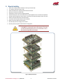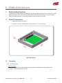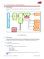
1
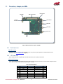
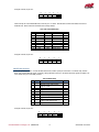
GPS18185HR Novatel GPS Carrier module User’s Manual BDM-610020094 Rev. B RTD Embedded Technologies, Inc. AS9100 and ISO 9001 Certified RTD Embedded Technologies, Inc. 103 Innovation Boulevard State College, PA 16803 USA Telephone: 814-234-8087 Fax: 814-234-5218 www.rtd.com [email protected] [email protected] Revision History Rev A Rev B 1/13/2012 Initial Release Added Software Section Added Tables 14 and 15 Advanced Analog I/O, Advanced Digital I/O, aAIO, aDIO, a2DIO, Autonomous SmartCal, “Catch the Express”, cpuModule, dspFramework, dspModule, expressMate, ExpressPlatform, HiDANplus, “MIL Value for COTS prices”, multiPort, PlatformBus, and PC/104EZ are trademarks, and “Accessing the Analog World”, dataModule, IDAN, HiDAN, RTD, and the RTD logo are registered trademarks of RTD Embedded Technologies, Inc (formerly Real Time Devices, Inc.). PS/2 is a trademark of International Business Machines Inc. PCI, PCI Express, and PCIe are trademarks of PCI-SIG. PC/104, PC/104-Plus, PCI-104, PCIe/104, PCI/104-Express and 104 are trademarks of the PC/104 Embedded Consortium. All other trademarks appearing in this document are the property of their respective owners. Failure to follow the instructions found in this manual may result in damage to the product described in this manual, or other components of the system. The procedure set forth in this manual shall only be performed by persons qualified to service electronic equipment. Contents and specifications within this manual are given without warranty, and are subject to change without notice. RTD Embedded Technologies, Inc. shall not be liable for errors or omissions in this manual, or for any loss, damage, or injury in connection with the use of this manual. Copyright © 2014 by RTD Embedded Technologies, Inc. All rights reserved. RTD Embedded Technologies, Inc. | www.rtd.com iii GPS18185HR User’s Manual Table of Contents 1 2 3 4 5 6 Introduction 7 1.1 Product Overview........................................................................................................................................................................ 7 1.2 Board Features ........................................................................................................................................................................... 7 1.3 Ordering Information ................................................................................................................................................................... 7 1.4 Contact Information .................................................................................................................................................................... 8 1.4.1 Sales Support 8 1.4.2 Technical Support 8 Specifications 9 2.1 Operating Conditions .................................................................................................................................................................. 9 2.2 Electrical Characteristics ............................................................................................................................................................ 9 Board Connection 10 3.1 Board Handling Precautions ..................................................................................................................................................... 10 3.2 Physical Characteristics ............................................................................................................................................................ 10 3.3 Connectors, Jumpers, and LEDs .............................................................................................................................................. 11 3.3.1 Bus Connectors 11 CN5: PCI Connector 11 3.3.2 I/O Connectors 11 CN1 Serial I/O Connector 11 CN2 GPS Utility Connector 12 CN3 GPS USB Connector 13 CN4 GPS 10/100 Mbps Ethernet Connector 13 CN6 GPS CAN Bus Connector 14 3.3.3 Jumpers 14 JP1 and JP2: CN1 Serial Port Source 14 JP3: CN1 Serial Port Mode 14 JP4: GPS CAN Port Selection 15 JP5: CAN Bus Termination 15 JP7: GPS Software Reset 15 JP8: 1PPS to Carrier Detect Disable 15 3.3.4 LEDs 15 One Pulse Per Second LED 15 Ethernet LEDs 15 3.4 Steps for Installing .................................................................................................................................................................... 17 IDAN Connections 18 4.1 Module Handling Precautions ................................................................................................................................................... 18 4.2 Physical Characteristics ............................................................................................................................................................ 18 4.3 Connectors................................................................................................................................................................................ 18 4.3.1 Bus Connector 18 CN5: PCI Connector 18 4.4 Steps for Installing .................................................................................................................................................................... 19 Functional Description 20 5.1 Block Diagram........................................................................................................................................................................... 20 5.2 GPS Interface ........................................................................................................................................................................... 20 5.2.1 GPS Antenna 20 5.2.2 PCI Bus UARTS 20 5.2.3 DTR GPS Reset 21 Software 6.1 22 Installing the Software .............................................................................................................................................................. 22 RTD Embedded Technologies, Inc. | www.rtd.com iv GPS18185HR User’s Manual 6.2 Serial Port Configuration ........................................................................................................................................................... 22 6.3 Software Programming ............................................................................................................................................................. 22 6.3.1 API Interface 22 6.3.2 COM Port Numbering 22 6.3.3 Base Address and Register Mapping 22 7 Troubleshooting 23 8 Additional Information 24 9 8.1 PC/104 Specifications ............................................................................................................................................................... 24 8.2 PCI and PCI Express Specification .......................................................................................................................................... 24 Limited Warranty RTD Embedded Technologies, Inc. | www.rtd.com 25 v GPS18185HR User’s Manual Table of Figures Figure 1: Board Dimensions ................................................................................................................................................................................... 10 Figure 2: Board Connections, Jumpers, and LEDs ................................................................................................................................................ 11 Figure 3: Example 104™Stack ............................................................................................................................................................................... 17 Figure 4: IDAN Dimensions .................................................................................................................................................................................... 18 Figure 5: Example IDAN System ............................................................................................................................................................................ 19 Figure 6: GPS18185 Block Diagram....................................................................................................................................................................... 20 Table of Tables Table 1: Ordering Options ........................................................................................................................................................................................ 7 Table 2: Operating Conditions .................................................................................................................................................................................. 9 Table 3: Electrical Characteristics ............................................................................................................................................................................ 9 Table 4 CN1 in RS-232 Mode................................................................................................................................................................................. 11 Table 5 CN1 in RS-422/485 Mode.......................................................................................................................................................................... 12 Table 6 CN2 GPS Utility ......................................................................................................................................................................................... 12 Table 7 CN3 GPS USB ........................................................................................................................................................................................... 13 Table 8 CN4 GPS Ethernet .................................................................................................................................................................................... 13 Table 9 CN6 GPS CAN .......................................................................................................................................................................................... 14 Table 10: JP1 and JP2 Settings ............................................................................................................................................................................. 14 Table 11: JP3 Settings ............................................................................................................................................................................................ 15 Table 12: JP4 Settings ............................................................................................................................................................................................ 15 Table 13: JP5 Settings ............................................................................................................................................................................................ 15 Table 14: JP7 Settings ............................................................................................................................................................................................ 15 Table 15: JP8 Settings ............................................................................................................................................................................................ 15 RTD Embedded Technologies, Inc. | www.rtd.com vi GPS18185HR User’s Manual 1 Introduction 1.1 Product Overview The GPS18185 is designed to provide a PCI UART interface to a Novatel OEM628 GPS. It uses a PCI/104 interface to the CPU module, and provides the ability to communicate with all three GPS serial interfaces. Additionally, the module provides connectors for Ethernet, CAN, and USB to the module. It is compatible with all PCI/104 modules. 1.2 Board Features 1.3 PCI Interface to CPU Quad UART interface to Novatel GPS modules Ethernet connector to GPS module USB connector to GPS module CAN connector to GPS module External serial interface to GPS module, optionally an RS-232/422 serial port PCI Bus: o 32-bit, 33 MHz PCI Bus o PCI Target Controller allows PCI access to quad UART Ordering Information The GPS18185 is available with the following options: Table 1: Ordering Options Part Number GPS18185HR GPS18185HR-xxx IDAN-GPS18185HRS IDAN-GPS18185HRS-xxx Description Novatel GPS Carrier Module GPS18185HR with Novatel OEM628-xxx GPS Novatel GPS Carrier Module in IDAN enclosure GPS18185HR with Novatel OEM628-xxx GPS in IDAN enclosure The Intelligent Data Acquisition Node (IDAN™) building block can be used in just about any combination with other IDAN building blocks to create a simple but rugged 104™ stack. This module can also be incorporated in a custom-built RTD HiDAN™ or HiDANplus High Reliability Intelligent Data Acquisition Node. Contact RTD sales for more information on our high reliability systems. RTD Embedded Technologies, Inc. | www.rtd.com 7 GPS18185HR User’s Manual 1.4 Contact Information 1.4.1 SALES SUPPORT For sales inquiries, you can contact RTD Embedded Technologies sales via the following methods: Phone: E-Mail: 1.4.2 1-814-234-8087 [email protected] Monday through Friday, 8:00am to 5:00pm (EST). TECHNICAL SUPPORT If you are having problems with you system, please try the steps in the Troubleshooting section of this manual. For help with this product, or any other product made by RTD, you can contact RTD Embedded Technologies technical support via the following methods: Phone: E-Mail: 1-814-234-8087 Monday through Friday, 8:00am to 5:00pm (EST). [email protected] RTD Embedded Technologies, Inc. | www.rtd.com 8 GPS18185HR User’s Manual 2 Specifications 2.1 Operating Conditions Table 2: Operating Conditions 2.2 Symbol Vcc5 Ta Ts RH Parameter 5V Supply Voltage Operating Temperature Storage Temperature Relative Humidity MTBF Mean Time Before Failure Test Condition Min 4.75 -40 -55 0 Non-Condensing Telcordia Issue 2 30°C, Ground benign, controlled Max 5.25 +85 +125 90% TBD Unit V C C % Hours Electrical Characteristics Table 3: Electrical Characteristics Symbol P Parameter Power Consumption Icc5 5V Input Supply Current VIH3.3 VIL3.3 VIH5 VIL5 IIL IOZ VOH3.3 VOL3.3 VOH5 VOL5 PCI 3.3V Input High Voltage PCI 3.3V Input Low Voltage PCI 5V Input High Voltage PCI 5V Input Low Voltage PCI Input Leakage PCI Hi-Z Leakage PCI 3.3V Output High Voltage PCI 3.3V Output Low Voltage PCI 5V Output High Voltage PCI 5V Output Low Voltage Test Condition Vcc5 = 5.0V (Without Module) Active (Without Module) PCI Bus JP300 = 1-2 (3.3V) JP300 = 1-2 (3.3V) JP300 = 2-3 (5V) JP300 = 2-3 (5V) 0<VI<VIO 0<VI<VIO JP300 = 1-2 (3.3V), IOUT = -0.5mA JP300 = 1-2 (3.3V) , IOUT = 1.5mA JP300 = 2-3 (5V) , IOUT = -12mA JP300 = 2-3 (5V) , IOUT = 12mA CAN Port Positive-going Input Threshold Negative-going Input Threshold Hysteresis Voltage Input Resistance CAN-H Output Voltage (Dominant) CAN-L CAN-H Output Voltage (Recessive) CAN-L Differential Output (Dominant) Differential Output (Recessive) Termination Resistor RTD Embedded Technologies, Inc. | www.rtd.com Min Typical 0.5 Unit W 100 1.65 0 2.0 0 -10 mA 3.3 0.7 5.5 0.8 10 10 2.97 0.33 2.4 0.4 500 20 2.75 0.5 2 2 1.2 -120 750 650 100 3.5 2.5 2.5 2 121 9 Max 900 50 4.5 2 3 3 3 12 V V V V uA uA V V V V mV mV mV KΩ V V V mV Ω GPS18185HR User’s Manual 3 Board Connection 3.1 Board Handling Precautions To prevent damage due to Electrostatic Discharge (ESD), keep your board in its antistatic bag until you are ready to install it into your system. When removing it from the bag, hold the board at the edges, and do not touch the components or connectors. Handle the board in an antistatic environment, and use a grounded workbench for testing and handling of your hardware. 3.2 Physical Characteristics Weight: Approximately 55 g (0.12 lbs.) Dimensions: 90.17 mm L x 95.89 mm W (3.550 in L x 3.775 in W) Figure 1: Board Dimensions RTD Embedded Technologies, Inc. | www.rtd.com 10 GPS18185HR User’s Manual 3.3 Connectors, Jumpers, and LEDs CN5: PCI Connector CN6: CAN Ethernet LEDs JP5: CAN Termination CN4: Ethernet CN3: USB CN2: Utility CN1: Serial SW1 Figure 2: Board Connections, Jumpers, and LEDs 3.3.1 BUS CONNECTORS CN5: PCI Connector The PCI connector is the connection to PCI peripheral modules. The position and pin assignments are compliant with the PCI/104 Specification. (See PC/104 Specifications on page 24) 3.3.2 I/O CONNECTORS All I/O connectors have Pin 1 designated by a thick white silkscreen line, and a square pad on the PCB. CN1 Serial I/O Connector CN1 is an RS-232/RS-422/RS-485 interface that can be configured to be a serial port off the CPU or one of the first two serial ports from the GPS. Table 4 is the pin out in RS-232 mode, if JP3 has pins 1 – 2 shorted. Table 4 CN1 in RS-232 Mode Pin 1 2 3 4 5 6 7 8 9, 10 UART Connection DCD DSR RxD RTS TxD CTS DTR GND RTD Embedded Technologies, Inc. | www.rtd.com GPS Connection RxD RTS TxD CTS GND 11 Function Data Carrier Detect Data Set Ready Receive Data Request To Send Transmit Data Clear To Send Data Terminal Ready Reserved Signal Ground In/Out In In In Out Out In Out GPS18185HR User’s Manual Facing the connector, the pin out is: 9 GND GND 10 7 DTR Rsvd 8 5 TxD CTS 6 3 RxD RTS 4 1 DCD DSR 2 Table 5 is the pin out of CN1 in RS422/485 mode, if JP3 has pins 2 – 3 shorted. Note that when connected to the UART, RTS is used to enable the driver. When connected to the GPS the driver is always enabled. Table 5 CN1 in RS-422/485 Mode Pin 1 2 3 4 5 6 7 8 9, 10 UART Signal RxDTxD+ TxDRxD+ GND GPS Signal RxDTxD+ TxDRxD+ GND Function Reserved Reserved Receive Data(-) Transmit Data (+) Transmit Data(-) Receive Data (+) Reserved Reserved Signal Ground In/Out In Out Out In - Facing the connector, the pin out is: 9 GND GND 10 7 Rvsd Rvsd 8 5 TxDRxD+ 6 3 RxDTxD+ 4 1 Rvsd Rvsd 2 CN2 GPS Utility Connector CN2 is the GPS Utility connector. It contains the GPS external reset, a buffered 1 pulse-per-second with a 7 ns maximum delay, the GPS Event 1 input, and three GPS LED signals. All signals go through the EPLD so they are 5 volt tolerant and the LED signals are capable of +8/4 mA. Table 6 is the pin out of the Utility connector. Table 6 CN2 GPS Utility Pin 1 Signal Reset 2 PValid 3 4 5 6 7 8 1PPS GND VARF GND Event1 GND 9 Error 10 GND Function Pull low to reset GPS Buffered Position Valid from GPS High if fix is valid Buffered 1 Pulse-per-Second from GPS Signal Ground Buffered VARF from GPS Signal Ground GPS Event1 Signal Signal Ground Buffered Error from GPS, goes high if GPS module detects an error Signal Ground In/Out In Out Out Out In Out - Facing the connector, the pin out is: 9 Error GND 10 RTD Embedded Technologies, Inc. | www.rtd.com 7 Event1 GND 8 5 VARF GND 6 12 3 1PPS GND 4 1 Reset PValid 2 GPS18185HR User’s Manual CN3 GPS USB Connector CN3 is the GPS USB port. It connects directly to the GPS USB port. Table 6 is the pin out of the USB connector. Table 7 CN3 GPS USB Pin 1 2 3 4 5 6 7 8 9 10 Signal Rsvd Rsvd USB+ Rsvd USBRsvd GND GND GND GND Function Reserved Reserved USB data (+) Reserved USB data (-) Reserved Signal Ground Signal Ground Signal Ground Signal Ground In/Out Bidirectional Bidirectional - Facing the connector, the pin out is: 9 GND GND 10 7 GND GND 8 5 USB-Dp Rsvd 6 3 USB-Dn Rsvd 4 1 Rsvd Rsvd 2 CN4 GPS 10/100 Mbps Ethernet Connector CN4 is the GPS 10/100 Mbps Ethernet port. The GPS18185 provides the magnetics required to connect the GPS directly to 10/100 Mbps network. It is full duplex with auto-negotiation enabled. Table 8 is the pin out of the Ethernet connector. Table 8 CN4 GPS Ethernet Pin 1 2 3 4 5 6 7 8 9 10 Signal RX+ RXTerm Term TX+ TXTerm Term AGND AGND Function Receive+ ReceiveEthernet Termination Ethernet Termination Transmit+ TransmitEthernet Termination Ethernet Termination Ethernet Ground Ethernet Ground Facing the connector, the pin out is: 9 AGND AGND 10 RTD Embedded Technologies, Inc. | www.rtd.com 7 Term Term 8 5 TX+ TX6 13 3 Term Term 4 1 RX+ RX2 GPS18185HR User’s Manual CN6 GPS CAN Bus Connector CN6 is the GPS CAN Bus port. The GPS18185 provides the CAN transceiver required to connect the GPS directly to CAN network. This requires the GPS module to configure COM3 as CAN. Jumper JP4 controls the GPS to CAN transceiver connection. If JP4 has pins 1 – 2 shorted GPS COM3 is connected to the UART channel 3. If JP4 has pins 2 – 3 shorted GPS COM3 is connected to the CAN transceiver. Table 9 is the pin out of the Ethernet connector. Table 9 CN6 GPS CAN Pin 1 2 3 4 5 6 7 Signal Rsvd GND CAN-L CAN-H GND Rsvd Rsvd 8 +5V* 9 10 GND Rsvd Function Reserved Signal Ground CAN bus data low CAN bus data high Signal Ground Reserved Reserved *Provides +5 volts if B1 is shorted. Default is B1 open. Signal Ground Reserved Facing the connector, the pin out is: 9 GND Rsvd 10 3.3.3 7 Rsvd +5V* 8 5 GND Rsvd 6 3 CAN-L CAN_H 4 1 Rsvd GND 2 JUMPERS On all jumpers, pin 1 is designated by a thick white silkscreen line, and a square pad on the PCB. JP1 and JP2: CN1 Serial Port Source JP1 and JP2 are 3-pin two position jumpers that are used to select if the UART or a GPS serial port is connected to CN1. These jumpers affect UART serial ports 1, 2, and 4 as well as GPS serial ports 1 and 2. Table 10 has JP1 and JP2 setting information. Table 10: JP1 and JP2 Settings JP1 Setting JP2 Setting 1–2 Any Position 1–2 2–3 2–3 Description GPS serial port 1 connected to UART serial port 1 GPS serial port 2 connected to UART serial port 2 GPS serial port 3 connected to UART serial port 3 UART serial port 4 is connected to CN1 GPS serial port 1 connected to CN1 UART serial port 1 monitors GPS serial port 1 GPS serial port 2 connected to UART serial port 2 GPS serial port 3 connected to UART serial port 3 UART serial port 4 is unused GPS serial port 1 connected to UART serial port 1 GPS serial port 2 connected to CN1 UART serial port 2 monitors GPS serial port 2 GPS serial port 3 connected to UART serial port 3 UART serial port 4 is unused Notes Factory default is 1 – 2 for both JP1 and JP2 JP3: CN1 Serial Port Mode JP3 is used to select the mode of serial port CN1. The options are shown in Table 11. RTD Embedded Technologies, Inc. | www.rtd.com 14 GPS18185HR User’s Manual Table 11: JP3 Settings Setting 1–2 2–3 Description RS-232 RS-422/485 Notes Factory default Note that in RS-422 mode when connected to the UART (JP1 is 1 – 2) RTS is used to enable the driver. When connected to the GPS (JP1 is 2 – 3) the driver is always enabled. JP4: GPS CAN Port Selection JP4 is used to select which GPS CAN port is connected to CAN transceiver and connector CN6. The options are shown in Table 12. Table 12: JP4 Settings Setting 1–2 2–3 Description GPS CAN port 1 connected to CN6 GPS CAN port 2 connected to CN6 Notes Factory default JP5: CAN Bus Termination JP5 is used terminate the CAN bus. If this device is not at the end of the CAN bus, remove this jumper. The options are shown in Table 13: JP5 Settings. Table 13: JP5 Settings Setting 1 – 2 Short 1 – 2 Open Description CAN Bus Terminated CAN Bus Not Terminated Notes Factory default JP7: GPS Software Reset JP7 is used enable/disable the DTR GPS reset. The options are shown in Table 14. Table 14: JP7 Settings Setting 1–2 2–3 Description DTR GPS Reset is Disabled DTR GPS Reset is Enabled Notes Factory default JP8: 1PPS to Carrier Detect Disable JP8 is used enable/disable the 1PPS to Carrier Detect. The options are shown in Table 14. Table 15: JP8 Settings Setting 1–2 2–3 Description 1PPS to Carrier Detect is Disabled 1PPS to Carrier Detect is Enabled Notes Factory default 3.3.4 LEDS One Pulse Per Second LED The One Pulse Per Second (1PPS) LED is connected to the 1PPS of the GPS module. The falling edge of the GPS 1PPS causes the LED to turn on for 0.5 seconds. Ethernet LEDs These two LEDs are driven by buffered GPS LED_A and LED_B signals. RTD Embedded Technologies, Inc. | www.rtd.com 15 GPS18185HR User’s Manual GPS LED_A signal goes to the green LED labeled “L” and is Link/Act. It will be on when there is an Ethernet link and flash when there is Ethernet activity. GPS LED_B signal goes to the amber LED labeled “S” and is the 100/10Mb LED. It will be on when the connection is at 100Mb and off when the connection is 10Mb. RTD Embedded Technologies, Inc. | www.rtd.com 16 GPS18185HR User’s Manual 3.4 Steps for Installing 1. 2. 3. 4. 5. 6. 7. 8. 9. 10. 11. 12. Always work at an ESD protected workstation, and wear a grounded wrist-strap. Turn off power to the PC/104 system or stack. Select and install stand-offs to properly position the module on the stack. Remove the module from its anti-static bag. Check that pins of the bus connector are properly positioned. Check the stacking order; make sure all of the busses used by the peripheral cards are connected to the cpuModule. Hold the module by its edges and orient it so the bus connector pins line up with the matching connector on the stack. Gently and evenly press the module onto the PC/104 stack. If any boards are to be stacked above this module, install them. Attach any necessary cables to the PC/104 stack. Re-connect the power cord and apply power to the stack. Boot the system and verify that all of the hardware is working properly. NOTE: When using under Windows, the GPS may be incorrectly detected as a Serial Mouse, causing erratic mouse cursor behavior. This issue has been documented by Microsoft. For more information, refer to Microsoft Knowledge Base Article 283063. Figure 3: Example 104™Stack RTD Embedded Technologies, Inc. | www.rtd.com 17 GPS18185HR User’s Manual 4 IDAN Connections 4.1 Module Handling Precautions To prevent damage due to Electrostatic Discharge (ESD), keep your module in its antistatic bag until you are ready to install it into your system. When removing it from the bag, hold the module by the aluminum enclosure, and do not touch the components or connectors. Handle the module in an antistatic environment, and use a grounded workbench for testing and handling of your hardware. 4.2 Physical Characteristics Weight: Approximately 0.21 Kg (0.46 lbs.) Dimensions: 151.972 mm L x 129.978 mm W x 16.993 mm H (5.983 in L x 5.117 in W x 0.669 in H) Figure 4: IDAN Dimensions 4.3 Connectors 4.3.1 BUS CONNECTOR CN5: PCI Connector The PCI connector is the connection to PCI peripheral modules. The position and pin assignments are compliant with the PCI-104 Specification. (See PC/104 Specifications on page 24) RTD Embedded Technologies, Inc. | www.rtd.com 18 GPS18185HR User’s Manual 4.4 Steps for Installing 1. 2. 3. 4. 5. 6. 7. 8. 9. 10. 11. 12. Always work at an ESD protected workstation, and wear a grounded wrist-strap. Turn off power to the IDAN system. Remove the module from its anti-static bag. Check that pins of the bus connector are properly positioned. Check the stacking order; make sure all of the busses used by the peripheral cards are connected to the cpuModule. Hold the module by its edges and orient it so the bus connector pins line up with the matching connector on the stack. Gently and evenly press the module onto the IDAN system. If any boards are to be stacked above this module, install them. Finish assembling the IDAN stack by installing screws of an appropriate length. Attach any necessary cables to the IDAN system. Re-connect the power cord and apply power to the stack. Boot the system and verify that all of the hardware is working properly. Figure 5: Example IDAN System RTD Embedded Technologies, Inc. | www.rtd.com 19 GPS18185HR User’s Manual 5 Functional Description 5.1 Block Diagram The Figure below shows the functional block diagram of the GPS18185. The various parts of the block diagram are discussed in the following sections. Novatel GPS PCI Quad UART CN4: Ethernet GPS Antenna PCI Bus EPLD CN1: Serial CN2: Utility CN3: USB PPS LED CN6: CAN Link LED Speed LED Figure 6: GPS18185 Block Diagram 5.2 GPS Interface The GPS18185 is a carrier board for a Novatel GPS receiver. It provides a quad UART interface to the PCI bus that can be connected to all three serial ports of the GPS and serial connector CN1. Optionally, one of the GPS serial ports can be connected to CN1. If the GPS module has CAN bus capability, it can be connected to an onboard CAN transceiver. The GPS antenna connects directly to the GPS module. 5.2.1 GPS ANTENNA The GPS antenna connects directly to the GPS module. 5.2.2 PCI BUS UARTS The GPS18185 has four PCI bus UARTS. By default they are connected as follows: UART 1 to GPS COM1 UART 2 to GPS COM2 UART 3 to GPS COM3 UART 4 to serial port connector CN1 Jumper JP1 and JP2 selection may disable some of these ports to allow the GPS COM ports to connect to serial connector CN1. Refer to Jumpers on page 14. RTD Embedded Technologies, Inc. | www.rtd.com 20 GPS18185HR User’s Manual 5.2.3 DTR GPS RESET The DTR signal of the first UART is used to generate a GPS reset signal. A reset pulse, approximately 50µs, will be generated when the DTR signal transition from asserted to de-asserted (MCR bit 0 transitions from 1 to 0). JP7 needs set to 2-3 to enable this function. RTD Embedded Technologies, Inc. | www.rtd.com 21 GPS18185HR User’s Manual 6 Software 6.1 Installing the Software The GPS18185 use a PCI UART which will require software and drivers for proper operation. Drivers are provided for Windows XP/7, DOS, and Linux Kernel 2.6.37 and newer. The drivers are provided on the companion CD and are also available on the RTD web site (http://www.rtd.com) for download. 6.2 Serial Port Configuration A software utility is required to configure serial port mode and termination setting. This utility along with source code for the utility is provided on the companion CD and is also available on the RTD web site (http://www.rtd.com) for download. For additional support concerning the software utility please contact RTD tech support. 6.3 Software Programming 6.3.1 API INTERFACE Once the drivers for the GPS18185 have been properly loaded, all four RS-232/422/485 ports should be available as standard serial ports. All four ports can then be controlled using the standard serial port interfaces built into the operating system. A description of serial port programming for operating systems is beyond the scope of this manual. Consult the operating system documentation for information on how to interface with serial ports via software. 6.3.2 COM PORT NUMBERING Serial ports (aka COM ports) are typically assigned numbers by the operating system (e.g. COM1). These numbers are typically dynamically assigned by the operating system. However, different applications may enumerate the COM ports differently, assigning different port numbers (e.g. COM3-6 vs COM5-8). When developing your own serial port application, consult your operating system’s documentation for the proper method of enumerating COM ports. Note: 6.3.3 Some applications are written to assume that no more than four COM ports are present in a system. These applications may have compatibility issues with the Exar PCI UART. BASE ADDRESS AND REGISTER MAPPING The GPS18185 exposes all of the registers available on the Exar XR17D154. The register set of the XR17D154 mimics the standard 16C550 UART register map. However, the XR17D154 contains some additional registers not found in a typical ISA-based UART. Additionally, the base address of the GPS18185’s serial ports will be different than the standard PC serial port locations (0x3F8, 0x2F8, etc). The GPS18185 is a memory mapped device. Since it is PCI-based, it may be mapped to any location within the 4GB address space of the CPU. The base address of PCI devices is determined by the CPU’s BIOS and operating system at boot time. The register-level differences between the GPS18185 and a standard 16C550 UART should be abstracted via the software drivers. Most users will not need to concern themselves with the actual registers of the board. If one is interested in directly accessing the registers of the board, consult the XR17D154 data sheet available from Exar. RTD Embedded Technologies, Inc. | www.rtd.com 22 GPS18185HR User’s Manual 7 Troubleshooting If you are having problems with your system, please try the following initial steps: Simplify the System – Remove modules one at a time from your system to see if there is a specific module that is causing a problem. Perform you troubleshooting with the least number of modules in the system possible. Swap Components – Try replacing parts in the system one at a time with similar parts to determine if a part is faulty or if a type of part is configured incorrectly. If problems persist, or you have questions about configuring this product, contact RTD Embedded Technologies via the following methods: Phone: E-Mail: +1-814-234-8087 [email protected] Be sure to check the RTD web site (http://www.rtd.com) frequently for product updates, including newer versions of the board manual and application software. RTD Embedded Technologies, Inc. | www.rtd.com 23 GPS18185HR User’s Manual 8 Additional Information 8.1 PC/104 Specifications A copy of the latest PC/104 specifications can be found on the webpage for the PC/104 Embedded Consortium: www.pc104.org 8.2 PCI and PCI Express Specification A copy of the latest PCI and PCI Express specifications can be found on the webpage for the PCI Special Interest Group: www.pcisig.com RTD Embedded Technologies, Inc. | www.rtd.com 24 GPS18185HR User’s Manual 9 Limited Warranty RTD Embedded Technologies, Inc. warrants the hardware and software products it manufactures and produces to be free from defects in materials and workmanship for one year following the date of shipment from RTD Embedded Technologies, Inc. This warranty is limited to the original purchaser of product and is not transferable. During the one year warranty period, RTD Embedded Technologies will repair or replace, at its option, any defective products or parts at no additional charge, provided that the product is returned, shipping prepaid, to RTD Embedded Technologies. All replaced parts and products become the property of RTD Embedded Technologies. Before returning any product for repair, customers are required to contact the factory for a Return Material Authorization (RMA) number. This limited warranty does not extend to any products which have been damaged as a result of accident, misuse, abuse (such as: use of incorrect input voltages, improper or insufficient ventilation, failure to follow the operating instructions that are provided by RTD Embedded Technologies, “acts of God” or other contingencies beyond the control of RTD Embedded Technologies), or as a result of service or modification by anyone other than RTD Embedded Technologies. Except as expressly set forth above, no other warranties are expressed or implied, including, but not limited to, any implied warranties of merchantability and fitness for a particular purpose, and RTD Embedded Technologies expressly disclaims all warranties not stated herein. All implied warranties, including implied warranties for merchantability and fitness for a particular purpose, are limited to the duration of this warranty. In the event the product is not free from defects as warranted above, the purchaser's sole remedy shall be repair or replacement as provided above. Under no circumstances will RTD Embedded Technologies be liable to the purchaser or any user for any damages, including any incidental or consequential damages, expenses, lost profits, lost savings, or other damages arising out of the use or inability to use the product. Some states do not allow the exclusion or limitation of incidental or consequential damages for consumer products, and some states do not allow limitations on how long an implied warranty lasts, so the above limitations or exclusions may not apply to you. This warranty gives you specific legal rights, and you may also have other rights which vary from state to state. RTD Embedded Technologies, Inc. | www.rtd.com 25 GPS18185HR User’s Manual RTD Embedded Technologies, Inc. 103 Innovation Boulevard State College, PA 16803 USA Telephone: 814-234-8087 Fax: 814-234-5218 www.rtd.com [email protected] [email protected] Copyright 2014 by RTD Embedded Technologies, Inc. All rights reserved.