1
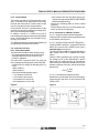
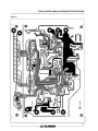
TDA9103 USER’S MANUAL DEMONSTRATION BOARD I - INTRODUCTION This demonstationboard has beenrealized in order to provide the user with a complete and simple evaluation tool of the deflection processor for multisync monitor TDA9103 (and possibly of the vertical booster TDA8172). This demoboard is in fact the core of a monitor chassis. To have a complete monitor, we have only to add a command board (microprocessor + keyboard), a line power board (EHT, S-correction, deflection transistor), a SMPS board and a video board. Besides the TDA9103 described in a separate data sheet, we will find on this board the following functions : - A vertical deflection circuit based on the TDA8172 - A class A power amplifier for the EW correction - A line transistor driver stage - A DC/DC converter for the scanning supply (so called B+) - A separable analog command board with potentiometers for the generation (from an external 5V power supply) of the 11 control voltages required by the TDA9103 and with a simulator of horizontal flyback In this way, the user will be able in a first step to evaluate the performances of the IC under clean conditions. In a second step, after having broken the printed board, he will be able to connect the demoboard to a monitor and to use the commands of an existing monitor and thus use his own software to drive the TDA9103. II - TECHNICAL INFORMATIONS II.1 - Board Description II.1.1 - Main Board II.1.1.1 - Core The board is built around the IC TDA9103 and very few external components : - C2-R32 Line oscillator. - C3-C7-R31 Filter of the line PLL. - C4 Vertical oscillator. - C5 Memory capacitor for the vertical AGC. - C26-R68-R67 Gain of the error amplifier of DC/DC converter. April 1995 - D4-R80-C48 Circuit for improvement behaviour with Composite Sync (See Section II.1.1.8. These components may be omitted if such standards are not used). II.1.1.2 - 0/5V to 2/6V Interface The IC TDA9103 uses two 8V internal voltage references VREF (for the vertical part) and HREF (for the horizontal one). So, the analog voltage range is 2 to 6V. As a microprocessor usually delivers a voltage in the range 0-5V, we must implement an interface with 3 resistors for each of the 10 adjustments required by the TDA9103 (R1 to R30). The four circuits for horizontal (resp vertical) adjustments are connected to HREF (resp VREF). II.1.1.3 - EW Amplifier The parabola generated by the TDA9103 for the EW correction must be amplified in order to drive the diode modulator. This function is performed by the class A amplifier Q3-Q4-Q9. A DC voltage is added to the parabola to achieve the horizontal size adjustments. For a proper working, this amplifier must be loaded (100Ω connected to Vp = 24V). II.1.1.4 - Horizontal Line Driver Stage The HOUT pulse delivered by the TDA9103 is used to turn on a MOS transistor via a push pull stage. The pulse is transmitted to the line transistor by a driver transformer. When Q2 is ON (HOUT at high level), the line transistor is off. You will find in annexe the specification of the transformer used on this board. Two key points of the spec must be highlighted : - Leakage inductor ≤2µH (this data set the turnoff time of the power transistor). - Parasitic capacitor < 50pf (a too high value leads to a transmission of a commutation spike to the secondary side and the chassisground and could make some trouble in the working of the chassis). 1/10 TDA9103 USER’S MANUAL DEMONSTRATION BOARD This transformer is made with a EI core from TDK (ref. PC30 EI22/19/6-Z) whose specifications are given in annexe. For a proper working, this stage is to be loaded by the following circuit (Figure 1). Figure 1 BYW98-100 BUH715 47Ω II.1.1.5 - Vertical Deflection Stage This is the typical application of the TDA8172 used with a symetrical power supply ±12V in order to avoid using a high value electrolytic capacitor. This stage is designed for driving a yoke with the following characteristics : - L ≈ 5mH - R ≈ 8Ω II.1.1.6 - B+ Converter The B+ is generated by a boost step up converter working in current mode. The power MOS Q6 starts to conduct at the beginning of the line sawtooth and it stops when the voltage on R61 (image of drain current of the MOS) becomes greater than the output voltage of the error amplifier (inside the TDA9103). This voltage is set by the regulation loop. The board offers two possibilites for choosing the regulation loop : - Local regulation of B+ : SW2 in position 1. - EHT regulation : SW2 in position 2 and feedback input on J25. This second mode will be choosen when the board is connected on a multi-frequency monitor. The main features of this converter are the following : - Frequency range 31kHz - 64kHz - Output voltage 70V - 140V - Input voltage 45V ±X% - Output power 35W max. You will find in annexe A the specifications of the inductance T2 used in this converter. 2/10 9103-62.EPS 1Ω II.1.1.7 - Other Functions X ray protection TP2 A level higher than 1.6V (TTL level) in this point inhibits all the outputs (Horizontal, Vertical, SMPS, Blanking). Blanking output TP6 This output is activated in case of Xray detection, loss of line synchro, power failure (VCC, ...) or activation of the ON/OFF switch. ON/OFF switch When the voltage on pin 2 is smaller than 1V, the HOUT, VOUT and SMPS outputs are disabled and the BLANK output TP6 is activated. CS switch J17 Theses 4 outputs are sequentially switched on (low level) if the input horizontal frequency goes through the following thresholds : 34kHz, 41kHz, 51kHz, 61kHz. These frequencies are given for a free running frequency equal to 27kHz. The CS switch outputs could be used to switch the S correction capacitors if necessary. Frame Blanking TP11 This output is in fact the flyback generator of the vertical booster TDA8172. It could be used for blanking the videosignal during the frame retrace. II.1.1.8 - Operation with Composite Sync When using these standards, the board is not driven directly by the sync signals but by a circuit (microproc or something else) who generates the Hsync and Vsync signals. Unfortunately, the Hsync signal present generally a jump of phase during the Vsync time. This phase jump disturb the line PLL and it can take a long time to recover the rightphase at the end of the vertical sync. So, we have to inhibit the line PLLduring the vertical return time (and a little later). This is done by the diode D4 and the time constant R80-C48. When Vsync is at HIGH level, the voltage on pin 35 is high and the line PLL is inhibited. The consequence is that the board will not work with standards having an inverted polarity vertical synchro. In this case, D4 must be removed or Vsync must be inverted in order to have a correct working of the line PLL. TDA9103 USER’S MANUAL DEMONSTRATION BOARD • 24V between J24 and J20 (these power supplies are only required for SMPS, LINE DRIVER and EW amplifier testing). - Connect the following loads on all the outputs (Figure 4). - Connect Hsync and Vsync from the pattern generator on J2 and J5 respectively. II.1.2 - Control Board This board, required by the first and quick evaluation, is intended to be separated from the main board for the connection to a monitor when we will use the command from the microprocessor. On this board, we find 11 potentiometers for the generation of the control voltages in the range 0-5V (use of an external power supply). In addition, thanks to a small circuit with a monostablegenerating a pseudo horizontal flyback pulse ; the demoboard can be used without connecting it to a monitor. The width and the delay of the pseudo Hflyback can be adjusted by the trimmers P1 and P2. II.2.2 - Connection to a Monitor Chassis II.2.2.1 - Analog Command and B+ Regulation Configure SW1 in position 2 and connect the board to the chassis (see Figure 5). II.2.2.2 - Analog Command and EHT Regulation Configure SW2 in position 2, connect the board as before and connect the HVFEED inputs with a shielded cable (see Figure 3). The value of R79 is suitable for getting 25kV approx high voltage value with a standard EHT transformer. When the EHV regulation loop is acting correctly, the voltage at J25 is ≈5V (depending on the B+ adjust (pin 39) voltage.It’s easy to calculate the value of R79 if the equivalent resistance Req of the bleeder is different of the one used to develop this demoboard : 5 ⋅ Req R79 ≈ EHV II.2 - Instructions for Use II.2.1 - Stand Alone Mode This demoboard is able to work alone by using : - The analog command from the control board, - A pseudo Hflyback from the control board, - A local B+ regulation. The value of B+ is preset to 100V. This value can be be changed by changing the divider R65-R66. - Configure the two jumper as following (see Figure 2) : • SW1 position 1, • SW2 position 1. - Connect the following power supply : • +12V between J3 and J19, • -12V between J21 and J19, • +5V between JC4 and JC26, • 45V 2A between J12 and J20, II.2.2.3 - Commands from Microprocessor Break off the control board and connect the appropriate outputs of the micro on the connectors J1B, J2B and J3B. Figure 2 Figure 3 SW2 R68 TP8 R26 2 R67 J25 R73 SW1 C33 FOCUS R79 75kΩ IC1 1 SW1 C35 C1 C45 SCREEN C9 S1 2 C36 TP10 C34 DEMOBOARD C2 R32 R31 EHT TRANSFORMER 9103-63.EPS R71 9103-66.EPS R72 TP9 SW2 1 3/10 4/10 9103-64.EPS The load on B+ is mandatory. Otherwise the board could be destroyed. 12kΩ 10W TDA9103 1Ω BYW98-100 5mH 8Ω 100Ω 3W 47Ω TDA9103 USER’S MANUAL DEMONSTRATION BOARD Figure 4 TDA9103 USER’S MANUAL DEMONSTRATION BOARD Figure 5 TDA9103 VSYNC HSYNC BASE DRIVE HFLY To LINE FINAL STAGE B+ GND +12V VM SMPS TRANSFORMER GND GND -12V 9103-65.EPS V YOKE To DIODE MODULATOR +24V MONITOR CHASSIS Figure 6 P2 47kΩ 14 RC C2 100pF 15 CX 12 +T Q 10 IC1b 14528 11 -T R 13 6 Q +12V P1 47kΩ Q 9 +5V 7 IC1a 14528 RC CX 2 1 C1 100pF P3 P4 P5 47kΩ 47kΩ 47kΩ Q P6 47kΩ P7 P8 P9 47kΩ 47kΩ 47kΩ P10 P11 47kΩ 47kΩ P13 47kΩ + R 3 +T -T 4 5 + C5 100nF CON1 VSIZE FHMIN SCOR VSHIFT HSHIFT HFLY 1 2 3 4 J1 1 J4 C4 10µF 1 J26 +12V C3 10µF BPLUS HOUT P12 47kΩ HDF PINCSH CCOR 9103-67.EPS +12V HSIZE KEYST 1 2 3 4 J2 1 2 3 4 5 6 7 J3 5/10 TDA9103 USER’S MANUAL DEMONSTRATION BOARD 9103-60.TIF Figure 8 7/10 TDA9103 USER’S MANUAL DEMONSTRATION BOARD 9103-60.TIF Figure 8 7/10 TDA9103 USER’S MANUAL DEMONSTRATION BOARD 9103-61.EPS TDA9103 Figure 9 8/10 TDA9103 USER’S MANUAL DEMONSTRATION BOARD III - GUIDELINES FOR LAYOUT AND WIRING SGS-THOMSON realized a demonstration board for TDA9103 scanning processor. Since this demonstration board is expected to work properly while connected to an existing monitor set with flying wires, special attention must be paid to the possible misfunctions that may be caused by the wiring. As the precautions we took may be very useful also in normal layouting, we listed them herebelow, together with other pieces of advice. III.1 - General Statement on Ground Connection The ground connectionto TDA9103 not only carries the supply current, but is also the voltage reference for various functions. Consequently, it should not carry high currents with fast transients, like : - Vertical scanning supply - Supply for B+ converter Which would introduce parasitic series voltages (resistive and inductive). This was made easier by completely separating the power sources for vertical and B+. Inside a chassis, this would necessitate separated ground pins in the SMPS transformer for ±12V (Vertical) and 45..60V (B+). III.2 - Vertical Section III.2.1 - Booster Part The +12V and -12V supplies feed the booster in first ; this way, since the ground point was kept separated, the high currents implied in vertical scanning will keep localised between the supplies and the booster. Other traditionalprecautions for the booster include : - Film capacitors C31 and C32 with low HF impedance, near to the booster with short tracks (an alternate solution is to connect C32 between pins 2 and 4) ; - ”Boucherot cell” R41, C19, near to the booster with short tracks ; - The ground track to driver stage (TDA9103) is connected to the foot of R40. III.2.2 - TDA9103 Oscillator and Driver Stage The vertical section has a dedicated reference voltage (pin 26) which should be filtered versus vertical ground (pin 24). Pin 24 may be tied to pin 19 (General ground). All elements relative to Vertical should be refered to Vertical ground (C4, C5, C40, C41, C42, C43). The oscillator capacitor C4 claims for special attention. The vertical sawtooth is obtained by charging it at low rate, then discharging abruptly. The switching from ”discharge” to ”charge” is triggered when reaching a low threshold. The loop constituted by C4 and its connecting tracks may give rise to parasitic series voltage spikes if there is a switching circuit at short distance (like the DC/DC converter for B+) ; one such spike could randomly trigger early switching to ”charge”, and the effect would be a vertical vibration of the display. Such vibrations usually occur for determined settings of the horizontal phase.To avoid this, the loop including C4 must have minimal area, and all switching circuits (SMPS, DC/DC converter, horizontal scanning) should be kept remote. III.3 - Horizontal Section III.3.1 - Oscillator Stage Like Vertical section, Horizontal section has dedicated voltage reference (pin 5) and Ground (pin 4). In order to maintain the horizontaljitter to the lowest possible value, pin 4 should be kept NOT CONNECTED TO ANY OTHER GROUND (an internal connectionalready exists with pins 19 and 24), and pin 5 should be filtered versus pin 4. This mainly concerns pins 1, 2, 3, 5, 10, 11, 12, 14, 15, 17. Moreover, the components not relatedto horizontal should not be connected to pin 4. As for Vertical section, the capacitors with their connectingtracks should not constitute large loops, prone to catch parasitic spikes. When the various DC inputs are controlled by a PWM type DAC, the DAC filtering capacitor must not be refered to pin 4, where it would produce parasitic voltages, but to the microprocessor ground ; furthermore, since there is some ripple between these two grounds, a second filter cell is needed, with its capacitor connected to pin 4. The second filter resistors are not present on the demonstration board. III.3.2 - Output Stage Usually, the horizontal scanning stage is remote from the TDA9103 and the control signal has to be transmitted at a distance. When the signal is taken from pin 21, pin 20 should be connected to GND, but not necessarily to pin 19 or near to the IC. In the typical application implemented on present board, the gate capacitance of Q2 will be charged and discharged at quite high current for every fast transition of pin 21. The current path is as follows : - For Charge : +12V (the filtering capacitor) > Q10 > R44 > gate of Q2 > source of Q2 > minus of filtering capacitor - For Discharge : gate of Q2 > Q1 > source of Q2 9/10 TDA9103 USER’S MANUAL DEMONSTRATION BOARD If these loops have too great area, they will send disturbing spikes to other circuitry by mutual inductance. For that reason the best place for transistors Q1 and Q10 is : near to the horizontal scanning transistor. This, of course, could not be implemented on present board, which does not incorporate the scanning stage. The driver stage supply voltage, present on C20, must be well filtered, since a ripple at this point will induce variations of the power transistor desaturation time, which will cause jitter. When the TDA9103 is controlled OFF, for instance by X-ray protection, Q2 will remain conductive, which causes high dissipation in R47. This may be solved if AC coupling is used between pin 21 and driver stage Q1-Q10. This was not implemented on present board. III.4 - DC/DC Converter Section III.4.1 - Keeping the Information Clean The converter section receives two informations from other parts of the chassis : - A determined fraction of the voltage to be regulated, which it will manage to keep equal to its internal reference (5V), - The voltage on the sense resistor R61, which is always lower than 1.2V. The internal references for comparison are connected to the local ground (pin 19) ; consequently, any voltage difference in the ground track could influence the regulated voltage and the peak current in Q6. To avoid this : - The foot of the divider, R79 + C47, must be grounded near to the IC (pin 19) ; if this voltage comes from a transformer,it is better to carry the information to the IC with two dedicated tracks, - The ground track between R61 and IC must carry low-value or DC currents, as explained in the first paragraph. III.4.2 - Avoiding Disturbing Spikes When Q6 switches from ON to OFF, the path of the current changes abruptly from Q6-R61 to D3-C25, and this may give rise to parasitic voltages, by mutual inductance, in all surrounding circuits (please refer to the comments about C4 in Vertical section). This effect will be minimized if both paths Q6-R61 and D3-C25 are very near to each other ; in other terms, if the loop Q6-R61-C25-R3 has a small area. The driver stage for Q6 is similar to the one for Q2 and the high surge currents in its gate may cause parasitic spikes in the same way. III.5 - Pincushion (E/W) Section All the comments relative to DAC control of the horizontal DC inputs also apply to the E/W section. Information furnished is believed to be accurate and reliable. However, SGS-THOMSON Microelectronics assumes no responsibility for the consequences of use of such information nor for any infringement of patents or other rights of third parties which may result from its use. No licence is granted by implication or otherwise under any patent or patent rights of SGS-THOMSON Microelectronics. Specifications mentioned in this publication are subject to change without notice. This publication supersedes and replaces all information previously supplied. SGS-THOMSON Microelectronics products are not authorized for use as critical components in life support devices or systems without express written approval of SGS-THOMSON Microelectronics. 1995 SGS-THOMSON Microelectronics - All Rights Reserved Purchase of I2C Components of SGS-THOMSON Microelectronics, conveys a license under the Philips I2C Patent. Rights to use these components in a I2C system, is granted provided that the system conforms to the I2C Standard Specifications as defined by Philips. SGS-THOMSON Microelectronics GROUP OF COMPANIES Australia - Brazil - China - France - Germany - Hong Kong - Italy - Japan - Korea - Malaysia - Malta - Morocco The Netherlands - Singapore - Spain - Sweden - Switzerland - Taiwan - Thailand - United Kingdom - U.S.A. 10/10