1
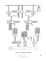
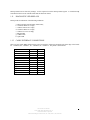
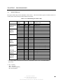
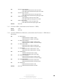
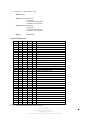
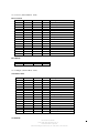
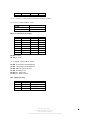
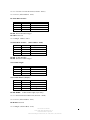
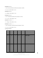
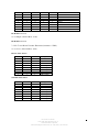
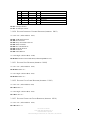
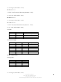
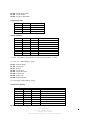
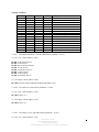
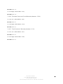
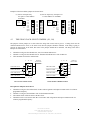
VME-SIO4A
User Manual
Manual Revision: B
General Standards Corporation
8302A Whitesburg Drive
Huntsville, AL 35802
Phone: (256) 880-8787
Fax: (256) 880-8788
URL :http://www.generalstandards.com
E-mail: [email protected]
Revision B User Manual
for the VME-SIO4: Board Revision: A
General Standards Corporation
8302A Whitesburg Drive Huntsville, AL 3580, Phone: (256) 880-8787
1
PREFACE
Copyright © 1997 General Standards Corp.
Additional copies of this manual or other General Standards Corporation literature may be obtained from:
General Standards Corporation
8302A Whitesburg Drive
Huntsville, Alabama 35802
Telephone: (256) 880-8787
Fax: (256) 880-8788
Company URL: www.generalstandards.com
The information in this document is subject to change without notice.
General Standards Corporation makes no warranty of any kind with regard to this material, including, but not
limited to, the implied warranties of merchantability and fitness for a particular purpose. Although extensive editing
and reviews are performed before release to ECO control, General Standards Corporation assumes no
responsibility for any errors that may exist in this document. No commitment is made to update or keep current the
information contained in this document.
General Standards Corporation does not assume any liability arising out of the application or use of any product
or circuit described herein, nor is any license conveyed under any patent right of any rights of others.
General Standards Corporation assumes no responsibility resulting from omissions or errors in this manual, or
from the use of information contained herein.
General Standards Corporation reserves the right to make any changes, without notice, to this product to improve
reliability, performance, function, or design.
All rights reserved
No parts of this document may be copied or reproduced in any form or by any means without prior written consent of
General Standards Corporation.
This user’s manual provides information on the specifications, theory of operation, register level programming, and
installation of the VME-SIO4 board.
Information required for customized hardware/software development.
This manual assumes that the user is familiar with the VMEbus interface specification. In an effort to avoid
redundancy, this manual relies on data books, other manuals, and specifications as indicated in the related
publication section.
Revision B User Manual
for the VME-SIO4: Board Revision: A
General Standards Corporation
8302A Whitesburg Drive Huntsville, AL 3580, Phone: (256) 880-8787
2
Related Publications
The following manuals and specifications provide the necessary information for in-depth understanding of the
VMEbus and specialized parts used on this board.
EIA Standard for the RS-422-A Interface (EIA order number EIA-RS-422A)
VMEbus Specification Manual (also known as IEC 821 BUS and IEEE P10114/D1/2), for information submit
request to:
VITA10229 North Scottsdale Road, Suite B
Scottsdale, AZ 85253
Telephone: 602-951-8866
Zilog’s USC Universal Serial Controller (part number: Z16C30) User’s Manual and Databook, for information
submit request to:
Zilog, Inc.
210 East Hacienda Ave.
Campbell, CA 95008-6600
Telephone: 408-370-8000
Revision B User Manual
for the VME-SIO4: Board Revision: A
General Standards Corporation
8302A Whitesburg Drive Huntsville, AL 3580, Phone: (256) 880-8787
3
VME-SIO4 Documentation History
1)
2)
3)
4)
5)
6)
7)
8)
9)
10)
11)
12)
The Vme-SIO4 documentation was updated March 1997.
The manual was reformatted, for conformity of text, and the table of contents was corrected.
The jumper field drawings in Chapter 4 were redrawn and double checked.
April 27, 1997: Chapter 3, page 3, Section 3.1.2.1, D6 & D7 bit descriptions were corrected, instead of: 0 will
enable Rx…, it was corrected to be a 1 will enable Rx.., and instead of 1 will disable Rx.., it was corrected to be
a 0 will disable Rx…
April 27, 1997: Chapter 4, page 2, Section 4.3, added pin numbers for J11 & J14 drawing, changed pin 6, & 11
to circles, they were previously squares which represent pin 1.
August 15, 1997: merged all files into one.
September 15, 1997: corrected errors Section 4.0 and 4.1, typos.
September 29, 1997: corrected errors, Section 1.2: deleted reference to figure 1.2-1 Corrected addresses,
Sections: 3.1.6.14.2, 3.1.6.15.1, 3.1.6.15.2, 3.1.6.25.1, and 3.1.6.25.2. Temporarily inserted Figure 1.1-1 after
Section 1.2. Verified all serial control register offset addresses.
September 30, 1997: Section 3.1.5.3, moved D3..7 and D8..15 to end of list, deleted D0..7(text). Changed
heading format, created new table of contents. Section 2.3: Reworded, Section 3.1.2.1: added note about selftimed pulse, Section 3.1.4: changed reference to: is status and is not status to: is empty and is not empty. Section
3.1.5.1: added almost to bit descriptions D11and D13. Section 3.1.5.3: inserted description of vector register
encoding. Section 3.1.6: inserted reference to Zilog references, which were also inserted into related
publications. Section 3.1.6.1.1: added WO to description. Inserted block diagram (figure 1.1-1) directly after
section 1.2. Section 1.0,a., (6): added note about VME DMA controller.
October 1, 1997: Section 3.1.1.3: added self-timed note to bit D0’s description, Section 3.1.4, Section 3.1.5.1,
and Section 3.1.5.2: reworded bit descriptions to be more understandable. Section 3.1.5.3: Changed to hardware
encoded and software selectable. Section 3.1.5: reworded serial controller note. Section 3.1.6.16: changed
Receive Data Register to Status Interrupt Control (which was left out) and inserted it’s bit descriptions. Section
3.1.6.17: made Low and High both Tx and Rx.
October 21, 1997: Section 3.0, Table 3.0-1, adress offset 0x20, changed to RO.
Sept 25, 2003 cleaned up Address Jumper Tables – Corrected error where text did not match jumpers shown.
Changed Manual Revision to B.
Revision B User Manual
for the VME-SIO4: Board Revision: A
General Standards Corporation
8302A Whitesburg Drive Huntsville, AL 3580, Phone: (256) 880-8787
4
TABLE OF CONTENTS
CHAPTER 1: INTRODUCTION............................................................................................................................8
1.0
1.1
1.2
1.3
1.4
1.5
1.6
1.7
1.8
1.9
1.10
1.11
1.12
INTRODUCTION .......................................................................................................................................8
FUNCTIONAL DESCRIPTION .................................................................................................................8
BOARD IDENTIFICATION.......................................................................................................................8
BOARD CONTROL REGISTER..............................................................................................................10
BOARD STATUS REGISTER .................................................................................................................10
SYNC WORD SELECTION .....................................................................................................................10
DATA RECEPTION .................................................................................................................................10
DATA TRANSMIT ...................................................................................................................................10
LOOP-BACK TESTING ...........................................................................................................................10
ERROR DETECTION...............................................................................................................................10
INTERRUPTS ...........................................................................................................................................10
DIAGNOSTIC LED DISPLAYS...............................................................................................................11
CABLE INTERFACE CONNECTIONS...................................................................................................11
CHAPTER 2: THEORY OF OPERATION.........................................................................................................12
2.0
2.1
2.2
2.3
2.4
THE BOARD INTERFACE ......................................................................................................................12
INTERRUPTS ...........................................................................................................................................12
DESCRIPTION OF DMA .........................................................................................................................12
CABLE ......................................................................................................................................................13
TRANSMIT RECEIVE CLOCK...............................................................................................................13
CHAPTER 3: PROGRAMMING .........................................................................................................................14
3.0
REGISTER MAP.......................................................................................................................................14
3.1
REGISTER BIT MAPS .............................................................................................................................15
3.1.1
BOARD CONTROL/STATUS REGISTERS: ......................................................................................15
3.1.1.1
3.1.1.2
3.1.1.3
3.1.1.4
3.1.2
I/O CONTROL REGISTERS:.............................................................................................................15
3.1.2.1
3.1.3
3.1.4
3.1.5
Channel 0 Control Register: (same format for Channels 1..3 Control Registers) .....................................15
Channel 0 FIFO: (same format for Channels 1..3 FIFO) ................................................................16
Channel 0 FIFO Status Register: (same format for Channels 1..3 FIFO Status Registers) .............16
INTERRUPT CONTROL/STATUS REGISTERS: ..............................................................................17
3.1.5.1
3.1.5.2
3.1.5.3
3.1.5
Board ID Register:......................................................................................................................................15
Device Type Register: ................................................................................................................................15
Board Control Register:..............................................................................................................................15
Board Status Register: ................................................................................................................................15
Interrupt Control Register...........................................................................................................................17
Interrupt Status Register (Dual Purpose Bits): (ICR - Interrupt Control Register)....................................18
Interrupt Vector Register ............................................................................................................................21
SERIAL CONTROLLER REGISTERS................................................................................................21
3.1.6.1
Channel Command/Address Register (Address: 00000)................................................................................21
3.1.6.1.1 Low WO: (Offset Address: 0x00) ..........................................................................................................21
3.1.6.1.2 High WO: (Offset Address: 0x02)..........................................................................................................22
3.1.6.2
Channel Mode Register (Address: 00001) .....................................................................................................22
3.1.6.2.1 Low: (Offset Address: 0x04)..................................................................................................................23
3.1.6.2.2 High: (Offset Address: 0x06) .................................................................................................................23
3.1.6.3
Channel Command/Status Register (Address: 00010) ...................................................................................24
3.1.6.3.1 Low: (Offset Address: 0x08)..................................................................................................................24
3.1.6.3.2 High: (Offset Address: 0x0A) ................................................................................................................24
3.1.6.4
Channel Control Register (Address: 00011) ..................................................................................................25
3.1.6.4.1 Low: (Offset Address: 0x0C) .................................................................................................................25
3.1.6.4.2 High: Address: 00011 ............................................................................................................................25
3.1.6.5
Primary Reserved Register (Address: 00100) ................................................................................................25
3.1.6.5.1 Low: (Offset Address: 0x10)..................................................................................................................25
Revision B User Manual
for the VME-SIO4: Board Revision: A
General Standards Corporation
8302A Whitesburg Drive Huntsville, AL 3580, Phone: (256) 880-8787
5
3.1.6.5.2
3.1.6.6
3.1.6.6.1
3.1.6.6.2
3.1.6.7
High: (Offset Address: 0x12) .................................................................................................................25
Secondary Reserved Register (Address: 00101) ...............................................................................26
Low: (Offset Address: 0x14)..................................................................................................................26
High: (Offset Address: 0x16) .................................................................................................................26
Test Mode Data Register (Address: 00110)......................................................................................26
3.1.6.7.1 Low: (Offset Address: 0x18)......................................................................................................................26
3.1.6.7.2 High: (Offset Address: 0x1A) ................................................................................................................26
3.1.6.8
Test Mode Control Register (Address: 00111) .................................................................................26
3.1.6.8.1
3.1.6.8.2
3.1.6.9
Clock Mode Control Register (Address: 01000)...............................................................................27
3.1.6.9.1
3.1.6.9.2
3.1.6.10
Low: (Offset Address: 0x1C) .................................................................................................................26
High: (Offset Address: 0x1E).................................................................................................................27
Low: (Offset Address: 0x20)..................................................................................................................27
High: (Offset Address: 0x22) .................................................................................................................28
Hardware Configuration Register (Address: 01001) ......................................................................28
3.1.6.10.1 Low: (Offset Address: 0x24).....................................................................................................................28
3.1.6.10.2 High: (Offset Address: 0x26) ....................................................................................................................29
3.1.6.11
Interrupt Vector Register (Address: 01010) ....................................................................................30
3.1.6.11.1 Low: (Offset Address: 0x28).....................................................................................................................30
3.1.6.11.2 High: (Offset Address: 0x2A) ...................................................................................................................30
3.1.6.12
I/O Control Register (Address: 01011)............................................................................................30
3.1.6.12.1 Low: (Offset Address: 0x2C) ....................................................................................................................30
3.1.6.12.2 High: (Offset Address: 0x2E)....................................................................................................................31
3.1.6.13
interrupt Control Register (Address: 01100)...................................................................................31
3.1.6.13.1 Low: (Offset Address: 0x30).....................................................................................................................31
3.1.6.13.2 High: (Offset Address: 0x32) ....................................................................................................................32
3.1.6.14
Daisy-Chain Control Register (Address: 01101).............................................................................32
3.1.6.14.1 Low: (Offset Address: 0x34).....................................................................................................................32
3.1.6.14.2 High RW: (Offset Address: 0x36)..............................................................................................................32
3.1.6.15
Misc. Interrupt Status Register (Address: 01110)...........................................................................33
3.1.6.15.1 Low: (Offset Address: 0x38).....................................................................................................................33
3.1.6.15.2 High: (Offset Address: 0x3A) ...................................................................................................................33
3.1.6.16
status interrupt control Register (Address: 01111) .........................................................................33
3.1.6.16.1 Low: (Offset Address: 0x3C) ....................................................................................................................33
3.1.6.16.2 High: (Offset Address: 0x3E65)................................................................................................................33
3.1.6.17
Tx/Rx Data Register (Address: 1x000) ............................................................................................34
3.1.6.17.1 Low: (Offset Address: 0x40).....................................................................................................................34
3.1.6.17.2 High: (Offset Address: 0x42) ....................................................................................................................34
3.1.6.18
Receiver Mode Register (Address: 10001) ......................................................................................34
3.1.6.18.1 Low: (Offset Address: 0x44).....................................................................................................................34
3.1.6.18.2 High: (Offset Address: 0x46) ....................................................................................................................34
3.1.6.19
Receive Command Status Register (Address: 10010)......................................................................35
3.1.6.19.1 Low: (Offset Address: 0x48).....................................................................................................................35
3.1.6.19.2 High: (Offset Address: 0x4A) ...................................................................................................................35
3.1.6.20
Receive Interrupt Control Register (Address: 10011) .....................................................................36
3.1.6.20.1 Low: (Offset Address: 0x4C) ....................................................................................................................36
3.1.6.20.2 High: (Offset Address: 0x4E)....................................................................................................................36
3.1.6.21
Receive Sync Register (Address: 10100) .........................................................................................36
3.1.6.21.1 Low: (Offset Address: 0x50).....................................................................................................................36
3.1.6.21.2 High: (Offset Address: 0x52) .....................................................................................................................36
3.1.6.22
Receive Count Limit Register (Address: 10101)..............................................................................36
3.1.6.22.1 Low: (Offset Address: 0x54)......................................................................................................................36
3.1.6.22.2 High: (Offset Address: 0x56) .....................................................................................................................36
3.1.6.23
Receive Character Count Register (Address: 10110)......................................................................36
3.1.6.23.1 Low: (Offset Address: 0x58).....................................................................................................................36
3.1.6.23.2 High: (Offset Address: 0x5A) ...................................................................................................................37
3.1.6.24
Time Constant 0 Register (Address: 10111) ....................................................................................37
3.1.6.24.1 Low: (Offset Address: 0x5C) ....................................................................................................................37
3.1.6.24.2 High: (Offset Address: 0x5E)....................................................................................................................37
Revision B User Manual
for the VME-SIO4: Board Revision: A
General Standards Corporation
8302A Whitesburg Drive Huntsville, AL 3580, Phone: (256) 880-8787
6
3.1.6.25
Transmit Mode Register (Address: 11001)......................................................................................37
3.1.6.25.1 Low: (Offset Address: 0x64).....................................................................................................................37
3.1.6.25.2 High: (Offset Address: 0x66) ....................................................................................................................37
3.1.6.26
Transmit Command/Status Register (Address: 11010)....................................................................38
3.1.6.26.1 Low: (Offset Address: 0x68).....................................................................................................................38
3.1.6.26.2 High: (Offset Address: 0x6A) ...................................................................................................................38
3.1.6.27
Transmit Interrupt Control Register (Address: 11011) ...................................................................39
3.1.6.27.1 Low: (Offset Address: 0x6C) ....................................................................................................................39
3.1.6.27.2 High: (Offset Address: 0x6E)....................................................................................................................39
3.1.6.28
Transmit Sync Register (Address: 11100) .......................................................................................39
3.1.6.28.1 Low: (Offset Address: 0x70).....................................................................................................................39
3.1.6.28.2 High: (Offset Address: 0x72) ....................................................................................................................39
3.1.6.29
Transmit Count Limit Register (Address: 11101)............................................................................39
3.1.6.29.1 Low: (Offset Address: 0x74).....................................................................................................................39
3.1.6.29.2 High: (Offset Address: 0x76) ....................................................................................................................40
3.1.6.30
Transmit Character Count Register (Address: 11110) ....................................................................40
3.1.6.30.1 Low: (Offset Address: 0x78).....................................................................................................................40
3.1.6.30.2 High: (Offset Address: 0x7A) ...................................................................................................................40
3.1.6.31
Time Constant 1 Register (Address: 11111) ....................................................................................40
3.1.6.31.1 Low: (Offset Address: 0x7C) ....................................................................................................................40
3.1.6.31.2 High: (Offset Address: 0x7E)....................................................................................................................40
CHAPTER 4: HARDWARE CONFIGURATION ..............................................................................................41
4.0
4.1
4.2
4.3
4.4
THE ON-BOARD TRANSMIT/RECEIVE CLOCK ................................................................................41
IRQ LEVEL SELECT JUMPERS (J6).....................................................................................................41
BASE ADDRESS JUMPERS (J1, J4, J5) ................................................................................................41
THE ZILOG CLOCK SELECT JUMPERS (J11, J14).............................................................................42
THE CHANNEL PIN-OUT JUMPERS (J10, J12, J13, J15) ...................................................................43
Revision B User Manual
for the VME-SIO4: Board Revision: A
General Standards Corporation
8302A Whitesburg Drive Huntsville, AL 3580, Phone: (256) 880-8787
7
CHAPTER 1: INTRODUCTION
1.0
INTRODUCTION
The VME-SI04 interface card is capable of transmitting and receiving serial data, generating interrupts, and
providing loop-back testing.
This card provides the following specific functionality:
a. VMEbus Interface:
(1) 6U card (single slot. IEEE/ANSI-1014 compliant; A16/D16 support or better.
(2) VMEbus interrupter functionality.
(3) Jumper selectable configuration of the interrupt level and programmable interrupt vectors.
(4) FIFOs (32K x 8 bit) are provided for data transmit and for data receive to increase the size of the
transmit and receive buffers
(5) User interface signal connections are provided via 4 connectors on the front panel.
(6) All data transfers to/from the FIFOs will be via host CPU writes/reads, i.e., the board does not
include a VME DMA controller, hence this board cannot act as a VME bus master.
(7) The card also provides for self-test loop-back for verification of proper operation.
b. The following two modes of loop-back testing will be supported:
(1) internal loop-back testing (does not drive cable);
(2) external loop-back testing via an external loop-back test cable.
1.1
FUNCTIONAL DESCRIPTION
As shown in the functional block diagram (see Figure 1.1-1), this board includes the following:
a. VMEbus slave interface;
b. VMEbus interrupt module;
c. board control/status registers;
d. transceiver control logic;
e. LEDs for board status indication;
f. an oscillator (for synchronization of all logic on the board);
g. a cable data driver;
h. a cable data receiver (receive voltage level converter);
i. a transmit FIFO;
j. a receive FIFO.
1.2
BOARD IDENTIFICATION
Two (2) read-only registers will be provided for board identification:
a. manufacturer’s ID; and
b. board type.
These two registers will be modeled after the VXI specification.
The manufacturer’s ID register will return 0xFEAC when read, while the board type register will return 0xF4E4
when read. These two registers will give an indication of basic board response.
Revision B User Manual
for the VME-SIO4: Board Revision: A
General Standards Corporation
8302A Whitesburg Drive Huntsville, AL 3580, Phone: (256) 880-8787
8
Figure 1.1-1: Functional Block Diagram
Revision B User Manual
for the VME-SIO4: Board Revision: A
General Standards Corporation
8302A Whitesburg Drive Huntsville, AL 3580, Phone: (256) 880-8787
9
1.3
BOARD CONTROL REGISTER
The board control register will provide configuration of the board, including the self-test modes.
1.4
BOARD STATUS REGISTER
The board status register will provide status with regard to receive FIFO status and transmit FIFO status.
1.5
SYNC WORD SELECTION
The sync word selection is used to provide an interrupt upon the reception of a particular character. This character is
software programmable.
1.6
DATA RECEPTION
Data is received into the Zilog Z16C30, after which the software may retrieve the data from the Z16C30 or the main
Rx FIFOs, depending on how the Z16C30 has been initialized.
1.7
DATA TRANSMIT
Data is received into the Zilog Z16C30, after which the software may write data to the master FIFOs or to the Zilog
depending on how the Z16C30 has been initialized. At this point, the Zilog can be placed into a transmit mode.
1.8
LOOP-BACK TESTING
The card is designed with sufficient built-in loop-back testing capability in order to allow software to perform fault
isolation to the VME card level, and replacement within 30 minutes.
The following modes of loop-back testing are supported:
a. internal loop-back testing (does not drive the cable);
b. external loop-back testing via an external loop-back test cable.
1.9
ERROR DETECTION
Error detection built into the board includes the following:
a.
b.
c.
d.
1.10
parity error detection;
CRC error detection;
Rx overrun;
Tx underrun.
INTERRUPTS
Interrupts will be provided for the following conditions:
a.
b.
c.
d.
Sync word detected;
Tx FIFO empty;
Rx FIFO not empty;
Rx FIFO almost full.
Revision B User Manual
for the VME-SIO4: Board Revision: A
General Standards Corporation
8302A Whitesburg Drive Huntsville, AL 3580, Phone: (256) 880-8787
10
Interrupt status bits are cleared by writing a 1 to the respective bit in the interrupt status register. A second interrupt
from that bit will not occur until after that status bit has been cleared.
1.11
DIAGNOSTIC LED DISPLAYS
LEDs provide for indication of the following conditions:
a.
b.
c.
d.
e.
f.
g.
h.
1.12
BIT loop-back pass/fail status (FAIL LED);
Channel 0 Receiver is empty
Channel 1 Receiver is empty
Channel 2 Receiver is empty
Channel 3 receiver is empty
IRQ Pending
VME Access
Spare LED.
CABLE INTERFACE CONNECTIONS
There are four female DB25 cable interface (user I/O interface) connectors mounted at the front edge of the board:
P3 – Channel 0, P4 – Channel 1, P5 – Channel 2, P6 – Channel 3. The pinout is shown below:
Signal Name
Lower TxD/RxD +
Lower TxD/RxD Lower CTS/DCD +
Lower CTS/DCD Lower Tx/Rx CLK +
Lower Tx/Rx CLK Upper TxD/RxD Upper TxD/RxD +
Upper CTS/DCD Upper CTS/DCD +
Upper Tx/Rx CLK Upper Tx/Rx CLK +
Rev N/R
Pin 25
Pin 12
Pin 24
Pin 11
Pin 23
Pin 10
Pin 9
Pin 22
Pin 8
Pin 21
Pin 7
Pin 20
Rev A
Pin 3
Pin 16
Pin 5
Pin 18
Pin 9
Pin 22
Pin 10
Pin 23
Pin 11
Pin 24
Pin 12
Pin 25
Revision B User Manual
for the VME-SIO4: Board Revision: A
General Standards Corporation
8302A Whitesburg Drive Huntsville, AL 3580, Phone: (256) 880-8787
11
CHAPTER 2: THEORY OF OPERATION
2.0
THE BOARD INTERFACE
This board operates as an interface for two Zilog Z16C30s, giving it Quad Channel capabilities. The Zilogs are
mapped into the base address of this board and all reads and writes are PIOs. This board does not offer DMA across
the VMEbus. All references to DMA in this documentation are in reference to moving data from the external FIFOs
into the Zilogs or from the Zilogs into the receive FIFOs, by means of an “onboard only” DMA. These FIFOs
operate as additional buffering of 32 K bytes for both transmit and receive. These FIFOs are in addition to the
internal FIFOs of the Zilog; however, these FIFOs are not at the same address location. To implement the use of the
external FIFOs, the software must first initialize the Zilog to request DMA services for transmit or receive. When
the request is made, the onboard logic will either move the data from the transmit FIFO into the Zilog or from the
Zilog into the receive FIFOs depending on which request was made.
2.1
INTERRUPTS
The interrupts on this board are divided into two sections:
a. Master Board Interrupts: For use with conditions on the board, not pertaining to the Zilogs.
b. Zilog Interrupts: For use with conditions within the Zilog, not pertaining to the Board.
The interrupts for the onboard logic use the master vector register. The interrupts for the Zilog use the Zilog vector
registers. All interrupts are mapped directly to the VME and they are prioritized via “Round Robin” going from 0 to
3 and then to the master board. No two levels of interrupts will occur at the same time. The interrupt level is
selected via jumper.
2.2
DESCRIPTION OF DMA
DMA for all channels is performed in the same manner. The request is made, that is, one of the transmit or receive
DMA request signals go active from the Zilog. The onboard DMA logic will handshake with the Zilog to either
acknowledge valid data going to the Zilog or to get receive data from the Zilog. This activity will continue until the
Zilog no longer needs DMA service, or the external FIFOs can no longer comply. If the Zilog no longer wants
DMA, it will remove its request and the DMA will stop. The conditions at which the FIFOs can no longer comply
are when during a transmit request and the transmit FIFO is empty or during a receive request when a receive FIFO
is full. Channel 0 and 1 operate using the same Zilog bus, so therefore it must arbitrate between Channel 0 transmit
and receive, as well as Channel 1 transmit and receive. This arbitration takes place without any software
initialization.
If all four (4) DMA requests are active at the same time, this will handshake one word for one request and then
proceed to the next. It will start with the receive data and will acknowledge one word for the receive of Channel 0,
then one word of the receive for Channel 1, then one word for the transmit for Channel 0, then one word of the
transmit for Channel 1 and then it will start over.
This transmission of data from one point to another will only occur if the FIFO’s are in a valid state, i.e., transmit
FIFO must not be empty; otherwise the handshake will not take place with the Zilog. Then, the Zilog will not get an
acknowledge for its’ transmit request and will get no data.
The same is true for the receive FIFO. If the receive FIFO is full, the DMA will not remove data from the Zilog.
Therefore the Zilog will not get an acknowledge, and will not have any data removed from it.
Channels 2 and 3 work in the same way, but work on a different data bus. Therefore DMAs for Channels 2 and 3, to
or from the Zilog will not affect Channels 0 and 1. This means Channel 0 can run at full speed and Channel 2 can
Revision B User Manual
for the VME-SIO4: Board Revision: A
General Standards Corporation
8302A Whitesburg Drive Huntsville, AL 3580, Phone: (256) 880-8787
12
run at full speed without interfering with each other. The VME can read and write the Zilog during DMA cycles.
However, it must wait until the end of the current DMA access when the DMA finishes its current access, then the
VME will be allowed onto the Zilog bus.
When the Zilog bus is free from the VME, the DMA will restart. The same holds true for interrupts. If a VME or
interrupt access to or from the Zilog is currently taking place, and a DMA request is made, the DMA will wait until
the current access cycle has completed and the bus for the Zilog is free before it starts the DMA transfers.
2.3
CABLE
The Cable is configured as upper and lower so that one cable can be used for both transmit and receive, therefore
allowing full duplex capabilities for each channel. Each channel has a control register that can be set to transmit
upper or lower and to receive upper or lower. It is not possible to receive both but it is possible to transmit both. If
the channel control register is not told to transmit or receive upper and not told to transmit or receive lower, then this
board will not drive the cable, nor will it load the cable, i.e., this channel will be tri-stated.
If an external loopback test is desired to be performed without a cable, the software can set it up to do transmit,
upper or lower, and to receive the same. The effect given will be an external loopback without a cable.
2.4
TRANSMIT RECEIVE CLOCK
The transmit receive clock is controlled via a 3 x 5 jumper. If the jumper is removed, for a particular clock, it is
expected that the Zilog will produce the transmit receive clock. It cannot output a clock to the half of the cable that
it is receiving from. It can output a clock to the cable it is transmitting to. If the jumper is selected for “receive
clock”, the Zilog will get its’ clock from the cable, given that the software has chosen the cable as receive. If the
Zilog clock is chosen for the onboard transmit receive clock, then the Zilog will get its’ clock from the local
oscillator, factory installed at 20.0 megahertz.
NOTE: Care must be taken when setting these jumpers. If the jumper is installed and the Zilog drives a clock out,
then a conflict between clocks will exist.
Revision B User Manual
for the VME-SIO4: Board Revision: A
General Standards Corporation
8302A Whitesburg Drive Huntsville, AL 3580, Phone: (256) 880-8787
13
CHAPTER 3: PROGRAMMING
3.0
REGISTER MAP
The register address map for the VME-SI04 is shown below.. This board contains registers for Board Control, I/O
Control, FIFO Control, Interrupt Control and Serial Controller.
Table 3.0-1 VME-SI04 Register Address Map
Board
Control/Status
Registers
Channel
Control
Registers
FIFOs
FIFO
Status
Registers
Sync Word
Registers
Interrupt
Control/Status
Registers
Serial
Controller
Registers
Address
Offset
0x00
0x02
0x08
0x0A
0x10
0x12
0x14
0x16
0x18
0x1A
0x1C
0x1E
0x20
0x22
0x24
0x26
0x28
0x2A
0x2C
0x2E
0x30
0x32
0x34
0x200-27E
0x280-2EE
0x300-37E
0x380-3EE
Size*
D16
D16
D16
D16
D16
D16
D16
D16
D16
D16
D16
D16
D16
D16
D16
D16
D16
D16
D16
D16
D16
D16
D16
D16
D16
D16
D16
Access**
RO
RO
RW
RO
RW
RW
RW
RW
RW
RW
RW
RW
RO
RO
RO
RO
RW
RW
RW
RW
RW
RW
RW
BD
BD
BD
BD
Register Name
Board ID
Device Type
Board Control
Board Status
Channel 0 Control
Channel 1 Control
Channel 2 Control
Channel 3 Control
Channel 0 FIFO
Channel 1 FIFO
Channel 2 FIFO
Channel 3 FIFO
Channel 0 FIFO Status
Channel 1 FIFO Status
Channel 2 FIFO Status
Channel 3 FIFO Status
Channel 0 Sync Word Register
Channel 1 Sync Word Register
Channel 2 Sync Word Register
Channel 3 Sync Word Register
Interrupt Control
Interrupt Status
Interrupt Vector
Channel 0 USC Control
Channel 1 USC Control
Channel 2 USC Control
Channel 3 USC Control
* The register address offset can be selected to be in short address space (A16) or in standard address
space (A24).
** RO = read only
WO = write only
RW = read/write capability
BD = Bit Dependent
Revision B User Manual
for the VME-SIO4: Board Revision: A
General Standards Corporation
8302A Whitesburg Drive Huntsville, AL 3580, Phone: (256) 880-8787
14
3.1
REGISTER BIT MAPS
All Reserved bits should be set to 0 for future compatibility. Also, the value read from a reserved bit will be
indeterminate.
3.1.1
BOARD CONTROL/STATUS REGISTERS:
3.1.1.1 Board ID Register:
D0..D16 Reads back hex CEAC
3.1.1.2 Device Type Register:
D0..D16 Reads back hex F4E4
3.1.1.3 Board Control Register:
D0
D1
D2..3
D4
D5..6
D7
D8..D15
Board Reset L (pulsed)
1 will generate a self-timed pulse that will reset the board.
(There is no need for the software to return to clear this bit)
0 will not generate a self-timed pulse that will reset the board
(There is no need for the software to return to clear this bit)
Enable Interrupts
1 will enable this board to generate VME interrupts.
0 will disable the board from generating VME interrupts.
Reserved
Spare LED On (A software controlled bit.)
1 will turn off the Fail LED
0 will turn on the Fail LED
Reserved
Fail LED On L (A software controlled bit.)
1 will turn off the Fail LED
0 will turn on the Fail LED.
Reserved
3.1.1.4 Board Status Register:
D0..D15
3.1.2
Reserved
I/O CONTROL REGISTERS:
3.1.2.1 Channel 0 Control Register: (same format for Channels 1..3 Control Registers)
D0
D1
D2
D3
Reset Tx Buffer (pulsed)
1 will generate a self-timed pulse that will reset the Tx Buffer.
(There is no need for the software to return to clear this bit)
Reset Rx Buffer (pulsed)
1 will generate a self-timed pulse that will reset the Rx Buffer.
(There is no need for the software to return to clear this bit)
Enable interrupts for channel number.
1 will enable this board to generate interrupts for this channel number.
0 will disable the board from generating interrupts for this channel number.
Reserved
Revision B User Manual
for the VME-SIO4: Board Revision: A
General Standards Corporation
8302A Whitesburg Drive Huntsville, AL 3580, Phone: (256) 880-8787
15
D4
D5
D6
D7
D8..D15
3.1.3
CHANNEL 0 FIFO: (SAME FORMAT FOR CHANNELS 1..3 FIFO)
D0..D7
D8..D15
3.1.4
En Drive Lower Cable H
1 will enable this board to drive the lower cable.
0 will disable this board from driving the lower cable.
En Drive Upper Cable H
1 will enable this board to drive the upper cable.
0 will disable this board from driving the upper cable.
En Rx Lower Cable L
1 will enable RX to drive the lower cable.
0 will disable RX from driving the lower cable.
En Rx Upper Cable L
1 will enable Rx to drive the upper cable.
0 will disable Rx from driving the upper cable.
Reserved
Valid
Reserved
CHANNEL 0 FIFO STATUS REGISTER: (SAME FORMAT FOR CHANNELS 1..3 FIFO STATUS
REGISTERS)
D0
D1
D2
D3
D4
D5
D6
D7
D8..D15
Tx FIFO Empty L
0 indicates that the Tx FIFO is empty.
1 indicates that the Tx FIFO is not empty.
Tx FIFO Almost Empty L
0 indicates that the Tx FIFO is almost empty.
1 indicates that the Tx FIFO is not almost empty.
Tx FIFO Almost Full L
0 indicates that the Tx FIFO is almost full.
1 indicates that the Tx FIFO is not almost full.
Tx FIFO Full L
0 indicates that the Tx FIFO Full L is full.
1 indicates that the Tx FIFO Full L is not full.
Rx FIFO Empty L
0 indicates that the Rx FIFO is empty.
1 indicates that the Rx FIFO is not empty.
Rx FIFO Almost Empty L
0 indicates that the Rx FIFO is almost empty.
1 indicates that the Rx FIFO is not almost empty.
Rx FIFO Almost Full L
0 indicates that the Rx FIFO is almost full.
1 indicates that the Rx FIFO is not almost full.
Rx FIFO Full L
0 indicates that the Rx FIFO is full.
1 indicates that the Rx FIFO is not full.
Reserved
Revision B User Manual
for the VME-SIO4: Board Revision: A
General Standards Corporation
8302A Whitesburg Drive Huntsville, AL 3580, Phone: (256) 880-8787
16
3.1.5
INTERRUPT CONTROL/STATUS REGISTERS:
3.1.5.1 Interrupt Control Register
D0
D1
D2
D3
D4
D5
D6
D7
D8
D9
D10
D11
D12
Enable Channel 0
Sync Detected
1 will enable this board to generate an interrupt when a sync word is detected.
0 will disable this board from generating an interrupt when a sync word is
detected.
Enable Channel 0
Tx FIFO Empty Interrupt
1 will enable this board to generate an interrupt when the Tx FIFO is empty.
0 will disable this board from generating an interrupt when the Tx FIFO is
empty.
Enable Channel 1
Sync Detected
1 will enable this board to generate an interrupt when a Sync word is detected
0 will disable this board from generating an interrupt when a Sync word is
detected.
Enable Channel 1
Tx FIFO Empty Interrupt
1 will enable this board to generate an interrupt when the Tx FIFO is empty.
0 will disable this board from generating an interrupt when the Tx FIFO is
empty.
Enable Channel 2
Tx Sync Detected
1 will enable this board to generate an interrupt when a Tx Sync word is
detected.
0 will disable this board from generating an interrupt when a Tx Sync word is
detected.
Enable Channel 2
Tx FIFO Empty Interrupt
1 will enable this board to generate an interrupt when the Tx FIFO is empty.
0 will disable this board from generating an interrupt when the Tx FIFO is
empty.
Enable Channel 3
Tx Sync Detected
1 will enable this board to generate an interrupt when a Tx Sync word is
detected.
0 will disable this board from generating an interrupt when a Tx Sync word is
detected.
Enable Channel 3
Tx FIFO Empty Interrupt
1 will enable this board to generate an interrupt when the Tx FIFO is empty.
0 will disable this board from generating an interrupt when the Tx FIFO is
empty.
Enable Channel 0
Rx FIFO Not Empty Interrupt
1 will enable this board to generate an interrupt when the Rx FIFO is not empty.
0 will disable this board from generating an interrupt when the Rx FIFO is not
empty.
Enable Channel 0
Rx FIFO Almost Full Interrupt
1 will enable this board to generate an interrupt when the Rx FIFO is full.
0 will disable this board from generating an interrupt when the Rx FIFO is full.
Enable Channel 1
Rx FIFO Not Empty Interrupt
1 will enable this board to generate an interrupt when Rx FIFO is not empty.
0 will disable this board from generating an interrupt when Rx FIFO is not
empty.
Enable Channel 1
Rx FIFO Almost Full Interrupt
1 will enable this board to generate an interrupt when the Rx FIFO is almost full.
0 will disable this board from generating an interrupt when the Rx FIFO is
almost full.
Enable Channel 2
Rx FIFO Not Empty Interrupt
Revision B User Manual
for the VME-SIO4: Board Revision: A
General Standards Corporation
8302A Whitesburg Drive Huntsville, AL 3580, Phone: (256) 880-8787
17
D13
D14
D15
1 will enable this board to generate an interrupt when the Rx FIFO is not empty.
0 will disable this board from generating an Interrupt when the Rx FIFO is not
empty.
Enable Channel 2
Rx FIFO Almost Full Interrupt
1 will enable this board to generate an interrupt when the Rx FIFO is almost full.
0 will disable this board from generating an interrupt when the Rx FIFO is
almost full.
Enable Channel 3
Rx FIFO Not Empty Interrupt
1 will enable this board to generate an interrupt when the Rx FIFO is not empty.
0 will disable this board from generating an interrupt when the Rx FIFO is not
empty.
Enable Channel 3
Rx FIFO Almost Full Interrupt
1 will enable this board to generate an interrupt when the Rx FIFO is almost full.
0 will disable this board from generating an interrupt when the Rx FIFO is
almost full.
3.1.5.2 Interrupt Status Register (Dual Purpose Bits): (ICR - Interrupt Control Register)
D0
D1
D2
D3
D4
Channel 0
Tx FIFO Sync Detected
If this interrupt is enabled:
1 indicates an interrupt has occurred.
0 indicates an interrupt has not occurred.
If this interrupt is not enabled:
0 indicates the current status of this interrupt
source.
1 being the source of the interrupt is present.
0 being not true the source of the interrupt is not present.
Channel 0
Tx FIFO Empty Interrupt
If this interrupt is enabled:
1 indicates an interrupt has occurred.
0 indicates an interrupt has not occurred.
If this interrupt is not enabled:
0 indicates the current status of this interrupt source.
1 being the source of the interrupt is present.
0 being the source of the interrupt is not present.
Channel 1
Tx FIFO Sync Detected
If this interrupt is enabled:
1 indicates an interrupt has occurred.
0 indicates an interrupt has not occurred.
If this interrupt is not enabled:
0 indicates the current status of this interrupt source.
1 being the source of the interrupt is present.
0 being the source of the interrupt is not present.
Channel 1
Tx FIFO Empty Interrupt
If this interrupt is enabled:
1 indicates an interrupt has occurred.
0 indicates an interrupt has not occurred.
If this interrupt is not enabled:
0 indicates the current status of this interrupt source.
1 being the source of the interrupt is present.
0 being the source of the interrupt is not present.
Channel 2
Sync Detected
If this interrupt is enabled:
1 indicates an interrupt has occurred.
Revision B User Manual
for the VME-SIO4: Board Revision: A
General Standards Corporation
8302A Whitesburg Drive Huntsville, AL 3580, Phone: (256) 880-8787
18
D5
D6
D7
D8
D9
D10
D11
0 indicates an interrupt has not occurred.
If this interrupt is not enabled:
0 indicates the current status of this interrupt source.
1 being the source of the interrupt is present.
0 being the source of the interrupt is not present.
Channel 2
Tx FIFO Empty Interrupt
If this interrupt is enabled:
1 indicates an interrupt has occurred.
0 indicates an interrupt has not occurred.
If this interrupt is not enabled:
0 indicates the current status of this interrupt source.
1 being the source of the interrupt is present.
0 being the source of the interrupt is not present.
Channel 3
Sync Detected
If this interrupt is enabled:
1 indicates an interrupt has occurred.
0 indicates an interrupt has not occurred.
If this interrupt is not enabled:
0 indicates the current status of this interrupt source.
1 being the source of the interrupt is present.
0 being the source of the interrupt is not present.
Channel 3
Tx FIFO Empty Interrupt
If this interrupt is enabled:
1 indicates an interrupt has occurred.
0 indicates an interrupt has not occurred.
If this interrupt is not enabled:
0 indicates the current status of this interrupt source.
1 being the source of the interrupt is present.
0 being the source of the interrupt is not present.
Channel 0
Rx FIFO Not Empty Interrupt
If this interrupt is enabled:
1 indicates an interrupt has occurred.
0 indicates an interrupt has not occurred.
If this interrupt is not enabled:
0 indicates the current status of this interrupt source.
1 being the source of the interrupt is present.
0 being the source of the interrupt is not present.
Channel 0
Rx FIFO Almost Full Interrupt
If this interrupt is enabled:
1 indicates an interrupt has occurred.
0 indicates an interrupt has not occurred.
If this interrupt is not enabled:
0 indicates the current status of this interrupt source.
1 being the source of the interrupt is present.
0 being the source of the interrupt is not present.
Channel 1
Rx FIFO Not Empty Interrupt
If this interrupt is enabled:
1 indicates an interrupt has occurred.
0 indicates an interrupt has not occurred.
If this interrupt is not enabled:
0 indicates the current status of this interrupt source.
1 being the source of the interrupt is present.
0 being the source of the interrupt is not present.
Channel 1
Rx FIFO Almost Full Interrupt
Revision B User Manual
for the VME-SIO4: Board Revision: A
General Standards Corporation
8302A Whitesburg Drive Huntsville, AL 3580, Phone: (256) 880-8787
19
D12
D13
D14
D15
If this interrupt is enabled:
1 indicates an interrupt has occurred.
0 indicates an interrupt has not occurred.
If this interrupt is not enabled:
0 indicates the current status of this interrupt source.
1 being the source of the interrupt is present.
0 being the source of the interrupt is not present.
Channel 2
Tx FIFO Not Empty Interrupt
If this interrupt is enabled:
1 indicates an interrupt has occurred.
0 indicates an interrupt has not occurred.
If this interrupt is not enabled:
0 indicates the current status of this interrupt source.
1 being the source of the interrupt is present.
0 being the source of the interrupt is not present.
Channel 2
Rx FIFO Almost Full Interrupt
If this interrupt is enabled:
1 indicates an interrupt has occurred.
0 indicates an interrupt has not occurred.
If this interrupt is not enabled:
0 indicates the current status of this interrupt source.
1 being the source of the interrupt is present.
0 being the source of the interrupt is not present.
Channel 3
Rx FIFO Not Empty Interrupt
If this interrupt is enabled:
1 indicates an interrupt has occurred.
0 indicates an interrupt has not occurred.
If this interrupt is not enabled:
0 indicates the current status of this interrupt source.
1 being the source of the interrupt is present.
0 being the source of the interrupt is not present.
Channel 3
Rx FIFO Full Interrupt
If this interrupt is enabled:
1 indicates an interrupt has occurred.
0 indicates an interrupt has not occurred.
If this interrupt is not enabled:
0 indicates the current status of this interrupt source.
1 being the source of the interrupt is present.
0 being the source of the interrupt is not present.
Revision B User Manual
for the VME-SIO4: Board Revision: A
General Standards Corporation
8302A Whitesburg Drive Huntsville, AL 3580, Phone: (256) 880-8787
20
3.1.5.3 Interrupt Vector Register
This is a hardware modifiable Interrupt Vector Register, to indicate the source of the interrupt, encoding is
as follows D0 being the LSB:
D0..D2
Hardware Encoded
000
Enable Channel 0 Sync Detected
Enable Channel 0 Tx FIFO Empty Interrupt
001
Enable Channel 1 Sync Detected
Enable Channel 1 Tx FIFO Empty Interrupt
010
Enable Channel 2 Sync Detected
Enable Channel 2 Tx FIFO Empty Interrupt
011
Enable Channel 3 Sync Detected
Enable Channel 3 Tx FIFO Empty Interrupt
100
Enable Channel 0 Rx FIFO Not Empty Interrupt
Enable Channel 0 Rx FIFO Almost Full Interrupt
101
Enable Channel 1 Rx FIFO Not Empty Interrupt
Enable Channel 1 Rx FIFO Almost Full Interrupt
110
Enable Channel 2 Rx FIFO Not Empty Interrupt
Enable Channel 2 Rx FIFO Almost Full Interrupt
111
Enable Channel 3 Rx FIFO Not Empty Interrupt
Enable Channel 3 Rx FIFO Almost Full Interrupt
D3..D7 Software Selectable
D8..D15 Reserved
3.1.5
SERIAL CONTROLLER REGISTERS
(Contact your local Zilog Represenative for Data books and User manuals in reference to the Z16C30, USC
Universal Serial Controller, for a more detailed description of the following registers, see also Related
Publications section of this document.
3.1.6.1 CHANNEL COMMAND/ADDRESS REGISTER (ADDRESS: 00000)
(same format for Channels 1..3 USC Control Registers)
3.1.6.1.1 Low WO: (Offset Address: 0x00)
D0 WO
D1..D5 WO
D6 WO
D7 WO
Upper/Lower Byte Select (Always set to Lower for
proper operation of this board)
Address 0 . .4
Byte/Word Access (Always set to Byte for proper
operation of this board)
DMA Continue
Revision B User Manual
for the VME-SIO4: Board Revision: A
General Standards Corporation
8302A Whitesburg Drive Huntsville, AL 3580, Phone: (256) 880-8787
21
3.1.6.1.2 High WO: (Offset Address: 0x02)
Mode Control
D0 WO 0 Normal Operation
1 Auto Echo
0 External Local Loop-back
1 Internal Local Loop-back
D1 WO 0 Normal Operation
0 Auto Echo
1 External Local Loop-back
1 Internal Local Loop-back
D2 WO
Channel Reset
Channel Command WO
D7
D6
D5
D4
D3
Bit Map
0
0
0
0
0
Null Command
0
0
0
0
1
Reserved
0
0
0
1
0
Reset Highest IUS
0
0
0
1
1
Reserved
0
0
1
0
0
Trigger Channel Load DMA
0
0
1
0
1
Trigger Rx DMA
0
0
1
1
0
Trigger Tx DMA
0
0
1
1
1
Trigger Rx & Tx DMA
0
1
0
0
0
Reserved
0
1
0
0
1
Rx FIFO Purge
0
1
0
1
0
Tx FIFO Purge
0
1
0
1
1
Rx & Tx FIFO Purge
0
1
1
0
0
Reserved
0
1
1
0
1
Load Rx Character Count
0
1
1
1
0
Load Tx Character Count
0
1
1
1
1
Load RX & Tx Character Count
1
0
0
0
0
Reserved
1
0
0
0
1
Load TCO
1
0
0
1
0
Load TC1
1
0
0
1
1
Load TC0 & TC1
1
0
1
0
0
Select Serial Data LSB First *
1
0
1
0
1
Select Serial Data MSB First
1
0
1
1
0
Select Straight Memory Data *
1
0
1
1
1
Select Swapped Memory Data
1
1
0
0
0
Reserved
1
1
0
0
1
Rx Purge
1
1
0
1
0
Reserved
1
1
0
1
1
Reserved
1
1
1
0
1
Reserved
1
1
1
0
1
Reserved
1
1
1
1
0
Reserved
1
1
1
1
1
Reserved
*Selected upon reset
3.1.6.2 CHANNEL MODE REGISTER (ADDRESS: 00001)
Revision B User Manual
for the VME-SIO4: Board Revision: A
General Standards Corporation
8302A Whitesburg Drive Huntsville, AL 3580, Phone: (256) 880-8787
22
3.1.6.2.1 Low: (Offset Address: 0x04)
Receiver Mode
D3 RW
0
0
0
0
0
0
0
0
1
1
1
1
1
1
1
1
D2 RW
0
0
0
0
1
1
1
1
0
0
0
0
1
1
1
1
D1 RW
0
0
1
1
0
0
1
1
0
0
1
1
0
0
1
1
D0 RW
0
1
0
1
0
1
0
1
0
1
0
1
0
1
0
1
D6 RW
2
D5 RW
1
D4 RW
0
Bit Map
Asynchronous
External Synchronous
Isochronous
Asynchronous with CV
Monosync
Bisync
HDLC
Transparent Bisync
NBIP
802.3
Reserved
Reserved
Reserved
Reserved
Reserved
Reserved
Rx Submode
D7 RW
3
3.1.6.2.2 High: (Offset Address: 0x06)
Transmitter Mode
D3 RW
0
0
0
0
0
0
0
0
1
1
1
1
1
1
1
1
D2 RW
0
0
0
0
1
1
1
1
0
0
0
0
1
1
1
1
D1 RW
0
0
1
1
0
0
1
1
0
0
1
1
0
0
1
1
D0 RW
0
1
0
1
0
1
0
1
0
1
0
1
0
1
0
1
Bit Map
Asynchronous
Reserved
Isochronous
Asynchronous with CV
Monosync
Bisync
HDLC
Transparent Bisync
NBIP
802.3
Reserved
Reserved
Slaved Monosync
Reserved
HDLC Loop
Reserved
Tx Submode
Revision B User Manual
for the VME-SIO4: Board Revision: A
General Standards Corporation
8302A Whitesburg Drive Huntsville, AL 3580, Phone: (256) 880-8787
23
D7 RW
3
D6 RW
2
D5 RW
1
D4 RW
0
3.1.6.3 CHANNEL COMMAND/STATUS REGISTER (ADDRESS: 00010)
3.1.6.3.1 Low: (Offset Address: 0x08)
Reserved
Loop Sending
On Loop
D5 RW
D6 RO
D7 RO
HDLC Tx Last Character Length
D4 RW
1
1
1
1
0
0
0
0
D3 RW
1
1
0
0
1
1
0
0
D2 RW
1
0
1
0
1
0
1
0
Bit Map
7 Bits
6 Bits
5 Bits
4 Bits
3 Bits
2 Bits
1 Bit
0 Bits
D0 RO Tx ACK
D1 RO Rx ACK
3.1.6.3.2 High: (Offset Address: 0x0A)
D2 RW Clocks Missed Latched/Unlatch
D3 RW Clocks Missed Latched/Unlatch
D4 RW DPLL in Sync/Quick Sync
D5 WO RCC FIFO Clear
D6 RO RCC FIFO Valid
D7 RO RCC FIFO Overflow
DLL Adjust/Sync Edge
D1 RW
0
0
1
1
D0 RW
0
1
1
1
Bit Map
Both Edges
Rising Edge Only
Falling Edge Only
Adjust/Sync Inhibit
Revision B User Manual
for the VME-SIO4: Board Revision: A
General Standards Corporation
8302A Whitesburg Drive Huntsville, AL 3580, Phone: (256) 880-8787
24
3.1.6.4 CHANNEL CONTROL REGISTER (ADDRESS: 00011)
3.1.6.4.1 Low: (Offset Address: 0x0C)
Rx Status Block Transfer
D7 RW
0
0
1
1
D6 RW
0
1
0
1
Bit Map
No Status Block
One Word Status Block
Two Word Status Block
Reserved
D5 RW Wait for Rx DMA Trigger
D0..4 RW Reserved
3.1.6.4.2 High: Address: 00011
Tx Status Block Transfer
D7 RW
0
0
1
1
(Offset Address: 0x0E)
D6 RW
0
1
0
1
Bit Map
No Status Block
One Word Status Block
Two Word Status Block
Reserved
D4 RW Tx Flag Preamble
D5 RW Wait for Tx DMA Trigger
Tx Preamble Length
D3 RW
0
0
1
1
D2 RW
0
1
0
1
Bit Map
8 Bits
16 Bits
32 Bits
64 Bits
Tx Preamble Pattern (All Sync)
D1 RW
0
0
1
1
D3 RW..D0 RW
D2 RW
0
1
0
1
All Zeros
All Zeros
All Ones
Alternating 1 & 0
Alternating 0 & 1
Tx Shaved Bit Length (Async Only)
3.1.6.5 PRIMARY RESERVED REGISTER (ADDRESS: 00100)
3.1.6.5.1 Low: (Offset Address: 0x10)
D0..D7 RW Reserved
3.1.6.5.2 High: (Offset Address: 0x12)
Revision B User Manual
for the VME-SIO4: Board Revision: A
General Standards Corporation
8302A Whitesburg Drive Huntsville, AL 3580, Phone: (256) 880-8787
25
D0..D7 RW Reserved
3.1.6.6 SECONDARY RESERVED REGISTER (ADDRESS: 00101)
3.1.6.6.1 Low: (Offset Address: 0x14)
D0..D7 RW Reserved
3.1.6.6.2 High: (Offset Address: 0x16)
D0..D7 RW Reserved
3.1.6.7 TEST MODE DATA REGISTER (ADDRESS: 00110)
3.1.6.7.1 Low: (Offset Address: 0x18)
D0..D7 RW Test Data 0 . .7
3.1.6.7.2 High: (Offset Address: 0x1A)
D0..D7 RW Test Data
0 . .7
3.1.6.8 TEST MODE CONTROL REGISTER (ADDRESS: 00111)
3.1.6.8.1 Low: (Offset Address: 0x1C)
Test Register Address
D4 RW
0
0
0
0
0
0
0
0
0
0
0
0
0
0
0
0
1
1
1
1
1
1
1
D3 RW
0
0
0
0
0
0
0
0
1
1
1
1
1
1
1
1
0
0
0
0
0
0
0
D2 RW
0
0
0
0
1
1
1
1
0
0
0
0
1
1
1
1
0
0
0
0
1
1
1
D1 RW
0
0
1
1
0
0
1
1
0
0
1
1
0
0
1
1
0
0
1
1
0
0
1
D0 RW
0
1
0
1
0
1
0
1
0
1
0
1
0
1
0
1
0
1
0
1
0
1
0
Bit Map
Null Address
High Byte of Shifters
CRC Byte 0
CRC Byte 1
Rx FIFO (Write)
Clock Multiplexer Outputs
CTR0 and CTR1 Counters
Clock Multiplexer Inputs
DPLL State
Low Byte of Shifters
CRC Byte 2
CRC Byte 3
Tx FIFO (Read)
Reserved
I/O and Device Status Latches
Internal Daisy Chain
Reserved
Reserved
Reserved
Reserved
Reserved
Reserved
Reserved
Revision B User Manual
for the VME-SIO4: Board Revision: A
General Standards Corporation
8302A Whitesburg Drive Huntsville, AL 3580, Phone: (256) 880-8787
26
1
1
1
1
1
1
1
1
1
0
1
1
1
1
1
1
1
1
1
0
0
0
0
1
1
1
1
1
0
0
1
1
0
0
1
1
1
0
1
0
1
0
1
0
1
Reserved
4044H
4044H
4044H
4044H
4044H
4044H
4044H
4044H
D5..D7 RW Reserved
3.1.6.8.2 High: (Offset Address: 0x1E)
D0..D7 RW Reserved
3.1.6.9 CLOCK MODE CONTROL REGISTER (ADDRESS: 01000)
3.1.6.9.1 Low: (Offset Address: 0x20)
Receive Clock Source
D2 RW
0
0
0
0
1
1
1
1
D1 RW
0
0
1
1
0
0
1
1
D0 RW
0
1
0
1
0
1
0
1
Bit Map
Disabled
/RxC Pin
/TxC Pin
DPLL Output
BRG0 Output
BRG1 Output
CTR0 Output
CTR1 Output
D3 RW
0
1
0
1
0
1
0
1
Bit Map
Disabled
/RxC Pin
/TxC Pin
DPLL Output
BRG0 Output
BRG1 Output
CTR0 Output
CTR1 Output
Transmit Clock Source
D5 RW
0
0
0
0
1
1
1
1
D4 RW
0
0
1
1
0
0
1
1
Revision B User Manual
for the VME-SIO4: Board Revision: A
General Standards Corporation
8302A Whitesburg Drive Huntsville, AL 3580, Phone: (256) 880-8787
27
DPLL Clock Source
D7 RW
0
0
1
1
D6 RW
0
1
0
1
Bit Map
BRG0 Output
BRG1 Output
/RxC Pin
/TxC Pin
3.1.6.9.2 High: (Offset Address: 0x22)
BRG0 Clock Source
D1 RW
0
0
1
1
D0 RW
0
1
0
1
Bit Map
CTR0 Output
CTR1 Output
/RxC Pin
/TxC Pin
BRG1 Clock Source
D3 RW
0
0
1
1
D2 RW
0
1
0
1
Bit Map
CTR0 Output
CTR1 Output
/RxC Pin
/TxC Pin
CRT0 Clock Source
D5 RW
0
0
1
1
D4 RW
0
1
0
1
Description
BRG0 Output
BRG1 Output
/RxC Pin
/TxC Pin
CTR1 Clock Source
D7 RW
0
0
1
1
D6 RW
0
1
0
1
Description
Disabled
Disabled
/RxC Pin
/TxC Pin
3.1.6.10 HARDWARE CONFIGURATION REGISTER (ADDRESS: 01001)
3.1.6.10.1 Low: (Offset Address: 0x24)
D1 RW BRG0 Single Cycle/Continuous
D0 RW BRG0 Enable
Rx ACK Pin Control
Revision B User Manual
for the VME-SIO4: Board Revision: A
General Standards Corporation
8302A Whitesburg Drive Huntsville, AL 3580, Phone: (256) 880-8787
28
D3 RW
0
0
1
1
D2 RW
0
1
0
1
Bit Map
3 - State Output
Rx Acknowledge Input
Output 0
Output 1
D5 RW BRG1 Enable
D4 RW BRG1 Single Cycle/Continuous
Tx ACK Pin Control
D7 RW
0
0
1
1
D6 RW
0
1
0
1
Bit Map
3 - State Output
Tx Acknowledge Input
Output 0
Output 1
3.1.6.10.2 High: (Offset Address: 0x26)
DPLL Mode
D1 RW
0
0
1
1
D0 RW
0
1
0
1
Bit Map
Disabled
NRZ/NRZI
Biphase-Mark/Space
Biphase-Level
D2 RW
0
1
0
1
Bit Map
32x Clock Mode
16x Clock Mode
8x Clock Mode
Reserved
PLL Clock Rate
RW
0
0
1
1
D5 RW
D4 RW
Accept Code Violations
CTR1 Rate Match DPLL/CTR0
CTR0 Clock Rate
D7 RW
0
0
1
1
D6 RW
0
1
0
1
Bit Map
32x Clock Mode
16x Clock Mode
8x Clock Mode
4x Clock Mode
Revision B User Manual
for the VME-SIO4: Board Revision: A
General Standards Corporation
8302A Whitesburg Drive Huntsville, AL 3580, Phone: (256) 880-8787
29
3.1.6.11 INTERRUPT VECTOR REGISTER (ADDRESS: 01010)
3.1.6.11.1 Low: (Offset Address: 0x28)
D7..D0 RW IV 0..7
3.1.6.11.2 High: (Offset Address: 0x2A)
D0 RO IV 0
Modified Vector
D3 RO
0
0
0
0
1
1
1
1
D2 RO
0
0
1
1
0
0
1
1
D1 RO
0
1
0
1
0
1
0
1
Bit Map
None
Device Status
I/O Status
Transmit Data
Transmit Status
Receive Data
Receive Status
Not Used
D4..D7 IV (4..7)
3.1.6.12 I/O CONTROL REGISTER (ADDRESS: 01011)
3.1.6.12.1 Low: (Offset Address: 0x2C)
RxC Pin Control
D2 RW
0
0
0
0
1
1
1
1
D1 RW
0
0
1
1
0
0
1
1
D0 RW
0
1
0
1
0
1
0
1
Bit Map
Input Pin
Rx Clock Output
Rx Byte Clock Output
SYNC Output
BRG0 Output
BRG1 Output
CTR0 Output
DPLL Rx Output
D4 RW
0
0
1
1
0
0
1
1
D3 RW
0
1
0
1
0
1
0
1
Bit Map
Input Pin
Tx Clock Output
Tx Byte Clock Output
Tx Complete Output
BRG0 Output
BRG1 Output
CTR1 Output
DPLL Tx Output
TxC Pin Control
D5 RW
0
0
0
0
1
1
1
1
TxD Pin Control
Revision B User Manual
for the VME-SIO4: Board Revision: A
General Standards Corporation
8302A Whitesburg Drive Huntsville, AL 3580, Phone: (256) 880-8787
30
D7 RW
0
0
1
1
D6 RW
0
1
0
1
Bit Map
Tx Data Output
3-State Output
Output 0
Output 1
3.1.6.12.2 High: (Offset Address: 0x2E)
RxREQ Pin Control
D1 RW
0
0
1
1
D0 RW
0
1
0
1
Bit Map
3-State Output
Rx Request Output
Output 0
Output 1
TxREQ Pin Control
D3 RW
0
0
1
1
D2 RW
0
1
0
1
Bit Map
3-State Output
Rx Request Output
Output 0
Output 1
D4 RW
0
1
0
1
Bit Map
/DCD Input
/DCD//SYNC Input
Output 0
Output 1
D6 RW
0
1
0
1
Bit Map
/CTS Input
/CTS Input
Output 0
Output 1
DCD Pin Control
D5 RW
0
0
1
1
CTS Pin Control
D7 RW
0
0
1
1
3.1.6.13
INTERRUPT CONTROL REGISTER (ADDRESS:
01100)
3.1.6.13.1 Low: (Offset Address: 0x30)
D0 RW Device Status IE
D1 RW I/O Status IE
D2 RW Transmit Data IE
D3 RW Transmit Status IE
D4 RW Receive Data IE
D5 RW Receive Status IE
IE Command
D7 WO
D6 WO
Bit Map
Revision B User Manual
for the VME-SIO4: Board Revision: A
General Standards Corporation
8302A Whitesburg Drive Huntsville, AL 3580, Phone: (256) 880-8787
31
0
0
1
1
0
1
0
1
Null Command
Null Command
Reset IE
Set IE
3.1.6.13.2 High: (Offset Address: 0x32)
D0 RW Reserved
VIS Level
D3 RW
0
0
0
0
1
1
1
1
D7 RW
D6 RW
D5 RW
D4 RW
D2 RW
0
0
1
1
0
0
1
1
D1 RW
0
1
0
1
0
1
0
1
Bit Map
All
All
I/O Status and Above
Transmit Data and Above
Transmit Status and Above
Receive Data and Above
Receive Status Only
None
MIE
DLC
NV
VIS
3.1.6.14 DAISY-CHAIN CONTROL REGISTER (ADDRESS: 01101)
3.1.6.14.1 Low: (Offset Address: 0x34)
D0 RW
D1 RW
D2 RW
D3 RW
D4 RW
D5 RW
Device Status IP
I/O Status IP
Transmit Data IP
Transmit Status IP
Receive Data IP
Receive Status IP
IP Command
D7 WO
0
0
1
1
D6 WO
0
1
0
1
Bit Map
Null Command
Reset IP and IUS
Reset IP
Set IP
3.1.6.14.2 High RW: (Offset Address: 0x36)
D0 RW
D1 RW
D2 RW
D3 RW
Device Status IUS
I/O Status IUS
Transmit Data IUS
Transmit Status IUS
Revision B User Manual
for the VME-SIO4: Board Revision: A
General Standards Corporation
8302A Whitesburg Drive Huntsville, AL 3580, Phone: (256) 880-8787
32
D4 RW Receive Data IUS
D5 RW Receive Status IUS
IUS Command
D7 WO
0
0
1
1
3.1.6.15
D6 WO
0
1
0
1
Bit Map
Null Command
Null Command
Reset IUS
Set IUS
MISC. INTERRUPT STATUS REGISTER (ADDRESS: 01110)
3.1.6.15.1 Low: (Offset Address: 0x38)
D0 RW
D1 RW
D2 RW
D3 RW
D4 RO
D5 RW
D6 RO
D7 RW
BRG0 ZC Latched/Unlatch
BRG1 ZC Latched/Unlatch
DPLL SYNC Latched/Unlatch
RCC Overflow Latched/Unlatch
/CTS
/CTS Latched/Unlatch
/DCD
/DCD Latched/Unlatch
3.1.6.15.2 High: (Offset Address: 0x3A)
D0 RO
D1 RW
D2 RO
D3 RW
D4 RO
D5 RW
D6 RO
D7 RW
3.1.6.16
TxREQ
/TxREQ Latched/Unlatch
/RxREQ
/RxREQ Latched/Unlatch
/TxC
/TxC Latched/Unlatch
/RxC
/RxC Latched/Unlatch
STATUS INTERRUPT CONTROL REGISTER (ADDRESS:
01111)
3.1.6.16.1 Low: (Offset Address: 0x3C)
D0 RW
D1 RW
D2 RW
D3 RW
D4 RW
D5 RW
D6 RW
D7 RW
BRG0 ZC IE
BRG1 ZC IE
DPLL SYNC IE
RCC Overflow IE
/CTS Interrupts
/CTS Interrupts
/DCD Interrupts
/DCD Interrupts
3.1.6.16.2 High: (Offset Address: 0x3E65)
D0 RW
D1 RW
D2 RW
D3 RW
/TxREQ Interrupts
TxREQ Interrupts
RxREQ Interrupts
RxREQ Interrupts
Revision B User Manual
for the VME-SIO4: Board Revision: A
General Standards Corporation
8302A Whitesburg Drive Huntsville, AL 3580, Phone: (256) 880-8787
33
D4 RW
D5 RW
D6 RW
D7 RW
TxC Interrupts
TxC Interrupts
RxC Interrupts
RxC Interrupts
3.1.6.17 TX/RX DATA REGISTER (ADDRESS: 1X000)
3.1.6.17.1 Low: (Offset Address: 0x40)
D0..7 RW - Tx/Rx Data 0..7
3.1.6.17.2 High: (Offset Address: 0x42)
D0..7 RW - Tx/Rx Data 8..15
3.1.6.18 RECEIVER MODE REGISTER (ADDRESS: 10001)
3.1.6.18.1 Low: (Offset Address: 0x44)
Rx Enable
D1 RW
0
0
1
1
D0 RW
0
1
0
1
Bit Map
Disable Immediately
Disable After Reception
Enable Without Auto-Enables
Enable With Auto-Enables
Rx Character Length
D4 RW
0
0
0
0
1
1
1
1
D3 RW
0
0
1
1
0
0
1
1
D2 RW
0
1
0
1
0
0
0
0
Bits
8
1
2
3
4
5
6
7
D5 RW Rx Parity Enable
Rx Parity Sense
D7 RW
0
0
1
1
D6 RW
0
1
0
1
Bit Map
Even
Odd
Space
Mark
3.1.6.18.2 High: (Offset Address: 0x46)
D0 RW Queue Abort
D1 RW Rx CRC Enable
Revision B User Manual
for the VME-SIO4: Board Revision: A
General Standards Corporation
8302A Whitesburg Drive Huntsville, AL 3580, Phone: (256) 880-8787
34
D2 RW Rx CRC Preset Value
Rx CRC Polynomial
D4 RW
0
0
1
1
D3 RW
0
1
0
1
Bit Map
CRC-CCITT
CRC-16
CRC-32
Reserved
Rx Data Decoding
D7 RW
0
0
0
0
1
1
1
1
D6 RW
0
0
1
1
0
0
1
1
D5 RW
0
1
0
1
0
1
0
1
Bit Map
NRZ
NRZB
NRZI-Mark
NRZI-Space
Biphase-Mark
Biphase-Space
Biphase-Level
Diff. Biphase-Level
3.1.6.19 RECEIVE COMMAND STATUS REGISTER (ADDRESS: 10010)
3.1.6.19.1 Low: (Offset Address: 0x48)
D0 RO
D1 RW
D2 RW
D3 RO
D4 RW
D5 RW
D6 RW
D7 RW
Rx Character Available
Rx Overrun
Parity Error/Frame Abort
CRC/Framing Error
Rx CV/EOT/EOF
Rx Break Abort
Rx Idle
Exited Hunt
3.1.6.19.2 High: (Offset Address: 0x4A)
D0 RO
D1 RO
D2 RO
D3 RO
Short Frame/CV Polarity
Residue Code 0
Residue code 1
Residue Code 2
Receive Command
0
0
0
0
0
0
0
0
D4 WO
0
0
0
0
1
1
1
1
D5 WO
0
0
1
1
0
0
1
1
0
1
0
1
0
1
0
1
Bit Map
Null command
Reserved
Preset CRC
Enter Hunt Mode
Reserved
Select FIFO Status
Select FIFO Interrupt Level
Select FIFO Request Level
Revision B User Manual
for the VME-SIO4: Board Revision: A
General Standards Corporation
8302A Whitesburg Drive Huntsville, AL 3580, Phone: (256) 880-8787
35
1
1
1
0
1
1
1
0
0
0
0
1
1
1
0
0
1
1
0
0
1
0
1
0
1
0
1
1
Reserved
Reserved
Reserved
Reserved
Reserved
Reserved
Reserved
D6 RO First Byte in Error
D7 RO Second Byte in Error
3.1.6.20 RECEIVE INTERRUPT CONTROL REGISTER (ADDRESS: 10011)
3.1.6.20.1 Low: (Offset Address: 0x4C)
D0 RW
D1 RW
D2 RW
D3 RW
D4 RW
D5 RW
D6 RW
D7 RW
TC0R Read Count/TC
Rx Overrun IA
Parity Error/Frame Abort IA
Status on Words
Rx CV/EOT/EOF IA
Rx Break/Abort IA
Rx Idle IA
Exited Hunt IA
3.1.6.20.2 High: (Offset Address: 0x4E)
D0..D7 RW Rx FIFO Control and Status (Fill/Interrupt/DMA Level)
3.1.6.21 RECEIVE SYNC REGISTER (ADDRESS: 10100)
3.1.6.21.1 Low: (Offset Address: 0x50)
D0..D7 RW RSYN 0..7
3.1.6.21.2 High: (Offset Address: 0x52)
D0..D7 RW RSYN 0..7
3.1.6.22 RECEIVE COUNT LIMIT REGISTER (ADDRESS: 10101)
3.1.6.22.1 Low: (Offset Address: 0x54)
D0..7 RW RCL 0..7
3.1.6.22.2 High: (Offset Address: 0x56)
D0..7 RW RCL 0..7
3.1.6.23 RECEIVE CHARACTER COUNT REGISTER (ADDRESS: 10110)
3.1.6.23.1 Low: (Offset Address: 0x58)
D0..7 RO RCC 0..7
Revision B User Manual
for the VME-SIO4: Board Revision: A
General Standards Corporation
8302A Whitesburg Drive Huntsville, AL 3580, Phone: (256) 880-8787
36
3.1.6.23.2 High: (Offset Address: 0x5A)
D0..7 RO RCC 0..7
3.1.6.24 TIME CONSTANT 0 REGISTER (ADDRESS: 10111)
3.1.6.24.1 Low: (Offset Address: 0x5C)
D0..7 RW TC0 0..7
3.1.6.24.2 High: (Offset Address: 0x5E)
D0..7 RW TC0 0..7
3.1.6.25 TRANSMIT MODE REGISTER (ADDRESS: 11001)
3.1.6.25.1 Low: (Offset Address: 0x64)
Tx Enable
D1 RW
0
0
1
1
D0 RW
0
1
0
1
Bit Map
Disable Immediately
Disable After Transmission
Enable Without Auto-Enables
Enable With Auto-Enables
Tx Character Length
D4 RW
0
0
0
0
1
1
1
1
D3 RW
0
0
1
1
0
0
1
1
D2 RW
0
1
0
1
0
1
0
1
Bit Maps
8 Bits
1 Bit
2 Bits
3 Bits
4 Bits
5 Bits
6 Bits
7 Bits
D5 RW Tx Parity Enable
Tx Parity Sense
D7 RW
0
0
1
1
D6 RW
0
1
0
1
Bit Map
Even
Odd
Space
Mark
3.1.6.25.2 High: (Offset Address: 0x66)
Revision B User Manual
for the VME-SIO4: Board Revision: A
General Standards Corporation
8302A Whitesburg Drive Huntsville, AL 3580, Phone: (256) 880-8787
37
D2 RW Tx CRC Preset Value
D1 RW Tx CRC Enable
D0 RW Tx CRC on EOF/EOM
Polynomial Tx CRC
D4 RW
0
0
1
1
D3 RW
0
1
0
1
Bit Map
CRC-CCITT
CRC-16
CRC-32
Reserved
Tx Data Encoding
D7 RW
0
0
0
0
1
1
1
1
D6 RW
0
0
1
1
0
0
1
1
D5 RW
0
1
0
1
0
1
0
1
Bit Map
NRZ
NRZB
NRZI-Mark
NRZI-Space
Biphase-Mark
Biphase-Space
Biphase-Level
Diff. Biphase-Level
3.1.6.26 TRANSMIT COMMAND/STATUS REGISTER (ADDRESS: 11010)
3.1.6.26.1 Low: (Offset Address: 0x68)
D0 RO
D1 RW
D2 RO
D3 RW
D4 RW
D5 RW
D6 RW
D7 RW
Tx Buffer Empty
Tx Underrun
All Sent
Tx CRC Sent
Tx EOF/EOT Sent
Tx Abort Sent
Tx Idle Sent
Tx Preamble Sent
3.1.6.26.2 High: (Offset Address: 0x6A)
Tx Idle Line Condition
D2 RW
D1 RW
0
0
0
0
0
1
0
1
1
0
1
0
1
1
1
1
D3 RW Tx Wait on Underrun
D0 RW
0
1
0
1
0
1
0
1
Bit Map
SYNC/Flag/Normal
Alternating 1 & 0
All Zeros
All Ones
Reserved
Alternating Mark & Space
Space
Mark
Revision B User Manual
for the VME-SIO4: Board Revision: A
General Standards Corporation
8302A Whitesburg Drive Huntsville, AL 3580, Phone: (256) 880-8787
38
Transmit Command
D7 WO
0
0
0
0
0
0
1
0
1
1
1
1
1
1
1
1
D6 WO
0
0
0
0
1
1
1
1
0
0
0
0
1
1
1
1
D5 WO
0
0
1
1
0
0
1
1
0
0
1
1
0
0
1
1
D4 WO
0
1
0
1
0
1
0
1
0
1
0
1
0
1
0
1
Bit Map
Null Command
Reserved
Preset CRC
Reserved
Reserved
Select FIFO Status
Select FIFO Interrupt Level
Select FIFO Request Level
Send Frame/Message
Send Abort
Reserved
Reserved
Reset DLE Inhibit
Set DLE Inhibit
Reset EOF/EOM
Set EOF/EOM
3.1.6.27 TRANSMIT INTERRUPT CONTROL REGISTER (ADDRESS: 11011)
3.1.6.27.1 Low: (Offset Address: 0x6C)
D0 RW
D1 RW
D2 RW
D3 RW
D4 RW
D5 RW
D6 RW
D7 RW
TC1R Read Count/TC
Tx Overrun IA
Wait for Send Command
Tx CRC Sent IA
Tx EOF/EOT Sent IA
Tx Abort Sent IA
Tx Idle Sent IA
Tx Preamble Sent IA
3.1.6.27.2 High: (Offset Address: 0x6E)
D0..7 RW Tx FIFO Control and Status (Fill/Interrupt/DMA Level)
3.1.6.28 TRANSMIT SYNC REGISTER (ADDRESS: 11100)
3.1.6.28.1 Low: (Offset Address: 0x70)
D0..7 RW TSYN 0..7
3.1.6.28.2 High: (Offset Address: 0x72)
D0..7 RW TSYN 0..7
3.1.6.29 TRANSMIT COUNT LIMIT REGISTER (ADDRESS: 11101)
3.1.6.29.1 Low: (Offset Address: 0x74)
Revision B User Manual
for the VME-SIO4: Board Revision: A
General Standards Corporation
8302A Whitesburg Drive Huntsville, AL 3580, Phone: (256) 880-8787
39
D0..7 RW TCL 0..7
3.1.6.29.2 High: (Offset Address: 0x76)
D0..7 RW TCL 0..7
3.1.6.30 TRANSMIT CHARACTER COUNT REGISTER (ADDRESS: 11110)
3.1.6.30.1 Low: (Offset Address: 0x78)
D0..7 RO TCC 0..7
3.1.6.30.2 High: (Offset Address: 0x7A)
D0..7 RO TCC 0..7
3.1.6.31 TIME CONSTANT 1 REGISTER (ADDRESS: 11111)
3.1.6.31.1 Low: (Offset Address: 0x7C)
D0..7 RW TC1 0..7
3.1.6.31.2 High: (Offset Address: 0x7E)
D0..7 RW TC1 0..7
Revision B User Manual
for the VME-SIO4: Board Revision: A
General Standards Corporation
8302A Whitesburg Drive Huntsville, AL 3580, Phone: (256) 880-8787
40
CHAPTER 4: HARDWARE CONFIGURATION
4.0
THE ON-BOARD TRANSMIT/RECEIVE CLOCK
The on-board oscillator, U28, is used for generating a transmit receive clock as well as the on-board clock for the
Zilogs. It is factory installed at 20.0 MHz and may be changed to accommodate a wide range of baud rates. The
desired baud rate is determined by the equation:
(Baud rate) (Time Constant + 1) = Oscillator frequency of U28
Using the factory installed 20.0 megahertz oscillator frequency of U28, the following time constants will give the
following baud rates:
Time
Constants
64
256
512
2048
Baud
Rates
307.2K
76.8K
38.4K
9.6K
Any standard dip oscillator, 8 pin or 14 pin, will fit into the socket of U28, thereby changing the on-board transmit
receive clock.
4.1
IRQ LEVEL SELECT JUMPERS (J6)
These jumpers are used to select or determine the interrupt request level used by this board.
They use a binary encoded method with jumpers for pins 1 and 2 being the LSB of a 3-bit value. If none of the
jumpers are in, this is a level select of the lowest priority (7). If all the jumpers are installed, this is a level select of 0
and invalid level select.
Examples of different level select configurations are as follows:
(a) Set for
Level 5
(b) Set for
Level 2
(c) Set for
Level 3
Pin 1
Pin 5
4.2
BASE ADDRESS JUMPERS (J1, J4, J5)
Base address selection involves 3 sets of jumpers. They are J1, J4, and J5. J4 is used to select A16 or A24 space and
supervisory or non-supervisory accesses. The jumper for pins 1 and 2 is not installed for address space A24 and is
installed for address space A16. Pins 3 and 4 of J4, is installed for non-supervisory; and not installed for
supervisory.
Revision B User Manual
for the VME-SIO4: Board Revision: A
General Standards Corporation
8302A Whitesburg Drive Huntsville, AL 3580, Phone: (256) 880-8787
41
Examples of the base address jumpers are shown below:
(a) Set for non-supervisory
A16 space at a base address
of 0xC000:
A10
A11
A12
A13
A14
A15
Spare
Spare
A24
Super
J4
A16
A17
A18
A19
A20
A21
A22
A23
J1
4.3
(b) Set for supervisory A24 space at a
at a base address of 0x948000.
A24
Super
J4
A10
A11
A12
A13
A14
A15
Spare
Spare
A16
A17
A18
A19
A20
A21
A22
A23
J5
J1
J5
THE ZILOG CLOCK SELECT JUMPERS (J11, J14)
The purpose of these jumpers is to select where the Zilog clock comes from or goes to. If Zilog clock uses the
onboard transmit/receive clock, or the cable clock, then the jumpers should be installed. If the Zilog is going to
generate an output clock to the cable, then some of the jumpers should not be installed. The Zilog Clock Select
Jumpers are shown below:
•
•
•
Channel 0/2 Zilog uses the onboard OSC, U28, for Transmit and Receive.
Channel 1/3 Zilog uses the onboard OSC for Transmit and cable Receive clock for Receive.
Cable Transmit clock will be onboard OSC.
1
6
11
1
On-Board
Rx/Tx Clock
Chan 0 Rx Clock
Chan 2 Rx Clock
Chan 0 Tx Clock
Chan 2 Tx Clock
Chan 1 Rx Clock
Chan 3 Rx Clock
Chan 1 Tx Clock
Chan 3 Tx Clock
5
10 15
J11 is used for Channels 0 and 1
5
6
11
On-Board
Rx/Tx Clock
10 15
J14 is used for Channels 2 and 3
Description of Jumpers shown above:
•
•
•
•
Channel 0/2 Zilog uses the on-board OSC for Rcv and will generate and output a transmit clock of a software
programmed frequency.
Channel 1/3 Zilog uses the enable Rx clock for both transmit and Rcv.
The transmit clock will be the same as the Rcv clock.
Channel 0/2 and 1/3 will use the cable Rcv clock for Rcv and will generate and output a transmit clock of a
software programmed frequency.
Revision B User Manual
for the VME-SIO4: Board Revision: A
General Standards Corporation
8302A Whitesburg Drive Huntsville, AL 3580, Phone: (256) 880-8787
42
4.4
THE CHANNEL PIN-OUT JUMPERS (J10, J12, J13, J15)
Jumpers J10, J12, J13, and J15 may be removed to allow wire wrapping to accommodate various pin-out
configurations. It is the suggestion of GSC that any reconfiguration of the pin-out should always maintain paired
signals on the cable, i.e., the “+” signals should travel beside or be twisted with the “-“ signal.
If the jumpers are installed in the factory configuration, then the following pin-outs will apply:
Table 4.4-1 Pin-Out for User Connectors (P3 Channel 0, P4 Channel 1, P5 Channel 2, P6 Channel 3)
Jumper
Pin #
1-2
3-4
5-6
7-8
9-10
11-12
13-14
15-16
17-18
19-20
21-22
23-24
25-26
27-28
29-30
31-32
33-34
35-36
37- 38
Signal Name
LWR Cable TxD/RxD +
LWR Cable TxD/RxD NC
LWR Cable Cts/DCD +
LWR Cable Cts/DCD NC
NC
Ground
Ground
NC
NC
LWR Cable Tx/Rx/CLK +
LWR Cable Tx/Rx/CLK UPR Cable TxD/RxD UPR Cable TxD/RxD +
UPR Cable CTS/DCD UPR Cable CTS/DCD +
UPR Cable Tx/Rx/CLK UPR Cable Tx/Rx/CLK +
Connector
Pin #
3
16
5
18
7
20
9
22
10
23
11
24
12
25
Revision B User Manual
for the VME-SIO4: Board Revision: A
General Standards Corporation
8302A Whitesburg Drive Huntsville, AL 3580, Phone: (256) 880-8787
43