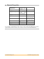
1
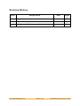
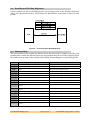
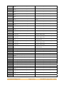
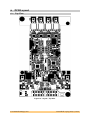
Sundance Multiprocessor Technology Limited User Manual Form : QCF42 Date : 6 July 2006 Unit / Module Description: Multi-output DDS based SLB Mezzanine Unit / Module Number: SMT399-160 Document Issue Number: 3 Issue Date: 24/05/2007 Original Author: PSR User Manual for SMT399-160 Sundance Multiprocessor Technology Ltd, Chiltern House, Waterside, Chesham, Bucks. HP5 1PS. This document is the property of Sundance and may not be copied nor communicated to a third party without prior written permission. © Sundance Multiprocessor Technology Limited 2006 User Manual SMT399-160 Last Edited: 24/05/2007 17:12:00 Revision History Issue Changes Made Date Initial s 1 Original Document 08/01/2007 PSR 2 Power consumption added 12/01/2007 PSR 3 Modification: MMBX connectors fitted 24/05/2007 SM User Manual SMT399-160 Page 2 of 39 Last Edited: 24/05/2007 17:12:00 Table of Contents 1 Introduction............................................................................................... 6 2 Related Documents .................................................................................... 7 3 Examples of application. ............................................................................ 8 4 Functional Description............................................................................... 9 4.1 Block Diagram ................................................................................................................9 4.2 Module Description ........................................................................................................9 4.3 SMT399-160 characteristics. .......................................................................................10 4.4 Power Supply structure. ...............................................................................................10 4.5 On-board crystal. ...........................................................................................................11 4.6 Output Variable Gain Amplifier....................................................................................11 4.7 Daughter sub-module interface. ...................................................................................11 4.8 Cascading modules .......................................................................................................11 4.9 Dual-tone Mode. ........................................................................................................... 12 4.10 External Trigger............................................................................................................ 12 4.11 5 LEDs.............................................................................................................................. 13 Control Register Settings...........................................................................13 5.1 Control Packet Structure .............................................................................................. 13 5.2 Reading and Writing Registers .................................................................................... 14 5.3 Memory Map................................................................................................................. 14 5.4 Register Descriptions ................................................................................................... 16 5.4.1 Reset and Update Register – 0x0............................................................................ 16 5.4.2 Profile Register – 0x1. ............................................................................................. 18 5.4.3 VGA0 Register – 0x2. .............................................................................................. 18 5.4.4 VGA1 Register – 0x3................................................................................................ 19 5.4.5 VGA2 Register – 0x4 ............................................................................................... 19 5.4.6 VGA3 Register – 0x5. .............................................................................................. 19 5.4.7 DDS0 Register – 0x6 – Control Function Register............................................... 20 5.4.8 DDS0 Register – 0x7 – Control Function Register. ...............................................22 5.4.9 DDS0 Register – 0x8 – Control Function Register................................................23 5.4.10 DDS0 Register – 0x9 – Amplitude Scale Factor. ...................................................25 5.4.11 DDS0 Register – 0xA – Amplitude Ramp Rate......................................................25 5.4.12 DDS0 Register – 0xB – Frequency Tuning Word 0...............................................25 5.4.13 DDS0 Register – 0xC – Frequency Tuning Word 0...............................................26 5.4.14 DDS0 Register – 0xD – Phase Offset Word. ..........................................................26 5.4.15 DDS0 Register – 0xE – Frequency Tuning Word 1. ..............................................26 5.4.16 DDS0 Register – 0xF – Frequency Tuning Word 1................................................27 User Manual SMT399-160 Page 3 of 39 Last Edited: 24/05/2007 17:12:00 5.4.17 DDS0 Register – 0x10 – RAM Segment Control Word 0. .....................................27 5.4.18 DDS0 Register – 0x11 – RAM Segment Control Word 0.......................................27 5.4.19 DDS0 Register – 0x12 – RAM Segment Control Word 0. .................................... 28 5.4.20 DDS0 Register – 0x13 – RAM Segment Control Word 1. ..................................... 28 5.4.21 DDS0 Register – 0x14 – RAM Segment Control Word 1. ..................................... 28 5.4.22 DDS0 Register – 0x15 – RAM Segment Control Word 1. ..................................... 28 5.4.23 DDS0 Register – 0x16 – RAM Segment Control Word 2.......................................29 5.4.24 DDS0 Register – 0x17 – RAM Segment Control Word 2.......................................29 5.4.25 DDS0 Register – 0x18 – RAM Segment Control Word 2. .....................................29 5.4.26 DDS0 Register – 0x19 – RAM Segment Control Word 3.......................................29 5.4.27 DDS0 Register – 0x1A – RAM Segment Control Word 3. .................................... 30 5.4.28 DDS0 Register – 0x1B – RAM Segment Control Word 3. .................................... 30 5.4.29 DDS0 Register – 0x1C – Falling Delta Frequency Tuning.................................... 30 5.4.30 DDS0 Register – 0x1D – Falling Delta Frequency Word....................................... 31 5.4.31 DDS0 Register – 0x1E – Falling Sweep Ramp Rate Word. ................................... 31 5.4.32 DDS0 Register – 0x1F – Rising Delta Frequency Tuning...................................... 31 5.4.33 DDS0 Register – 0x20 – Rising Delta Frequency Word........................................32 5.4.34 DDS0 Register – 0x21 – Rising Sweep Ramp Rate Word......................................32 6 PCB Layout............................................................................................... 33 6.1 Top View .......................................................................................................................33 6.2 Bottom View..................................................................................................................34 7 Connector Location .................................................................................. 35 8 Support Packages ..................................................................................... 36 9 Physical Properties .................................................................................. 37 10 Safety ....................................................................................................... 38 11 EMC ......................................................................................................... 39 User Manual SMT399-160 Page 4 of 39 Last Edited: 24/05/2007 17:12:00 Table of Figures Figure 1 - Examples of applications..............................................................................................8 Figure 2 - SMT399-160 Block Diagram. ......................................................................................9 Figure 3 - Output main characteristics. .....................................................................................10 Figure 4 - Connections for cascading modules. ..........................................................................11 Figure 5 - Multi module synchronisation connectors................................................................ 12 Figure 6 - Dual-Tone Mode. ....................................................................................................... 12 Figure 7 – Setup Packet Structure.............................................................................................. 13 Figure 8 – Control Register Read Sequence. ............................................................................. 14 Figure 9 – Register Memory Map. ............................................................................................. 16 Figure 10 - Layout - Top Side. ....................................................................................................33 Figure 11 - Layout - Bottom Side. ...............................................................................................34 Figure 12 - Connector Location. .................................................................................................35 User Manual SMT399-160 Page 5 of 39 Last Edited: 24/05/2007 17:12:00 1 Introduction The SMT399-160 is a multi-output mezzanine single width module, which is able to generate sine waves at up to 160MHz. This mezzanine board is to be fitted on one of Sundance SLB (Sundance LVDS Bus) base modules, such as SMT338-VP or SMT398-VP or SMT368 and cannot be used on its own. It is built around two AD9954s, Direct Digital Synthesizer (DDS – Analog Devices) featuring 14-bit DAC operating/sampling at up to 400 MHz. Both devices are separately programmable, can contain up to 4 profiles and have the possibility of being synchronised. The architecture allows generating single-tone or dual-tone signals. DDS outputs are split into two legs, each of them featuring a programmable amplifier (VGA). The SMT399-160 has got in total two pairs of outputs. A Xilinx FPGA Virtex-II Pro (or Virtex4) from the base module, is used to control DDSs and Variable Gain Amplifiers (VGAs) of the SMT399-160, after receiving command words via a Comport. SMT399-160 modules can be cascaded and work into the AD9954 Master/Slave mode. PCB connectors are MMBXs from Hubert Suhner. It can be used in the following application: - Radio systems, as a clock generator (fine tuning), - Test systems (dual tone and fast hopping), - Programmable system (software programmable), - Etc… User Manual SMT399-160 Page 6 of 39 Last Edited: 24/05/2007 17:12:00 2 Related Documents AD9954 Datasheet - Analog Devices: http://www.analog.com/Analog_Root/productPage/productHome/0,2121,AD9954,00.html Sundance High-speed Bus (SHB) specifications – Sundance. ftp://ftp2.sundance.com/Pub/documentation/pdf-files/SHB_Technical_Specification.pdf Sundance LVDS Bus (SLB) – Sundance. http://www.sundance.com/docs/SLB%20-%20Technical%20Specifications.pdf TIM specifications - TI. ftp://ftp2.sundance.com/Pub/documentation/pdf-files/tim_spec_v1.01.pdf Xilinx Virtex-II PRO FPGA - Xilinx. http://direct.xilinx.com/bvdocs/publications/ds083.pdf MMBX Connectors – Hubert Suhner. MMBX Connectors User Manual SMT399-160 Last Edited: 24/05/2007 17:12:00 3 Examples of application. The SMT399-160 module can be used in the following application: - Radio systems. Compatible with Sundance’s TIM Modules, it can be combined with DAQ modules such as ADCs and DACs, as a clock generator. The SMT399-160 finetuning makes it even more suitable for such platform to generate up-to-four synchronised and/or quadrature signals. - Test systems. It is sometimes very helpful to have a signal generator capable of generators various frequencies to evaluate some radio system. Fast hopping is the key word here. Dual tone signals are useful to characterise a receiver system to evaluate its capabilities of receiving signals close to each other in frequency. DDSs also to generate a ramp, a pattern or a frequency sweep. - Programmable system. As most of system, it a very important top control every part of a system. The SMT399-160 is fully controllable via software. - Etc… As both pairs of DDSs are synchronised and coupled master/slave, the module can generate 90-degree phase shift signals and be part of a quadrature modulator system. Ext. Ext. Clk ADCs Ext. Clk DAC I Clock SMT390-VP Dual 210-MSPS ADC ChA0 SMT370 Q Dual ADC/DAC Analogue Converters ChA0 Up to 160MHz Quadrature ChA1 SMT399-160 ChB0 ChB1 SMT399-160 ChB0 Up to 160MHz Quadrature Up to 160MHz Ext. ChB1 I Clock Channel A and Channel B synchronised Analogue Converters Up to 160MHz ChA1 SMT390-VP Dual 210-MSPS ADC All channels synchronised Q Ext. Clk ADCs Ext. Clk DAC SMT370 Dual ADC/DAC Analogue Converters Analogue Converters Dual Quadrature Sampling Multi-DAQ synchronisation ChA0 Up to 160MHz Ext. Clocks ChA1 Analog Inputs SMT399-160 ChB0 ChB1 Up to 160MHz or test pattern SMT390-VP Dual 210-MSPS ADC Analogue Converters Sampling with test pattern Figure 1 - Examples of applications. User Manual SMT399-160 Last Edited: 24/05/2007 17:12:00 4 Functional Description In this part, we will see the general block diagram and some comments on the main entities. 4.1 Block Diagram The following diagram shows the block diagram of the SMT399-160. 68 I/O pins +3.3V, +5V Sundance SLB base module (SMT338-VP, SMT398-VP or SMT368 for example) Syn in SMT399-160 SLB Trig A squ are A I/Os Trig B AD8370 VGA A0 AD8370 VGA A1 AD8370 VGA B0 AD8370 VGA B1 External Reference (Option) On-board Crystal 1xAD9954 DDS (Channel A) 14-bit @ 400MSPS 48-pin TQFP I/Os I/Os Synchronisation 1xAD9954 DDS (Channel B) 14-bit @ 400MSPS 48-pin TQFP I/Os Daughter Module - SMT399-160 squ are B Syn out Figure 2 - SMT399-160 Block Diagram. 4.2 Module Description The module is built around two Direct Digital Synthesizers (DDS): two AD9954. The AD9954 is a DDS featuring 14-bit DAC operating at up to 400MSPS. It forms a digitally programmable high frequency synthesizer capable of generating an analog output sinusoidal waveform at up to 160MHz. The AD9954 provides fast frequency hopping and fine-tuning resolution (32-bit frequency tuning word). The AD9954 includes an integrated 1024x32 static RAM to support flexible frequency sweep capability in several modes. It also supports a user defined linear sweep mode of operation. The frequency resolution of the AD9954 is 0.0931 Hz when clocked at 400MHz. Both analog outputs can be linked together via jumpers in order to generate a dual tone signal. User Manual SMT399-160 Last Edited: 24/05/2007 17:12:00 DDS outputs are doubled and combined with Variable Gain Amplifiers (VGA). Analog signals are all single-ended and output on MMBX connectors (J13, J14, J15 and J20) for connection to a 50-Ohm load. Output Sine waves can be turned into ‘sharp’ square signals using the AD9954 built-in comparator. Square signals (one per DDS) are also available on MMBX connectors (J24 and J25) on LVTTL format. All DDS settings travel via the FPGA present on SLB base module. Information comes from a Comport and the FPGA stores it first into internal registers and interfaces it to the DDS chips via the SLB connector. Comports follow the Texas Instrument C4x standard. 4 green LEDs are also available and driven by the FPGA to report working or failing conditions to the user. Other green LEDs show that all power supplies are ON and working. Two external triggers (J11 and J23) are also available. 4.3 SMT399-160 characteristics. Analog Outputs (J13, J14, J15 and J20). 0 to 2.12 Volts without saturation (sine wave) Analog Output Voltage Range 0 to 3.0 Volts with saturation (Output level set via Control Register - VGA) Output Impedance Frequency range Frequency resolution Terminated to be connected to a 50-Ohm load. Up to 160 MHz 0.0931 Hz Square Outputs (J24 and J25). Output Format Frequency range Frequency Resolution LVTTL Up to 160 MHz 0.0931 Hz External Triggers (J11 and J23). LVTTL (default FPGA PAD setting) Input Range Frequency Range Up to 160 MHz Input Reference (Option – J21) Frequency range 0 to 400 MHz. Figure 3 - Output main characteristics. 4.4 Power Supply structure. The SMT399-160 conforms to the TIM standard for single width modules. The TIM connectors supply 5 Volts to the base module, which also requires an additional 3.3-Volt power supply, which must be provided by the two diagonally opposite mounting holes. This 3.3-volt is present on all Sundance TIM carrier boards. From these two power rails, are generated a filtered 3.3-volt as well as a 1.8-volt source for both AD9954s. Greens LEDs placed on the board report the state of the power supplies. The SMT399-160 requires 2 power rails from the SLB power connector: +3.3 and +5 Volts. User Manual SMT399-160 Page 10 of 39 Last Edited: 24/05/2007 17:12:00 4.5 On-board crystal. The AD9954 are clocked from a crystal (20MHz). The master DDS then passes the sampling clock to the slave DDS to ensure synchronisation. Synchronisation can also be achieved when cascading several SMT399-160 daughter modules. There is an automatic synchronisation available from the DDS registers. 4.6 Output Variable Gain Amplifier. Each output is driven by a Variable Gain Amplifier (VGA – AD8370), digitally controlled that uses 8 bits to code the gain and provides a power-down mode. Two ranges of gains are available: from –11 to +17dBs or from +6 to +34dBs. 4.7 Daughter sub-module interface. The link between the main and the daughter sub-module is made via two Samtec connectors. There is no fast signal travelling between both cards. The first connector passes control signals and the second one passes a 3.3-volt and 5-volt supplies and a ground between submodules. The female differential connector is located on the main module. The Samtec Part Number for this connector is QTH-060-01-F-D-DP-A. The female power connector is located on the main module. The Samtec Part Number for this connector is BKS-133-03-F-V-A The male differential connector is located on the daughter card. The Samtec Part Number for this connector is QSH-060-01-F-D-DP-A The male power connector is located on the daughter card. The Samtec Part Number for this connector is BKT-133-03-F-V-A The mated height between the main module and the daughter card is 5 mm. 4.8 Cascading modules Several SMT399-160s can be cascaded. All DDSs can be synchronised by linking the modules via connectors J1 and J3, both are 2-mm 3-pin headers. J1 of the master module should be connected to J3 of the slave module as follows: SMT399-160 Master (J1) SMT399-160 Slave (J3) Crystal Out Crystal In (J1 – pin 1) (J3 – pin 3) Gnd Gnd (J1 – pin 2) (J3 – pin 2) Synch In Synch Out (J1 – pin 3) (J3 – pin 1) Figure 4 - Connections for cascading modules. User Manual SMT399-160 Page 11 of 39 Last Edited: 24/05/2007 17:12:00 Figure 5 - Multi module synchronisation connectors. 4.9 Dual-tone Mode. The SMT399-160 can used as a dual-tone generator. Both DDS outputs can be mixed together. In this case, all four analog outputs (J13, J14, J15 and J20) would show the same signal, at relevant amplitudes. To configure the SMT399-160 into the dual-tone mode, simply fit J16, J17, J18 and J19 in place. The normal mode of operation is obtained by leaving J16, J17, J18 and J19 open. Figure 6 - Dual-Tone Mode. 4.10 External Trigger. Two external triggers are available on J23 and J11. Both are straight through, i.e. the connector is directly connected to the FPGA. There is no protection so it is to the user to make sure levels present on the connector are compatible with the pad implemented in the FPGA. In the default firmware provided, J23 is connected to LED1 and J11 to LED3 (see silkscreen for LED locations). User Manual SMT399-160 Page 12 of 39 Last Edited: 24/05/2007 17:12:00 4.11 LEDs. There are 8 LEDs on the board. Only 4 are user defined, i.e. accessible from the FPGA on the SLB base module. These 4 leds are labelled on silkscreen LED1, LED2, LED3 and LED4. In the standard firmware provided with the board, LED0 and LED2 are flashing in opposite phase as soon as the FPGA is configured and the on-board crystal of the SLB based module is working. LED1 is connected directly to the trigger signal coming from J11. LED3 is connected directly to the trigger signal coming from J23. External triggers have no more action than driving LED1 and LED3. The other 4 LEDs are connected on power rails and should be ON at all time. If not it is strongly recommended to put the module off power and to contact Sundance. 5 Control Register Settings The Control Registers control the complete functionality of the SMT399-160. They are setup via the Comport3 in the standard FPGA firmware provided. 5.1 Control Packet Structure The data passed on to the SMT399-160 over the Comports must conform to a certain packet structure. Only valid packets will be accepted and only after acceptance of a packet will the appropriate settings be implemented. Each packet will start with a certain sequence indicating the start of the packet (0xFF). The address to write the data payload into will follow next. After the address the data will follow. This structure is illustrated in the following figure: Byte Content Byte Bit 7 Bit 6 Bit 5 Bit 4 Bit 3 Bit 2 Bit 1 Bit 0 0 ‘1’ ‘1’ ‘1’ ‘1’ ‘1’ ‘1’ ‘1’ ‘1’ 1 Address 7 Address 6 Address 5 Address 4 Address 3 Address 2 Address 1 Address 0 3 Data 15 Data 14 Data 13 Data 12 Data 11 Data 10 Data 9 Data 8 4 Data 7 Data 6 Data 5 Data 4 Data 3 Data 2 Data 1 Data 0 Figure 7 – Setup Packet Structure. User Manual SMT399-160 Page 13 of 39 Last Edited: 24/05/2007 17:12:00 5.2 Reading and Writing Registers Control packets are sent to the SMT399-160 over Comport3 only in the standard firmware. This is a bi-directional interface. The format of a ‘Read Packet’ is the same as that of a write packet. Figure 8 – Control Register Read Sequence. 5.3 Memory Map The write packets must contain the address where the data must be written to and the read packets must contain the address where the required data must be read. The following figure shows the memory map for the writable and readable Control Registers on the SMT399-160: Address Writable Registers Readable Registers 0x00 Reset and Update Register. Reserved. 0x01 DDS0 and 1 Profile Register. DDS0 and DDS1 Profile Register. 0x02 VGA0. Read-back (FPGA Register) VGA0. 0x03 VGA1. Read-back (FPGA Register) VGA1. 0x04 VGA2. Read-back (FPGA Register) VGA2. 0x05 VGA3. Read-back (FPGA Register) VGA3. 0x06 DDS0 – Register 0 (0x0) – Control Function Register. Read-back (FPGA Register) DDS0 – Register 0 (0x0). 0x07 DDS0 – Register 1 (0x1) – Control Function Register. Read-back (FPGA Register) DDS0 – Register 1 (0x1). 0x08 DDS0 – Register 2 (0x2) – Control Function Register. Read-back (FPGA Register) DDS0 – Register 2 (0x2). 0x09 DDS0 – Register 3 (0x3) – Amplitude Scale Factor Register. Read-back (FPGA Register) DDS0 – Register 3 (0x3). 0x0A DDS0 – Register 4 (0x4) – Amplitude Ramp Rate Register. Read-back (FPGA Register) DDS0 – Register 4 (0x4). 0x0B DDS0 – Register 5 (0x5) – Frequency Tuning Word 0. Read-back (FPGA Register) DDS0 – Register 5 (0x5). 0x0C DDS0 – Register 6 (0x6) – Frequency Tuning Word 0. Read-back (FPGA Register) DDS0 – Register 6 (0x6). 0x0D DDS0 – Register 7 (0x7) – Phase Offset Word. Read-back (FPGA Register) DDS0 – Register 7 (0x7). 0x0E DDS0 – Register 8 (0x8) – Frequency Tuning Word 1. Read-back (FPGA Register) DDS0 – Register 8 (0x8). 0x0F DDS0 – Register 9 (0x9) – Frequency Tuning Word 1. Read-back (FPGA Register) DDS0 – Register 9 (0x9). 0x10 DDS0 – Register A (0xA) – RAM Segment Control Word 0. Read-back (FPGA Register) DDS0 – Register A (0xA). User Manual SMT399-160 Page 14 of 39 Last Edited: 24/05/2007 17:12:00 0x11 DDS0 – Register B (0xB) – RAM Segment Control Word 0. Read-back (FPGA Register) DDS0 – Register B (0xB). 0x12 DDS0 – Register C (0xC) – RAM Segment Control Word 0. Read-back (FPGA Register) DDS0 – Register C (0xC). 0x13 DDS0 – Register D (0xD) – RAM Segment Control Word 1. Read-back (FPGA Register) DDS0 – Register D (0xD). 0x14 DDS0 – Register E (0xE) – RAM Segment Control Word 1. Read-back (FPGA Register) DDS0 – Register E (0xE). 0x15 DDS0 – Register F (0xF) – RAM Segment Control Word 1. Read-back (FPGA Register) DDS0 – Register F (0xF). 0x16 DDS0 – Register 10 (0x10) – RAM Segment Control Word 2. Read-back (FPGA Register) DDS0 – Register 10 (0x10). 0x17 DDS0 – Register 11 (0x11) – RAM Segment Control Word 2. Read-back (FPGA Register) DDS0 – Register 11 (0x11). 0x18 DDS0 – Register 12 (0x12) – RAM Segment Control Word 2. Read-back (FPGA Register) DDS0 – Register 12 (0x12). 0x19 DDS0 – Register 13 (0x13) – RAM Segment Control Word 3. Read-back (FPGA Register) DDS0 – Register 13 (0x13). 0x1A DDS0 – Register 14 (0x1A) – RAM Segment Control Word 3. Read-back (FPGA Register) DDS0 – Register 14 (0x14). 0x1B DDS0 – Register 15 (0x1B) – RAM Segment Control Word 3. Read-back (FPGA Register) DDS0 – Register 15 (0x15). 0x1C DDS0 – Register 16 (0x1C) – Falling Delta Frequency Tuning Word. Read-back (FPGA Register) DDS0 - Falling Delta Frequency Tuning Word. 0x1D DDS0 – Register 17 (0x1D) – Falling Delta Frequency Tuning Word. Read-back (FPGA Register) DDS0 - Falling Delta Frequency Tuning Word. 0x1E DDS0 – Register 18 (0x1E) – Falling Sweep Ramp rate Word. Read-back (FPGA Register) DDS0 - Falling Sweep Ramp rate Word. 0x1F DDS0 – Register 19 (0x1F) – Rising Delta Frequency Tuning Word. Read-back (FPGA Register) DDS0 - Rising Delta Frequency Tuning Word. 0x20 DDS0 – Register 20 (0x20) – Rising Delta Frequency Tuning Word. Read-back (FPGA Register) DDS0 - Rising Delta Frequency Tuning Word. 0x21 DDS0 – Register 21 (0x21) – Rising Sweep Ramp rate Word. Read-back (FPGA Register) DDS0 - Rising Sweep Ramp rate Word. 0x26 DDS1 – Register 0 (0x0) – Control Function Register. Read-back (FPGA Register) DDS1 – Register 0 (0x0). 0x27 DDS1 – Register 1 (0x1) – Control Function Register. Read-back (FPGA Register) DDS1 – Register 1 (0x1). 0x28 DDS1 – Register 2 (0x2) – Control Function Register. Read-back (FPGA Register) DDS1 – Register 2 (0x2). 0x29 DDS1 – Register 3 (0x3) – Amplitude Scale Factor Register. Read-back (FPGA Register) DDS1 – Register 3 (0x3). 0x2A DDS1 – Register 4 (0x4) – Amplitude Ramp Rate Register. Read-back (FPGA Register) DDS1 – Register 4 (0x4). 0x2B DDS1 – Register 5 (0x5) – Frequency Tuning Word 0. Read-back (FPGA Register) DDS1 – Register 5 (0x5). 0x2C DDS1 – Register 6 (0x6) – Frequency Tuning Word 0. Read-back (FPGA Register) DDS1 – Register 6 (0x6). 0x2D DDS1 – Register 7 (0x7) – Phase Offset Word. Read-back (FPGA Register) DDS1 – Register 7 (0x7). 0x2E DDS1 – Register 8 (0x8) – Frequency Tuning Word 1. Read-back (FPGA Register) DDS1 – Register 8 (0x8). 0x2F DDS1 – Register 9 (0x9) – Frequency Tuning Word 1. Read-back (FPGA Register) DDS1 – Register 9 (0x9). 0x30 DDS1 – Register A (0xA) – RAM Segment Control Word 0. Read-back (FPGA Register) DDS1 – Register A (0xA). 0x31 DDS1 – Register B (0xB) – RAM Segment Control Word 0. Read-back (FPGA Register) DDS1 – Register B (0xB). 0x32 DDS1 – Register C (0xC) – RAM Segment Control Word 0. Read-back (FPGA Register) DDS1 – Register C (0xC). 0x33 DDS1 – Register D (0xD) – RAM Segment Control Read-back (FPGA Register) DDS1 – Register D (0xD). User Manual SMT399-160 Page 15 of 39 Last Edited: 24/05/2007 17:12:00 Word 1. 0x34 DDS1 – Register E (0xE) – RAM Segment Control Word 1. Read-back (FPGA Register) DDS1 – Register E (0xE). 0x35 DDS1 – Register F (0xF) – RAM Segment Control Word 1. Read-back (FPGA Register) DDS1 – Register F (0xF). 0x36 DDS1 – Register 10 (0x10) – RAM Segment Control Word 2. Read-back (FPGA Register) DDS1 – Register 10 (0x10). 0x37 DDS1 – Register 11 (0x11) – RAM Segment Control Word 2. Read-back (FPGA Register) DDS1 – Register 11 (0x11). 0x38 DDS1 – Register 12 (0x12) – RAM Segment Control Word 2. Read-back (FPGA Register) DDS1 – Register 12 (0x12). 0x39 DDS1 – Register 13 (0x13) – RAM Segment Control Word 3. Read-back (FPGA Register) DDS1 – Register 13 (0x13). 0x3A DDS1 – Register 14 (0x14) – RAM Segment Control Word 3. Read-back (FPGA Register) DDS1 – Register 14 (0x14). 0x3B DDS1 – Register 15 (0x15) – RAM Segment Control Word 3. Read-back (FPGA Register) DDS1 – Register 15 (0x15). 0x3C DDS1 – Register 16 (0x1C) – Falling Delta Frequency Tuning Word. Read-back (FPGA Register) DDS1 - Falling Delta Frequency Tuning Word. 0x3D DDS1 – Register 17 (0x1D) – Falling Delta Frequency Tuning Word. Read-back (FPGA Register) DDS1 - Falling Delta Frequency Tuning Word. 0x3E DDS1 – Register 18 (0x1E) – Falling Sweep Ramp rate Word. Read-back (FPGA Register) DDS1 - Falling Sweep Ramp rate Word. 0x3F DDS1 – Register 19 (0x1F) – Rising Delta Frequency Tuning Word. Read-back (FPGA Register) DDS1 - Rising Delta Frequency Tuning Word. 0x40 DDS1 – Register 20 (0x20) – Rising Delta Frequency Tuning Word. Read-back (FPGA Register) DDS1 - Rising Delta Frequency Tuning Word. 0x41 DDS1 – Register 21 (0x21) – Rising Sweep Ramp rate Word. Read-back (FPGA Register) DDS1 - Rising Sweep Ramp rate Word. Figure 9 – Register Memory Map. Analog Devices provides an Interactive Web Tool to calculate Tuning words. It can be found at the following URL: http://designtools.analog.com/dtDDSWeb/dtDDSMain.aspx?part=AD9954 5.4 Register Descriptions 5.4.1 Reset and Update Register – 0x0. Reset Register – 0x0 Byte Bit 7 Bit 6 Bit 5 Bit 4 Bit 3 Bit 2 Bit 1 Bit 0 1 DDS1 IO_Update DDS0 IO_Update DDS1 Update DDS0 Update VGA3 Update VGA2 Update VGA1 Update VGA0 Update Default ‘0’ ‘0’ ‘0’ ‘0’ ‘0’ ‘0’ ‘0’ ‘0’ 0 Reserved Reserved DDS1 Reset DDS0 Reset VGA3 Reset VGA2 Reset VGA1 Reset VGA0 Reset Default ‘0’ ‘0’ ‘1’ ‘1’ ‘1’ ‘1’ ‘1’ ‘1’ User Manual SMT399-160 Page 16 of 39 Last Edited: 24/05/2007 17:12:00 Reset Register – 0x0 Setting Bit 0 Description 0 0 Normal Operation. 1 1 Keep VGA0 in Power Down mode (Gain settings preserved). Setting Bit 1 0 0 Normal Operation. 1 1 Keep VGA1 in Power Down mode (Gain settings preserved). Setting Bit 2 0 0 Normal Operation. 1 1 Keep VGA2 in Power Down mode (Gain settings preserved). Setting Bit 3 0 0 Normal Operation. 1 1 Keep VGA3 in Power Down mode (Gain settings preserved). Setting Bit 4 0 0 Normal Operation. 1 1 Keep DDS0 in Power Down mode. Setting Bit 5 0 0 Description Description Description Description Description Normal Operation. 1 1 Setting Bit 8 Keep DDS1 in Power Down mode. 0 0 Normal Operation. 1 1 VGA0 gets updated with current register settings. Setting Bit 9 0 0 Normal Operation. 1 1 VGA1 gets updated with current register settings. Setting Bit 10 0 0 Description Description Description Normal Operation. 1 1 Setting Bit 11 0 0 Normal Operation. 1 1 VGA3 gets updated with current register settings. Setting Bit 12 0 0 Normal Operation. 1 1 DDS0 gets updated with current register settings. Setting Bit 13 0 0 Normal Operation. 1 1 DDS1 gets updated with current register settings. Setting Bit 14 VGA2 gets updated with current register settings. Description Description Description Description 0 0 Normal Operation. 1 1 Forces DDS0 to reload its registers. Self-clear. To be used in conjunction of bit 15 to synchronise both DDS chips. Setting Bit 15 Description 0 0 Normal Operation. 1 1 Forces DDS0 to reload its registers. Self-clear. To be used in conjunction of bit 14 to synchronise both DDS chips User Manual SMT399-160 Page 17 of 39 Last Edited: 24/05/2007 17:12:00 Note 0: Reset bits don’t get cleared automatically, so a device can remain reset while not used to reduce the global power consumption. Note 1: Update and IO_Update bits get cleared automatically. 5.4.2 Profile Register – 0x1. Any 16-bit value written in this register can be read-back to check that the Comport used works properly. Profile Register – 0x1 Byte Bit 7 Bit 6 Bit 5 Bit 4 Bit 3 Bit 2 Bit 1 Bit 0 0 Not Used Profile Selection DDS1 Profile Selection DDS0 Default ‘0000’ ‘00’ ‘00’ Reset Register – 0x0 Setting Bit 1&0 Description 0 ‘00’ Profile 0 Selected – DDS0. 1 ‘01’ Profile 1 Selected – DDS0. 2 ‘10’ Profile 2 Selected – DDS0. 3 ‘11’ Profile 3 Selected – DDS0. Setting Bit 3&2 0 ‘00’ Profile 0 Selected – DDS1. 1 ‘01’ Profile 1 Selected – DDS1. 2 ‘10’ Profile 2 Selected – DDS1. 3 ‘11’ Profile 3 Selected – DDS1. Description 5.4.3 VGA0 Register – 0x2. For more details, refer to AD8370 datasheet. VGA0 Register – 0x2 Byte Bit 7 Bit 6 Bit 5 Bit 4 Bit 3 1 Reserved Default ‘0000000’ 0 Gain Mode Gain Default ‘0’ ‘0000000’ Bit 2 Bit 1 Bit 0 VGA0 Register – 0x2 Setting Gain Mode (Bit 7) Description 0 0 LG Mode: Low Gain. The Gain can be from -11 to +17dBs. 1 1 HG Mode: Low Gain. The Gain can be from +6 to +34dBs. VGA0 Register – 0x2 Setting 0 Bits 6-0 Description Gain value (Binary). The scale is from -11 to +17dBs (LG Mode) or from +6 to +34dBs (HG Mode). User Manual SMT399-160 Page 18 of 39 Last Edited: 24/05/2007 17:12:00 5.4.4 VGA1 Register – 0x3. For more details, refer to AD8370 datasheet. VGA1 Register – 0x3 Byte Bit 7 Bit 6 Bit 5 Bit 4 Bit 3 1 Reserved Default ‘0000000’ 0 Gain Mode Gain Default ‘0’ ‘0000000’ Bit 2 Bit 1 Bit 0 VGA1 Register – 0x3 Setting Gain Mode (Bit 7) Description 0 0 LG Mode: Low Gain. The Gain can be from -11 to +17dBs. 1 1 HG Mode: Low Gain. The Gain can be from +6 to +34dBs. VGA1 Register – 0x3 Setting Bits 6-0 0 Description Gain value (Binary). The scale is from -11 to +17dBs (LG Mode) or from +6 to +34dBs (HG Mode). 5.4.5 VGA2 Register – 0x4 For more details, refer to AD8370 datasheet. VGA2 Register – 0x4 Byte Bit 7 Bit 6 Bit 5 Bit 4 Bit 3 1 Reserved Default ‘0000000’ 0 Gain Mode Gain Default ‘0’ ‘0000000’ Bit 2 Bit 1 Bit 0 VGA2 Register – 0x4 Setting Gain Mode (Bit 7) Description 0 0 LG Mode: Low Gain. The Gain can be from -11 to +17dBs. 1 1 HG Mode: Low Gain. The Gain can be from +6 to +34dBs. VGA2 Register – 0x4 Setting Bits 6-0 0 Description Gain value (Binary). The scale is from -11 to +17dBs (LG Mode) or from +6 to +34dBs (HG Mode). 5.4.6 VGA3 Register – 0x5. For more details, refer to AD8370 datasheet. VGA3 Register – 0x5 Byte Bit 7 Bit 6 Bit 5 Bit 4 Bit 3 1 Reserved Default ‘0000000’ User Manual SMT399-160 Page 19 of 39 Bit 2 Bit 1 Bit 0 Last Edited: 24/05/2007 17:12:00 0 Gain Mode Gain Default ‘0’ ‘0000000’ VGA3 Register – 0x5 Setting Gain Mode (Bit 7) Description 0 0 LG Mode: Low Gain. The Gain can be from -11 to +17dBs. 1 1 HG Mode: Low Gain. The Gain can be from +6 to +34dBs. VGA3 Register – 0x5 Setting Bits 6-0 0 Description Gain value (Binary). The scale is from -11 to +17dBs (LG Mode) or from +6 to +34dBs (HG Mode). 5.4.7 DDS0 Register – 0x6 – Control Function Register. For more details, refer to AD9954 datasheet. DDS0 Register – 0x6 – Control Function Register Byte Bit 7 Bit 6 Bit 5 Bit 4 Bit 3 Bit 2 Bit 1 Bit 0 0 Digital Power Down Comp Power Down DAC PowerDown Clock Input Powerdown External Powerdown Mode Linear Sweep No Dwell SYNC_CLk Out Disable Not Used Default ‘0’ ‘0’ ‘0’ ‘0’ ‘0’ ‘0’ ‘0’ ‘0’ 1 Load SRR @ IO UD AutoClear Freq Accum AutoClear Phase Accum Enable Sine Output Clear Freq Accum Clear Phase Accum SDIO Input Only LSB First Default ‘0’ ‘0’ ‘0’ ‘0’ ‘0’ ‘0’ ‘0’ ‘0’ Setting Load SRR @IO UD (Bit 15) DDS0 Register – 0x6 – Control Function Register Description 0 0 The Linear Sweep Ramp Rate timer is loaded only upon timeout and is not loaded due to an Io Update input signal. 1 1 The Linear Sweep Ramp Rate timer is loaded only upon timeout and is loaded due to an Io Update input signal. DDS0 Register – 0x6 – Control Function Register Setting Auto Clear Freq Accum (Bit 14) Description 0 0 The state of the frequency accumulator remains unchanged. 1 1 Clears the frequency accumulator for one cycle on an IO Update signal. DDS0 Register – 0x6 – Control Function Register Setting Auto Clear Phase Accum (Bit 13) Description 0 0 The state of the phase accumulator remains unchanged. 1 1 Clears the phase accumulator for one cycle on an IO Update signal. DDS0 Register – 0x6 – Control Function Register Setting Enable User Manual SMT399-160 Description Page 20 of 39 Last Edited: 24/05/2007 17:12:00 Sine output (Bit 12) 0 0 Cosine Function. 1 1 Sine Function. Setting Clear Freq Accum (Bit 11) DDS0 Register – 0x6 – Control Function Register Description 0 0 The frequency accumulator functions as normal. 1 1 The frequency accumulator is cleared until this bit is cleared. DDS0 Register – 0x6 – Control Function Register Setting Clear Phase Accum (Bit 10) Description 0 0 The phase accumulator functions as normal. 1 1 The phase accumulator is cleared until this bit is cleared. DDS0 Register – 0x6 – Control Function Register Setting SDIO Input only (Bit 9) Description 0 0 SDIO is bidirectional. 1 1 SDIO is unidirectional. DDS0 Register – 0x6 – Control Function Register Setting LSB first (Bit 8) 0 0 MSB first format is active. 1 1 LSB first format is active Description DDS0 Register – 0x6 – Control Function Register Setting Digital Power Down (Bit 7) Description 0 0 All Digital functions and clocks are active. 1 1 All non-IO digital functions is suspended. Setting Comp Power Down (Bit 6) DDS0 Register – 0x6 – Control Function Register Description 0 0 The comparator is enabled for operation. 1 1 The comparator is disabled. DDS0 Register – 0x6 – Control Function Register Setting DAC Power Down (Bit 5) Description 0 0 The DAC is enabled for operation 1 1 The DAC is disabled. DDS0 Register – 0x6 – Control Function Register Setting Clk Input Power Down (Bit User Manual SMT399-160 Description Page 21 of 39 Last Edited: 24/05/2007 17:12:00 4) 0 0 The clock input circuitry is enabled. 1 1 The Clock input circuitry is disabled. DDS0 Register – 0x6 – Control Function Register Setting External Power Down (Bit 3) Description 0 0 Only digital logic and DAC are powered down when PWRDWNCTL pin is high. 1 1 All functions are powered down when PWRDWNCTL pin is high. DDS0 Register – 0x6 – Control Function Register Setting Linear Sweep (Bit 2) Description 0 0 The linear sweep no dwell function is inactive. 1 1 The linear sweep no dwell function is active. DDS0 Register – 0x6 – Control Function Register Setting SYNC_CLK out disable (Bit 1) Description 0 0 The SYNC_CLK pin is active. 1 1 The SYNC_CLK pin assumes a static 0. 5.4.8 DDS0 Register – 0x7 – Control Function Register. For more details, refer to AD9954 datasheet. DDS0 Register – 0x7 – Control Function Register Byte Bit 7 Bit 6 Bit 5 Bit 4 Bit 3 Bit 2 Bit 1 Bit 0 0 Autoatic Sync Enable Software Manual Sync Linear Sweep Enable Not Used Default ‘0’ ‘0’ ‘0’ ‘00000’ 1 RAM Enable RAM Dest is Phase Word Internal Profile Control Load ARR OSK Enable Auto OSK Keying Default ‘0’ ‘0’ ‘000’ ‘0’ ‘0’ ‘0’ DDS0 Register – 0x7 – Control Function Register Setting RAM Enable (Bit 15) Description 0 0 The RAM disabled. 1 1 The RAM is active for operation. DDS0 Register – 0x7 – Control Function Register Setting RAM Destination (Bit 14) Description 0 0 The RAM drives the phase accumulator. 1 1 The RAM drives the phase-offset adder. DDS0 Register – 0x7 – Control Function Register User Manual SMT399-160 Page 22 of 39 Last Edited: 24/05/2007 17:12:00 Setting Internal Profile Control (Bit 13-11) Description Internal Profile control. DDS0 Register – 0x7 – Control Function Register Setting Load ARR @IO UD (Bit 10) Description 0 0 The Amplitude Ramp Rate timer is loaded only upon timeout and is not loaded due to an Io Update input signal. 1 1 The Amplitude Ramp Rate timer is loaded only upon timeout and is loaded due to an Io Update input signal. DDS0 Register – 0x7 – Control Function Register Setting OSK Enable (Bit 9) Description 0 0 Shaped on-off keying is bypassed. 1 1 Shaped on-off keying is enabled. DDS0 Register – 0x7 – Control Function Register Setting Auto OSK Keying (Bit 8) Description 0 0 Manual on-off keying operation selected. 1 1 Automatic on-off keying operation selected. DDS0 Register – 0x7 – Control Function Register Setting Auto Synch Enable (Bit 7) Description 0 0 The auto synchronisation of multiple AD9954 is inactive. 1 1 The auto synchronisation of multiple AD9954 is active. DDS0 Register – 0x7 – Control Function Register Setting Soft Manual Synch (Bit 6) Description 0 0 The manual synchronisation of multiple AD9954 is inactive. 1 1 The manual synchronisation of multiple AD9954 is active. DDS0 Register – 0x7– Control Function Register Setting Linear Sweep Enable (Bit 5) Description 0 0 The linear frequency sweep capabilities are inactive. 1 1 The linear frequency sweep capabilities are active. 5.4.9 DDS0 Register – 0x8 – Control Function Register. For more details, refer to AD9954 datasheet. DDS0 Register – 0x8 – Control Function Register Byte Bit 7 Bit 6 Bit 5 Bit 4 Bit 3 Bit 2 Bit 1 Bit 0 0 RefClk Multiplier VCO Range Charge Pump Current Default ‘00000’ ‘0’ ‘00’ User Manual SMT399-160 Page 23 of 39 Last Edited: 24/05/2007 17:12:00 1 Not Used High speed synch enable Hardware Manual Sync enable Crystal Output Pin active Not Used Default ‘0’ ‘0’ ‘0’ ‘0’ ‘0’ DDS0 Register – 0x8 – Control Function Register Setting High Speed Sync (Bit 11) Description 0 0 The high-speed enhancement is off. 1 1 The high-speed enhancement is on. DDS0 Register – 0x8 – Control Function Register Setting Hardware Manual Synch (Bit 10) Description 0 0 The hardware synch function is off. 1 1 The hardware synch function is on. DDS0 Register – 0x8 – Control Function Register Setting Crystal out pin active (Bit 9) Description 0 0 CRYSTAL OUT pin is inactive. 1 1 CRYSTAL OUT pin is active. DDS0 Register – 0x8 – Control Function Register Setting Ref Clock Multiplier (Bit 7-3) Description Valid values are decimal 4-20 (0x4 to 0x14). DDS0 Register – 0x8 – Control Function Register Setting VCO Range (Bit 2) Description 0 0 The VCO operates in a range of 100MHz to 250MHz. 1 1 The VCO operates in a range of 250MHz to 400MHz. DDS0 Register – 0x8 – Control Function Register Setting Charge Pump Current (Bit 1-0) Description 0x0 (75uA), 0x1 (100uA), 0x2 (125uA) or 0x3 (150uA). User Manual SMT399-160 Page 24 of 39 Last Edited: 24/05/2007 17:12:00 5.4.10 DDS0 Register – 0x9 – Amplitude Scale Factor. For more details, refer to AD9954 datasheet. DDS0 Register – 0x9 – Amplitude Scale Factor Byte Bit 7 Bit 6 Bit 5 0 Bit 4 Bit 3 Bit 2 Bit 1 Bit 0 Bit 1 Bit 0 Bit 1 Bit 0 Amplitude Scale Factor Register[7:0] Default ‘00000000’ 1 Auto Ramp Rate Speed Amplitude Scale Factor Register[13:8] Default ‘00’ ‘000000’ DDS0 Register – 0x9 – Amplitude Scale Factor Setting 0 Auto Ramp Rate Speed (Bit 15-14) 0 Description Tell the OSK block how many amplitude steps to each increase. DDS0 Register – 0x9 – Amplitude Scale Factor Setting Amplitude Scale Factor (Bit 13-0) Description Programs the maximum value achievable by the OSK. 5.4.11 DDS0 Register – 0xA – Amplitude Ramp Rate. For more details, refer to AD9954 datasheet. DDS0 Register – 0xA – Amplitude Ramp Rate Byte Bit 7 Bit 6 Bit 5 Bit 4 Bit 3 0 Amplitude Ramp Rate Default ‘00000000’ Bit 2 DDS0 Register – 0xA – Amplitude Ramp Rate Setting Amplitude Ramp Rate (Bit 7-0) Description The 8-bit amplitude ramp rate used in the auto OSK mode. 5.4.12 DDS0 Register – 0xB – Frequency Tuning Word 0. For more details, refer to AD9954 datasheet. DDS0 Register – 0xB – Frequency Tuning Word 0 Byte Bit 7 Bit 6 0 Bit 5 Bit 4 Bit 3 Bit 2 Frequency Tuning Word 0[7:0] Default ‘00000000’ 1 Frequency Tuning Word 0[15:8] Default ‘00000000’ User Manual SMT399-160 Page 25 of 39 Last Edited: 24/05/2007 17:12:00 DDS0 Register – 0xB – Frequency Tuning Word 0 Setting Frequency Tuning Word 0 Description The frequency tuning word is a 32-bit register that controls the rate of accumulation in the phase accumulator of the DDS core. 5.4.13 DDS0 Register – 0xC – Frequency Tuning Word 0. For more details, refer to AD9954 datasheet. DDS0 Register – 0xC – Frequency Tuning Word 0 Byte Bit 7 Bit 6 Bit 5 Bit 4 Bit 3 Bit 2 0 Frequency Tuning Word 0[23:16] Default ‘00000000’ 1 Frequency Tuning Word 0[31:24] Default ‘00000000’ Bit 1 Bit 0 DDS0 Register – 0xC – Frequency Tuning Word 0 Setting Frequency Tuning Word Description The frequency tuning word is a 32-bit register that controls the rate of accumulation in the phase accumulator of the DDS core. 5.4.14 DDS0 Register – 0xD – Phase Offset Word. For more details, refer to AD9954 datasheet. DDS0 Register – 0xD –Phase Offset Word Byte Bit 7 Bit 6 Bit 5 Bit 4 Bit 3 0 Phase Offset Word[7:0] Default ‘00000000’ Bit 2 1 Not Used Phase Offset Word[13:8] Default ‘00’ ‘000000’ Bit 1 Bit 0 Bit 1 Bit 0 DDS0 Register – 0xD – Phase Offset Word Setting Phase Offset Word Description The phase offset word is a 14-bit register that stores a phase offset value. 5.4.15 DDS0 Register – 0xE – Frequency Tuning Word 1. For more details, refer to AD9954 datasheet. DDS0 Register – 0xE – Frequency Tuning Word 1 Byte Bit 7 Bit 6 Bit 5 Bit 4 Bit 3 Bit 2 0 Frequency Tuning Word 1[7:0] Default ‘00000000’ User Manual SMT399-160 Page 26 of 39 Last Edited: 24/05/2007 17:12:00 1 Frequency Tuning Word 1[15:8] Default ‘00000000’ DDS0 Register – 0xE – Frequency Tuning Word 1 Setting Frequency Tuning Word 1 Description The frequency tuning word is a 32-bit register that controls the rate of accumulation in the phase accumulator of the DDS core. 5.4.16 DDS0 Register – 0xF – Frequency Tuning Word 1. For more details, refer to AD9954 datasheet. DDS0 Register – 0xF – Frequency Tuning Word 1 Byte Bit 7 Bit 6 Bit 5 Bit 4 Bit 3 Bit 2 0 Frequency Tuning Word 1[23:16] Default ‘00000000’ 1 Frequency Tuning Word 1[31:24] Default ‘00000000’ Bit 1 Bit 0 DDS0 Register – 0xF – Frequency Tuning Word 1 Setting Frequency Tuning Word 1 Description The frequency tuning word is a 32-bit register that controls the rate of accumulation in the phase accumulator of the DDS core. 5.4.17 DDS0 Register – 0x10 – RAM Segment Control Word 0. For more details, refer to AD9954 datasheet. DDS0 Register – 0x10 – RAM Segment Control Word 0 Byte Bit 7 Bit 6 Bit 5 Bit 4 Bit 3 Bit 2 Bit 1 Bit 0 0 RAM Segment 0 Mode Control No Dwell Active RAM Segment 0 Beginning Address[9:6] Default ‘000’ ‘0’ ‘0000’ 1 RAM Segment 0 Beginning Address[5:0] RAM Segment 0 Final Address[9:8] Default ‘000000’ ‘00’ 5.4.18 DDS0 Register – 0x11 – RAM Segment Control Word 0. For more details, refer to AD9954 datasheet. DDS0 Register – 0x11 – RAM Segment Control Word 0 Byte Bit 7 Bit 6 Bit 5 Bit 4 Bit 3 Bit 2 0 RAM Segment 0 Final Address[7:0] Default ‘00000000’ User Manual SMT399-160 Page 27 of 39 Bit 1 Bit 0 Last Edited: 24/05/2007 17:12:00 1 RAM Segment 0 Address Ramp Rate[15:8] Default ‘00000000’ 5.4.19 DDS0 Register – 0x12 – RAM Segment Control Word 0. For more details, refer to AD9954 datasheet. DDS0 Register – 0x12 – RAM Segment Control Word 0 Byte Bit 7 Bit 6 Bit 5 Bit 4 Bit 3 Bit 2 0 RAM Segment 0 Address Ramp Rate[7:0] Default ‘00000000’ 1 Not Used Default ‘00000000’ Bit 1 Bit 0 Bit 1 Bit 0 5.4.20 DDS0 Register – 0x13 – RAM Segment Control Word 1. For more details, refer to AD9954 datasheet. DDS0 Register – 0x13 – RAM Segment Control Word 1 Byte Bit 7 Bit 6 Bit 5 Bit 4 Bit 3 Bit 2 0 RAM Segment 1 Mode Control No Dwell Active RAM Segment 1 Beginning Address[9:6] Default ‘000’ ‘0’ ‘0000’ 1 RAM Segment 1 Beginning Address[5:0] RAM Segment 1 Final Address[9:8] Default ‘000000’ ‘00’ 5.4.21 DDS0 Register – 0x14 – RAM Segment Control Word 1. For more details, refer to AD9954 datasheet. DDS0 Register – 0x14 – RAM Segment Control Word 1 Byte Bit 7 Bit 6 Bit 5 Bit 4 Bit 3 Bit 2 0 RAM Segment 1 Final Address[7:0] Default ‘00000000’ 1 RAM Segment 1 Address Ramp Rate[15:8] Default ‘00000000’ Bit 1 Bit 0 Bit 1 Bit 0 5.4.22 DDS0 Register – 0x15 – RAM Segment Control Word 1. For more details, refer to AD9954 datasheet. DDS0 Register – 0x15 – RAM Segment Control Word 1 Byte Bit 7 Bit 6 Bit 5 Bit 4 Bit 3 Bit 2 0 RAM Segment 1 Address Ramp Rate[7:0] Default ‘00000000’ 1 Not Used Default ‘00000000’ User Manual SMT399-160 Page 28 of 39 Last Edited: 24/05/2007 17:12:00 5.4.23 DDS0 Register – 0x16 – RAM Segment Control Word 2. For more details, refer to AD9954 datasheet. DDS0 Register – 0x16 – RAM Segment Control Word 2 Byte Bit 7 Bit 6 Bit 5 Bit 4 Bit 3 Bit 2 Bit 1 Bit 0 0 RAM Segment 2 Mode Control No Dwell Active RAM Segment 2 Beginning Address[9:6] Default ‘000’ ‘0’ ‘0000’ 1 RAM Segment 2 Beginning Address[5:0] RAM Segment 2 Final Address[9:8] Default ‘000000’ ‘00’ 5.4.24 DDS0 Register – 0x17 – RAM Segment Control Word 2. For more details, refer to AD9954 datasheet. DDS0 Register – 0x17 – RAM Segment Control Word 2 Byte Bit 7 Bit 6 Bit 5 Bit 4 Bit 3 Bit 2 0 RAM Segment 2 Final Address[7:0] Default ‘00000000’ 1 RAM Segment 2 Address Ramp Rate[15:8] Default ‘00000000’ Bit 1 Bit 0 Bit 1 Bit 0 Bit 1 Bit 0 5.4.25 DDS0 Register – 0x18 – RAM Segment Control Word 2. For more details, refer to AD9954 datasheet. DDS0 Register – 0x18 – RAM Segment Control Word 2 Byte Bit 7 Bit 6 Bit 5 Bit 4 Bit 3 Bit 2 0 RAM Segment 2 Address Ramp Rate[7:0] Default ‘00000000’ 1 Not Used Default ‘00000000’ 5.4.26 DDS0 Register – 0x19 – RAM Segment Control Word 3. For more details, refer to AD9954 datasheet. DDS0 Register – 0x19 – RAM Segment Control Word 3 Byte Bit 7 Bit 6 Bit 5 Bit 4 Bit 3 Bit 2 0 RAM Segment 3 Mode Control No Dwell Active RAM Segment 3 Beginning Address[9:6] Default ‘000’ ‘0’ ‘0000’ 1 RAM Segment 3 Beginning Address[5:0] RAM Segment 3 Final Address[9:8] Default ‘000000’ ‘00’ User Manual SMT399-160 Page 29 of 39 Last Edited: 24/05/2007 17:12:00 5.4.27 DDS0 Register – 0x1A – RAM Segment Control Word 3. For more details, refer to AD9954 datasheet. DDS0 Register – 0x1A – RAM Segment Control Word 3 Byte Bit 7 Bit 6 Bit 5 Bit 4 Bit 3 Bit 2 0 RAM Segment 3 Final Address[7:0] Default ‘00000000’ 1 RAM Segment 3 Address Ramp Rate[15:8] Default ‘00000000’ Bit 1 Bit 0 Bit 1 Bit 0 Bit 1 Bit 0 5.4.28 DDS0 Register – 0x1B – RAM Segment Control Word 3. For more details, refer to AD9954 datasheet. DDS0 Register – 0x1B – RAM Segment Control Word 3 Byte Bit 7 Bit 6 Bit 5 Bit 4 Bit 3 Bit 2 0 RAM Segment 3 Address Ramp Rate[7:0] Default ‘00000000’ 1 Not Used Default ‘00000000’ 5.4.29 DDS0 Register – 0x1C – Falling Delta Frequency Tuning. For more details, refer to AD9954 datasheet. DDS0 Register – 0x1C – Falling Delta Frequency Word Byte Bit 7 Bit 6 Bit 5 Bit 4 Bit 3 Bit 2 0 Falling Delta Frequency Word[7:0] Default ‘00000000’ 1 Falling Delta Frequency Word[15:8] Default ‘00000000’ DDS0 Register – 0x1C – Falling Delta Frequency Word Setting Falling Delta Frequency Word Description The Falling Delta Frequency word is a 32-bit register that is used in the sweeping mode. User Manual SMT399-160 Page 30 of 39 Last Edited: 24/05/2007 17:12:00 5.4.30 DDS0 Register – 0x1D – Falling Delta Frequency Word. For more details, refer to AD9954 datasheet. DDS0 Register – 0x1D – Falling Delta Frequency Word Byte Bit 7 Bit 6 Bit 5 Bit 4 Bit 3 Bit 2 0 Falling Delta Frequency Word[23:16] Default ‘00000000’ 1 Falling Delta Frequency Word[31:24] Default ‘00000000’ Bit 1 Bit 0 DDS0 Register – 0x1D – Falling Delta Frequency Word Setting Falling Delta Frequency Word Description The Falling Delta Frequency word is a 32-bit register that is used in the sweeping mode. 5.4.31 DDS0 Register – 0x1E – Falling Sweep Ramp Rate Word. For more details, refer to AD9954 datasheet. DDS0 Register – 0x1E – Falling Sweep Ramp rate Word Byte Bit 7 Bit 6 Bit 5 Bit 4 Bit 3 Bit 2 0 Falling Sweep Ramp Rate[7:0] Default ‘00000000’ 1 Not Used Default ‘00000000’ Bit 1 Bit 0 Bit 1 Bit 0 DDS0 Register – 0x1E – Falling Sweep Ramp rate Word Setting Falling Delta Frequency Word Description The Falling Sweep Ramp Rate is a 7-bit register that is used in the sweeping mode. 5.4.32 DDS0 Register – 0x1F – Rising Delta Frequency Tuning. For more details, refer to AD9954 datasheet. DDS0 Register – 0x1F – Rising Delta Frequency Word Byte Bit 7 Bit 6 Bit 5 Bit 4 Bit 3 Bit 2 0 Rising Delta Frequency Word[7:0] Default ‘00000000’ 1 Rising Delta Frequency Word[15:8] Default ‘00000000’ User Manual SMT399-160 Page 31 of 39 Last Edited: 24/05/2007 17:12:00 DDS0 Register – 0x1F – Rising Delta Frequency Word Setting Rising Delta Frequency Word Description The Rising Delta Frequency word is a 32-bit register that is used in the sweeping mode. 5.4.33 DDS0 Register – 0x20 – Rising Delta Frequency Word. For more details, refer to AD9954 datasheet. DDS0 Register – 0x20 – Rising Delta Frequency Word Byte Bit 7 Bit 6 Bit 5 Bit 4 Bit 3 Bit 2 0 Rising Delta Frequency Word[23:16] Default ‘00000000’ 1 Rising Delta Frequency Word[31:24] Default ‘00000000’ Bit 1 Bit 0 DDS0 Register – 0x20 – Rising Delta Frequency Word Setting Rising Delta Frequency Word Description The Rising Delta Frequency word is a 32-bit register that is used in the sweeping mode. 5.4.34 DDS0 Register – 0x21 – Rising Sweep Ramp Rate Word. For more details, refer to AD9954 datasheet. DDS0 Register – 0x21 – Rising Sweep Ramp rate Word Byte Bit 7 Bit 6 Bit 5 Bit 4 Bit 3 Bit 2 0 Rising Sweep Ramp Rate[7:0] Default ‘00000000’ 1 Not Used Default ‘00000000’ Bit 1 Bit 0 DDS0 Register – 0x21 – Rising Sweep Ramp rate Word Setting Falling Delta Frequency Word Description The Rising Sweep Ramp Rate is a 7-bit register that is used in the sweeping mode. User Manual SMT399-160 Page 32 of 39 Last Edited: 24/05/2007 17:12:00 6 PCB Layout 6.1 Top View Figure 10 - Layout - Top Side. User Manual SMT399-160 Last Edited: 24/05/2007 17:12:00 6.2 Bottom View Figure 11 - Layout - Bottom Side. User Manual SMT399-160 Page 34 of 39 Last Edited: 24/05/2007 17:12:00 7 Connector Location The following diagram shows where connectors are located on the board: Figure 12 - Connector Location. User Manual SMT399-160 Last Edited: 24/05/2007 17:12:00 8 Support Packages An example code is provided with the SMT399-160, often part of one of Sundance’s software packages. The example code, if not targeting exactly the hardware platform used can be used as a base for an other platform. User Manual SMT399-160 Last Edited: 24/05/2007 17:12:00 9 Physical Properties Dimensions maximum height 12.8 mm Weight 35 gramms Supply Voltages 3.3 and 5 Volts through SLB power connector. Supply Current +12V N/A +5V 0.3A Max 0.02A under Reset +3.3V 0.5A Max 0.35A under Reset -5V N/A -12V N/A MTBF It is strongly recommended to allow some air flow around the SMT399-160 module, especially when used in a closed PC case, in order to avoid it to reach high temperature. User Manual SMT399-160 Last Edited: 24/05/2007 17:12:00 10 Safety This module presents no hazard to the user when in normal use. User Manual SMT399-160 Page 38 of 39 Last Edited: 24/05/2007 17:12:00 11 EMC This module is designed to operate from within an enclosed host system, which is build to provide EMC shielding. Operation within the EU EMC guidelines is not guaranteed unless it is installed within an adequate host system. This module is protected from damage by fast voltage transients originating from outside the host system which may be introduced through the output cables. Short circuiting any output to ground does not cause the host PC system to lock up or reboot. User Manual SMT399-160 Last Edited: 24/05/2007 17:12:00