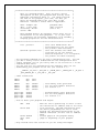
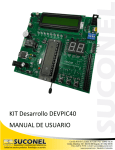
1
Easy PIC Development Board
User Manual
1st Edition
April 2005
How to use this manual.
In an effort to enable PICSTERS with the appropriate skill set needed to make this course as rewarding as
possible, this manual provides detailed information and walks you through the stages of developing your
own codes. This manual is divided into four parts. There is a lot of material here, but you may not use all of
it for your project.
PARTS
I.
The Easy Pic Development Board: Design and Assembly - This part introduces the features of
the Easy Pic Development Board and gives some background information on its design.
II.
Getting Started: Programming the PIC - The second part provides you with a brief review of
assembly language programming and the PIC instruction set. Here you will find a template that
you can use as a starting point for writing your own assembly language program. This part
concludes with instructions on assembling your assembly language program and downloading
object code to the PIC microcontroller.
III.
BootLoader: This part describes how the actual user codes work with the bootloader. This will
explain how to load the bootloader program and how to load the user code on the bootloader.
IV.
The Easy Pic Development Board: In Action - This part contains the information you need to
make your Easy Pic Development Board actually do something. It begins by introducing the
operation of the Easy Pic Development Board in two modes. One mode is bootloader mode and
another one is Programmer mode. It then steps through the features of the PIC microcontroller,
one-by-one, complete with instructions, diagrams, sample code and working examples. Equipped
with the information provided here, you will be able to unleash the full capabilities of the Easy Pic
Development Board.
V.
Appendices - These are referenced by the three previous parts. Feel free to detach the appendices
from the bulk of this manual; you will likely refer to them often.
This manual is intended to be a supplement to the PIC16F877A data sheet. The PIC16F877A data sheet
includes absolutely everything you will need to know about the PIC16F87X microcontroller and this user
manual refers to it often. Another helpful reference is the PICmicro Midrange Reference Manual. I would
sincerely recommend taking the time to read this entire manual from beginning to end and to familiarize
yourself with the data sheet; the things you will learn along the way will be helpful when it comes to
designing your own project. Be aware, however, that completion of this manual will merely lay the
groundwork for more interesting, albeit more useful, applications of the Easy Pic Development Board.
Keep in mind that the Easy Pic Development Board is just the central nervous system of your project. You
are responsible for the design of the extraneous circuits that your project will utilize (sensors, motors,
etc…). It would be prudent to make your initial circuit designs on this Easy Pic Development Board, then
later transfer your design to a PCB CAD; to have it milled into a clean PCB. In general, rats nests of wires
don’t hold up very well and, in accordance with Murphy’s Law, will inevitably let you down when you
need them the most (during demonstrations of course!).
Contributors
This document was created by contributions from: Advanced Embedding and Packing solutions Pvt. Ltd.,
Future Tecknics Pvt. Ltd. and Winnii Solutions Pvt. Ltd. Chennai.
Table of Contents
Part I – The Easy Pic Development Board: Design and Assembly
1.0 Introduction to the Easy Pic Development Board
1.1 Easy Pic Development Board Specifications
1.2 Functional Description
1.2.1 DC Power Supplies
1.2.2 RS-232 Serial Interface
Part II – Getting Started: Programming the PIC
2.0 Programming the PIC Microcontroller
2.1 Assembly Language Programming
2.2 Memory Structure
2.3 Instruction Set
2.3.1 Mathematical Operations
2.3.2 Flow Control
2.4 Subroutines
2.5 Interrupts
2.6 Putting It All Together
3.0 Assembling Your PIC Program
3.1 Developing your PIC program
3.2 Writing Your Program to the PIC
Part III – BootLoader
4.1 Introduction
4.2 How to use the bootloader
Part IV – Easy Pic Development Board: In action
5.0 Peripheral Features
5.1 I/O Ports –PortA,B,C,D & E
5.2 Led
5.3 7Segment
5.4 LCD Device
5.5 Key Switches
5.6 Analog to Digital Converter
5.7 Pulse Width Modulation
5.8 Relay
5.9 Buzzer
5.10 Master Synchronous Serial Port (MSSP)
5.10.1 Serial Peripheral Interface (SPI)
5.10.2 I2C
5.11 Universal Synchronous Asynchronous Receiver Transmitter (USART)
5.12 Timer Modules
Part V - How to use the Easy Pic Development Board
Part I
The Easy Pic Development Board:
Design and Assembly
1.0 Introduction to the Easy Pic Development Board
The Easy Pic Development Board is a compact, low power controller board that is based on the MicroChip
Technologies. This Easy Pic Development Board has a PIC16F877Aseries microcontroller. The PIC is the
heart and soul of the Easy Pic Development Board, containing the central processing unit for the board.
The Easy Pic Development Board will be common to all projects with the addition of student designed and
built circuits.
This Easy Pic Development Board comes loaded with the following features:
Communication Interfaces: RS-232 communication with a PC; SPI and I2C busses for
communicating with other chips; and standard 5V CMOS digital I/O for anything else.
The PIC16F877A Easy Pic Development Board supports Parallel Slave Port Communication.
Extra Features: Three timer modules, a multi-channel analog-to-digital converter, two pulsewidth-modulated outputs, LCD Device, 7Segment Led, Key Switches, Relay, Buzzer and Led.
Additional Features of the PIC16F877 Easy Pic Development Board: Bootloader that allows
you to develop and load your own code to the PIC without the need of Programmer
Two Methods to load the user program to the PIC:
BootLoader mode: BootLoader Mode is very useful for code development. Here Bootloader is
used to load your code to the PIC.
Programmer mode: Programmer mode uses assembly code you have written and then “burned”
to the PIC. This mode uses Programmer.
Complete with a relatively powerful processor and large I/O capability, the Easy Pic Development Board is
an impressive control system. The range of projects is virtually limitless: you can control robots, perform
wireless communication, carry out digital signal processing, or even connect your Easy Pic Development
Board to the Internet. The only limit is your imagination.
Peripheral Features
1)
2)
3)
4)
5)
6)
7)
8)
9)
10)
11)
12)
13)
I/O Ports
LED
7Segment LED
LCD Device
Key Switches
10bit Analog to Digital Converter
Pulse Width Modulation
Relay Operation
Buzzer
SPI Communication
I2C Communication
USART
Timer Modules
1.1 Easy Pic Development Board Specifications
These table lists the electrical characteristics of the Easy Pic Development Board, exceeding maximum
values will very quickly damage your board.
PIC16F877A
Total Number of Pins on PIC (DIP package)
40
Range of Input Voltage to Barrel Connector
6-18 Vdc
PIC Supply Voltage
5 Vdc
Clock Speed
4 MHz (Upgradeable to 20 MHz)*
Digital I/O Pins
33
Analog to Digital Channels
8 (multiplexed)
Pulse Width Modulated Pins
2
10 Pin LCD Interface
Yes
Power Consumption with all IC’s
140 mA @ 16 Vdc
Max current drawn from +12Vdc connector
500 mA
Max current drawn from +5Vdc connector
500 mA
Max current drawn from -12Vdc connector
50 mA
Table 1.1 – Easy Pic Development Board Specifications
1.2 Functional Description
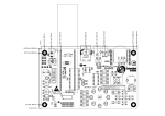
The Easy Pic Development Board is designed in a modular manner as shown in the block diagram below.
Refer to the Easy Pic Development Board schematic and board layout diagrams (found in appendix) as
necessary to improve your understanding.
Figure 1.1 – Block Diagram of the Easy Pic Development Board Design
1.2.1 DC Power Supplies
Figure 1.2 – DC Power Supplies Schematic
DC power is supplied to the board through a 2.1mm coaxial barrel connector with center positive polarity.
Normally this power comes from a 18Vdc 500mA wall adaptor plugged into the barrel connector.
However, a 12Vdc 1A wall adaptor or suitably sized battery array can also be used. The Body or the barrel
is negative supply.
Diodes D1 and D2 provide some reverse polarity protection and power supply transient isolation.
Capacitors C1 and C2 provide power supply bulk charge storage while C3-C6 provide additional power
supply transient isolation for their respective supplies.
IC1 (7805) regulates the bulk supply to the +5Vdc needed for the PIC micro-controller and logic devices
(logic side of MAX232,LCD, 7Seg Display etc). IC2 (7812) and its components regulate the bulk supply
for the Relay.
You will notice that the polarized capacitors have a non-polarized capacitor in parallel with them. This is
not always necessary in designs but is here. The reasoning is that real capacitors are not ideal capacitors:
larger capacitors tend to have greater amounts of intrinsic inductance associated with them due to their
construction. Their greater inductance gives them poorer high frequency performance. Smaller capacitors
tend to have better high frequency performance. Therefore, multiple real capacitors are used to
approximate the required ideal capacitor performance.
1.2.2 RS-232 Serial Interface
The RS-232 circuitry consists of a DB9 female connector, the MAX232 and related circuitry. The DB9
connector is configured for an IBM PC-style 9-pin RS-232 connection. The MAX232 converts the RS-232
(sometimes called the HIN232) +/-12V signals to logic levels for the micro-controller. The resistors (330Ω)
limit line slew rates and provide some short circuit protection. The resistors R23, R24 (not shown here, see
Appendix A – Easy Pic Development Board Schematic Diagrams), R33 and R34 provide output contention
protection (contention is created if the Digital I/O pin of PIC incorrectly configured as an output and is
connected to the output of the MAX232). C24—C25 are used by the on-board charge-pump (note that the
supply is +5V and yet the IC can deliver RS-232 level signals).
Figure 1.3 – RS-232 Serial Interface Schematic
Part II
Getting Started:
Programming the PIC
2.0 Programming the PIC Microcontroller
The main focus of this manual is assembly language programming of the PIC microcontroller. You will
have access to a C compiler in your lab, however, the discussion on programming the PIC in C is limited
and you will likely need to seek other resources.
2.1 Assembly Language Programming
Here we will review some of the basics of assembly language programming. First it is important to
understand the memory structure of the PIC16F877A microcontroller. For detailed information on memory
structure see the PIC16F877A data sheet.
2.2 Memory Structure
There are three memory blocks:
Program memory
Data memory
EEPROM data memory
1.Program Memory
The program memory is, as you may have guessed, the section where your program instructions are stored.
The size of the program memory for the PIC16F877A is 8Kx14 which means that it can hold 8x1024=8192
14-bit instructions.
The program memory is divided into 2K blocks called pages. So it has 4 pages. In order for commands on
a certain program memory page to be executed the corresponding page must be selected. To switch
between program memory pages use the pagesel directive.
A recommended way to use the pagesel directive is to first define the following values at the beginning of
your assembly language program as follows (also see section 3.6):
page0
page1
page2
page3
EQU
EQU
EQU
EQU
0x0000
0x0800
0x1000
0x1800
;
;
;
;
start
start
start
start
address
address
address
address
of
of
of
of
page0
page1
page2
page3
Then to select a page, say page 2 for example, use the following in the body of your main program:
pagesel
page2
; selects program memory page 2
2.Data Memory
The data memory is divided up into 4 banks (bank 0-bank 3) that contain both Special Function Registers
and General Function Registers. The special function registers are named and have a predefined function.
They are used for controlling the operation of the microcontroller. General function registers are used for
data storage. The PIC16F877A has 368 8-bit general function registers.
To access a register in a certain data memory bank you must ensure that the appropriate bank is selected.
The status of the bank select bits, RP0 and RP1 (located in the STATUS register), determine which data
memory bank is active. For example, to access the general-purpose register at address 0xA0 you must
select bank 1 (i.e. RP1:RP0 =01).
The banksel directive can also be used to select the desired data memory bank, similar to the way in which
the pagesel command is used to select the desired program memory page. First define the following
values:
BANK0
BANK1
EQU
EQU
0x0000
0x0080
; Data Memory start positions
BANK2
BANK3
EQU
EQU
0x0100
0x0180
Then to select the bank, say bank1 for example, use the following in the body of your main program:
banksel
BANK1
; select data memory bank 1
3.EEPROM Memory
The EEPROM memory is nonvolatile meaning its contents are not erased when you turn off the power to
the PIC. This is useful for storing information such as the state of your system before it is powered-down
since this information can then be retrieved when the system is powered-up again. Data stored in the Data
memory section (RAM) is erased when the power is removed from the PIC.
2.3 Instruction Set
The PIC16F877A uses a RISC-based architecture with only 35 instructions. See the PIC16F877A data
sheet for instruction descriptions. Some of the more common instructions will be reviewed here.
An instruction is either byte-oriented or bit-oriented. The following bits of a register.
bcf
bsf
STATUS , RP0
STATUS , RP1
; Clear the RP0 bit in the STATUS register.
; Set the RP1 bit in the STATUS register.
; Anything after a semicolon is a comment.
Remember that the RP0 and RP1 bits are used to select the data memory bank. The instructions above will
select bank 1 (i.e. RB0:RB1=01).
The following is an example of a byte-oriented instruction.
clrf
STATUS
; Clear the entire STATUS register.
Many instructions use the ‘W’ register, which you can think of as a temporary storage place. To store a
value in one of the general-purpose registers, say at address 0x20 (in bank 0), you could use the following
commands:
bcf
STATUS , RP0
bcf
STATUS , RP1
movlw
0x35
movwf
0x20
; select bank 0
; writes 0x35 to the W register
; moves the value from the W register to the
; general purpose register at address 0x20
To make your code more readable you can define labels to replace numerical values. These labels are
defined at the beginning of your program using the EQU (equate) assembler directive.
length
lreg
EQU
EQU
0x35
0x20
; Equate the label length with value 0x35.
; Equate the label lreg with value 0x20.
With these defined the above instructions could now be replaced with:
movlw
movwf
length
lreg
; Load the W register with the value 0x35.
; Move the value from the W register to the
; General-purpose register at address 0x20.
An additional benefit to using labels is that if you decide to change any one of the values in your source
code, you need to only change the value of the label rather than having to search through your entire source
code for every occurrence of that value.
2.3.1 Mathematical Operations
Mathematical operations can be difficult since the instruction set includes commands only for addition and
subtraction and there are no hardware floating-point operations. If you require this functionality in your
code, there are some software emulation libraries that can be found on the microchip Webster
(www.microchip.com), but they are not always easy to find. Try a search for ‘math emulation’. When
programming in C, many of the advanced math functions are available to you.
addwf
lreg , W
; Add the contents of W and lreg and stores
; the result in W.
Here the W register is the destination for the result of the addition, as specified by the second argument to
the instruction. Alternatively, you can specify lreg to be the destination register by replacing W with F
(file).
addwf
lreg , F
; lreg is now the destination register
2.3.2 Flow Control
You can control the flow of your program using conditional or unconditional branches. Conditional
branches (i.e. btfss, btfsc, incfsz, decfsz) test the value of the operand and branch accordingly. An
example of an unconditional branch is the goto instruction.
A useful technique to use with flow control is ‘labeling’. You can label locations in your program and
branch to that location using the label name. For example:
bcf
bcf
STATUS , RP0
STATUS , RP1
; Select bank 0.
decfsz
lreg , F
goto
goto
LOOP
ZERO
;
;
;
;
;
LOOP
Decrement the value in the lreg
register and skips the next
instruction if the result is 0.
Branch to LOOP if result not 0.
branch to ZERO if result is 0.
:
ZERO
{instructions}
:
2.4 Subroutines
Using subroutines is a way to make your program modular. It also shortens the length of your main
program making it easier to follow.
You can think of subroutines as mini programs that are called from the main program. Subroutines are
usually defined after the main program. Consider the code below:
main
{main program instructions}
:
call incW
; call incW subroutine
:
goto main
; return to beginning of main program
; subroutines are declared here
incW
incf
incf
incf
W
W
W
return
; increment the value in the W register 3 times
; return to main program
Here a subroutine called incf W is defined. The purpose of the subroutine is to increment the value in the
W register 3 times. In the main program you call the subroutine using the call instruction with the
subroutine name as the operand. When the call command is executed the main program jumps to the incf
W subroutine, executes the commands defined there, then returns to the main program when the return
instruction is executed.
Unlike many other microcontrollers, the PIC contains no user-accessible stack. Adding the fact that the
programmer’s model contains only one working register, subroutines passing more than a single byte need
to make use of the file register memory. Additionally, the stack in the PIC16F877a devices is only 8
locations deep. Recursive calling is thereby discouraged. Interrupts, described next, also require stack
locations and reduce the possible call-depth.
2.5 Interrupts
Interrupts are an alternative to polling for events and can make processing time more efficient, since your
program doesn’t need to wait for selected events to occur by polling. Every time a selected event triggers
an interrupt, the PIC stops execution of the program and jumps to the interrupt service routine. Once
finished, the PIC resumes normal execution of your program, where it left off.
Each of the built-in modules has the ability to cause an interrupt for one reason or another. The ADC, for
example, can cause an interrupt when it has completed a conversion while the UART can produce an
interrupt when its transmit buffer is empty or when its receive buffer is full.
When an interrupt occurs, the PIC jumps to the program memory location 0x0004, the interrupt vector. The
program space available in this location is very limited so it’s recommended that you place your interrupt
service routine (ISR) elsewhere in program memory and just put a GOTO command in the interrupt vector
space.
For Ex:
ORG
Goto
ORG
Goto
0X0000
Start
0X0004
Isev
Start
Write your codes here
Isev
Write your Interrupt subroutine here
End
Compared with other microcontrollers, the PIC16F877A family has a few notable differences with respect
to interrupt processing.
1. Only one interrupt vector is used. Your ISR must determine (through status bits) which subsystem
generated the interrupts.
2. Context of the CPU is not saved, except for the return Program Counter. Your ISR must be written to
compensate for this.
3.Each interrupt uses one internal stack location until processing is complete. Only 8 stack locations are
available and subroutine calls also use them. Due to this limitation, use of nested interrupts is discouraged.
However, nesting is disabled by default.
2.6 Putting It All Together
Now you are almost ready to write our own PIC assembly program. You can use any text editor to write
your source code as long as you save it with a .asm extension. It is recommended that you use MPLAB, a
free program provided by Microchip, to write and compile your source code. You can download a copy of
MPLAB from the Microchip website (www.microchip.com) .
Below is a very simple program that is used to show the necessary components for an assembly program.
Also, MPLAB contains source code templates (f873temp.asm and f877temp.asm), which can be found in
mplab/template/code/. You can use these as a starting point.
;************************************************************
;
*
;
This is a program header. Here you give a brief
*
;
description of what your program does and any other
*
;
important information about it. You should include
*
;
the name of the program, your name, the date you
*
;
wrote the program and/or the last date it was
*
;
modified. Include a course name if applicable.
*
;
*
;
name: example.asm
(program name)
*
;
date: 9 July 2002
(date created)
*
;
created by: Murali
(that’s me)
*
;
course: EEE
*
;
*
;
This program doesn’t do anything (since there are no *
;
instructions in the main program). It is just used
*
;
to illustrate the necessary components of an assembly *
;
language program for the PIC microcontroller.
*
;
*
;************************************************************
list
p=16f877
#include <p16f877.inc>
;
;
;
;
;
;
;
;
;
;
;
;
;
this tells MPLAB which PIC
microcontroller you are using.
use p=16f877 when necessary.
this file defines the names and
locations of all the Special
Function Registers (i.e. W register)
use p16f877.inc when necessary.
The following commands set the PIC’s configuration bits. For now
you don’t really need to understand how the configuration bits
affect anything, but if you really want to see section 12.1 in the
PIC16F87X data sheet.
You can also set the configuration bits manually when you are
downloading your program to the PIC (see section 4.1)
__CONFIG _CP_OFF & _WDT_OFF & _BODEN_OFF & _PWRTE_OFF & _XT_OSC &
_WRT_ENABLE_ON & _LVP_OFF & _CPD_OFF
; Label Definitions
TEMP1
TEMP2
EQU
EQU
0x20
0x21
BANK0
BANK1
BANK2
BANK3
EQU
EQU
EQU
EQU
0x0000
0x0080
0x0100
0x0180
page0
page1
page2
page3
EQU
EQU
EQU
EQU
0x0000
0x0800
0x1000
0x1800
; Data Memory start positions
; for use with banksel directive
; see section 3.2
; program memory start positions
; for use with pagesel directive
; see section 3.2
; This is where your program code begins
ORG
0x00
movlw 0x00
movwf PCLATH
goto Main
nop
;
;
;
;
;
;
;
;
;
;
when the PIC is powered up or after a reset
the instruction at address 0x00 is the first
to be executed. The ORG instruction tells
the device programming the PIC to start
writing the following instructions at the
address indicated (in this case at address
0x00).
selects page0 of the program memory
jumps to beginning of your program
; Only include this next section if you are using interrupts.
ORG
0x04
goto
Service
;
;
;
;
when an interrupt occurs the program jumps
to the instruction at address 0x04
jumps to the subroutine ‘service’, which will
handle the interrupt.
; this is the start of your main program
Main
{the instructions for your main program go here.}
; this is the interrupt service routine
Service
{the instructions for your interrupt service routine go here.}
END
; this is the end of the program.
The source code for some example programs is available on the CD Disk. It may help to take a quick look
at the code to become more familiar with the contents of an assembly language program.
3.0 Assembling Your PIC Program
It has the following two parts.
3.1 Developing Your PIC Program
To actually make your Easy Pic Development Board “do” anything, it needs to be running a program. In
this section you will use MPLAB to develop your own assembly code. In the next section you will burn the
program’s object code to your Easy Pic Development Board.
To develop and assemble the program, follow these steps:
1.
2.
3.
4.
5.
6.
Open MPLAB
Create New Project ( Project New)
Create New File (File New)
Write Your assembly code
Add your source code to the Project. (Project Add files to project)
Compile your source code. (Project
Build All)
And that’s it. A new window will open that shows the results of the process. If your source code is error
free the message ‘Build Completed Successfully.’ will appear in this window. Assembling generates a
*.hex file and places it in the same directory as your source code file. This is the file that you will
download to the PIC microcontroller. You can also copy the *.hex file from the Disk.
If there are errors in your code then this window will contain the appropriate error messages.
3.2 Writing Your Program to the PIC
The PIC has a flash type program memory, which can be written, erased and rewritten. This is very useful
for debugging (you can test out the capabilities and connections of your circuitry before letting your project
run amuck). Typically the flash memory can go through several thousand of these cycles so you don’t need
to worry about it breaking down on you.
Here we are providing two methods to burn a program to the PIC. These are Bootloader mode, programmer
mode. Bootloader mode is explained in the next Section. In this section you will see the Programmer mode.
You should buy any programmer to burn your program to the PIC. Before using the Programmer, you
should read the manual given with it. The manual describes how to put the PIC on the Socket. The position
where you place the PIC is very important. If you do anything wrong that will permanently damage your
Programmer and destroys your PIC.
They will provide the user-friendly software to do the following
Select the PIC to burn
Select the hex file
Configure the PIC
Erase the codes in the PIC
Read the PIC
Burn the program to the PIC
Using the software burn the program to the PIC. You will receive a message notifying you if the program
was transferred to the PIC successfully. Take the PIC out of the Programmer, plug it backs into your Easy
Pic Development Board, and you’re ready for business.
Part III
PIC 16F8xx Boot Loader
4.0 Introduction
A bootloader is used to quickly download a new program into your PIC micro, in a few seconds. Once you
have it set up, you can quickly update the .hex file in your PIC micro with a single keystroke. Bootloading
is easily performed in-circuit, with the PIC micro still plugged into your PCB.
BootLoader reserves top 255bytes in the Program memory. If you use this bootloader, you can’t use the
upper 255 bytes for your normal program. As well as you should also include the following four additional
lines in your assembly program.
Org
Movlw
Movwf
Goto
Nop
0x0000 (These four lines should be included)
0x00
PCLATH
Main
Org
Goto
Main
0x0004 (Optional)
Isev
:
:
Isev
:
:
End
For CCS C language you don’t need to include any additional lines.
4.1 How to use the BootLoader
•
•
•
•
•
•
•
•
•
•
•
•
•
•
The PIC 16F877A that we have given to you has already programmed with the bootloader code. If any
case it lost, load bootloader.hex file to the PIC. For this purpose you should use any programmer.
Put that PIC on the Zip Socket on the given board.
Plug in the RS232 serial adapter to your Board.
Give the power supply to the board.
Use MPLAB for your code creation and corrections.
Compile with MPLAB to produce *.Hex file
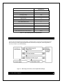
If finished, open PIC Bootloader+ Software. ( BootL Sw\PICbootPlus.exe) That window is look like
the below figure.
Set baud rate is 9600.
Select the Com Port which will be used (you will need one free com port on your system).
Click the search button to select your .hex file.
Click Write button on the window software, then press the reset key on the board to burn your hex file
to the PIC
If everything is ok, you will see the OK message in the info box.
The bootloader remains active for 0.2 seconds after reset, to give you the option of uploading new
code, and after 0.2 seconds (or uploading complete) you can use the serial port as normal and also it
executes the user code.
If not, it will display the relevant error message
Figure: BootLoader
Part IV
The Easy Pic Development Board
in Action
5.0 Peripheral Features
This section will explain the features of the Easy Pic Development Board. It has following features
1)
2)
3)
4)
5)
6)
7)
8)
9)
10)
11)
12)
13)
I/O Ports
LED
7Segment LED
LCD Device
Key Switches
10bit Analog to Digital Converter
Pulse Width Modulation
Relay Operation
Buzzer
SPI Communication
I2C Communication
USART
Timer Modules
5.1 I/O Ports
The PIC16F877 has 33 I/O pins, divided into 5 ports (Port A-Port E), which can be configured in various
ways to communicate with many different peripheral devices. Port A has 6 pins, Port B-Port D each have 8
pins and Port E has 3 pins.
Many of these pins are multiplexed with more than one function. You can control the function of each pin
(or group of pins) by writing the proper value to the appropriate Special Function Register.
The simplest function for these pins is general purpose digital I/O. You can configure any pin as a digital
output and set its value high (+5V) or low (0V), or configure it as a digital input and read its present value.
Each port has an associated PORTx register (bi-directional port) and a TRISx register (data direction
register). Setting a bit in the TRISx register makes the corresponding pin an input, clearing the bit makes it
an output. For example, setting bit 4 in the TRISB register makes pin RB4 an input. Setting a bit in the
PORTx register sets the corresponding pin high (as long as it is configured as an output). Clearing the bit
set the pin low. For example, setting bit 3 in the PORTC register sets the output pin RC3 high. Data is
input by reading from the PORTx register.
The following code is an example of how to implement this in your program.
bsf
bcf
STATUS , RP0
STATUS , RP1
; select bank1
movlw
movwf
B’11110000’
TRISB
; configure RB7:RB4 as inputs
; configure RB3:RB0 as outputs
bcf
STATUS , RP0
; select bank0
movf
PORTB , W
; reads inputs and stores in W register
movlw
movwf
B’1010’
PORTB
; sets outputs RB3 and RB1 high,
; RB2 and RB0 low
Each port, and the alternate function(s) of its pins, is discussed in its own section below. Refer to section
3.0 of the PIC16F87X data sheet for additional information on I/O ports.
5.1.1 Port A
In this section port A is discussed. It is multiplexed with analog inputs (with the exception of pin RA4,
which is multiplexed with the Timer0 module). Instead of Port A, Port E is also multiplexed with analog
inputs but in this board these pins are used to control Relays and Buzzer. So you have only 5 analog
channel instead of 8. In these five channels, 3 channels are connected internally and analog voltage is
controlled through POT. The remaining two channels is used for the external analog input.
The function of each pin in this port is selected using the A/D port configuration control bits (the lower four
bits of the ADCON1 register). Refer to Section 11.0 (Register 11-2) in the PIC16F877A data sheet for a
table of the A/D port configuration control bits.
For example, to configure all the pins in ports A and E for general purpose digital I/O you must write
B’011x’ (B’0110’ or B’0111’) to the lower four bits of the ADCON1 register.
The analog inputs are used with the Analog-to-Digital Converter (A/D) module. See section 6.7 for
instructions on using the A/D module. The ADON bit (ADCON0<0>) controls whether or not the A/D
module is operating. If you are not using the A/D module then it is recommended that you turn it off by
clearing the ADON bit.
Data is read from/written to ports A and E using the PORTA and PORTE port registers, respectively. The
data direction registers are TRISA and TRISE.
Table 6.1: Summary of Registers Associated with PORTA.
The following code shows how ports A can be initialized for digital I/O:
bcf
bcf
STATUS , RP0
STATUS , RP1
clrf
PORTA
bsf
bcf
STATUS , RP0
STATUS , RP1
movlw b’0110’
movwf ADCON1
movlw b’111000’
movwf TRISA
; select bank0
; clear ports A to initialize
; select bank1
; configure ports A and E for
; digital I/O
; set RA5:RA3 and RE0 as inputs
; RA2:RA0 and RE2:RE1 as outputs
5.1.2 Port B
Port B is a general purpose Digital I/O Port. Data is read from/written to port B using the PORTB port
register. The data direction register.This Port is multiplexed with following function
•
•
•
Glow the led in output mode
Get the input through Key Switches
Control the multiplexed 7Segment LED
This Port has following features
♦ Support External Interrupt in RB0
♦ Support the interrupt-on-change in RB4-RB7
Table 6.2: Summary of Registers Associated with PORTB.
Name
Address
Bit 7
Bit 6
Bit 5
Bit 4
PORTB
0x06
RB7
RB6
RB5
TRISB
0x86
OPTION_REG
0x81
RBPU
INTEDG
T0CS
Bit 3
RB4
RB3
PORTB data direction bits.
T0SE
PSA
Bit 2
Bit 1
Bit 0
RB2
RB1
RB0
PS2
PS1
PS0
5.1.3 Port C
Port C is shared by many of the peripheral functions, such as the timer modules, the pulse-width-modulator,
the analog-to-digital converter and the serial communication modules
Data is read from/written to port C using the PORTC port register. The data direction register is TRISC.
Table 6.3 Summary of Function Associated with PORTC
No
1
2
3
4
Port Pins No
RC1,RC2
RC0,RC3-RC5
RC3,RC4
RC6,RC7
Functions
Pulse Width Modulation
SPI
I2C
USART
Table 6.3: Summary of Registers Associated with PORTC.
Name
Address
Bit 7
Bit 6
Bit 5
PORTC
0x07
RC7
RC6
RC5
TRISC
0x87
Bit 4
Bit 3
RC4
RC3
PORTC data direction bits.
Bit 2
Bit 1
Bit 0
RC2
RC1
RC0
5.1.4 Port D
Port D is multiplexed with the Parallel Slave Port (PSP) module. To disable the PSP module the
PSPMODE bit (TRISE<4>) must be cleared.
Name
Address
Bit 7
Bit 6
Bit 5
PORTD
0x08
RD7
RD6
RD5
TRISD
0x88
TRISE
0x85
IBF
OBF
IBOV
Bit 4
Bit 3
RD4
RD3
PORTD data direction bits.
PSPMODE
Table 6.4: Summary of Registers Associated with PORTD.
Bit 2
Bit 1
Bit 0
RD2
RD1
RD0
PORTE data direction bits.
In this board PORTD is multiplexed with LCD Device and 7Segment LED.LCD Device uses RD0-RD6
pins (RD0-RD3 Control Lines (Rs, Rw and Es), RD4-RD6 Data Lines). Here this board has
multiplexed six 7segment LED. This uses Port D for data line and Port B for segment selection.
Data is read from/written to Port D using the PORTD port register. The data direction register is TRISD.
5.1.5 Port E
Port E is multiplexed with analog input. But here these pins are dedicated to some other application like
Relay operation (RE0, RE1) and Buzzer (RE2).
Data is read from/written to Port D using the PORTD port register. The data direction register is TRISD
Table 6.4: Summary of Registers Associated with PORTE.
5.2 LED
In this board Led is connected in Port B. LED is used to indicate the pin status. There is a Jumper to enable
or diable the Led’s.
Program which uses the LED function:
Assembly File
Flash.asm (Example\Flash.asm)
Shifting.asm (Example\Shifting.asm)
Hex File
Flash.hex (Example\flash.HEX)
Shifting.hex (Example\shifting.HEX )
5.3 7Segment LED
Here we have six 7Segment Led. These are multiplexed with one another. This function uses Port D and
Port B. Port D is used to send the data to the Segment and Port B is used to select the particular Segment to
Glow.
You have already known the 7Segments are multiplexed with the LCD. Before proceeding it you should
select 7segment display by changing the jumper to 7Seg position (See the Easy Pic Development Board).
Port B is multiplexed with the keyswitches, so changing the jumper to LED position
Program which uses the 7Segment LED function:
Assembly File
7segment.asm (Example\7Segment.asm)
Multiplex.(Example\Multiplexing.asm)
Arith.asm (Example\arith.asm)
Adc.asm (Example\Adc_volt.asm)
Hex File
7segment.hex (Example\count.HEX)
Multiplex (Example\Multiplexing.HEX)
Arith.hex (Example\arith.HEX)
Adc.hex (Example\Adc_volt.HEX )
Load the hex file to the PIC and see the output. If anything goes wrong check the power socket,& Jumper
position.
5.4 LCD Device
Now you knew this device is multiplexed with 7Segment.And you also knew it uses Port D for both control
and data lines. Before using this device you should change the jumper position to LCD Device. (See the
Board)
Program which uses the LCD function:
Assembly File
Lcddisplay.asm (Example\LcdDisplay.asm)
Acd_lcd.c (Example\Adc_Lcd.c)
Scanning.c (Example\AdcScan.c)
Eeprom.asm (Example\EepromLcd.asm)
Hex File
Lcddisplay.hex (Example\LcdDisplay.HEX)
Acd_lcd.hex (
Scanning.hex (Example\AdcScan.HEX)
Eeprom.hex (Example\EepromLcd.HEX)
5.5 Key Switches
Key Switches are multiplexed with 7segment devices. Key switches are connected from RB0-RB5. You
can use this key switches after changing the jumper to key position (See the Board).
Program which uses the Key Switches:
Assembly File
RB0interrupt (Example\RB0Interrupt.asm)
stopwatch (Example\StopWatch.asm)
Scanning.c (Example\AdcScan.c)
Hex File
RB0interrupt (Example\RB0interrupt.HEX)
Stopwatch (Example\StopWatch.HEX)
Scanning.hex (Example\AdcScan.HEX)
5.6 Analog to Digital Converter
The PIC 16F877A has 8 channels, 10bit Analog to Digital Converter. These eight channels are multiplexed
together; the ADC can only sample one input at a time. Here Port A has five channels and Port E has
remaining 3 channels. But in this board Port E pins are used for some other purposes, so you can use only
PortA analog pins.
In this board 3 channels are directly connected with internal circuit Power through a Variable POT. The
POT is used to change the analog input voltage given to the pin. The other two channels are used to scan
the external analog inputs. You should take care about the external input; its range should be in between 05V DC.
The entire ADC pins have a limited amount of diode protection to prevent input voltages outside of the
Vdd to Vss range. A better way to make sure your PIC doesn't get fried by stray analog voltages though, is
to set up a small circuit before the signal reaches the ADC pin similar to the one to the right. This circuit
will not let any voltage hit the ADC pin unless it is between 0 and 5V and doesn't depend on the PIC's
limited protection.
The PIC16F877A data sheet also recommends that the maximum input impedance of an analog source be
less than 10kΩ and that any current on any pin should not exceed ±20mA.
ADC converts the given analog inputs to the 10bit digital output. It is stored in the register ADRESH,
ADRESL. This conversion uses TRISA, PORTA, ADCON0 and ADCON1 register. Refer 16F877A
datasheet for further need
Program which uses the ADC:
Assembly File
Adc.asm (Example\Adc.asm)
Acd_lcd.c (Example\Adc_Lcd.c)
Scanning.c (Example\AdcScan.c)
Relay.asm (Example\Relay.asm)
Adc_volt (Example\Adc_volt.asm)
Hex File
Adc.hex ( Example\adc.HEX)
Acd_lcd.hex (
Scanning.hex (Example\AdcScan.HEX)
Relay.hex (Example\Relay.HEX)
Adc_volt (Example\Adc_volt.HEX)
5.7 Pulse Width Modulation
You can think of the Pulse Width Modulator as a square wave generator where the period and duty cycle
are variable. There are 2 PWM outputs (CCP1 and CCP2) and they may have different duty cycles but
they share a common period.
The PWM period is calculated using the following formula:
You have control over the value in the PR2 register (Timer2 module’s register) and the TMR2 prescale
value. PR2 holds an 8-bit number and TMR2 prescale value can be either1, 4 or 16. TMR2 prescale value
is set using the T2CKSP1:T2CKSP0 bits (T2CON<1:0>). See section 7.0 (Register 7-1) in the PIC16F87X
data sheet. Tosc is the oscillator period (0.25 μs).
For example, if PR2 contains B’01100111’ = 103 and T2CKSP1:T2CKSP0 = B’01’ (prescale = 4) then the
PWM period is (103+1)*4*0.25*4 = 416 μs.
The duty cycles are specified with a 10-bit number. Each PWM pin has an associated CCPRxL register and
CCPxCON register. The CCPR1L register holds the upper 8 bits of the duty cycle value for CCP1 and
CCP1CON<5:4> holds the lower 2 bits. For CCP2 the CCPR2L and CCP2CON registers are used. The
following equation defines the PWM duty cycle:
For example, if CCPR1L contains B’00110011’ and CCP1CON<5:4> contains B’10’ the duty cycle for
CCP1 is 206*0.25*4 = 206 μs.
Program which use the PWM:
Assembly File
Pwm.asm (Example\Pwm.asm)
Hex File
Pwm.hex (Example\Pwm.HEX)
5.8 Relay
The PIC has a 25mA current drive capability and this current is quite good for most low power circuits.
Sometimes a component like a motor or light bulb may need to be controlled by a PIC output pin and more
than likely, these types of components will draw more than 25mA which can be supplied by the PIC pin.
Figure: Relay
One way around this problem is to use a relay to switch the high currents needed. In some cases, a relay can
be connected directly to the PIC, but usually a transistor is used. A transistor requires only a small base
current to let a much larger current flow through it’s collector. Also, the component that the transistor is
switching can have an operating voltage higher than the 5 volts supplying the PIC. This makes it an ideal
component to control relays from the IO pins of the PIC.
The relay supplied with this board has an operating voltage of 12 volts.
Program which use the Relay:
Assembly File
Relay.asm (Example\Relay.asm)
Hex File
Relay.hex (Example\Relay.HEX)
5.9 Buzzer
Buzzer is connected in the pin RE2. Normally Buzzer is used to indicate some status to the user.This pin
can be activated in your programs to audiable indications, like pressing of a key, confirmation, error etc.
Programs which use the Buzzer:
Assembly File
Buzzer (Example\Buzzer.asm)
Hex File
Buzzer (Example\Buzzer.HEX)
5.10 Master Synchronous Serial Port (MSSP)
The Master Synchronous Serial Port (MSSP) module is used for serial communication with peripheral
devices. The MSSP module can operate in one of two modes:
1.
2.
Serial Peripheral Interface (SPI)
Inter-Integrated Circuit (I2C)
These modes are multiplexed with each other. So you can use only one mode at a time. Before using
MSSP, you should remove the I2C or SPI ADC as appropriate. (see the board).
5.10.1 SPI
The SPI mode allows 8 bits of data to be synchronously transmitted and received simultaneously. All four
modes of SPI are supported. To accomplish communication, typically three pins are used:
• Serial Data Out (SDO) - RC5/SDO
• Serial Data In (SDI) - RC4/SDI/SDA
• Serial Clock (SCK) - RC3/SCK/SCL/LVDIN
Additionally a fourth pin may be used when in a Slave mode of operation:
• Slave Select (SS) - RA5/SS/AN4
SPI mode uses following register:
• MSSP Control Register (SSPCON)
• MSSP Status Register (SSPSTAT)
• Serial Receive/Transmit Buffer (SSPBUF)
• MSSP Shift Register (SSPSR) - Not directly
SSPCON and SSPSTAT are the control and status registers in SPI mode operation. The SSPCON register
is readable and writable. The lower 6 bits of the SSPSTAT are read only. The upper two bits of the
SSPSTAT are read/write. SSPSR is the shift register used for shifting data in or out. SSPBUF is the buffer
register to which data bytes are written to or read from.
In receive operations, SSPSR and SSPBUF together create a double-buffered receiver. When SSPSR
receives a complete byte, it is transferred to SSPBUF and the SSPIF interrupt is set. During transmission,
the SSPBUF is not double buffered. A write to SSPBUF will write to both SSPBUF and SSPSR.
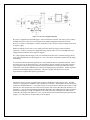
This board has ADC MCP3202 to explain SPI operation. You can connect any other SPI device with the
SPI pins. Before that you should remove the ADC MCP3202 from the IC socket. (See the Board).
Let us see how the SPI device connected with SPI pins:
External ADC (MCP3202) is a 12-bit analog-to-digital converter. There are two input channels available on
the MCP3202.Both the inputs are multiplexed together, the ADC can read only one input at a time.
Using the SPI, MCP3202 is connected to PIC16F877A. Pin Diagram of MCP3202 and Function of each
pin is as follows:
Figure 6.2: MCP3202 Pin Diagram
Figure 6.3: MCP3202 Pin Function Table
Consider the following schematic:
Figure 6.4: Schematic – External ADC Using SPI
The above schematic explains how to connect the external peripheral to the PIC. You should read the
datasheet for peripheral before using it.
Programs which use the SPI Function:
Assembly File
Adc Example\ExternalAdc.asm
Hex File
Adc (Example\ExternalAdc.HEX)
5.10.2 I2C
The MSSP module in I2C mode fully implements all master and slave functions (including general call
support) and provides interrupts on START and STOP bits in hardware to determine a free bus (multimaster function). The MSSP module implements the standard mode specifications, as well as 7-bit and
10-bit addressing.
Two pins are used for data transfer:
• Serial clock (SCL) - RC3/SCK/SCL
• Serial data (SDA) - RC4/SDI/SDA
The user must configure these pins as inputs or outputs through the TRISC<4:3> bits.
The MSSP module has six registers for I2C operation. These are:
• MSSP Control Register (SSPCON)
• MSSP Control Register 2 (SSPCON2)
• MSSP Status Register (SSPSTAT)
• Serial Receive/Transmit Buffer (SSPBUF)
• MSSP Shift Register (SSPSR) - Not directly accessible
• MSSP Address Register (SSPADD
Please refer the PIC datasheet for more information. It uses only two pins. Please remove the SPI device
(ADC MCP3202 ) from the board. This board has an EEPROM (24LS256) I2C device. Also you can
connect any number of peripheral that support the I2C communication. This EEPROM (24LS256) I2C
device is configured as device 1.
Programs which use the I2C Function:
Assembly File
I2C (Example\i2c_24lc256.HEX)
Hex File
I2C (Example\i2c_24lc256.HEX)
Load the above hex file to the PIC and check the result.
5.11 Universal Synchronous Asynchronous Receiver Transmitter (USART)
The Universal Synchronous Asynchronous Receiver Transmitter (USART) module is one of the two serial
I/O modules. (USART is also known as a Serial Communications Interface or SCI.) The USART can be
configured as a full duplex asynchronous system that can communicate with peripheral devices, such as
CRT terminals and personal computers, or it can be configured as a half duplex synchronous system that
can communicate with peripheral devices, such as A/D or D/A integrated circuits, serial EEPROMs etc.
The USART can be configured in the following modes:
• Asynchronous (full duplex)
• Synchronous - Master (half duplex)
• Synchronous - Slave (half duplex)
Bit SPEN (RCSTA<7>) and bits TRISC<7:6> have to be set in order to configure pins RC6/TX/CK and
RC7/RX/DT as the Universal Synchronous Asynchronous Receiver Transmitter. The USART module also
has a multi-processor communication capability using 9-bit address detection.
Program which use the USART Function:
Assembly File
Usart.asm (Example\Usart.asm)
Hex File
Usart.hex (Example\Usart.HEX)
In this example the USART module will be used to communicate with a personal computer.
HyperTerminal (or other terminal program) on your PC is used to communicate with the Easy Pic
Development Board.
Easy Pic Development Board is connected using a computer serial cable. The male end of the cable
connects to the DB-9 connector on your Easy Pic Development Board and the female end connects to one
of the serial connectors (COM1 or COM2) on the back of your PC.
To properly communicate, both the HyperTerminal and the USART must be configured with the same
settings. The below example program uses 9600 baud rate.
The mode of communication is Asynchronous since there is no clock signal. Instead start and stop bits are
used. When asynchronous mode is selected the USART automatically attaches start and stop bits to the
data.
We will only be sending byte size data chunks so 8-bit transmit and receive is selected. Hardware flow
control will be used.
Now open and configure HyperTerminal with the following settings (refer to section 5.0 if necessary).
1.
2.
3.
4.
5.
9600 Bits Per Second.
8 Data Bits.
No Parity.
1 Stop Bits.
Hardware Flow Control.
Load the above program to the PIC and watch the output.
5.12 Timer Modules
Built into the PIC are three timer modules. Timer 0 is a general-purpose 8-bit timer/counter. Timer 1 is a
16-bit timer/counter that can be used with the capture/compare/PWM module. Finally, timer 2 is an 8-bit
timer that is used to control the PWM module. Refer to sections 5-7 in the PIC16F87X data sheet for
detailed instructions on using the respective timer modules.
Program which use the Timer:
Assembly File
Buzzer (Example\Buzzer.asm)
Pwm (Example\Pwm.asm)
Stopwatch (Example\StopWatch.asm)
Hex File
Buzzer (Example\Buzzer.HEX)
Pwm (Example\Pwm.HEX)
Stopwatch (Example\StopWatch.HEX)
6.0 How to use the Board
Here we have given PIC 16F877A datasheet and Easy Pic Development Board Manual, Read the
documents carefully. As well as we have provided some example files to you. Load the .hex file to the PIC
using the Bootloader software (Refer Part III).
1)
2)
3)
4)
5)
6)
7)
8)
9)
Check the jumper position (see Board feature- for LCD, LED, 7Seg & Key Switch).
Connect the RS232 cable connector to the Board Port and free com port of computer.
Connect the power / wall adapter.(18VDC, Barrel Ground, 500ma)
Upload the * .hex file to the PIC through Bootloader software.
Check for user file execution by the PIC.
To view the source code, open *.asm file in Mplab.
Make correction to *.asm file if necessary.
Compile source code with Mplab.
Repeat steps 4 to 8 as needed.