1
Timing characteristics
SPEAr600
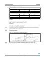
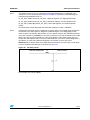
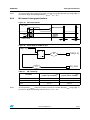
Therefore, we have to add the value T to the clock path and the value T/2 to the command
path.
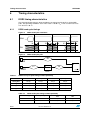
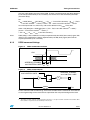
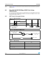
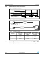
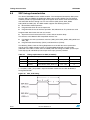
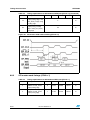
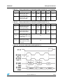
The waveform shown in Figure 8 refers to the pad or memory side, so the CLK edges are
centered on the command valid window. In this case, we consider the minimum values for t4
and t5 in order to obtain the minimum command valid window. We can consider t4 as the
tSETUP of the commands that can be defined as the time range where the commands are
stable before the arrival of the clock. To have a positive quantity the delay obtained by the
commands (maximum delay or last variation) must be less than the one obtained by the
clock (minimum delay).
So:
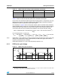
t4MIN = CLK (delay) MIN - CMD (delay) MAX =(T + t3MIN) - (T/2 + t2MAX) = T/2 - t2MAX + t3MIN
t5 can be expressed in a similar way, and can be defined as the tHOLD of the commands:
t5MIN = CMD (delay)MIN - CLK (delay)MAX = (T + T/2 + t2MIN) - (T + t3MAX) = T/2 - t3MAX
+t2MIN
Note:
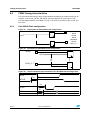
CLK(delay) is the combination of delays experienced by the CLK signal, CMD(delay) is the
combination of delays experienced by the command/ctrl/address signal (both until the
capture performed by the memory).
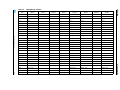
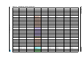
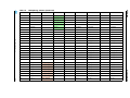
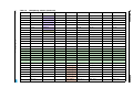
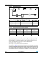
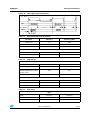
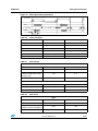
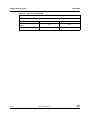
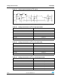
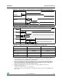
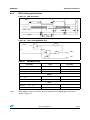
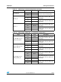
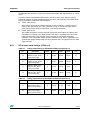
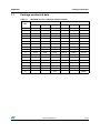
Table 35.
DDR2 command timings without pad delay
Period (T)
Frequency
t4MIN
t5MIN
3 ns
333 MHz
977 ps
1.33 ns
3.75 ns
266 MHz
1.35 ns
1.71 ns
5 ns
200 MHz
1.98 ns
2.33 ns
6 ns
166 MHz
2.49 ns
2.84 ns
7.5 ns
133 MHz
3.23 ns
3.59 ns
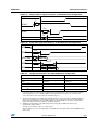
Table 35 shows the internal chip timing without the contribution of the pads.
64/97
Doc ID 16259 Rev 3