1
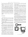
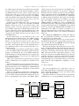
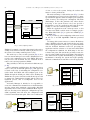
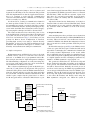
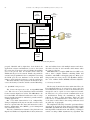
Microprocessors and Microsystems 31 (2007) 77–86
www.elsevier.com/locate/micpro
Secure IP downloading for SRAM FPGAs
q
J. Castillo *, P. Huerta, J.I. Martı́nez
DIET, DAC, Universidad Rey Juan Carlos, Dep. II, D. 157, C/ Tulipan S/N, Móstoles, Spain
Available online 28 February 2006
Abstract
Nowadays there is a growing number of systems based on FPGAs spread over wide areas. When these kind of systems are used, serious security problems may appear. The configuration data for these devices can be very sensitive information that has to be protected
against piracy and reverse engineering.
In this paper, the main target is to describe a rapid prototyping platform that allows Secure IP downloading and Rights Management.
This platform is based on the possibility offered by the new FPGA families for reprogramming part of the device while the rest is working. This work shows how an FPGA system based on an Open Source OpenRISC 1200 microprocessor takes advantage of this feature to
perform the Secure Download of the software and the hardware needed to run a User Application. The platform includes digital signature schemes, symmetric encryption and hashing functions to increment the security. An IP rights management method using this architecture is also presented.
Ó 2006 Elsevier B.V. All rights reserved.
Keywords: FPGA; Secure configuration; On the field configuration; Partial reconfiguration; Self-reconfiguration; Right management
1. Introduction
Nowadays there are a great number of electronic systems distributed over a wide area, for example, a set of
net routers in a country or a group of cash points in a city.
The growth of the FPGA capabilities has significantly
increased the use of FPGA-based systems.
It is not difficult to see that the combination of these two
factors can lead to a set of potential problems not completely covered today.
These problems can be classified in:
Local security. An attacker could have physical access to
the system. Two different types of attacks against the IP
can be achieved: cloning and reverse engineering. Therefore, it is necessary to strengthen the confidentiality of
the design contained inside the FPGA.
q
This work has been supported by the Spanish PROFIT and European
MEDEA+ program under FIT-0700000-2003-930 contract.
*
Corresponding author.
E-mail addresses: [email protected] (J. Castillo), pablo.huerta@
urjc.es (P. Huerta), [email protected] (J.I. Martı́nez).
URL: http://escet.urjc.es/~jmartine (J.I. Martı́nez).
0141-9331/$ - see front matter Ó 2006 Elsevier B.V. All rights reserved.
doi:10.1016/j.micpro.2006.02.001
Secure upgrades. One of the most important features of
an FPGA is the reconfiguration capability that makes possible to remotely update the design or to correct a bug. But
during the updating, an attacker could have access to the
configuration data of the FPGA or the transmission of
the data could fail by any other causes. Therefore, it is necessary a mechanism to download in a secure way new or
updated designs to a remote FPGA.
Rights management. A commercial IP vendor can
request a payment each time an FPGA is configured with
its IP, or can demand a fee for each updated FPGA. Therefore, there should exist mechanisms to manage these content rights.
Before facing the design of a platform that meets the
requirements presented above, an evaluation of the different FPGA technologies available in the market is compulsory. FPGAs are mainly based on Antifuse, FLASH, and
SRAM technologies.
Antifuse technologies have the best Local Security properties. They are programmed once and then place in their
final destination. If an attacker tries to extract the configuration data, he will face a hard work trying to analyze the
state of the fuses. But on the other hand, if a bug is detected
78
J. Castillo et al. / Microprocessors and Microsystems 31 (2007) 77–86
or a new feature is needed, the FPGA can not be reprogrammed on-the-field. A new system with these new features has to be manufactured and the old system has to
be replaced.
The way to overcome the three set of problems (local
security, secure upgrades, and right managements) is to
use SRAM or FLASH FPGAs and to develop methods
to protect the system from local and remote attacks.
A review of the state of the art covering the most important concepts related with this topic is presented in Section
2. As a result of this study, a platform and an architecture
suitable for overcoming these potential problems are
described in Section 3. To properly use and take advantage
of the platform it is necessary to define and implement a set
of mechanisms, which are detailed in Section 4. The implementation details of the platform are presented in Section
5. In order to evaluate the platform, a discussion of possible attacks and the platform resistance is summarized in
Section 6.
Finally, the conclusions of this paper are presented in
Section 7.
2. State of the art
2.1. Local security
The topics related with local security have been studied
intensively. Different authors have proposed different
methods to secure de data locally. In [1] these methods
are classified in six categories:
Ignorance. The configuration memory layout is secret.
This means that an attacker cannot get information about
what is inside the FPGA, therefore prevents reverse engineering but not cloning.
Encapsulation. The bitstream storage and the FPGA are
encapsulated in the same package. This option is offered by
FPGA vendors as Lattice or Actel on their FLASH based
FPGAs.
User-defined key. The user encrypts the bitstream and
store it back inside the storage media encrypted. The
FPGA will be responsible for reading the encrypted data
from the media and decrypt it. The main problem is how
to share the encryption key. This is the most extended
way of securing bitstreams on SRAM FPGAs, but today
some new FLASH FPGAs offer this method to increase
protection against attacks.
Secured serial memory. This method is based on using
specially secured EPROMs with an encryption circuit connected to an FPGA with a decryption circuit. This method
is complicated and need specially designed memories, so is
not very easy to use.
Manufacturer-defined key. This method is similar to the
user-defined key. The key is implanted in the FPGA during
the manufacturing process, and since every FPGA has the
same key this method protects against reverse-engineering
but not against cloning. It also has the problem that
because the attacker can get many different bitstreams
encrypted with the same key, it is much easier to attack
and get the key, and when the key is discovered all FPGAs
security is endangered.
Hardware token-based schemes. This is similar to the
hardware tokens used to protect computer programs. The
idea is to connect extra hardware, usually a CPLD, to
the FPGA and share secret data. It is useful for protecting
against cloning but not against reverse-engineering, and is
also quite expensive.
If the application needs a high level of local security
using Antifuse technologies like Actel or Lattice is highly
recommended, but if the application needs on-the-field
upgrades an SRAM or FLASH FPGA should be used.
In order to get a good level of local security, one or more
of the schemes previously presented have to be implemented. The conclusion of [1] is that the most suitable method
to achieve a high protection against attacks is user-defined
key encryption. The question is to decide how to implement this method.
Although there are many proposals, the most important
FPGA vendors (Xilinx, Altera, Actel) offer very similar bitstream security features [2,3].
In these implementations (Fig. 1), the CAD software
generates an encrypted bitstream with a user-defined key
and stored in a non volatile memory. The key is also stored
in an special register inside the FPGA. When the system is
powered up, the FPGA reads the data from the non-volatile memory, decrypts the bitstream and programs itself.
Depending on the FPGA’s families the encryption algorithm implemented is different: Xilinx Virtex-II families
uses 3DES algorithm whilst Altera Stratix, Actel FPGAs
and Xilinx Virtex4 new families use AES.
The most important difference between implementations
is that Altera and Actel store the key inside the FPGA
using a non-volatile memory that not need external power
supply whilst Xilinx needs an external battery to store the
CAD
Tool
Key
FPGA
Storage Medium
Encrypted
Configuration
Secure
Channel
Decryption Circuit
Key
Battery
(depending of
the vendor)
Fig. 1. Commercial solutions.
J. Castillo et al. / Microprocessors and Microsystems 31 (2007) 77–86
key. Xilinx argues that using an external battery strengthens the system because if an attacker attempts to remove
the FPGA from the board to extract it, the key will be lost
and the data won’t be recovered. It could be said that it
would not be very difficult to keep the power of the FPGA
while unsoldering. Each option has advantages and disadvantages: the use of an external battery is more secure but
it takes more area and is more expensive.
Following the User-defined key idea, [1] proposes an
alternative method to encrypt the bitstream on SRAM
FPGAs, without the need of an external battery. This
method is based on the idea that the key is only known
by the FPGA, being the key embedded into the device during the fabrication using laser-programmed fuses. The
CAD software generates a plain bitstream that has to be
encrypted by the FPGA with the secret key and stored in
a FLASH memory.
In this method (Fig. 2), the bitstream is sent to the
FPGA through the JTAG interface. The FPGA encrypts
the data with the secret key and writes it into a FLASH
memory. At this point the system is in the same step as
the previous approaches: the bitstream is encrypted and
stored in a non-volatile memory. At the FPGA power-on
the configuration data is read, decrypted and used to program the system.
The advantage of not using an external battery is similar
to the new FPGA families from Altera, whilst the disadvantage of engraving the key on the FPGA during the
manufacturing process makes this method not usable today
from a practical point of view because is not implemented
by any FPGA vendors.
Many other solutions has been patented [4–6], being all
based on similar ideas, but currently not available in the
market.
Another interesting step on local security has been proposed in [7], but has not been implemented yet. It is a novel
platform that allows secure configuration of Xilinx FPGAs
using the self-reconfiguration capabilities of Virtex-II and
Virtex-II Pro families.
This proposal includes a configuration controller implemented on a predefined and fixed region of the FPGA that
uses the ICAP component (Internal Configuration Access
Port) to reprogram the other region of the FPGA. This is
A
79
carried out in two steps. In the first one, the FPGA is programmed with the encryption cores needed to cipher the
bitstream. In the second step, the data is sent to the FPGA,
ciphered and written back to the EPROM. One advantage
of this architecture (Fig. 3) is that allows the combination
of different encryption methods, without the need of having
all the algorithms configured on the FPGA at the same
time. For example, if one IP needs to be ciphered with
3DES algorithm, the 3DES core will be programmed in
the FPGA using self-reconfiguration, and the IP bitstream
encrypted and written back to the EPROM. If a second IP
needs to be ciphered with AES algorithm, the 3DES core is
substituted by the AES core and the second IP core is
ciphered. This method also provides the possibility of not
ciphering bitstreams if there is not sensitive information
involved.
The configuration EPROM will contain some ciphered
IPs, some plain IPs, and all the cores needed to perform
the decryption of the ciphered IPs.
During usual platform operation, if a new IP is needed,
the FPGA will program the corresponding decryption circuit, read the IP from the EPROM, decrypt the IP and
reprogram itself through the ICAP port.
The major drawback of this architecture is how to store
the key inside the FPGA. The initial bitstream that contains the configuration controller is not ciphered, therefore
an attacker could analyze the bitstream, using for example
JBits, and extract the Key. The authors propose to store
the key also using fuses but Xilinx FPGAs do not offer this
possibility. Therefore, a method to efficiently hide the Key
inside the bitstream is needed. In Section 3, we present a
real implementation of a system that achieves local security
using Virtex-II self-reconfiguration capabilities, as discussed in [7].
2.2. Secure upgrades
The second requirement for a platform to carry out
secure IP downloading is to implement a method that provides on-the-field upgrades in a secure way. This is called
Secure Update Downloading.
This feature makes a lot of sense in terms of system maintainability due to the reprogramming capabilities of the
B
FPGA
FPGA
Storage Medium
JTAG
Encrypted
Configuration
Storage Medium
Decryption
Circuit
Encryption
Circuit
Configuration
Circuit
Encrypted
Configuration
Key
Fig. 2. Solution proposed in [1].
Key
80
J. Castillo et al. / Microprocessors and Microsystems 31 (2007) 77–86
EPROM
Encrypted
Configuration 1
Encrypted
Configuration 2
FPGA
No-Encrypted
Configuration
Configuration
Controller
(SCP)
Decryption
Core 1
ICAP
Reconfigurable
Area
Key
Decryption
Core 2
Fig. 3. Self-reconfiguring solution.
FPGAs. For example, correcting a bug when it is detected or
adding a new function remotely, with no physical access to
the system, is becoming common practice today.
The usual way to carry out this operation (Fig. 4) is to
have an external microprocessor with a TCP/IP stack connected to the configuration ports of the FPGA. This external processor will download the new bitstream from a
remote server and reprogram the FPGA.
This possibility is offered by all vendors in different ways
[8–10].
Self-reconfiguring capabilities have also introduced new
ways to carry out on-the-field updates [11]. This approach
is based on the idea of embedding the configuration controller inside the FPGA and self-reconfigure part of the
FPGA through the ICAP port. This is done dividing the
FPGA into two parts: a fixed area with all the logic needed
to manage the communication channel and the self-reconfiguration process, and a reconfigurable area for the
applications.
A Security Manager is included to be responsible to
secure the communication channel between the IP database
and the system using symmetric cryptography (Blowfish
algorithm). There is also a Data Validation Block responsible for detecting errors during the configuration process
(CRC algorithm) that will abort the configuration and
reload the initial bitstream again. There are no indications
of how to reboot the system, leaving the authors this
matter to future publications.
The main advantage of this architecture (Fig. 5) is that
an external microprocessor is not needed anymore to manage the FPGA upgrades. This fact implies great savings in
terms of money, area and power consumption. The main
disadvantage is that this platform only allows Secure
Power-Up of the system because it does not provide a
mechanism to stop the application and begin the downloading of a new one when an update is available.
When the application needs a microprocessor, a Soft
Core Processor (SCP) could be used, for example, proprietary Xilinx Microblaze [12] or open-source LEON [13] or
OpenRISC [14].
In [15] a remotely self-reconfiguring architecture based
on the use of an SCP OpenRISC 1200 was presented
(Fig. 6).
At startup, this system connects to a remote IP database
using a TCP/IP connection and downloads the user application. This application is made up of a partial bitstream
with the dedicated hardware needed for processing the
application and the software to be run in the SCP. When
the configuration is finished, the SCP jumps to the user
software start point. The system also provides security features by using a DES encryption algorithm. This platform
also allows Secure Update Downloading by providing a
mechanism to interrupt the system and begin updating.
When the communication controller receives the appropriate
System
Media Interface
Security
Manager
IP database
User
Application
Data Validation
ICAP
Fig. 5. Self-reconfiguring on-the-field update.
Reconfigurable Area
Fixed Area
Communication Controller
Application
Software
System
uP
IP database
Bus
Macro
FPGA
Configuration
Port
Fig. 4. Traditional on-the-field update.
Reconfigurable
Hardware
OR1200
Security Controller
DES+CRC
ICAP Controller
Fig. 6. Self-reconfiguring on-the-field update using SCP.
J. Castillo et al. / Microprocessors and Microsystems 31 (2007) 77–86
command, the application jumps to the boot software and
begins the downloading of the new bitstream. The problem
with this implementation is that the Application Software
has to be rewritten to work with the communication
controller and understand the commands, but fortunately
this is not usually very difficult.
As shown before, securing a communication channel is
the main problem. Unlike in local security, in this case
the transmission is carried out remotely through a communication channel like Internet. Storing and keeping the key
secure inside the Xilinx Virtex bitstream is achieved applying stenographic techniques and will be discussed later.
The former architectures have shown the point of view
from the FPGA side. Another interesting work in this field
is [16] that only shows the point of view of the IP’s database server. An architecture (Fig. 7) for a Library of Components for Remote Secure Configuration is described,
providing high security levels using a ‘‘Hybrib Security
Mechanism’’ on the server side. This mechanism uses both
Symmetric and Asymmetric Encryption to reinsure confidentiality and authentication during the transmission.
2.3. Rights management
Rights management on FPGA devices refers to the right
of the IP owner to collect a fee each time a new version is
delivered, or an FPGA device is programmed with its IPs.
Even though other kind of right management techniques
like Watermarking or Signature are really interesting they
are not part of this study because they can be used without
any modification in this kind of systems.
One of the most significant proposals on this field is presented in [17] and patented by Algotronix. The proposed
scheme has three phases: when the FPGA is manufactured,
when the designer includes cores into his design and when
the system that contains the FPGA is manufactured. The
scheme is quite complex but the global idea is to deliver
the IP encrypted and use a Trusted CAD Software to gen-
Hardware/
Software
Component
00111011
01111000
11100100
11100001
11110000
01001101
erate a final encrypted bitstream. Then, when this bitstream
is programmed, the FPGA system will connect to a Trusted
External Party (TEP) and bill the customer. Apart from
that, there are powerful cryptographic protocols implemented to ensure the identity and the confidentiality of
the delivered IPs.
Algotronix scheme has the disadvantage of relying in a
Trusted CAD tool and in a Trusted External Party, which
at this moment do not exist, and also embedding a secret
key with laser inside the FPGA, as in the local security
problem.
3. Proposed architecture
After analyzing these three problems, a new scheme that
allows Secure IP downloading for Xilinx SRAM FPGAs is
necessary. This section shows a new architecture based on
commercial FPGAs with Partial Reconfiguration features
that covers and solves all the problems studied in previous
sections.
In this architectural proposal (Fig. 8) the FPGA is divided into two parts. The fixed part contains the SCP and is
responsible for managing the communication channel and
the security schemes implemented on the board, whilst
the reconfigurable part is responsible for managing the rest
of the tasks: being at the beginning this task the processing
of a digital signature and the exchanging a symmetric key
thanks to an RSA asymmetric cryptographic core.
The operation is divided into two: Secure Power Up and
Secure Updates Downloading, depending on the initiation
of the process. The differences between them are minimal
and will be discussed later. Basically, the whole process is
as follows. At the start-up, the FPGA is programmed with
a non encrypted initial bitstream. After the FPGA is programmed, a Secure IP download can begin. In both cases
(Power-Up and Update Downloading) the SCP connects
to the remote IP database and identity itself, using the
RSA asymmetric encryption core. When the system is
Key
Session
Generator
Session Key
TEA
(Tiny
Encryption
Algorithm)
Encrypted Component
Remote Users
Public Key
Library Public Key
RSA
81
Authentication Fragment
Fig. 7. Hybrid security mechanism.
RSA
Encrypted
Transmission
Package
82
J. Castillo et al. / Microprocessors and Microsystems 31 (2007) 77–86
Not Ciphered
Initial
Bitstream
Fixed Area
Reconfigurable Area
Hardware
WatchDog
Clear
Configuration
Memory
GPIO
OR1200
RSA Core
Bus
Macro
Communication Controller
Trusted IP
Database and
Right
Management
Controller
Security Controller
AES+MD5
Ciphered
Asymmetric Keys
ICAP Controller
External
RAM
Fig. 8. Secure IP downloading Platform.
properly identified and its rights have been checked, the
application (software and hardware) is sent to the system
in a secure way. If an error is detected during the transmission or the process fails, an external circuit clears the
FPGA and the process is restarted. Finally, the partial bitstream is self-programmed in the reconfigurable area using
the ICAP port, the new hardware is reset and the SCP
jumps to the downloaded software to start the application.
The main elements of the system are the Soft-Core Processor, the Security Controller, and the external Watchdog.
data and address buses with multiple masters and slaves.
An arbiter decides in each moment which master takes
the control of the bus.
OR1200 includes a complete SDK based on GNU tools
with a GCC compiler, Binutils containing linker and
assembler, and GDB for debugging purposes. Many operating systems have been ported to the OpenRisc Architecture: eCos, uClinux, Linux, RTEMS, and microC/OS-II.
3.1. OpenRISC 1200 processor
The Security Controller has three main aims. First, the
User Application has to be encrypted to protect the data
from unauthorized readers, because if the bitstream is not
encrypted it can be copied or reverse engineered. Second,
the data has to be protected from communication errors
or modifications during the transmission, being this
achieved by using a digest algorithm. Third, the data
source has to be authenticated to ensure that the source
of the data is valid. This is done using certificates based
on public key cryptography.
The implemented Security Controller performs all these
operations. It decrypts the data using a 128 bit Key length
AES-CBC algorithm and checks its integrity using a MD5
hash algorithm. Authentication and AES key exchange is
carried out using a RSA asymmetric key algorithm. The
The chosen microprocessor was an OpenRISC1200
core. This soft-core is freely distributed under an LGPL
license from the OpenCores website. The OR1200 is a 32bit scalar RISC with Harvard architecture with a 5-stage
integer pipeline intended for embedded, portable and networking applications.
One of its main characteristics is its configurability.
Using a configuration file anyone can add or remove more
than ten optional units like data and instruction caches,
memory management unit (MMU), power management
unit, and many others.
The basic communication channel of the platform is an
OpenCores Wishbone Compatible Bus. It has synchronous
3.2. Security Controller
J. Castillo et al. / Microprocessors and Microsystems 31 (2007) 77–86
Security Controller also contains a Random Number Generator [18] to create challenges for authentication.
The Security Controller is divided into two parts: one is
placed in the fixed area and is made up of an AES and an
MD5 core, the second one is the RSA core which at the
beginning is programmed in the reconfigurable area to be
later replaced by the application. This is a great advantage
because the RSA is a big size core and when it is not needed
the space it consumes can be re-used.
83
the FPGA structure to prevent it to be extracted from
the bitstream. There are several ways for hiding some
amount of data inside a FPGA. In this proposal, the selected option was to mix the 128 bits of the AES key with
another 128 bits of random data and use the possibility
of Xilinx software to disorder the register bits. The result
is a set of 256 disordered bits from where it is difficult to
extract the correct key. If higher security level is needed a
more aggressive stenographic method could be used, for
example methods for watermarking purposes [19].
3.3. External hardware watchdog
4.2. Authentication process
The IP downloading task could fail due to lots of reasons. For example, the transmission could be erroneous
or incomplete, the FPGA configuration process itself could
fail, or external causes like a glitch in the power supply can
lead to a wrong configuration or a hang of the FPGA. If
this happens it is compulsory to have a method to detect
the problem, recover the initial state of the FPGA and
restart the User Application downloading. It is worth
remembering that the system could be located in a remote
and difficult to access location.
In embedded software development the responsible for
detecting hangs and restart the program is a watchdog.
Taking this idea into hardware, this work proposes the
use of a watchdog that is cleared by the SCP periodically
using a GPIO.
The watchdog is an external element connected to the
configuration ports of the FPGA. If it is not cleared after
a certain amount of time, normally because the FPGA is
not working properly, it resets the device and reloads the
initial bitstream.
Depending on the selected FPGA programming
method, the implementation of this watchdog could vary
from just a counter to a more complex logic implemented
in a CPLD.
4. Secure IP downloading
After describing the system, a detailed description of
Secure Power-Up and Secure Updates Downloading methods is presented in this section.
4.1. Initial FPGA configuration
The process begins when the FPGA is powered and configured with the initial bitstream contained in some storage
media, usually an EPROM memory. This initial bitstream
is not encrypted because encrypted bitstreams does not
allow subsequently Partial-Reconfiguration of the FPGA
device. This initial bitstream is not valuable information,
since it is the same for every on-the-field FPGA. The only
sensitive information the initial configuration contains is
the RSA Private Key which identifies the system. This
1536 bits key is stored inside a Block RAM and is ciphered
using AES algorithm to protect it from attackers. The AES
key necessary to decrypt the Private Key is hidden inside
When the FPGA is programmed the OpenRISC 1200
SCP begins its operation decrypting the Private Key that will
be used for authentication purposes using the AES core.
The first step of the Secure IP Transfer Protocol is to
authenticate both sides of the communication. To perform
this task, Public Keys are exchange between the FPGA and
the IP Database.
Depending on the side, the authentication process will
have different steps. In the FPGA side the first step is to
compare the Public Key of the Database with the key
stored: if they are different the process is aborted, If they
are equals the FPGA challenges the server with a random
number. This number is encrypted with the server’s Public
Key and sent to the server. The IP Database will decrypt
the challenge data with his Private Key and send back
the result. If the two numbers are equal the server is
authenticated.
The inverse process is based in the same idea, a challenge
created by the IP Database to the FPGA but it is a little bit
trickier because the IP Data base has to make some checks
to prevent cloning and manage rights.
To carry this process out the IP Database keeps a table
with information about:
1. Authorized systems. It stores the public key of every
authorized system with information about the IPs that
can be downloaded.
2. Currently Powered-Up systems. It stores information
about all the systems currently booted and the associated IP (Internet Address). This address can change every
time the system is booted, for example when it is
assigned by a DHCP server, so it can not be used as
Identification. It also stores the current Symmetric Session Key.
3. Billing Information. For each authorized system the IP
Database stores information about how many times it
have been configured and other information suitable
for billing purposes.
When the IP Database receives the Public Key of the
FPGA, it looks up in the table if the system is authorized.
If it is then it checks if another device with the same Public
Key is Power-Up. If this is the case, the server asks to the
first authenticated system if it is alive. If this system
84
J. Castillo et al. / Microprocessors and Microsystems 31 (2007) 77–86
responds to the request, it means that somebody has cloned
the FPGA, because there are two systems alive with the
same Public Key. Therefore, the transmission is not
allowed. If the system with the previous IP address does
not answer the server it is assumed that the FPGA has been
rebooted and a new DHCP address has been assigned to it.
After this step, the server will authenticate the FPGA in
the same way described previously using a challenge.
4.3. Download and rights management
After both sides of the communication have been
authenticated the downloading could start, but before
starting they should share a symmetric Session Key. The
IP database generates a 128 bits random number which is
encrypted with the FPGA public key. Afterwards, the Session key is sent to the system. At this point a secure and
trusted communication channel has been established.
To request the application, the FPGA sends a packet
with an IP download request. The IP Database will check
the rights of the system to download the IP. If the FPGA
has proper rights, the server encrypts the bitstream with
the Session Key and adds a MD5 hash. Then the data is
sent using a TFTP-like protocol through the Secure Channel. After the bitstream is sent the billing of the IP is done.
The application software is downloaded from the IP
database in the same way.
4.4. Secure configuration
When the FPGA receives the bitstream, it recalculates
the hash and compares it with the hash previously received.
If they are not equal, an error during the transmission is
detected, and the process is restarted. If the hashes are
equal, the decryption and reconfiguration begins. To reinforce the confidentiality of the bitstream this is not decrypted at once and stored in the main memory. This could be
an advantage to an attacker that could read the external
memory with the decrypted bitstream. Instead, blocks of
128 bits in length are read from the memory, decrypted
and written back to the configuration memory of the
FPGA through the ICAP. This process continues up to
all the bitstream is written back or the FPGA configuration
fails and the Watchdog resets the FPGA.
After the Application hardware and software are downloaded and configured, the SCP jumps to the Application
starting point and starts executing.
2. Pull. Periodically the system asks the IP Database if it
has a new update.
With the Push, the system has to be informed that a new
update is available. This makes necessary to modify the
User Application to attend the Secure Communication
Channel. When a new update is available the system
reboots and downloads it from the server.
With the Pull, the system is rebooted after a certain
amount of time (every day, once a week, etc.) and downloads a new version of the bitstream. This is much easier
but it consumes net resources since the bitstream is downloaded even if a new update is not available. Even worse,
remotely located systems could be connected to a communication channel, like GPRS, and get billed for the downloaded amount of not needed data. In these cases a Pull
method is not acceptable. However, in cases where the
channel is LAN, WLAN or similar downloading few Kbytes every day is not critical.
In both cases it is necessary to force the Watchdog to
reboot the system because the RSA core contained in the
initial configuration is needed during the Download
Process.
5. System implementation
To develop the FPGA side a Celoxica RC203 development board with a Virtex-II X2CV3000FG676 FPGA has
been used.
All parts of the system except the Watchdog has been
implemented and tested on the board. The Watchdog was
not implemented with this board because there is no access
to the configuration ports of the FPGA. A new board with
this feature has being designed.
In Table 1 the size of the elements that made up the
Fixed area is presented in LUTs. The total number is not
the addition of all the elements because the CAD tools
optimize some logic away.
The User Application is assigned the 50% of the total
area of the FPGA. Looking at the results it could be
thought that up to 75% of the total area could be assigned
to the User Application. This is not completely true
because of the allocation of the pins and the RSA core size.
The pins of the peripherals connected to the SCP are located on the right side of the FPGA and since the pins driven
by each module of the design have to be located in the area
occupied by that module, the fixed part must reserve 50%
4.5. Sending an update to the FPGA
Table 1
Secure IP downloading Platform
When a new hardware or software update is available
the system must be told to begin the download process in
order to get the new version of the application. There are
two ways for managing this process:
Element
LUTs
OR1200
Security controller
ICAP controller
Ethernet controller
RS232
5423
2460
14
66
761
Total
7102 (23%)
1. Push. The IP Database has a new update and tells the
remote system to download.
J. Castillo et al. / Microprocessors and Microsystems 31 (2007) 77–86
Table 2
Cycles spent in cryptographic operations
Element
Packet
length
Packets
processed
Cycles per
packet
AES
MD5
ICAP
128
128
8
14058
14058
224930
511
16
16
Total
Total cycles
7183638
224928
3598880
85
described above avoids replacement attacks. Even if the
attacker gets the Private Key of the server and authenticates itself successfully against the FPGA, it just could send
erroneous data, making a DoS (Denial of Service) attack,
but the IPs stored in the original server will be safe.
6.3. FPGA system replacement
11007446
of the FPGA to get access to these pins. This is a waste of
area imposed by the use of a board not specifically designed
for Partial Reconfiguration. Also, the RSA core used for
authentication and key sharing imposes a restriction on
the size of the User Application area. This core takes up
10838 LUTs, which means 37% of the whole FPGA, therefore at least a 40–45% of the FPGA area must be reserved
for the RSA core.
The IP Database software was written on a Linux based
host using Java and implements all the features previously
discussed.
The whole process measured in different experiments
takes about 5 s. These measures also indicate that the
Reconfiguration time through the ICAP port when the
data is located in the local external RAM is 725 ms. Even
thought the ICAP port can run up to 50 MHz, the SCP
is not able to deliver a data each cycle because it has to take
it from the external memory and decrypt it.
In Table 2, the number of cycles spent by the different
elements involved in the process is presented. The experiments have been carried out on a 219 Kbytes Partial Bitstream with a DES encryption algorithm.
The total processing time is 423 ms for a 25 MHz clock.
In this computation the time spent by the SCP in bus transfers and instruction execution time has not been taken in
account. These instructions are responsible for example
for the XOR operations in AES-CBC calculations and
MD5 padding.
The rest of the time, 4 s, is spent in the Ethernet
Power-Up and Configuration, and in data transmission.
6. Attacking the platform
A brief discussion about possible attacks to the platform
and its resistance is presented in this section.
6.1. Sniffing attack
The most obvious attack intercepts the communication
channel and reads the data travelling in order to get the bitstream. This is a very easy attack and is also very easy to
prevent. Symmetric AES encryption of the channel avoids
these attacks.
6.2. IP database replacement
The attacker can try to pretend being the IP Database.
This is not a useful attack. The Authentication Process
The other replacement attack is to pretend being the
FPGA. As said before the authentication process avoids
this possibility. But in this case if an attacker takes the
FPGA and extracts its Private Key, it could pretend being
the FPGA and transfer the IP with a known symmetric
key. In this case it will win. But still, there are ways to prevent this attack. First of all, the Private Key is ciphered and
the AES key is hidden inside the FPGA, making very difficult to get the Private Key. But if an attacker has physical
access to the system, this can be stolen and the key can be
extracted in a laboratory. This can be avoided asking the
system periodically if it is alive. If the system is stolen
and is under an attack, it will not respond. If the system
does not respond in a certain amount of time, its rights
on the IP Database will be revoked. Therefore, when the
attacker gets the Private Key it will not be valid to download IPs.
This is a very high security policy and has to be used
carefully because the system could be down for other reasons like a failure in the power supply and in this case
rights has not to be revoked.
6.4. Man in the middle attack
An attacker has to authenticate itself against the server
and the FPGA. Then it has access to all the traffic between
them and can get the bitstream. To perform these attacks
the attacker has to get the Private Keys on both sides.
6.5. Denial of Service
Like any other system connected to a network the system could be the target of a Denial of Service (DoS)
attack. There are many ways to perform this kind of
attack. For example a brute force method in which the
attacker sends lots of requests that makes the system to
attend them even when they are false, not attending real
connections. Protect the system against this attack is difficult and one possible way could be to ignore all the connections that are not coming from IP database. Even
using a firewall is not possible to completely defend the
system against DoS attacks.
6.6. Cloning
The last attack considered is cloning. An attacker could
read the initial configuration of the FPGA and creates a
system equal to the original. This system will share the
same Public Key. In this case, the cloned system could
86
J. Castillo et al. / Microprocessors and Microsystems 31 (2007) 77–86
connect to the IP Database and download the bitstream.
But the attacker will not have access to the bitstream since
it is deciphered just in the last moment and block by block,
not being readable in any place. Also, the IP Database can
detect that two systems with the same public keys and different IP addresses are powered-up at the same time. In this
case the rights of the system are revoked.
7. Conclusions
In this work, a review of the methods used to secure a
FPGA has been presented. They were divided into three
groups: local security, secure upgrades, and rights management methods. The main conclusion is that self-reconfiguring architectures have the best security properties and are
suitable to implement Secure IP Download mechanisms.
A complete system that allows Secure IP downloading has
been presented. The platform solves the three problems
shown in Section 1: local security by using self-reconfiguration mechanisms, remote updating in a secure way through
asymmetric and symmetric encryption protocols, and rights
management implementing mechanisms on the server side.
The platform is based on an Open Source SCP, the OpenRISC 1200, and has been implemented on a Celoxica RC203
development board with a Virtex-II X2CV3000FG676
FPGA.
References
[1] T. Kean, Secure configuration of field programmable gate arrays, in:
Proceedings of International Conference on Field Programmable
Logic and Applications, FPL 2001, Lecture Notes in Computer
Science, vol. 2147, Belfast, United Kingdom, pp. 142–151.
[2] A. Telikepalli, Is your FPGA design Secure. In Xcell Journal, 2003.
[3] Altera, Design Security in Stratix II Devices, http://www.altera.com/
products/devices/stratix2/features/security/st2-security.html.
[4] K. Austin, US Patent 5,388,157, Data Security Arrangements for
Semiconductor Programmable Devices.
[5] Algotronix Ltd., Method and Apparatus for Secure Configuration of
a Field-Programmable Gate Array, PCT Patent Application PCT/
GB00/04988.
[6] C. Erickson, US Patent 5,970,142, Configuration Stream Encryption.
[7] L. Bossuet, G. Gogniat, W. Burleson, Dynamically configurable
security for SRAM FPGA bitstreams, in: Proceedings of 11th IEEE
Reconfigurable Architectures Workshop, RAW, Santa Fé, USA,
2004.
[8] Xilinx, Application Note 412, Architecting Systems for Upgradability
with IRL (Internet Reconfigurable Logic), 2001.
[9] Actel, Application Note, Programming ProASIC3/E Using a
Microprocessor.
[10] Altera, Remote System Upgrades with Stratix II Devices, 2005.
[11] R. Fong, S. Harper, P. Athanas, A versatile framework for FPGA
field updates: an application of partial self-reconfiguration, in:
Proceedings of 14th IEEE International Workshop on Rapid System
Prototyping, RSP, San Diego, USA, 2003, pp. 117–123.
[12] Xilinx Inc. Microblaze Processor Reference Guide.
[13] Gaisler Research, LEON2 Processor User’s Manual.
[14] D. Lampret, OpenRISC 1200 IP Core Specification, 2001.
[15] J. Castillo, P. Huerta, J.I. Martı́nez, A Secure Self-Reconfiguring
Architecture based on Open Source Hardware, in: Proceedings of
International Conference on Reconfigurable Computing and FPGAs,
Reconfig, Puebla, Mexico, 2005, pp. 224–230.
[16] M. Pérez Gutierrez, M. Arias-Estrada, Library of hardware/software
components for remote secure configuration, in: Proceedings of
International Conference on Reconfigurable Computing and FPGAs,
Reconfig, Colima, Mexico, 2004, pp. 350–359.
[17] T. Kean, Cryptographic rights management of FPGA intellectual
property cores, in: Proceedings of the 2002 ACM/SIGDA Tenth
International Symposium on Field-programmable gate arrays, Monterey, USA, 2002, pp. 113–118.
[18] T. Tkacik, A hardware random generator, in: Revised Papers from
the 4th International Workshop on Cryptographic Hardware and
Embedded Systems, CHES, Lecture Notes in Computer Science, vol.
2523, San Francisco, USA, 2002, pp. 450–452.
[19] J. Lach, W. Mangione-Smith, M. Potkonjak, Signature hiding
techniques for FPGA intellectual property protection, in: Proceedings
of the 1998 IEEE/ACM International Conference on Computer-aided
Design, San Jose, USA, 1998, pp. 186–189.