1
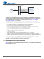
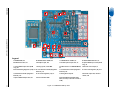
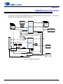
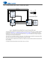
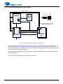
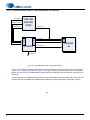
CDB48500 High-performance, 32-Bit Audio Decoder DSP Family CDB48500-USB USB Evaluation Kit Guide Copyright Cirrus Logic, Inc. 2014 (All Rights Reserved) http://www.cirrus.com DS784DB2 FEB '14 CDB48500 Contacting Cirrus Logic Support For all product questions and inquiries contact a Cirrus Logic Sales Representative. To find the one nearest to you go to www.cirrus.com IMPORTANT NOTICE “Preliminary” product information describes products that are in production, but for which full characterization data is not yet available. Cirrus Logic, Inc. and its subsidiaries (“Cirrus”) believe that the information contained in this document is accurate and reliable. However, the information is subject to change without notice and is provided “AS IS” without warranty of any kind (express or implied). Customers are advised to obtain the latest version of relevant information to verify, before placing orders, that information being relied on is current and complete. All products are sold subject to the terms and conditions of sale supplied at the time of order acknowledgment, including those pertaining to warranty, indemnification, and limitation of liability. No responsibility is assumed by Cirrus for the use of this information, including use of this information as the basis for manufacture or sale of any items, or for infringement of patents or other rights of third parties. This document is the property of Cirrus and by furnishing this information, Cirrus grants no license, express or implied under any patents, mask work rights, copyrights, trademarks, trade secrets or other intellectual property rights. Cirrus owns the copyrights associated with the information contained herein and gives consent for copies to be made of the information only for use within your organization with respect to Cirrus integrated circuits or other products of Cirrus. This consent does not extend to other copying such as copying for general distribution, advertising or promotional purposes, or for creating any work for resale. CERTAIN APPLICATIONS USING SEMICONDUCTOR PRODUCTS MAY INVOLVE POTENTIAL RISKS OF DEATH, PERSONAL INJURY, OR SEVERE PROPERTY OR ENVIRONMENTAL DAMAGE (“CRITICAL APPLICATIONS”). CIRRUS PRODUCTS ARE NOT DESIGNED, AUTHORIZED OR WARRANTED FOR USE IN PRODUCTS SURGICALLY IMPLANTED INTO THE BODY, AUTOMOTIVE SAFETY OR SECURITY DEVICES, LIFE SUPPORT PRODUCTS OR OTHER CRITICAL APPLICATIONS. INCLUSION OF CIRRUS PRODUCTS IN SUCH APPLICATIONS IS UNDERSTOOD TO BE FULLY AT THE CUSTOMER'S RISK AND CIRRUS DISCLAIMS AND MAKES NO WARRANTY, EXPRESS, STATUTORY OR IMPLIED, INCLUDING THE IMPLIED WARRANTIES OF MERCHANTABILITY AND FITNESS FOR PARTICULAR PURPOSE, WITH REGARD TO ANY CIRRUS PRODUCT THAT IS USED IN SUCH A MANNER. IF THE CUSTOMER OR CUSTOMER'S CUSTOMER USES OR PERMITS THE USE OF CIRRUS PRODUCTS IN CRITICAL APPLICATIONS, CUSTOMER AGREES, BY SUCH USE, TO FULLY INDEMNIFY CIRRUS, ITS OFFICERS, DIRECTORS, EMPLOYEES, DISTRIBUTORS AND OTHER AGENTS FROM ANY AND ALL LIABILITY, INCLUDING ATTORNEYS' FEES AND COSTS, THAT MAY RESULT FROM OR ARISE IN CONNECTION WITH THESE USES. Cirrus Logic, Cirrus, the Cirrus Logic logo designs, and DSP Composer are trademarks of Cirrus Logic, Inc. All other brand and product names in this document may be trademarks or service marks of their respective owners. DTS is a registered trademark of the Digital Theater Systems, Inc. DTS NEO:6 is a trademark of the Digital Theater Systems, Inc. It is hereby notified that a third-party license from DTS is necessary to distribute software of DTS in any finished end-user or ready-to-use final product. SRS, Circle Surround, and Trusurround are registered trademarks of SRS Labs, Inc. SRS Focus and Dialog Clarity are trademarks of SRS Labs, Inc. The CIRCLE SURROUND TECHNOLOGY rights incorporated in the Cirrus Logic chip are owned by SRS Labs, Inc. and by Valence Technology Ltd., and licensed to Cirrus Logic, Inc. Users of any Cirrus Logic chip containing enabled CIRCLE SURROUND TECHNOLOGY® (i.e., CIRCLE SURROUND® LICENSEES) must first sign a license to purchase production quantities for consumer electronics applications which may be granted upon submission of a preproduction sample to, and the satisfactory passing of performance verification tests performed by SRS Labs, Inc., or Valence Technology Ltd. E-mail requests for performance specifications and testing rate schedule may be made to [email protected]. SRS Labs, Inc. and Valence Technology, Ltd., reserve the right to decline a use license for any submission that does not pass performance specifications or is not in the consumer electronics classification. All equipment manufactured using any Cirrus Logic chip containing enabled CIRCLE SURROUND® TECHNOLOGY must carry the Circle Surround® logo on the front panel in a manner approved in writing by SRS Labs, Inc., or Valence Technology Ltd. If the Circle Surround® logo is printed in users manuals, service manuals or advertisements, it must appear in a form approved in writing by SRS Labs, Inc., or Valence Technology, Ltd. The rear panel of Circle Surround® products, users manuals, service manuals, and all advertising must all carry the legends as described in LICENSOR'S most current version of the CIRCLE SURROUND Trademark Usage Manual. Dolby, Dolby Digital, the double-D symbol, ProLogic, and Audistry are registered trademarks of Dolby Laboratories, Inc. Supply of an implementation of Dolby technology does not convey a license nor imply a right under any patent, or any other industrial or intellectual property right of Dolby Laboratories, to use the implementation in any finished enduser or ready-to-use final product. It is hereby notified that a license for such use is required from Dolby Laboratories. Intel is a registered trademark of Intel Corporation. Motorola is a registered trademark and SPI is a trademark of Motorola, Inc. I2C is a registered trademark of Philips Semiconductor Corp. Microsoft, Windows, and Windows XP are registered trademarks of Microsoft Corporation. ii CDB48500 USB Evaluation Kit Guide CDB48500 Contents Contents . . . . . . . . . . . . . . . . . . . . . . . . . . . . . . . . . . . . . . . . . . . . . . . . . . . . . . . . . . . . . . . . . . . . . . iii Figures . . . . . . . . . . . . . . . . . . . . . . . . . . . . . . . . . . . . . . . . . . . . . . . . . . . . . . . . . . . . . . . . . . . . . . . . . v Chapter 1. Introduction to the CRD48500-USB Evaluation Kit ......................... 1-1 1.1 CDB48500-USB Kit Contents and Requirements . . . . . . . . . . . . . . . . . . . . . . . . . . . . . . . . . 1-1 1.1.1 CDB48500-USB Kit ........................................................................................................ 1-1 1.1.2 PC Requirements ........................................................................................................... 1-1 1.1.3 Software Requirements.................................................................................................. 1-1 1.1.4 Support Hardware Requirements................................................................................... 1-1 1.1.5 Cabling Requirements.................................................................................................... 1-1 1.2 Introducing the CDB48500-USB Customer Development Kit . . . . . . . . . . . . . . . . . . . . . . . . 1-1 1.2.1 Identifying CDB48500-USB Components ...................................................................... 1-2 1.2.2 Related Documentation.................................................................................................. 1-4 1.2.2.1 Additional CDB48500 Evaluation Board Information..................................... 1-4 1.2.2.2 CS485xx Family DSP Hardware Information ................................................ 1-4 1.2.2.3 CS485xx Family DSP Software Information.................................................. 1-4 1.2.2.4 DSP Software Utility Information ................................................................... 1-4 1.2.2.5 Audio CODEC Information ............................................................................ 1-4 1.2.2.6 S/PDIF Receiver Information......................................................................... 1-4 Chapter 2. Board Setup and Installing the Evaluation Kit Software ................ 2-1 2.1 Introduction . . . . . . . . . . . . . . . . . . . . . . . . . . . . . . . . . . . . . . . . . . . . . . . . . . . . . . . . . . . . . . . . 2-1 2.1.1 Installing the Evaluation Kit Software ............................................................................. 2-1 2.1.2 Setting up the Evaluation Kit Boards.............................................................................. 2-3 2.1.3 Connecting to a PC ........................................................................................................ 2-4 2.1.4 Running a Stereo PCM Application on CDB48500-USB................................................ 2-6 2.1.5 Downloading Other Applications .................................................................................... 2-6 Chapter 3. CDB48500 System Description ......................................................... 3-1 3.1 CDB48500 System Block Descriptions. . . . . . . . . . . . . . . . . . . . . . . . . . . . . . . . . . . . . . . . . . 3-2 3.1.1 Audio Inputs ................................................................................................................... 3-2 3.1.1.1 Analog Line-level Inputs ................................................................................ 3-2 3.1.1.2 Digital Optical Input ....................................................................................... 3-2 3.1.1.3 Digital Coaxial Input....................................................................................... 3-2 3.1.1.4 Microphone Input........................................................................................... 3-2 3.1.2 Audio Outputs ................................................................................................................ 3-2 3.1.2.1 Analog Line-level Outputs ............................................................................. 3-2 3.1.2.2 Headphone Output ........................................................................................ 3-3 3.1.2.3 Optical Digital Output (PCM) ......................................................................... 3-3 3.1.3 DC Power Input .............................................................................................................. 3-3 3.1.4 Control Header ............................................................................................................... 3-3 3.1.5 On-Board Voltage Selection Headers ............................................................................ 3-3 3.1.6 Audio Input Source Multiplexer Selection Headers ........................................................ 3-4 3.1.7 Cirrus Logic CS485xx Audio DSP .................................................................................. 3-4 3.1.8 CS8416 S/PDIF RX........................................................................................................ 3-5 3.1.9 CS42448 Audio CODEC ................................................................................................ 3-5 3.1.10 Memory ........................................................................................................................ 3-5 3.1.11 Audio Clocking ............................................................................................................. 3-5 3.1.11.1 Clock and Data Flow for up to 8 Channel ADC inputs................................. 3-6 3.1.11.2 Clock and Data Flow for S/PDIF Input......................................................... 3-7 3.1.11.3 Clock and Data Flow for CDB USB Master Card Source ............................ 3-8 CDB48500 USB Evaluation Kit Guide iii CDB48500 Chapter 4. Configuring the CDB48500 ................................................................ 4-1 4.1 Introduction . . . . . . . . . . . . . . . . . . . . . . . . . . . . . . . . . . . . . . . . . . . . . . . . . . . . . . . . . . . . . . . . 4-1 4.2 Basic Application Download and System Configuration for PCM Pass-through. . . . . . . . 4-1 4.2.1 System Block ................................................................................................................. 4-2 4.2.2 Changing the Audio Input Source .................................................................................. 4-3 4.2.2.1 Audio In via S/PDIF ....................................................................................... 4-3 4.2.2.2 Audio In via 8-channel ADC .......................................................................... 4-3 4.2.2.3 Audio In via USB ........................................................................................... 4-4 4.2.2.4 DAI Input of CS485xx .................................................................................... 4-4 4.2.3 Changing Audio Output Configuration............................................................................ 4-5 4.2.3.1 DAO Output of CS485xx ............................................................................... 4-5 4.2.3.2 CS42448 DAC Properties.............................................................................. 4-6 4.2.4 Changing Serial Control Protocol (I2C or SPI) ............................................................... 4-7 4.2.5 Headphone Output ......................................................................................................... 4-8 4.2.6 S/PDIF Transmitter......................................................................................................... 4-9 Appendix A. Schematics .....................................................................................A-1 A.1 Introduction . . . . . . . . . . . . . . . . . . . . . . . . . . . . . . . . . . . . . . . . . . . . . . . . . . . . . . . . . . . . . . . A-1 A.1.1 Schematic Pages ...........................................................................................................A-1 A.1.1.1 Detailed Schematic Descriptions ..................................................................A-1 A.1.1.1.1 CS48500 System Block Diagram (See Figure A-1) ........................A-1 A.1.1.1.2 DSP Input Data Multiplexing (See Figure A-2)................................A-1 A.1.1.1.3 Coyote DSP Core (See Figure A-3) ................................................A-1 A.1.1.1.4 Serial Flash Memory (See Figure A-4) ...........................................A-2 A.1.1.1.5 S/PDIF Receiver (See Figure A-5)..................................................A-2 A.1.1.1.6 Codec #1(CS42448) (See Figure A-6)............................................A-3 A.1.1.1.7 Codec #2 (CS42448) (See Figure A-7)...........................................A-3 A.1.1.1.8 Codec 1 and Codec 2 Input Filters (See Figure A-8) ......................A-4 A.1.1.1.9 Output Filters & Headphone Output (See Figure A-9) ....................A-4 A.1.1.1.10 Mic and Pre-Amp (See Figure A-10).............................................A-4 A.1.1.1.11 Control Connector and Power (See Figure A-11) .........................A-4 Appendix B. Troubleshooting Guide..................................................................B-1 B.1 Intoduction . . . . . . . . . . . . . . . . . . . . . . . . . . . . . . . . . . . . . . . . . . . . . . . . . . . . . . . . . . . . . . . . B-1 B.1.1 Solutions to Possible Problems .....................................................................................B-1 B.1.1.1 Power LEDs are Not illuminated ...................................................................B-1 B.1.1.2 CDB48500 is Not Recognized by the PC......................................................B-1 B.1.1.3 Unable to Run a Stereo PCM Application .....................................................B-1 Revision History....................................................................................................B-2 iv CDB48500 USB Evaluation Kit Guide CDB48500 Figures Figure 1-1. CDB48500-USB System Block Diagram ......................................................................................... 1-2 Figure 1-2. CDB48500-USB Top View ............................................................................................................... 1-3 Figure 2-1. CDB USB MASTER Driver Setup .................................................................................................... 2-2 Figure 2-2. Board Setup Diagram ...................................................................................................................... 2-3 Figure 2-3. Found New Hardware Service Window ........................................................................................... 2-4 Figure 2-4. Found New Hardware Wizard Welcome Window ............................................................................ 2-4 Figure 2-5. Found New Hardware Wizard Finish Window ................................................................................. 2-5 Figure 2-6. Microsoft Windows XP Windows ................................................................................................... 2-5 Figure 3-1. CDB48500 Block Diagram ............................................................................................................... 3-1 Figure 3-2. Simplified Clock and Data Flow for up to 8 Channel ADC Inputs .................................................... 3-6 Figure 3-3. Simplified Clock and Data Flow for S/PDIF Input ............................................................................ 3-7 Figure 3-4. CDB USB Master Card Clocking and Data Flow ............................................................................. 3-8 Figure 4-1. PCM Pass-through Example Application ......................................................................................... 4-2 Figure 4-2. System Configuration ...................................................................................................................... 4-2 Figure 4-3. Audio In via S/PDIF In ..................................................................................................................... 4-3 Figure 4-4. Audio In via 8 Channel ADC ............................................................................................................ 4-4 Figure 4-5. DAI Device Properties ..................................................................................................................... 4-5 Figure 4-6. CDB48500 Digital Audio Output Properties ..................................................................................... 4-6 Figure 4-7. Codec DAC Properties .................................................................................................................... 4-7 Figure 4-8. CDB48500 Comm Mode .................................................................................................................. 4-8 Figure 4-9. Remap Tab ...................................................................................................................................... 4-8 Figure A-1. CS48500 System Block Diagram .................................................................................................... A-6 Figure A-2. DSP Input Data Multiplexing Schematic........................................................................................... A-7 Figure A-3. DSP Schematic ................................................................................................................................ A-8 Figure A-4. Serial Flash Memory Schematic....................................................................................................... A-9 Figure A-5. SPDIF Receiver Schematic............................................................................................................ A-10 Figure A-6. Codec #1(CS42448) Schematic..................................................................................................... A-11 Figure A-7. Codec #2 (CS42448) Schematic.................................................................................................... A-12 Figure A-8. Codec 1 and Codec 2 Input Filters Schematic ............................................................................... A-13 Figure A-9. Output Filters & Headphone Output .............................................................................................. A-14 Figure A-10. Mic Preamp Schematic ................................................................................................................ A-15 Figure A-11. Control Connector and Power Schematic .................................................................................... A-16 CDB48500 USB Evaluation Kit Guide v Chapter 1 Introduction to the CRD48500-USB Evaluation Kit 1.1 CDB48500-USB Kit Contents and Requirements 1.1.1 CDB48500-USB Kit Each CDB48500-USB kit comes with the following: • CDB48500 Development Board (See Figure 1-2) • Power Supply: +9V, 1.67A, 100V - 240V, with AC Power Cord • CDB USB MASTER Digital I/O Card (See Figure 1-2) • USB Cable • 3 Board Overlays Identifying the Outputs for CS48520, CS48540, and CS48560 • Document Card Explaining How to Get the Latest Board Software 1.1.2 PC Requirements • Microsoft Windows XP® or Windows 7® Operating System • USB 2.0 Support 1.1.3 Software Requirements • Cirrus Evaluation Software Package (available from your local Cirrus Logic representative) 1.1.4 Support Hardware Requirements • Digital or Analog Audio Source (e.g. DVD player, PC with a digital audio card/device) • Amplified Speakers for audio playback (e.g. powered PC speakers, AVR/amp + speakers) 1.1.5 Cabling Requirements • Digital Audio Inputs – S/PDIF Optical or Coaxial RCA Cables (Connect to digital audio card, audio analyzer, or DVD player.) • Digital Audio Output – S/PDIF Optical Cable (Connect to digital audio card, audio analyzer, or AVR.) • Analog Audio Inputs – RCA Audio Cables (Connect CDB48500 line-level inputs to analog audio source.) • Analog Audio Outputs – RCA Audio Cables (Connect CDB48500 line-level outputs to powered speakers.) 1.2 Introducing the CDB48500-USB Customer Development Kit The CDB48500-USB kit is composed of the CDB48500 customer development board and the CDB USB MASTER Control board. The CDB48500 provides a practical platform for emulating a typical multi-channel audio system application. The CDB USB MASTER is a USB control board used to interface the host PC to the CDB48500 board, and convert GUI commands into the serial control protocol required for configuring the CS485XX DSP, (2)CS42448 codecs, and CS8416 S/PDIF receiver ICs. Figure 1-1 shows the relationship 1 PC USB Port CDB USB MASTER between the PC, CS485XX, and the CDB USB MASTER Serial Control Interface Reset Signals Board Control Signals CDB48500 Audio Data (Future Development) Figure 1-1. CDB48500-USB System Block Diagram This document will concentrate on the features and basic operation of the CDB48500-USB board. Detailed information regarding the operation and programming of the CS485XX DSP is covered by the CS485XX data sheet, CS485XX Hardware User’s Manual, and application note AN298 (see Section 1.2.2, “Related Documentation” on page 1-4 for more details). The CDB48500-USB is a convenient and easy-to-operate evaluation platform. It has been designed to demonstrate the majority of the CS485XX functions on a small 6" x 6.5" base board. These features include: • PC control of the CS485XX using the DSP Composer™ graphical user interface • Serial control of audio devices on CDB48500 via I2C® or SPI™ protocols • Digital audio input of PCM via optical or coaxial S/PDIF (does not support compressed data input) • Up to 12-channel analog audio input via the two CS42448 audio codecs • Up to 12-channel analog output through the two CS42448 audio codecs • Digital audio output of PCM data via optical S/PDIF • Headphone output jack • Multi-channel digital audio input via the CDB USB MASTER card (not yet supported) • Separate input and output clocking domains to allow 1FS-to-2FS audio processing on the CS485XX • Fast boot – host-controlled master boot (HCMB) of custom applications from 4 Mbit serial SPI flash device. • Microphone input with integrated amplifier for Intelligent Room Calibration (IRC) evaluation (future) • Supports all members of the CS485XX family in the 48-pin LQFP package. Note: Not all features of the CS485xx are exercised on the CDB48500. 1.2.1 Identifying CDB48500-USB Components Figure 1-2 shows the top side of the CDB48500-USB Evaluation Board. The accompanying legend identifies the main components of the board. 2 DS784DB2 Copyright 2014 Cirrus Logic Legend: A.CS485XX DSP, U6 B.CS42448 Audio CODEC, U4 C.CS42448 Audio CODEC, U5 D.CS8416 S/PDIF Receiver, U3 E.4 Mbit Serial Flash, U11 F.Headphone jack, J20 G.1/8” Microphone Input Jack, J5 H.Optical S/PDIF Input Jacks (PCM only), J2 I. Coaxial S/PDIF Input Jacks (PCM only), J31 J.Analog Inputs, 2 Vrms Max K.USB Connector on CDB USB Master, L.Alternate +12V Jumper, J3 P1 M.+3.3V Switching Regulator (1.5A), U8 N.+3.3V Selection Header (Regulator/ External), J17 O.+1.8V Selection Header (Regulator/ External), J18 P.+1.8V Linear Regulator (1A), U14 Q.+5V Selection Header (Regulator/ External), J19 R.+5V Linear Regulator (1A), U7 S.Analog Audio Outputs T.DC Power Input Jack, +9Vdc to +12Vdc, J25 U.Optical S/PDIF Output Jack, J24 V.Power Indicator LEDs W.On-board/External Digital Audio Mux, U1 & U2 (U1 & U2 are on back of PCB.) 1-3 Figure 1-2. CDB48500-USB Top View 1.2.2 Related Documentation The documents described in this section are updated periodically and may be more up-to-date than the information in this document. Check the Cirrus Logic Internet site for the latest updates. 1.2.2.1 Additional CDB48500 Evaluation Board Information The following information about the CDB48500 Evaluation Board can be obtained from your Cirrus Logic representative: • Schematics • BOM • Artwork and PCB stackup 1.2.2.2 CS485xx Family DSP Hardware Information The following documents are installed with the CS485xx System Development Kit (SDK). • CS485xx Family Data Sheet • CS485xx Hardware Users Manual • CS485xx Errata 1.2.2.3 CS485xx Family DSP Software Information The following document is installed with the CS485xx SDK: • AN298, CS485xx Firmware User’s Manual 1.2.2.4 DSP Software Utility Information The following document is installed with the CS485xx SDK: • DSP Composer User’s Manual The documents listed above are updated periodically and may be more up to date than the information in this document. Check the Cirrus Logic Internet site for the latest updates. 1.2.2.5 Audio CODEC Information The following information is located on the www.cirrus.com Internet site: • CS42448 Data Sheet • CS42448 Errata 1.2.2.6 S/PDIF Receiver Information The following information is located on the www.cirrus.com Internet site: • CS8416 Data Sheet • CS8416 Errata §§1 1. The “§§” symbol is used throughout this manual to indicate the end of the text flow in a chapter. 4 Chapter 2 Board Setup and Installing the Evaluation Kit Software 2.1 Introduction It is important to install the Evaluation Software BEFORE connecting the USB cable from the PC to the CDB USB MASTER card. Failure to install the evaluation software before the initial connection can result in an inability to communicate with the CBD485xx. 2.1.1 Installing the Evaluation Kit Software The DSP evaluation software installation will first install the Cirrus Logic DSP evaluation software followed by the USB drivers required to communicate with the CDB USB MASTER. 1. Run the latest DSP evaluation software installation executable (CS485xx_eval_kit_rc<revision number>.exe ). This executable is supplied by your Cirrus Logic representative. 2. At the Welcome screen, click Next. 3. At the Licensing Agreement window, select the “I accept the agreement” radio button to agree to the terms and then select Next. 4. Select the Destination Location window, Select the default location “C:\CirrusDSP” and click Next. 5. Select Start Menu Folder window, Select the default location “C:\CirrusDSP” and click Next. 6. The Ready to Install window indicates the selected destination location and the Start menu folder for confirmation, select Install to begin the install process which should take less than one minute. 7. After the DSP evaluation software is installed, the installer will launch the Front Panel Driver Setup Wizard (below). Click Next to continue the installation. Figure 2-1. CDB USB MASTER Driver Setup 1 8. The Opal Kelly Licensing Agreement window will appear next. Click “I Agree” to agree to the terms and continue. 9. The next window asks the user to choose components for installation. By default, only one component is available and is pre-selected – Unified USB Driver. Click Next to continue. 10. The wizard will then ask the user to choose the install location. Select the default location of “C:\Program Files\Opal Kelly\FrontPanel” and click Install. This should take only a few seconds. 11. Click Finish once the wizard has completed installation of the drivers. 12. The Cirrus DSP evaluation software will then prompt the user to click Finish to exit the Setup wizard. MIC_IN 2.1.2 Setting up the Evaluation Kit Boards Optical Output on DVD Player CDB48540 UNUSED UNUSED AIN_4B AIN_4A UNUSED UNUSED DVD P layer Optical Cable AIN_3A AIN_3B AIN_2A AIN_2B AIN_1B AIN_1A AIN_1B AOUT_6B AOUT_5B AOUT_4B AOUT_3B AOUT_2B AOUT_1B AOUT_6A UNUSED AOUT_4B UNUSED AOUT_4A UNUSED AIN_2B UNUSED UNUSED UNUSED UNUSED UNUSED UNUSED AIN_1B UNUSED UNUSED UNUSED AOUT_2B UNUSED UNUSED UNUSED AOUT_2A UNUSED To Powered Speakers AOUT_1B RCA Cables AIN_2A HP_OUT Analog Outputs Optical Output UNUSED UNUSED AIN_1A “A” Power Cable CDB48520 UNUSED AOUT_5A AOUT_4A AOUT_3A AOUT_1A AOUT_2A SPDIF_TX PWR +9V USB Cable UNUSED AOUT_3B AIN_2B AOUT_3A AIN_2A Analog Inputs AOUT_2B AIN_3B AOUT_1B AIN_3A AOUT_2A AIN_4B AOUT_1A USB 2.0 Port AIN_5B AIN_4A HP_OUT “B” rru s So Log ftw i are c AIN_6A AIN_5A AIN_1A U S B Ci AIN_6B MIC_IN CS48560 CDB48560 AOUT_1A MIC_IN SPDIF_RXIN SPDIF_RXP HP_OUT Figure 2-2. Board Setup Diagram 1. Place the CDB48500 and the CDB USB MASTER on a static-free surface. 2. If the boards are not mated, connect them together as shown in Fig. 2-2. Notice that the USB connector on the CDB USB MASTER and the power connector on the CDB48500 are on the same side. 3. Connect the Power Supply as follows: A. Connect the power supply jack to the CDB48500 board at J25 and the adapter to a wall power socket or power strip. B. Check that the D3 (green, 3.3V), D2 (red, 1.8V), and D4 (orange, 5V) power indicator LEDs illuminate on the CDB48500. 4. Setup Audio Input connections to the CDB48500 as follows: A. Connect one end of the digital audio S/PDIF optical cable to SPDIF_RXP on the CDB48500 board. 2 B. Connect the other end of the optical cable to the optical output on the back of a DVD player or other digital audio source. 5. Setup Audio Output connections from CDB48500 as follows: A. The RCA connectors labeled AOUT_1A and AOUT_1B are the left and right analog output channels. B. Use the RCA audio cables to connect these line-level analog outputs to powered speakers. 2.1.3 Connecting to a PC Follow these steps to connect to a PC: 1. Connect the “B” end of the USB cable to P1 on the CDB USB MASTER USB Digital I/O Card. 2. Connect the “A” end of the USB Cable to a USB 2.0 port on a notebook or PC running Win XP. 3. Windows should recognize that a new device has been attached and display a notice saying “Found New Hardware”. Figure 2-3. Found New Hardware Service Window 4. Windows will display the Found New Hardware Wizard (below). Select the No, not at this time radio button so that Windows does not connect to Windows Update for the drivers. Click Next. Figure 2-4. Found New Hardware Wizard Welcome Window 5. Windows will then ask whether to use automatic installation or manual installation. Allow Windows to install the software automatically and click Next. 3 Figure 2-5. Found New Hardware Wizard Finish Window 6. It is possible that during the installation, Windows might issue a warning that the drivers have not passed “Windows Logo” testing. Select Continue Anyway. Figure 2-6. Microsoft Windows XP Message Screen 7. Windows should now locate the correct drivers and complete the installation. 4 2.1.4 Running a Stereo PCM Application on CDB48500-USB To run a stereo PCM application, follow these steps: 1. Launch DSP composer (Start Program Cirrus Logic DSP CS485XXDSP Composer). 2. In DSP Composer, go to File Open and open the appropriate project. 3. Press the GO button 4. Insert PCM material into the DVD player (e.g., music CD). If a DVD is being used as the audio source, make sure that the DVD Player (or other digital audio source) is configured to output PCM data. 5. Press Play on the DVD player (or other digital audio source). You should now hear audio from the speakers. 2.1.5 Downloading Other Applications Separate project files (.cpa) are provided for other applications such as Dolby® Pro Logic® II, DTS Neo6™, Audistry® by Dolby®, SRS® Circle Surround®. In order to evaluate these, please contact your local FAE to ensure the necessary licensing agreements have been completed. Please note that the CDB48500-USB does not support multi-channel decoding such as Dolby Digital® or DTS® because the CS485XX DSP is only a post-processor and does not contain a decoder. §§ 5 Chapter 3 CDB48500 System Description A detailed block diagram of the CDB48500 Customer Development Board is shown in Figure 3-1. The sections that follow provide a detailed description of each block. MIC Preamp Analog Analog Analog Analog Up to 12 Analog In In In Analog In In Inputs Analog Analog Analog Analog Up to 12 Analog In In Analog In In In Outputs MIC In 2x CS42448 CS42448 Headphone Out ADC Data CS42448_RESET Audio Clocks 0 1 DAO Audio Out USB Clocks/Data SPI / I2C CS485XX SPI FLASH WDO I2C FLASH LED SPDIF OUT DAO[3] S/PDIF Out DSP_RESET DAO Audio Out XTAL_OUT Control Header – J11 S/PDIF Data CS8416 SPDIF IN BRD_RESET S/PDIF In Figure 3-1. CDB48500 Block Diagram 1 3.1 CDB48500 System Block Descriptions 3.1.1 Audio Inputs 3.1.1.1 Analog Line-level Inputs • Connector Type: RCA Female • Absolute Maximum Signal Level: +6.5V • Absolute Minimum Signal Level: GND - 0.7V • Full Scale Amplitude: 2VRMS • Reference Designators: J4, J6-J10, J12, J26-J30, or AIN1A - AIN6B 3.1.1.2 Digital Optical Input Note: Digital Optical Input is PCM only as there is no multi-channel decoder present on CDB48500-USB. • Connector Type: Fiber Optic RX for Digital Audio, JIS F05 (JIS C5974-1993 F05) • Reference Designator: J2, or SPDIF_RXP 3.1.1.3 Digital Coaxial Input Note: Digital Coaxial Input is PCM only as there is no multi-channel decoder present on CDB48500-USB. • Connector Type: RCA Female • Maximum Signal Level: +3.3V • Minimum Signal Level: GND - 0.7V • Reference Designator: J31, or SPDIF_RXN 3.1.1.4 Microphone Input • Absolute Maximum Signal Level: +5V • Absolute Minimum Signal Level: GND - 0.7V • Full Scale Amplitude: 7mVp-p • Reference Designator: J5 The microphone preamplifier shares the AIN1_5 ADC with the AIN3_A RCA jack. Only one analog source can be sampled at any given time. When the microphone input is selected, the AIN3_A audio jack is ignored. The default configuration enables the AIN3_A audio jack. 3.1.2 Audio Outputs 3.1.2.1 Analog Line-level Outputs • Connector Type: RCA Female • Full Scale Amplitude: 1.21VRMS • Reference Designators: J13-J16, J33-J40, or AOUT_1A - AOUT_6B 3.1.2.2 Headphone Output 2 • Connector Type: 1/8” TRS Female • Full Scale Amplitude: 3.53 VRMS • Reference Designator: J20, or HP_OUT 3.1.2.3 Optical Digital Output (PCM) • Connector Type: Fiber Optic TX for Digital Audio, JIS F05 (JIS C5974-1993 F05) • Reference Designator: J24, or SPDIF_TX The S/PDIF output uses the same data line as AOUT_4A and AOUT_4B. When the digital output has been enabled, and you have speakers connected to AOUT_4A and AOUT_4B white noise will be heard. This could damage the speakers. 3.1.3 DC Power Input • Voltage Range: +9VDC TO +12VDC • Minimum Power: 8W supply • Connector Type: 2mm Female, positive center pin • Reference Designator: J25 3.1.4 Control Header • Connector Type: 2x25, 0.100 inch Shrouded Male • Reference Designator: J11 This connector is the interface between the CDB48500 and the CDB USB MASTER. Control signals, clocks, data, and +3.3V power are passed across this connector. 3.1.5 On-Board Voltage Selection Headers • Connector Type: 1x3, 0.100 inch, Stake Header • Reference Designator: J17 - J19 The CDB48500-USB is designed to operate from a single DC power input. The 9V power supply provided with the kit is connected to the DC power input jack (J25) and is regulated down to the system voltages (5V, 3.3V, 1.8V). The power selection headers should be set to the ‘REG’ position when using the DC wall supply. This is the default mode of operation and should not need to be changed for most applications. It is possible to bypass the regulated power supplies for any of the voltages by removing the jumper from the appropriate power selection header, and connecting an external voltage supply to the center pin of that selection header. The third configuration for the power selection headers is the ‘EXT’ position. This is a special mode of operation, and cannot be used while connected to the CDB USB MASTER control board. Placing the power selection headers in the ‘EXT’ position while connected to the CDB USB MASTER will prevent the board from operating. The unpopulated header, J3, is also designed for a special mode that brings 12V from the control header, but cannot be used when connected to the CDB USB MASTER. 3 3.1.6 Audio Input Source Multiplexer Selection Headers The CDB48500-USB includes jumpers to change DSP DAI inputs. • Source 0: CDB USB MASTER Board, controlled from Software (Refer to Section 4.2.2, “Changing the Audio Input Source” on page 4-3) • Source 1: 2 Channels from CS8416 and 8 channels from (2)CS42448, short pins 2 and 3 of J100 • Source 2: 12 Channels from (2)CS42448 codecs, short pins 1 and 2 of J100 • Reference Designators: U1, U2, U9, U18, and J100 These multiplexers are used to select which audio sources feed the CS485XX DAI pins. When the on-board sources (CS8416, U3 and CS42448, U4 and U5) are being used, the CDB USB MASTER data cannot be processed. The CDB48500 contains a header to connect DAI pins, DAO pins, and clocks to external circuitry. The DAO and clock pins are • DAI[5,3:0] feed from J102 header, short pins 1 and 3 on J101 • DAI[5,3:0] feed from on board sources, short pins 3 and 5 on J101 • DAI[4] feed from J102 header, short pins 2 and 4 on J101 • DAI[4] feed from on board sources, short pins 4 and 6 on J101 • The DAO pins and clocks are paralleled to both the on board devices and J102, J103 headers 3.1.7 Cirrus Logic CS485xx Audio DSP The CS485xx audio DSP (U6) are a family of 32-bit fixed point processors designed specifically for audio applications. The CDB48500 allows a designer to evaluate the CS485xx DSPs in many different modes of multi-channel input and output. The 48-pin footprint on this board is compatible with any CS485XX chip. Audio input data to the DSP can come from any of the following sources: • CS8416 (U3) • CS42448 (U4 and U5) • CDB USB MASTER card • Header for external codecs (not yet supported) Audio output data from the DSP can be sent to the following destinations: • Both CS42448’s for conversion to Analog Output (AOUT_1A - AOUT_6B) • Optical S/PDIF Out (SPDIF_TX), this option disables AOUT_4A and AOUT_4B • CDB USB MASTER card The CS485XX has many applications stored in internal ROM, but a host is still required to configure the application for a particular system. The CDB48500-USB allows the PC to act as a host to boot and configure the DSP through the GUI software. The CS485XX can also be booted from external serial flash for custom applications that are not stored in the DSP’s ROM. Note: The 48-pin footprint on this board is also compatible with the CS485XX family of DSPs. The CDB48500 can support any CS485XX chip if the alternate stuffing options shown on the DSP schematic page have been followed. 4 3.1.8 CS8416 S/PDIF RX The CS8416 (U3) is a 192 kHz S/PDIF receiver with an integrated input multiplexer. The two S/PDIF input jacks (RXP-RXN) are connected to the CS8416. Only one of the optical or coaxial S/PDIF jacks can be used at a time and is automatically selected by the CS8416. When S/PDIF audio is being processed, the CS8416 must master MCLK for the system (see "Audio Clocking" on page 1-5 for details). 3.1.9 CS42448 Audio CODEC The CS42448 (U4 and U5) is a high-performance, multi-channel audio CODEC capable of supporting sample rates up to 192 kHz on its 6ADCs and 8 DACs. There are two of these devices on the CDB48500 and are used for all analog-to-digital and digital-to-analog conversions. All analog inputs (AIN_1A-AIN_6B) and all analog outputs (AOUT_1A-AOUT_6B) are connected to the CS42448s. The microphone input shares the AIN1_5 ADC with the AIN_3A RCA jack. When the microphone is in use, the AIN_3A RCA jack is ignored. When analog audio is being processed, the 24.576 MHz crystal for the CS485XX must master MCLK for the system (see Section 3.1.11. for details). 3.1.10 Memory The CDB48500 is populated with two 4 Mbit SPI flash devices and one I2C EEPROM. Selection from SPI to I2C is changed in Software. There are 2 SPI flash footprints (U11, U13) on the board for compatibility with both standard 8-pin serial flash pinouts. The serial control lines are shared by both footprints, and a chip select 0 ohm jumper resistor (R101) is populated to make U13 the active device. To make U11 the active device remove R101 and populate R110 with a 0 ohm resistor. There is also a jumper (J105) to select Program or Normal (Run) operation of the SPI flash devices. In program mode the CDB USB MASTER card will use the DSP_CS line to control the flash while holding the DSP in reset with the DSP_RST line. For program mode jumper pins 2 and 3 on J105. In normal the DSP controls the SPI device. In I2C mode no jumper change is required for program or normal mode of EEPROM. For normal mode jumper pins 1 and 2. The feature to program flash from the CDB USB MASTER is not yet supported. 3.1.11 Audio Clocking Clocking architecture is one of the most important aspects of a digital audio system. The input and output clock domains of the DSP must be synchronous when delivering audio data in an isochronous fashion (constant bitrate delivery), even if the input/output domains operate at different frequencies (e.g. 48 kHz input/96 kHz output). The CDB48500 can operate in three different clocking modes. Each of these modes is explained in the following sections. 5 3.1.11.1 Clock and Data Flow for up to 8 Channel ADC inputs MUXED_DAI[3:0] MUXED_DSP_LRCLK1 J101 \ON_BRD1 HDR1 MUXED_MCLK \ON_BRD2 HDR2 \SPDIF J100 CS8416 12CH_ADC MUXED_DSP_SCLK1 XTAL_OUT Use these jumper settings for the clocking mode and inputs shown in diagram. SDOUT DAI DAO DSP_SCLK DSP_LRCLK CS485XX DSP_DA0[3:0] SDIN CS42448 CS42448 2x 2x 8 Analog Inputs XMTA S/PDIF OUT Figure 3-2. Simplified Clock and Data Flow for up to 8 Channel ADC Inputs The ADC clocking architecture is used when the ADCs are used as the only audio input (i.e. S/PDIF is disabled as described in Section 4.2.2, “Changing the Audio Input Source” on page 4-3), and the audio input source multiplexer (U1, U2) is used to select on-board audio sources. Figure 3-2 illustrates this clocking configuration. The jumpers must be set as described above. XTAL_OUT from the CS485xx is MCLK for the system. The CS8416 slaves to this MCLK and generates SCLK and LRCLK for the ADC side of the CS42448 and the DAI side of the DSP. On the output side, the CS485xx slaves to MCLK from CS8416 and masters SCLK and LRCLK for the DAC side of the CS42448. An example of this clocking scheme can be found in pcm_mc_1fs.cpa. 6 3.1.11.2 Clock and Data Flow for S/PDIF Input MUXED_DSP_LRCLK1 J101 MUXED_MCLK \ON_BRD1 HDR1 PLL Use these jumper settings for the clocking mode and inputs shown in diagram. XTAL_OUT DSP_DAI4 HDR2 \SPDIF SPDIF Input J100 S/PDIF Input 12CH_ADC CS8416 \ON_BRD2 MUXED_DSP_SCLK1 SDOUT DAI DAO DSP_SCLK SDIN DSP_LRCLK DSP_DA0[3:0] CS485XX CS42448 CS42448 2x 2x XMTA SPDIF OUT Figure 3-3. Simplified Clock and Data Flow for S/PDIF Input Figure 3-3 illustrates the S/PDIF clocking architecture used when any S/PDIF RX is used as an audio source, as described in Section 4.2.2, “Changing the Audio Input Source” on page 4-3). MCLK recovered from the incoming S/PDIF stream is the MCLK for the system. The CS8416 also generates SCLK and LRCLK for the DAI side of the DSP from the recovered MCLK. On the output side, the CS485XX slaves to MCLK from CS8416 and masters SCLK and LRCLK for the DAC side of the CS42448. An example of this clocking scheme can be found in pcm.cpa. 7 3.1.11.3 Clock and Data Flow for CDB USB Master Card Source MUXED_DAI[4:0] MUXED_DSP_LRCLK1 MUXED_DSP_SCLK1 CDB USB MASTER CARD DAI DAO CS485XX MUXED_MCLK DSP_SCLK DSP_LRCLK SDIN CS42448 CS42448 2x 2x DSP_DA01[3:0] XMTA SPDIF OUT Figure 3-4. CDB USB Master Card Clocking and Data Flow Figure 3-4 illustrates the clocking architecture used when IIS(USB) is used as an audio source, as described in Section 4.2.2, “Changing the Audio Input Source” on page 4-3). MCLK is generated by the PLL on the USB Master card. The PLD on the USB Master Card generates SCLK and LRCLK for the DAI side of the DSP from the MCLK. On the output side, the CS485xx slaves to MCLK from the USB Master Card and masters SCLK and LRCLK for the DAC side of the CS42448.The CS485XX always masters its output clocks (DSP_SCLK/DSP_LRCLK). §§ 8 Chapter 4 Configuring the CDB48500 4.1 Introduction The DSP Composer™ software is a graphical user interface (GUI) that is used to program the CS485XX DSP, and to configure the CDB48500. With the exception of the power selection and DAI input jumpers, the CDB48500 is configured exclusively through software. This section provides basic instruction for using the GUI to control the CDB48500, but detailed information can be found in the DSP Composer™ User’s Manual. Both the DSP Composer™ software, and the User’s Manual for the software package will be provided by your local Cirrus Logic representative. 4.2 Basic Application Download and System Configuration for PCM Pass-through Follow the instructions in Chapter 1, "Board Setup and Installing the Evaluation Kit Software" in order to install the USB drivers on your PC and launch DSP Composer (the GUI used to control the CDB48500). After following the instructions in Section 2.1.4, “Running a Stereo PCM Application on CDB48500-USB” on page 1-5, the DSP Composer main window will appear as shown in Fig. 4-1. Fig. 4-1 shows the DSP Composer™ main window for a PCM pass-through application on the CDB48500. The blocks shown in the main window of DSP Composer™ can be selected from the folders in the left-hand window pane, and then connected together by “wires” to indicate the processing path as shown. The “Audio In” and “Audio Out” blocks represent the hardware ports that need to be configured. The “Audio In” block is used to select the S/PDIF Input, Analog input or USB input that is to be processed. It configures the digital audio format for the CS8416, ADC side of CS42448 and the DAI port of the CS485XX. The “Audio Out” block is used to configure the digital audio format for the DAC side of the CS42448, the DAO port of the CS485XX and enables or disables the S/PDIF TX output port of the CS485XX. Figure 4-1. PCM Pass-through Example Application 1 4.2.1 System Block The CDB48500 board is populated with a CS48560. However it is possible to evaluate the CS48520, CS48540, CS48560, CS485AU2B, and CS485DV2B on this board. When you drag the system block on to the work space, a popup menu is displayed as shown in Fig. 4-2. This menu lets you choose the target chip that you need to evaluate. When you select the target chip, place the template of the target chip on the analog connectors. The template is a guide that shows which input/output channels are valid for the selected chip. . Figure 4-2. System Configuration 4.2.2 Changing the Audio Input Source The audio input to the DSP is selected through the “Audio In” block in DSP Composer. The Audio can be delivered to the DSP via the following: • S/PDIF (J100 on S/PDIF) • Analog (J100 on 12CH_ADC) • Analog (J100 on 8CH_ADC) • Analog (J100 on 2CH_ADC) • USB (IIS) • Echo Audio 4.2.2.1 Audio In via S/PDIF To deliver data to the DSP via S/PDIF, drag the Audio In block to the work space and select “SPDIF” as the Input Source. Double click the Audio In block to see the signal flow. Right Click on SPDIF Rx. The device properties of the S/PDIF IN element lets you select if the SPDIF input is on SPDIF_RXP (Optical In) or on SPDIF_RXN (Coaxial). The Input FS depends on input stream and must not be changed. The Master/Slave property must always be set to Master to indicate that the S/PDIF transmitter masters MCLK, SCLK and LRCLK as described in Section 3.1.11.2, “Clock and Data Flow for S/PDIF Input” on page 1-7. The Audio In module with S/PDIF In as the input source is shown in Fig. 4-3. 2 Figure 4-3. Audio In via S/PDIF In 4.2.2.2 Audio In via 8-channel ADC To deliver data to the DSP via 8ch ADC, drag the Audio In block to the work space and select “Analog (8 ch)” as the Input Source. Double click the Audio In block to see the signal flow. The device properties of the Analog (8 ch) element lets you select if the sampling frequency of the ADC on the CS42448 CODEC. The Master/Slave property must always be set to Master to indicate that the ADC will master SCLK and LRCLK as described in Section 3.1.11.1, “Clock and Data Flow for up to 8 Channel ADC inputs” on page 1-6. The Audio In module with Analog (8-channel) as the input source is shown in Fig. 4-4. Figure 4-4. Audio In via 8 Channel ADC 4.2.2.3 Audio In via USB This feature is currently not supported. 3 4.2.2.4 DAI Input of CS485xx Each of the Audio In Elements listed above are connected to a DAI element. This represent the DAI port of the DSP. As shown in Fig. 4-5. This dialog allows the user to set the following parameters for the CS485xx: • SCLK Polarity • LRCLK Polarity • Reference Clock - Set to the frequency of the crystal driving the CS485XX(Y1). This is the reference clock is used to determine the clock dividers needed to derive Fs in ADC-only applications. If this number changes, then all dividers for LRCLK/SCLK will change by the same ratio (e.g., @24.576 MHz MCLK/512 = 1Fs = LRCLK, @12.288 MHz MCLK/256 = 1Fs = LRCLK. . Figure 4-5. DAI Device Properties 4.2.3 Changing Audio Output Configuration The audio output section of the CDB48500 is configured through the “Audio Out” block in DSP Composer. 4.2.3.1 DAO Output of CS485xx The digital audio output (DAO) of the CS485XX is very flexible, making it compatible with a wide variety of audio devices. This port can configured using the dialog box shown in Fig. 4-6. Right-click on the “Audio Out” block, then select Device Properties. Right-clicking the “DAO” block and selecting Device Properties produces the DAO Properties dialog. 4 . Figure 4-6. CDB48500 Digital Audio Output Properties This dialog allows the user to set the following parameters for the CS485XX Audio Output: • LRCLK polarity - Select the phase of LRCLK when the left-sample will be shifted out. • SCLK polarity - Select which edge of SCLK for which the output data will be valid. • DAO1/DAO2 relationship- Select independent or unified clock domains for the DAO1 and DAO2 audio output ports. • MCLK/SCLK Ratios - Select the ratio of LRCLK to MCLK, and LRCLK to SCLK. 4.2.3.2 CS42448 DAC Properties The analog output properties are selected through the CODEC DAC Properties dialog box in DSP Composer, as shown in Fig. 4-7. Right-click on the “Audio Out” block, then select Device Properties. and select “Codec/ DAC” to edit the device properties of the Codec/DAC. Right-clicking on the “DAC” block does not reveal the device properties of the Codec/DAC as the Codec/DAC device properties are previously set at the higher level, the Audio Out Block. 5 . Figure 4-7. Codec DAC Properties This Audio Out dialog allows the user to set the following parameters for the CS42448 DACs: • Audio Data Format -12S or Left-Justified 24-bit • Output Sampling Frequency Range - Select the Fs range where 1FS = 32 kHz, 44.1 kHz, or 48 kHz, 2Fs = 64 kHz, 88.2 kHz, 96 kHz, etc. • Select CODEC/DAC as SCLK and LRCLK Master device. • S/PDIF Enable-Checking this box configures DAO3 for S/PDIF instead of I2S. 4.2.4 Changing Serial Control Protocol (I2C or SPI) The CDB48500 is designed to communicate using either I2C or SPI protocols. In order to change the communication mode in DSP Composer go to the menu bar and select File Properties, which brings up the Project Properties dialog shown in Fig. 4-8. The Board Comm Mode pull-down menu allows the user to select the serial protocol mode. The “Advanced..” button of the Project Properties dialog is currently not active. 6 . Figure 4-8. CDB48500 Comm Mode 7 4.2.5 Headphone Output The CDB48500 is designed with one Stereo Headphone output. The content of the Headphone output is controlled by the Remap tab in the System Block module. The left right headphone channels match the setttings for DAO-DATA1Left and Right controls on the Remap tab as shown in Fig. 4-9. Figure 4-9. Remap Tab 4.2.6 S/PDIF Transmitter The CDB48500 is designed with one S/PDIF Transmitter output. The content of the S/PDIF Transmitter output is controlled by the Remap tab in the System module. The 6/SPDIF L is used to select the channel that will be output on the left channel and 7/SPDIF R is used to select the channel that will be output on the right channel. The Remap tab is shown in Fig. 4-9. 8 Appendix A Schematics A.1 Introduction Updates to the schematics for the CDB48500 Development Board can be can be obtained from your local Cirrus Logic representative as part of a design package including the associated BOM, and layout artwork. The schematics are provided in Adobe’s portable document format (PDF) and PADS™ format. A.1.1 Schematic Pages The schematics included in this document are the original Revision A schematics of the CDB48500 and reflect the board as it was manufactured. Newer schematics may be available which incorporate feature additions or corrections, and may not reflect Rev. A hardware. A.1.1.1 Detailed Schematic Descriptions A.1.1.1.1 CS48500 System Block Diagram (See Figure 1-1) The CS48560 system block diagram shows the various system components A.1.1.1.2 DSP Input Data Multiplexing (See Figure 1-2) CS48560 System Block diagram shows the data clock muxing schema. Also notice that the multiplexer shown as ADC_SPDIF/\HDMI_SEL\ (J11), is inside the FPGA the USB Master Card. A.1.1.1.3 Coyote DSP Core (See Figure 1-3) The Coyote DSP core is driven by an external crystal circuit. This fixed 24.576 MHz clock is buffered and driven out the XTAL_OUT pin of the CS485XX chip and can be used as the audio MCLK for analog sampling in the CS42448 CODEC. The DSP has a dedicated reset line (DSP_RESET) that must be driven by the host to initialize the CS485XX’s communication mode and initiate the first boot sequence. This signal is independent of any other reset on the board and can be used to sequence device power up. The host communication protocol of the DSP is determined by the state of the HS[4:0] pins at the rising edge of reset. When DSP_RESET is low, the FPGA driver HS[4:0] pin to the communication mode set in Project properties dialog. The lines are till reset goes High. The serial host control port (SCP1_CLK, SCP1_MOSI, SCP1_MISO/SDA, SCP1_CS, SCP1_IRQ, SCP1_BSY) is used by the host controller to boot and control the DSP. Note that the pull-up resistors on the SCP1_IRQ and SCP1_BSY pins are required for both SPI and I2C control, since these are open-drain pins. The pull-ups on the SCP1_CLK and SCP1_SDA pins are required only for I2C operation. The DSP has a debug port (DBDA, DBCK) that allows a developer to debug the DSP during normal operation. This is a slave port that can be connected to an I2C master, or it can be simply terminated with pull-up resistors. The audio input pins of the CS485XX are driven by a multiplexer (U1, U2, U9, U18) that chooses between I2S audio from an off-board source (CDB USB MASTER CARD audio), on-board S/PDIF RX (CS8416), and audio CODEC (CS42448); as well as changing clock modes. This multiplexer defaults to choose the on-board audio sources. The CDB USB MASTER CARD audio delivery interface is currently under development. The input and output audio clocking domains are separated. This allows the DSP to accept audio in one Fs and produce output samples at a different sample rate such as 2Fs or 4Fs. The CS485XX is slave only on the input 1 clock domain (MUXED_SCLK, MUXED_LRCLK). On the audio outputs, the CS485XX is slave-only for the MUXED_MCLK master audio clock, and master-only for DSP_SCLK and DSP_LRCLK which are used to shift data out of the CS485XX. The CDB USB MASTER USB board acts as the host controller in the CDB48500 platform, and is connected to the CDB48500 via J11 on page 11 of the schematics. The CDB USB MASTER drives several DSP interfaces including the serial host control port (SCP1), the debug port, and DSP_RESET. The optical jack for S/PDIF output is listed on this page too. The S/PDIF output line also goes to the serial data input of U5. Therefore when the S/PDIF port is enabled, noise will be heard on AOUT_4A and AOUT_4B. A.1.1.1.4 Serial Flash Memory (See Figure 1-4) The CDB48500 was designed with an Atmel 4 Mbit and SST 4 Mbit serial flash on-board. However only the SST Flash is connected to the DSP. To connect the Atmel part remove R101 and add a 0 Ohm resistor to R110. In addition to serial flash a 512 Kb Serial I2C is also provided. Information on programming these devices and booting from them can be found in the AN298MPMF. A.1.1.1.5 S/PDIF Receiver (See Figure 1-5) The CS8416 is a S/PDIF receiver capable of supporting sample rates up to 192 kHz. The serial host control port (SCL/CCLK, SDA/CDOUT, AD1/CDIN, AD0/CS) shares clock and data lines with the CS485XX and CS42448. The CS8416_CS line is unique to this chip and driven only when in SPI mode. The pull-ups required for the SCL and SDA pins are shared with the other devices on the CDB48500 board. The BRD_RST signal is a shared reset signal. The reference clock for the CS8416 is the XTAL_OUT (buffered 24.576 MHz crystal) output from the CS485XX. The CS8416_MCLK signal is the master audio clock for on-board audio sources. This clock can be either an MCLK recovered from a S/PDIF stream or the XTAL_OUT reference, depending on the setting of the CS8416’s internal multiplexer. The CS8416 is master only for the CS8416_MCLK signal, which is one possible source for the MUXED_MCLK master audio clock. The CS8416 slaves to the CS8416_SCLK and CS8416_LRCLK signals which are used to shift I2S data out of the CS8416 and shift I2S data into the CS485XX. The CS8416 has 2 different S/PDIF inputs available to it. One is optical on one is coaxial. Refer to Section 4.2.2.1, “Audio In via S/PDIF” on page 4-2 to determine how to configure the board for optical or coaxial input. A general-purpose output of the CS8416 is used to generate an independent reset signal for the CS42448 audio CODEC. Providing a separate reset line for each audio device allows the system to sequence the order in which audio devices come out of reset. The CDB USB MASTER drives the serial host control port and CS8416_RESET signals on this page. The RCA jack for coaxial S/PDIF input and optical jack for optical S/PDIF input is listed on this page too. A.1.1.1.6 Codec #1(CS42448) (See Figure 1-6) The CS42448 is a multi-channel ADC/DAC that is capable of simultaneously supporting up to 6 channels of analog input and 8 channels analog output. This is one of the two CODEC. The serial host control port (SCL/CCLK, SDA/CDOUT, AD1/CDIN, AD0/CS) shares clock and data lines with the CS485XX and CS8416. Both CODECS share the CS42448_CS line to this chip and driven only when in SPI mode. The pull-ups required for the SCL and SDA pins are shared with the other devices on the CDB48500 board. 2 The CS42448_RST signal is a dedicated reset signal driven by a general-purpose output of the CS8416. The CS42448 is a slave to the MUXED_MCLK signal, which is the master audio clock for the entire CDB48500 system. The CS42448 masters the CS8416_SCLK and CS8416_LRCLK signals which are used to shift I2S data out of the CS42448 and shift I2S data into the CS485XX when ADC is used as the data input for the DSP. The CS42448 slaves to the DSP_SCLK and DSP_LRCLK signals which are used to shift I2S data out of the CS485XX and shift I2S data into the CS42448. The analog inputs and outputs of the CS42448 are being used in single-ended mode. This is evident when looking at the input and output filter circuitry on page 6 of the schematics. AIN5 of the CS42448 has an internal analog multiplexer that can be used to select between single-ended inputs on the AIN5+ and AIN5- pins. This feature is used to share AIN5 between the microphone input and RCA jack J5. The transistor connected to MUTEC (Q1) provides the current drive necessary to drive all of the mute transistors (see page 9 of schematic) into saturation. The CDB USB MASTER drives the serial host control port signals on this page. A.1.1.1.7 Codec #2 (CS42448) (See Figure 1-7) The CS42448 is a multi-channel ADC/DAC that is capable of simultaneously supporting up to 6 channels of analog input and 8 channels analog output. This is one of the two CODEC. The serial host control port (SCL/CCLK, SDA/CDOUT, AD1/CDIN, AD0/CS) shares clock and data lines with the CS485XX and CS8416. Both CODECS share the CS42448_CS line to this chip and driven only when in SPI mode. The pull-ups required for the SCL and SDA pins are shared with the other devices on the CDB48500 board. The CS42448_RST signal is a dedicated reset signal driven by a general-purpose output of the CS8416. The CS42448 is a slave to the MUXED_MCLK signal, which is the master audio clock for the entire CDB48500 system. The CS42448 masters the CS8416_SCLK and CS8416_LRCLK signals which are used to shift I2S data out of the CS42448 and shift I2S data into the CS485XX when ADC is used as the data input for the DSP. The CS42448 slaves to the DSP_SCLK and DSP_LRCLK signals which are used to shift I2S data out of the CS485XX and shift I2S data into the CS42448. The analog inputs and outputs of the CS42448 are being used in single-ended mode. This is evident when looking at the input and output filter circuitry on page 6 of the schematics. The transistor connected to MUTEC (Q11) provides the current drive necessary to drive all of the mute transistors (see page 9 of schematic) into saturation. Each output of the CS42448 has an output filter that consists of an AC-coupling cap (3.3 F), a pull-down resistor to prevent the output from floating when not connected to a load, a series resistor (470 ) to provide a voltage drop when the muting transistor is enabled, and a mute transistor that will pull the output low when the mute control signal is enabled. The series resistor is small enough that it does not affect the signal in normal operation, assuming a load of at least 10 k is connected to the analog output of the board. The 12 RCA jacks for analog outputs are also shown on this page. 3 A.1.1.1.8 Codec 1 and Codec 2 Input Filters (See Figure 1-8) Each input of the CS42448 has its own input filter that consists of a voltage divider, an AC-coupling capacitor (10 F), and a anti-aliasing capacitor (2700 pF). The voltage divider is provided to make the CDB48500 capable of accepting analog signals of up to 2 VRMS. The CS42448 analog inputs register full-scale for an input amplitude of 1 VRMS. The 12 RCA jacks for analog inputs are also shown on this page. A.1.1.1.9 Output Filters & Headphone Output (See Figure 1-9) A headphone Amp is provided on the AOUT7 and AOUT8 of the second CODEC. The output of the headphone amp is connected to an 1/8” headphone output. The headphone maps to DAO2_D1 on the DSP. Refer to section Section 4.2.5, “Headphone Output” on page 4-8 for more details on the headphone output. A.1.1.1.10 Mic and Pre-Amp (See Figure 1-10) The CDB48500 has a 1/8” microphone input jack to allow direct connection to an encapsulated condenser microphone (ECM). Because the output of the ECM is so small, a pre-amplifier is needed to boost the signal to a line-level voltage. These specifications for the amplifier are noted on the schematic page. These parameters should be considered when choosing the microphone to be connected to the CDB48500. Too large of a signal on the CS42448 analog input will result in distortion of the sampled signal. It is important to note that although the amplifier circuit shown is non-inverting (the input to U12-B is the same polarity as the output from U12-C), the output of an ECM is inherently inverted since it acts as an open-collector device. Therefore the microphone signal driven to the CS42448 should be considered an inverted signal for processing purposes. A.1.1.1.11 Control Connector and Power (See Figure 1-11) There is one control connector on the board, J11. This 50-pin connector provides pins for the following functions: • Serial control interface for configuring the DSP, codecs, and S/PDIF RX • Reset lines for the DSP and other board devices • Pins to provide power to the CDB USB MASTER USB control board • An interface for delivering audio data to and from the USB board (feature not yet available) The DC input connector (J25) for the CDB48500 can accept 9 to 12 VDC, and the power supply should be capable of supplying at least 1 amp of current. The 3 voltage regulators on the CDB48500 generate the 1.8V, 3.3V, and 5V necessary for powering all of the ICs on the board. Note that the 5 V and 3.3 V regulators run directly off the DC input supply connected to the CDB48500, while the 1.8 V regulator is dependent upon 3.3 V system power (not necessarily the 3.3 V regulator). The 3 power jumpers (J17, J18, J19) are used to choose between the on-board regulators, and an external source for 5 V, 3.3 V, and 1.8 V. This is a feature intended only for special applications, so these jumpers should be left in the ‘REG’ position for normal operation. The DC input power jumper (J3) is used to bring the main 9 to 12VDC supply voltage from the control connector (J11) rather than the standard DC input connector (J25). This jumper is not populated on the board, and is intended only for special applications. J3 should not be used in normal operation. 4 DS784DB2 Copyright 2014 Cirrus Logic A-5 Figure A-1. CS48500 System Block Diagram DS784DB2 Copyright 2014 Cirrus Logic A-6 Figure A-2. DSP Input Data Multiplexing Schematic DS784DB2 Copyright 2014 Cirrus Logic A-7 Figure A-3. DSP Schematic DS784DB2 Copyright 2014 Cirrus Logic Figure A-4. Serial Flash Memory Schematic A-8 DS784DB2 Copyright 2014 Cirrus Logic Figure A-5. SPDIF Receiver Schematic A-9 DS784DB2 Copyright 2014 Cirrus Logic A-10 Figure A-6. Codec #1(CS42448) Schematic DS784DB2 Copyright 2014 Cirrus Logic A-11 Figure A-7. Codec #2 (CS42448) Schematic DS784DB2 Copyright 2014 Cirrus Logic A-12 Figure A-8. Codec 1 and Codec 2 Input Filters Schematic DS784DB2 Copyright 2014 Cirrus Logic Figure A-9. Output Filters & Headphone Output Schematic A-13 DS784DB2 Copyright 2014 Cirrus Logic A-14 Figure A-10. Mic Preamp Schematic DS784DB2 Copyright 2014 Cirrus Logic Figure A-11. Control Connector and Power Schematic A-15 §§ Appendix B Troubleshooting Guide B.1 Intoduction This chapter describes many common problems users may have with the CDB48500-USB, possible causes, and their solutions. B.1.1 Solutions to Possible Problems B.1.1.1 Power LEDs are Not illuminated • DC power supply is not connected to CDB48500 - make sure the DC wall supply is connected to the DC power input jack (J25), and the supply is plugged into a wall outlet. • Power selection headers (J17, J18, J19) are set incorrectly - if you are using the DC wall supply provided with the CDB48500-USB, all jumpers should be in the ‘REG’ position. If you are using an external power supply for any of the system voltages (5V, 3.3V, 1.8V) make sure that the jumper for that voltage has been removed and power is applied to the center pin of the appropriate header. B.1.1.2 CDB48500 is Not Recognized by the PC • DC power supply is not connected to CDB48500 - the CDB48500 is not a USB-powered device. Make sure the DC wall supply is connected to the DC power input jack (J25), and the supply is plugged into a wall outlet • CDB48500 USB Drivers not installed before connecting to PC - Pull the DC power plug on the CDB48500,. Open the device manager on the PC and search for the “Opal Kelly” device under “USB Devices”. If there is a question mark next to the device, right click on it and open “Properties.” Press the “Update Driver” button and let Windows automatically find the driver. Wait 3 seconds, and plug DC power supply back in. B.1.1.3 Unable to Run a Stereo PCM Application If after unsuccessfully following the instructions in Section 2.1.4, “Running a Stereo PCM Application on CDB48500-USB” on page 1-5, check to see if the following condition exists: • S/PDIF Source is not connected to SPDIF_RXP - Connect the audio source to SPDIF_RXP, or change the S/PDIF input to the appropriate connector according to the instructions in Section 4.2.2, “Changing the Audio Input Source” on page 4-2. 1 Revision History Revision DB1 DB2 2 Date Changes September, 2006 Initial release February, 2014 Added Windows 7® to list of PC requirements in Section 1.1.2. Updated project file name in Section 2.1.4. Added CS48560, CS485AU2B, and CS485DV2B to list of chip IDs in Section 4.2.1. Added audio input sources to Section 4.2.2. Updated Fig. 4-8. Updated description of SPP and APP module re-mapping in Section 4.2.6.