1
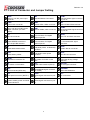
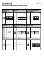
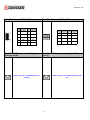
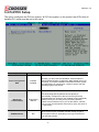
Revision: 2.0 AR-B5630 Board Socket P Intel® Core™2 Duo EPIC SBC with Intel® GME965 Express Chipset , DVI/LCD, Dual LAN and PCI-104 Eexpansion User Manual Manual Rev.: 2.0 Book Number: AR-B5630-2010.06.11 1 Revision: 2.0 Revision Version 2.0 Date Author 2010/06/11 Roger Nan Description Initial release 2 Revision: 2.0 Copyright 2010 All Rights Reserved. Manual’s first edition: June 11, 2010 For the purpose of improving reliability, design and function, the information in this document is subject to change without prior notice and does not represent a commitment on the part of the manufacturer. In no event will the manufacturer be liable for direct, indirect, special, incidental, or consequential damages arising out of the use or inability to use the product or documentation, even if advised of the possibility of such damages. This document contains proprietary information protected by copyright. All rights are reserved. No part of this Manual may be reproduced by any mechanical, electronic, or other means in any form without prior written permission of the manufacturer. Trademarks AR-B5630 is a registered trademarks of Acrosser; IBM PC is a registered trademark of the International Business Machines Corporation; Pentium is a registered trademark of Intel Technologies Inc; Award is a registered trademark of Award Software International Inc; other product names mentioned herein are used for identification purposes only and may be trademarks and/or registered trademarks of their respective companies. 3 Revision: 2.0 Table of Contents 1 Introduction .......................................................................................... 5 1.1 Features .......................................................................................................... 5 1.2 Package Contents .......................................................................................... 7 1.3 Block Diagram ................................................................................................ 8 2 H/W Information.................................................................................... 9 2.1 Locations......................................................................................................... 9 2.2 Connector and Jumper Setting Table ......................................................... 12 3 BIOS Setting ....................................................................................... 19 3.1 Main Setup .................................................................................................... 20 3.2 Advanced Chipset Setup ............................................................................. 21 3.3 Power Setup.................................................................................................. 22 3.4 PnP/PCI Setup............................................................................................... 23 3.5 Peripherals Setup ......................................................................................... 24 3.6 PC Health Setup............................................................................................ 25 3.7 Boot Setup .................................................................................................... 26 3.8 Exit Setup ...................................................................................................... 27 3.9 BIOS Update.................................................................................................. 29 Watch Dog Timer Reset Sample Code (IT8712F-A/IX-L)................ 30 NOTE 1: .............................................................................................. 32 4 Revision: 2.0 1 INTRODUCTION Welcome to the AR-B5630 ECIP AT/ATX Single Board Computer. The AR-B5630 is EPIC board with Socket P Intel Core™2 Duo or Core Duo or Core Solo and Celeron M processor and Intel GM965 + ICH8M Chipset. The memory contents one DDR2 SO-DIMM socket which supports up to 2GB of memory. Graphics display functionality is provided by Build-in Graphic Processor that supports CRT display and LVDS interface with Single or Dual channel panel specifications. Ethernet connectivity comes from the Intel WG82574L10/100/1000 M Ethernet controller. 1.1 Features Processor: Core 2 Duo, Core Duo and Celeron M Chipsets: GME965 + ICH8M Memory: DDR2 667MHz SO-DIMM, Maximum 2GB Display: VGA, DVI, LVDS, S-Video, BNC, Component video Storage: 1x CF, 1x SATA II, 1x IDE Audio: 5.1 CH Audio Realtek ALC662 Communication: 2x Gbps Ethernet, 4x USB 2.0, 3x RS-232, 1x RS-232/422/485 General: Watchdog timer, 8-bit GPIO, and PCI-104 expansion slot. Specifications Model Name Product Descriptions General CPU BIOS System Chipsets System Memory Watchdog Timer Battery Power Requirements Hardware monitoring ProtectU V 2.0 AR-B5630 EPIC SBC support 65nm Intel uFC-PGA 478 Core 2 Duo/Core Duo/Core Solo/Celeron M Processors with Dual Gigabit LANs / LCD / TV out / DVI Note Socket for Intel uFC-PGA 478 Core 2 Duo/Core Duo/Core Solo/Celeron M, Coolers required. AWARD Intel GM965 + ICH8M One SO-DIMM socket support 667/533 MHz DDR2 SDRAM up to 2GB Software programmable 1~255 Seconds Lithium Battery, 3V 220mAH For RTC Pin Header AT: 12V Single Voltage Input ATX: power switch pin header and pin header for external 5V stand-by input BIOS Support 1. CPU voltage 2. CPU and System Temperature 3. System and CPU FAN speed 4. System Fan Speed Control same as AR-B1892 (connector color different from CPU Fan connector) N/A 5 Revision: 2.0 LED Button Fan connector 2 LEDs for Power and HDD Power LED (Green), HDD (Orange) refer to AR-B1831 Reset button (use pin header) 1. CPU fan 2. System Fan with temperature controller (connector color different from CPU Fan connector) Win XP/XP Embedded, WinCE, Linux, Vista OS Video Graphic Controller Intel GM965 integrated GMA X3100 graphic controller VGA Memory: Intel DVMT 4.0 supports Max 224 MB shared video memory Dual Display CRT 1 x VGA port DVI 1 x DVI port TV Out 1 x TV Out (S-Video) LCD 1 x Dual Channel 18/24-bits LVDS Interface LCD inverter power connector and ON/OFF control Support 3.3V and 5V LCD Audio Audio Interface 5.1 CH Audio Realtek ALC662 Storage IDE 1 x E-IDE SSD 1 x Compact Flash Type-II FDC N/A SATA 1 x SATA interface One with standard SATA connector Network Interface Ethernet 1 x Intel WG82574L (10/100/1000Mbps) 1 x Intel WG82574L (10/100/1000Mbps) Boot on LAN, WOL I/O 1 x RS-232 (COM1) Serial Port 2 x RS-232 (COM3/4) 1 x RS-232/422/485 (COM2) Touch Screen N/A Parallel Port N/A GPIO 8 Independent TTL level I/O USB 2 x External ports 2 x Internal ports Audio Expansion slot Keyboard/ Mouse Mechanical Dimension Operating Temperature Storage Temperature Relative Humidity EMC & Safety EMC Safety 5.1 CH Audio 1 x PCI-104 (PCI Interface) 1 x PS/2 for Keyboard and Mouse PinHeader(2.0mm) D-Sub15 Pin Header Pin header Hirose Pin Header 44-Pin Header Type-II Socket 1xSATAConnector RJ45 DB9 Pin Header PinHeader (2x5x2.0) Connector Pin Header (1x5x2.0) Pin Header Slot Connector 115mm x 165mm (4.528 x 6.496 inches) 0~60oC (32~140oF) -20~80oC (-4~176oF) 0 to 90% @ 40°C, non-condensing (95% @ 40°C, Non-Condensing by request) CE, FCC Class A N/A 6 Revision: 2.0 1.2 Package Contents In addition to this User's Manual, the AR-B5630 package includes the following items: AR-B5630 AT/ATX Single Board Quick User Guide Utility CD(Include driver and Manual) Accessory set ACC-5630 series for purchase separately ATX POWER cable (PWR2/ CON2) x 1 DVI cable (DVI1) x 1 Audio cable (AUDIO1) x 1 USB Cable (with screws) x 1 PS/2 to PS/2 Y-cable (KM1) x 1 40/44-Pin IDE Cable X1 Serial port cable (COM) x 2 SATA HDD Cable (SATA1) x 1 SATA POWER cable (CON3) x 1 7 Revision: 2.0 1.3 Block Diagram 8 Revision: 2.0 2 H/W INFORMATION This chapter describes the installation of AR-B5631. At first, it shows the Function diagram and the layout of AR-B5630. It then describes the unpacking information which you should read carefully, as well as the jumper/switch settings for the AR-B5631 configuration. 2.1 Locations 2.1.1 Top Side 9 Revision: 2.0 2.1.2 Bottom Side 10 Revision: 2.0 2.1.3 List of Connector and Jumper Setting PWR2 External +12V DC power input connector. KM1 Keyboard/Mouse Connnector. COM1* External RS232 signal connector for port #1. CON2 ATX function connector. USB2 Internal USB2, USB3 connector. JP1 Select COM2 RS232/422/485. CON3 Extra +12V and +5V DC power output connector (for SATA device). USB1 External USB0, USB1 connector. COM2* RS-232/422/485 signal connector for port #2. J10 PCI-104 connector. LAN2 RJ45 connector for Gigabit Ethernet port #2. GPIO1 8-bit TTL-5V GPIO connector. JP2 Signal SERIRQ connects to PCI-104 pin #B2 selection. LAN1 RJ45 connector for Gigabit Ethernet port #1. AUDIO1 5.1 channels Audio signal connector. J5 CMOS data retention/clear. LCD1 LCD panel (LVDS, 18-bit/36-bit) connector. FAN2 System DC fan connector. BAT1 CMOS battery holder. LCDPW1 LCD panel inverter power connector. FAN1 CPU DC fan connector. SATA1 SATA device connector #1. VGA1 Pin Header for D-Sub 15 Pin VGA. J1 LCD panel driving voltage selection. J8 CF master or slave select. DVI1 Digital Video Interface (DVI-D). TVCON1 TV-out signal connector. IDE1 PATA connector(UATA-100). J9 RS422/RS485 signal connector (for COM2). SODIMM1 DDR2 SO-DIMM Slot. J12 Front panel connector. (NOTE 1) COM3* RS232 signal connector for port #3. CF1 CF card socket. D20 System standby power and HDD access indicators. COM4* RS232 signal connector for port #4. 11 Revision: 2.0 2.2 Connector and Jumper Setting Table 1. PWR2: External +12V DC power input connector. PIN 1 2 3 4 SETTING GND GND +12V +12V 4. J10: PCI-104 connector. 2. CON2: ATX function connector. PIN 1 2 3 5. JP2: Signal SERIRQ connects to PCI-104 pin #B2 selection. STATUS PCI-104 connector. 7. BAT1: CMOS battery holder. SETTING GND PS_ON +5V_SUS Open Short SETTING Disconnected. (Default) Connected. 8. SATA1: SATA device connector #2. 3. CON3: Extra +12V and +5V DC power output connector (for SATA device). PIN 1 2 3 4 6. J5: CMOS data retention/clear. STATUS Open Short SATA device connector #2. 12 SETTING Disconnected. (Default) Connected. 9. J8: CF master or slave select. STATUS CMOS battery holder. SETTING +12V GND +3.3V +5V SIGNAL SHORT MASTER OPEN SLAVE(Default) Revision: 2.0 10. IDE1: PATA connector. 11. J12: Front panel connector. (NOTE 1) PIN SIGNAL PIN SIGNAL 1 RESET 2 GND 3 D7 4 D8 5 D6 6 D9 7 D5 8 D10 9 D4 10 D11 11 D3 12 D12 13 D2 14 D13 15 D1 16 D14 17 D0 18 D15 19 GND 20 NC 21 DREQ 22 GND 23 IOW# 24 GND 25 IOR# 26 GND 27 IORDY 28 GND 29 DACK# 30 GND 31 IDEIRQ 32 NC 33 A1 34 PDIAG 35 A0 36 A2 37 DCS1# 38 CS3 39 IDE_LED# 40 GND 41 +5V 42 +5V 43 GND 44 NC 12. D20: System standby power and HDD access indicators. STATUS 1, 2 3, 4 5, 6 SETTING External buzzer. 1: Buzz + 2: Buzz Hardware reset Power button for ATX mode; jumper shorted for AT mode. 13. KM1: Keyboard/Mouse CONNECTOR Green: Standby power indicator. Yellow: HDD access indicator. Keyboard/Mouse connector. 13 Revision: 2.0 14. USB2: Internal USB2, USB3 connector. 15. USB1: External USB0, USB1 connector. PIN SIGNAL PIN SIGNAL 1 +5V 2 +5V 3 USB_3- 4 USB_2- 5 USB_3+ 6 USB_2+ 7 GND 8 GND 9 GND 10 GND 16. LAN2: RJ45 connector for Gigabit Ethernet port #2 PIN SIGNAL PIN SIGNAL 1 +5V 5 +5V 2 USB_1- 6 USB_0- 3 USB_1+ 7 USB_0+ 4 GND 8 GND 17. LAN1: RJ45 connector for Gigabit Ethernet port #1 RJ45 connector for Gigabit Ethernet port #2. RJ45 connector for Gigabit Ethernet port #1. 14 Revision: 2.0 18. LCD1: LCD panel (LVDS, 18-bit/36-bit) connector. PIN 1 3 5 7 9 11 13 15 17 19 21 23 25 27 29 SETTING LCD VDD E CLKGND E Data2+ E Data1NC E Data0+ GND O CLKO Data2+ I2C CLK O Data1O Data0+ NC LCD VDD PIN 2 4 6 8 10 12 14 16 18 20 22 24 26 28 30 19. LCDPW1: LCD panel inverter power connector. SETTING GND E CLK+ E Data2GND E Data1+ NC E Data0O CLK+ GND O Data2O Data1+ I2C Data O Data0NC LCD VDD PIN 1 2 3 4 5 6 SETTING +12V +12V GND BKL ON GND Reserved. E: Even for dual channel. O: Odd for single channel. 20. VGA1: Pin Header for D-Sub 15 Pin VGA. PIN SIGNAL PIN 21. DVI1: Digital Video Interface (DVI-D). PIN SIGNAL PIN SIGNAL 1 TD2- (Digital red-) 13 N.C 2 TD2+ (Digital red+) 14 +VCC 3 GND 15 GND 4 N.C 16 Hot plug detect 5 N.C17 TD0- (Digital blue-) 6 DDC clock 18 TD0+ (Digital blue+) 7 DDC data 19 GND 8 N.C 20 N.C 9 TD1- (Digital green-) 21 N.C 10 TD1+ (Digital green-) 22 GND 11 GND 23 TCLK- (Digital clock-) 12 N.C 24 TCLK+ (Digital clock+) SIGNAL 1 R 2 GND 3 G 4 GND 5 B 6 GND 7 VSYNC 8 SCL 9 HSYNC 10 SDA 15 Revision: 2.0 22. J9: RS422/RS485 signal connector (for COM2). PIN 1 2 3 4 23. COM3*: RS232 signal connector for port #3. SETTING RS485 DATA+ or RS422 TX+ RS485 DATAor RS422 TXRS422 RX+ RS422 RX- PIN SETTING PIN SETTING 1 DCD #2 2 DSR #2 3 RX #2 4 RTS #2 5 TX #2 6 CTS #2 7 DTR #2 8 RI #2 9 GND 10 NC 24. COM4*: RS232 signal connector for port 25. COM1*: RS-232 signal connector for port #4. #1. PIN SETTING PIN SETTING 1 DCD #3 2 DSR #3 3 RX #3 4 RTS #3 5 TX #3 6 CTS #3 7 DTR #3 8 RI #3 9 GND 10 NC 26. JP1: Select COM2 RS232/422/485. STATUS JP1 RS-232 1-2 RS-422 3-4 RS-485 5-6 D-SUB-9 male connector for RS232 port #1. 27. COM2*: RS232 signal connector for port #2. PIN SETTING PIN SETTING 1 DCD #2 2 DSR #2 3 RX #2 4 RTS #2 5 TX #2 6 CTS #2 7 DTR #2 8 RI #2 9 GND 10 NC 16 Revision: 2.0 28. GPIO1:8-bit TTL-5V GPIO connector. PIN 1 3 5 7 9 SETTING GPIO0 [30] GPIO1 [31] GPIO2 [32] GPIO3 [33] GND PIN 2 4 6 8 10 SETTING +5V GPIO7 [37] GPIO6 [36] GPIO5 [35] GPIO4 [34] 30. FAN2: System DC fan connector. PIN 1 2 3 29. AUDIO1: 5.1 channels Audio signal connector. PIN SETTING PIN SETTING 1 Line-out Right 2 Line-out Left 3 AGND 4 AGND 5 Line-in Right 6 Line-in Left 7 MIC-in 8 AGND 9 AGND 10 AGND 11 SR-out Right 12 SR-out Left 13 LFT-out 14 SEN-out 31. FAN1: CPU DC fan connector. SETTING GND +12V Fan speed data PIN 1 2 3 ON/OFF controlled by system temperature setting of BIOS. 17 SETTING GND +12V Sense Revision: 2.0 32. J1: LCD panel driving voltage selection. 33. TVCON1: STATUS 1-2 2-3 SETTING +5V for LCD panel. +3.3V for LCD panel. (Default). 34. SODIMM1: DDR2 SO-DIMM SLOT. TV-out signal connector. PIN SETTING PIN SETTING 1 Y-G 2 N/A 3 GND 4 N/A 5 CVBS/Pb-G 6 N/A 7 GND 8 N/A 9 C/Pr-G 10 N/A 11 GND 12 N/A 13 GND 14 N/A 35. CF1: CF CARD SOCKET. *:1. COM1 is the external UART RS-232 port, the text description on the PCB board is “CON1”. *:2. COM2 is the internal UART RS-232/422/485 port, the text description on the PCB board is “COM1”. *:3. COM3 is the internal UART RS-232 port, the text description on the PCB board is “COM2”. *:4. COM4 is the internal UART RS-232 port, the text description on the PCB board is “COM3”. 18 Revision: 2.0 3 BIOS SETTING This chapter describes the BIOS menu displays and explains how to perform common tasks needed to get the system up and running. It also gives detailed explanation of the elements found in each of the BIOS menus. The following topics are covered: Main Setup Advanced Chipset Setup Power Setup PnP/PCI Setup Peripherals Setup PC Health Setup Boot Setup Exit Setup Once you enter the Award BIOS™ CMOS Setup Utility, the Main Menu will appear on the screen. Use the arrow keys to highlight the item and then use the <Pg Up> <Pg Dn> keys to select the value you want in each item. 19 Revision: 2.0 3.1 Main Setup The <Main Setup> choice allows you to record some basic hardware configuration in your computer system and set the system clock and error handling. If the motherboard is already installed in a working system, you will not need to select this option. You will need to run this Setup option, however, if you change your system hardware configuration, the onboard battery fails, or the configuration stored in the COMS memory was lost or damaged. Note: Listed at the bottom of the menu are the control keys. If you need any help with the item fields, you can press the <F1> key, and it will display the relevant information. Option Choice Description Date Setup N/A Set the system date. Note that the ‘Day’ automatically changes when you set the date Time Setup N/A Set the system time IDE Channel 0 Master/Slave N/A The onboard IDE connectors provide 1 channel for connecting up to 2 IDE hard disks or other devices. The first is the “Master” and the second is “Slave”, BIOS will auto-detect the IDE type. Halt On All Errors, No Errors, All but keyboard. Select the situation in which you want the BIOS to stop the POST process and notify you. 20 Revision: 2.0 3.2 Advanced Chipset Setup This section allows you to configure and improve your system and follows you to set up some system features according to your preference. Option Choice Description Quick Power On Self Test Enabled Disabled This category speeds up Power On Self Test (POST) after you have powered up the computer. If it is set to Enable, BIOS will shorten or skip some check items during POST. Full Screen Logo Show Enabled Disabled Select Enabled to show the OEM full screen logo if you have add-in BIOS. VGA Share Memory Size 1M 8M Boot Display CRT DVI LCD TV CRT+DVI CRT+LCD CRT+TV This Item is for setting the Frame Buffer (Share system memory as display memory). This Item is to set display device 21 Revision: 2.0 3.3 Power Setup Use this main to specify your setting for power management. Option Choice ACPI Function Enabled Disabled Enable this function to support ACPI (Advance Configuration and Power Interface). S1 (POS) S3 (STR) S1+S3. This options for this field are S1 (POS) and S3 (STR). By default, the field is set to S1 (POS) PWRON After PWR-Fail. ACPI Suspend Type Power –Supply Type AT ATX Description This item allows you to choose the Type of Power Supply in use.The Choice: AT, ATX. 22 Revision: 2.0 3.4 PnP/PCI Setup The option configures the PCI bus system. All PCI bus system on the system use INT#, thus all installed PCI cards must be set to this value. Option Choice Description Enabled Disabled Normally, you leave this field Disabled. Select Enabled to reset Extended System Configuration Data (ESCD) when you exit Setup. If you have installed a new add-on and the system reconfiguration has caused such a serious conflict, then the operating system cannot boot. Resources Controlled By Auto(ESCD) Manual The Award Plug and Play BIOS has the capacity to automatically configure all of the boot and Plug and Play compatible devices. However, this capability means absolutely nothing unless you are using a Plug and Play operating system such as Windows 95. If you set this field to “manual,” then you may choose specific resources by going into each of the submenus. IRQ Resources N/A Reset Configuration Data When resources are controlled manually, assign a type to each system interrupt, depending on the type of the device that uses the interrupt 23 Revision: 2.0 3.5 Peripherals Setup This option controls the configuration of the board’s chipset. Control keys for this screen are the same as for the previous screen. Option Onboard Serial Port 1 Onboard Serial Port 2 Onboard Serial Port 3 Onboard Serial Port 4 Choice Serial Port 1: 3F8 / IRQ11 Serial Port 2: 2F8 / IRQ10 Serial Port 3: 3E8 / IRQ9 Serial Port 4: 2e8 / IRQ8 USB Device Setting Enabled Disabled Description Select an address and the corresponding interrupt for each serial port. Select Enabled if your system contains a Universal Serial Bus (USB) 2.0 controller and you have USB peripherals The integrated peripheral controller contains an IDE interface with support for two IDE channels. Select Enabled to activate each channel separately. On chip IDE DEVICE 24 Revision: 2.0 3.6 PC Health Setup This section shows the parameters in determining the PC Health Status. These parameters include temperatures, fan speeds, and voltages. 25 Revision: 2.0 3.7 Boot Setup This section is used to exit the BIOS main menu. After making your changes, you can either save them or exit the BIOS menu and without saving the new values. Option First / Second / Third Boot Device/Other Boot Device Hard Disk Boot Priority Choice Hard Disk CDROM USB-FDD USB-CDROM Disabled Description The BIOS attempts to load the operating system from the devices in the sequence selected in these items. These fields set the Boot Priority for each Hard Disk (SATA/IDE HDD and USB Flash) N/A 26 Revision: 2.0 3.8 Exit Setup This section is used to configure exit mode. Option Choice Description Pressing <Enter> on this item for confirmation: Save & Exit Setup Save to CMOS and EXIT (Y/N)? Y Load Optimized Defaults When you press <Enter> on this item you get a confirmation dialog box with a message like this: Press “Y” to store the selections made in the menus in CMOS – a special section of memory that stays on after you turn your system off. The next time you boot your computer, the BIOS configures your system according to the Setup selections stored in CMOS. After saving the values the system is restarted again Press ‘Y’ to load the default values that are factory-set for optimal-performance system operations. Load Optimized Defaults (Y/N)? N Exit Without Saving Pressing <Enter> on this item for confirmation: Quit without saving (Y/N)? Y 27 This allows you to exit Setup without storing any changes in CMOS. The previous selections remain in effect. This shall exit the Setup utility and restart your computer. Revision: 2.0 When a password has been enabled, you will be prompted to enter your password every time you try to enter Setup. This prevents unauthorized persons from changing any part of your system configuration. Set Password Pressing <Enter> on this item for confirmation: ENTER PASSWORD: Type the password, up to eight characters in length, and press <Enter>. The password typed now will clear any previous password from the CMOS memory. You will be asked to confirm the password. Type the password again and press <Enter>. You may also press <Esc> to abort the selection and not enter a password. To disable a password, just press <Enter> when you are prompted to enter the password. A message will confirm that the password will be disabled. Once the password is disabled, the system will boot and you can enter Setup freely. 28 Revision: 2.0 3.9 BIOS Update The BIOS program instructions are contained within computer chips called FLASH ROMs that are located on your system board. The chips can be electronically reprogrammed, allowing you to upgrade your BIOS firmware without removing and installing chips. The AR-B5630 provides the FLASH BIOS update function for you to easily to update to a newer BIOS version. Please follow these operating steps to update to new BIOS: Step 1: Turn on your system and don’t detect the CONFIG.SYS and AUTOEXEC.BAT files. Step 2: You will get AWDFLASH.EXE and XXXXXX.BIN , please copy them to the boot disk . Step 3: In the MS-DOS mode, you can type the AWDFLASH and press [ ENTER ] . A:\> AWDFLASH Step 4: A window will appear and ask you to type the complete BIOS file ( xxxxxx.BIN ) and press [ ENTER ] . Step 5: Then it will ask whether you save the old BIOS file , you can choose the YES or NO . Step 6: Then it will ask you whether want to program it , please choose YES . Step 7: The BIOS will start to upgrade Step 8: When you have successfully flashed the BIOS then press the[F1] to reboot the Computer and hit [DEL] to enter the BIOS CMOS SETTING . Select " LOAD S-STUP DEFAULTS " set as YES . Then save and exit the setting Note: 1. In order to prevent your system from hanging up during flashing BIOS , please check the new BIOS match your model name and current BIOS version . 2. In order to protect your motherboard , please don’t turn off your computer during the flashing or it will damage your BIOS ROM . 29 Revision: 2.0 Watch Dog Timer Reset Sample Code (IT8712F-A/IX-L) The WDT (Watch Dog Timer) is used to generate a variety of output signals after a user programmable count. The WDT is suitable for use in the prevention of system lock-up, such as when software becomes trapped in a deadlock. Under these sorts of circumstances, the timer will count to zero and the selected outputs will be driven. Under normal circumstance, the user will restart the WDT at regular intervals before the timer counts to zero. The watchdog timer is a circuit that maybe used from your program software to detect crash or hang up. The Watchdog timer is automatically disabled after reset. Once you enabled the watchdog timer, your program should trigger the watchdog timer every time before it times out. After you trigger the watchdog timer, the timer will be set to zero and start to count again. If your program fails to trigger the watchdog timer before times out, it will generate a reset pulse to reset the system or trigger the IRQ 9 signal in order to tell your system that the watchdog time is out. User could test watchdog function under ‘Debug’ program as follows: C:>debug o 2E 87 ;Extended Functions Enable Register o 2E 01 ;Extended Functions Enable Register o 2E 55 ; Extended Functions Enable Register o 2E 55 ; Extended Functions Enable Register o 2E 07 ;EFIR=EFER (Extended Functions Index Register) point to Logical Device Number Reg. o 2F 07 ; Select logical device 7, (Watchdog Function) o 2E 23 ; Clock Source Select of Watch Dog Timer o 2F 10 ; Select Eeternal CLKIN o 2E 72 ; Select Watchdog count mode seconds or minutes o 2F C0 ; Default is second and KBRST mode. o 2E 73 ; Select Watchdog Timer Value o 2F 08 ;update CRF6 with value 08H ,(8sec reset) 30 Revision: 2.0 // Set Watchdog outportb(IO_Port_Address,0x07); // Point to Logical Device Number Reg. outportb(IO_Port_Address+1,0x07); // Select logical device 7, (Watchdog Function) outportb(IO_Port_Address,0x23); // Select Watchdog use CLKIN outportb(IO_Port_Address+1,inportb(IO_Port_Address+1)|0x10); outportb(IO_Port_Address,0x72); // Select Watchdog use keyboard reset outportb(IO_Port_Address+1,0x40); outportb(IO_Port_Address,0x72); // Select Watchdog count mode seconds or minutes outportb(IO_Port_Address+1,inportb(IO_Port_Address+1)|0x80); // Set Second outportb(IO_Port_Address,0x73); // Set Watchdog Timer Value outportb(IO_Port_Address+1,Time); // 0x00 to disable, max 0xFF 31 Revision: 2.0 NOTE 1: J12: Front panel connector. STATUS 1, 2 3, 4 5, 6 SETTING External buzzer. 5: Buzz + 6: Buzz Hardware reset Power button for ATX mode; jumper shorted for AT mode. When using AT mode in the system, the pin9-10 of header J12 must be shorted. If using ATX mode in the system, the pin5-6 of header J12 should connect to a Push-Button-Switch. NOTE: When using AT mode, the monitor will not display any message and the system will not auto-shut down after soft-off. In this case, please cut the PSU’s power off or remove PSU’s power to cut the system power off. 32