1
Introduction to the Altera
Nios II Soft Processor
For Quartus II 13.0
1
Introduction
This tutorial presents an introduction to Altera’s Nios® II processor, which is a soft processor that can be instantiated
on an Altera FPGA device. It describes the basic architecture of Nios II and its instruction set. The Nios II processor
and its associated memory and peripheral components are easily instantiated by using Altera’s SOPC Builder or
Qsys tool in conjuction with the Quartus® II software.
A full desciption of the Nios II processor is provided in the Nios II Processor Reference Handbook, which is available
in the literature section of the Altera web site. Introductions to the SOPC Builder and Qsys tools are given in the
tutorials Introduction to the Altera SOPC Builder and Introduction to the Altera Qsys System Integration Tool,
respectively. Both can be found in the University Program section of the web site.
Contents:
• Nios II System
• Overview of Nios II Processor Features
• Register Structure
• Accessing Memory and I/O Devices
• Addressing
• Instruction Set
• Assembler Directives
• Example Program
• Exception Processing
• Cache Memory
• Tightly Coupled Memory
Altera Corporation - University Program
May 2013
1
I NTRODUCTION TO THE A LTERA N IOS II S OFT P ROCESSOR
2
For Quartus II 13.0
Background
Altera’s Nios II is a soft processor, defined in a hardware description language, which can be implemented in
Altera’s FPGA devices by using the Quartus® II CAD system. This tutorial provides a basic introduction to the Nios
II processor, intended for a user who wishes to implement a Nios II based system on an Altera Development and
Education board.
3
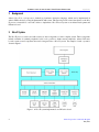
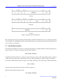
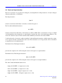
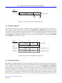
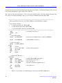
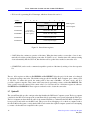
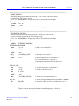
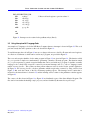
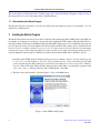
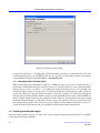
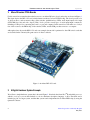
Nios II System
The Nios II processor can be used with a variety of other components to form a complete system. These components
include a number of standard peripherals, but it is also possible to define custom peripherals. Altera’s DE-series
boards contain several components that can be integrated into a Nios II system. An example of such a system is
shown in Figure 1.
Figure 1. A Nios II system implemented on a DE-series board.
2
Altera Corporation - University Program
May 2013
I NTRODUCTION TO THE A LTERA N IOS II S OFT P ROCESSOR
For Quartus II 13.0
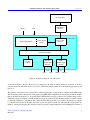
The Nios II processor and the interfaces needed to connect to other chips on the board are implemented in the FPGA
chip. These components are interconnected by means of the interconnection network called the Avalon Switch
Fabric. Memory blocks in the FPGA device can be used to provide an on-chip memory for the Nios II processor.
They can be connected to the processor either directly or through the Avalon network. The SRAM and SDRAM
memory chips on the board are accessed through the appropriate interfaces. Input/output interfaces are instantiated
to provide connection to the I/O devices used in the system. A special JTAG UART interface is used to connect to
the circuitry that provides a Universal Serial Bus (USB) link to the host computer to which the DE-series board is
connected. This circuitry and the associated software is called the USB-Blaster. Another module, called the JTAG
Debug module, is provided to allow the host computer to control the Nios II processor. It makes it possible to
perform operations such as downloading programs into memory, starting and stopping execution, setting program
breakpoints, and collecting real-time execution trace data.
Since all parts of the Nios II system implemented on the FPGA chip are defined by using a hardware description
language, a knowledgeable user could write such code to implement any part of the system. This would be an
onnerous and time consuming task. Instead, one can use the SOPC Builder or Qsys tools in the Quartus II software
to implement a desired system simply by choosing the required components and specifying the parameters needed
to make each component fit the overall requirements of the system.
4
Overview of Nios II Processor Features
The Nios II processor has a number of features that can be configured by the user to meet the demands of a desired
system. The processor can be implemented in three different configurations:
• Nios II/f is a "fast" version designed for superior performance. It has the widest scope of configuration options
that can be used to optimize the processor for performance.
• Nios II/s is a "standard" version that requires less resources in an FPGA device as a trade-off for reduced
performance.
• Nios II/e is an "economy" version which requires the least amount of FPGA resources, but also has the most
limited set of user-configurable features.
The Nios II processor has a Reduced Instruction Set Computer (RISC) architecture. Its arithmetic and logic operations are performed on operands in the general purpose registers. The data is moved between the memory and these
registers by means of Load and Store instructions.
The wordlength of the Nios II processor is 32 bits. All registers are 32 bits long. Byte addresses in a 32-bit word are
assigned in little-endian style, in which the lower byte addresses are used for the less significant bytes (the rightmost
bytes) of the word. The Nios II architecture uses separate instruction and data buses, which is often referred to as
the Harvard architecture.
A Nios II processor may operate in the following modes:
• Supervisor mode – allows the processor to execute all instructions and perform all available functions. When
the processor is reset, it enters this mode.
Altera Corporation - University Program
May 2013
3
I NTRODUCTION TO THE A LTERA N IOS II S OFT P ROCESSOR
For Quartus II 13.0
• User mode – the intent of this mode is to prevent execution of some instructions that shoud be used for systems
purposes only. This mode is available only when the processor is configured to use the Memory Management
Unit (MMU) or the Memory Protection Unit (MPU).
Application programs can be run in either the User or Supervisor modes.
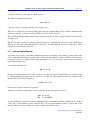
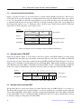
5
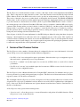
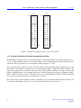
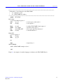
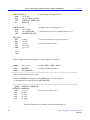
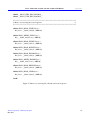
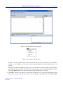
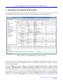
Register Structure
The Nios II processor has thirty-two 32-bit general-purpose registers, as shown in Figure 2. Some of these registers
are intended for a specific purpose and have special names that are recognized by the Assembler.
• Register r0 is referred to as the zero register. It always contains the constant 0. Thus, reading this register
returns the value 0, while writing to it has no effect.
• Register r1 is used by the Assembler as a temporary register; it should not be referenced in user programs
• Registers r24 and r29 are used for processing of exceptions; they are not available in User mode
• Registers r25 and r30 are used exclusively by the JTAG Debug module
• Registers r27 and r28 are used to control the stack used by the Nios II processor
• Register r31 is used to hold the return address when a subroutine is called
Register
r0
r1
r2
r3
Name
zero
at
Function
0x00000000
Assembler Temporary
·
·
·
·
·
·
·
·
·
r23
r24
et
Exception Temporary (1)
r25
bt
Breakpoint Temporary (2)
r26
gp
Global Pointer
r27
sp
Stack Pointer
r28
fp
Frame Pointer
r29
ea
Exception Return Address (1)
r30
ba
Breakpoint Return Address (2)
r31
ra
Return Address
(1) The register is not available in User mode
(2) The register is used exclusively by the JTAG Debug module
Figure 2. General-purpose registers.
4
Altera Corporation - University Program
May 2013
I NTRODUCTION TO THE A LTERA N IOS II S OFT P ROCESSOR
For Quartus II 13.0
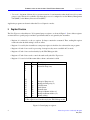
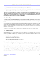
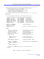
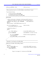
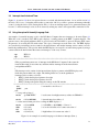
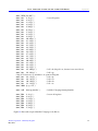
Nios II can have a number of 32-bit control registers. The number of registers depends on whether the MMU or the
MPU features are implemented. There are six basic control registers, as indicated in Figure 3. The names given in
the figure are recognized by the Assembler. The registers are used as follows:
• Register ctl0 reflects the operating status of the processor. Two bits of this register are always used:
– U is the User/Supervisor mode bit; U = 1 for User mode, while U = 0 for Supervisor mode.
– PIE is the processor interrupt-enable bit. When PIE = 1, the processor may accept external interrupts.
When PIE = 0, the processor ignores external interrupts.
The rest of the bits (labeled as reserved in the figure) are used when MMU or MPU features are implemented.
• Register ctl1 holds a saved copy of the status register during exception processing. The bits EU and EPIE are
the saved values of the status bits U and PIE.
• Register ctl2 holds a saved copy of the status register during debug break processing. The bits BU and BPIE
are the saved values of the status bits U and PIE.
• Register ctl3 is used to enable individual external interrupts. Each bit corresponds to one of the interrupts irq0
to irq31. The value of 1 means that the interrupt is enabled, while 0 means that it is disabled.
• Register ctl4 indicates which interrupts are pending. The value of a given bit, c t l 4k , is set to 1 if the interrupt
irqk is both active and enabled by having the interrupt-enable bit, c t l 3k , set to 1.
• Register ctl5 holds a value that uniquely identifies the processor in a multiprocessor system.
Register
ctl0
ctl1
ctl2
ctl3
ctl4
ctl5
Name
status
estatus
bstatus
ienable
ipending
cpuid
b 31
···
b2
b1
b0
Reserved
U
PIE
Reserved
EU EPIE
Reserved
BU BPIE
Interrupt-enable bits
Pending-interrupt bits
Unique processor identifier
Figure 3. Basic control registers.
The control registers can be read from and written to by special instructions rdctl and wrctl, which can be executed
only in the supervisor mode.
6
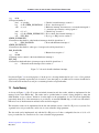
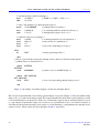
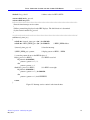
Accessing Memory and I/O Devices
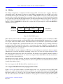
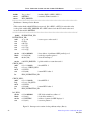
Figure 4 shows how a Nios II processor can access memory and I/O devices. For best performance, the Nios II/f
processor can include both instruction and data caches. The caches are implemented in the FPGA memory blocks.
Their usage is optional and they are specified (including their size) at the system generation time by using the SOPC
Altera Corporation - University Program
May 2013
5
I NTRODUCTION TO THE A LTERA N IOS II S OFT P ROCESSOR
For Quartus II 13.0
Builder or Qsys. The Nios II/s version can have the instruction cache but not the data cache. The Nios II/e version
has neither the instruction nor data cache.
Another way to give the processor fast access to the on-chip memory is by using the tightly coupled memory arrangement, in which case the processor accesses the memory via a direct path rather than through the Avalon network.
Accesses to a tightly coupled memory bypass the cache memory. There can be one or more tightly coupled instruction and data memories. If the instruction cache is not included in a system, then there must be at least one tightly
coupled memory provided for Nios II/f and Nios II/s processors. On-chip memory can also be accessed via the
Avalon network.
Off-chip memory devices, such as SRAM, SDRAM, and Flash memory chips are accessed by instantiating the
appropriate interfaces. The input/output devices are memory mapped and can be accessed as memory locations.
Data accesses to memory locations and I/O interfaces are performed by means of Load and Store instructions, which
cause data to be transferred between the memory and general-purpose registers.
Figure 4. Memory and I/O organization.
6
Altera Corporation - University Program
May 2013
I NTRODUCTION TO THE A LTERA N IOS II S OFT P ROCESSOR
7
For Quartus II 13.0
Addressing
The Nios II processor issues 32-bit addresses. The memory space is byte-addressable. Instructions can read and
write words (32 bits), halfwords (16 bits), or bytes (8 bits) of data. Reading or writing to an address that does not
correspond to an existing memory or I/O location produces an undefined result.
There are five addressing modes provided:
• Immediate mode – a 16-bit operand is given explicitly in the instruction. This value may be sign extended to
produce a 32-bit operand in instructions that perform arithmetic operations.
• Register mode – the operand is in a processor register
• Displacement mode – the effective address of the operand is the sum of the contents of a register and a signed
16-bit displacement value given in the instruction
• Register indirect mode – the effective address of the operand is the contents of a register specified in the
instruction. This is equivalent to the displacement mode where the displacement value is equal to 0.
• Absolute mode – a 16-bit absolute address of an operand can be specified by using the displacement mode
with register r0 which always contains the value 0.
8
Instructions
All Nios II instructions are 32-bits long. In addition to machine instructions that are executed directly by the processor, the Nios II instruction set includes a number of pseudoinstructions that can be used in assembly language
programs. The Assembler replaces each pseudoinstruction by one or more machine instructions.
Figure 5 depicts the three possible instruction formats: I-type, R-type and J-type. In all cases the six bits b5−0 denote
the OP code. The remaining bits are used to specify registers, immediate operands, or extended OP codes.
• I-type – Five-bit fields A and B are used to specify general-purpose registers. A 16-bit field IMMED16
provides immediate data which can be sign extended to provide a 32-bit operand.
• R-type – Five-bit fields A, B and C are used to specify general-purpose registers. An 11-bit field OPX is used
to extend the OP code.
• J-type – A 26-bit field IMMED26 contains an unsigned immediate value. This format is used only in the Call
instruction.
Altera Corporation - University Program
May 2013
7
I NTRODUCTION TO THE A LTERA N IOS II S OFT P ROCESSOR
For Quartus II 13.0
Figure 5. Formats of Nios II instructions.
The following subsections discuss briefly the main features of the Nios II instruction set. For a complete description
of the instruction set, including the details of how each instruction is encoded, the reader should consult the Nios II
Processor Reference Handbook.
8.1
Load and Store Instructions
Load and Store instructions are used to move data between memory (and I/0 interfaces) and the general-purpose
registers. They are of I-type. For example, the Load Word instruction
ldw rB, byte_offset(rA)
determines the effective address of a memory location as the sum of a byte_offset value and the contents of register
A . The 16-bit byte_offset value is sign extended to 32 bits. The 32-bit memory operand is loaded into register B .
For instance, assume that the contents of register r 4 are 126010 and the byte_offset value is 8010 . Then, the instruction
ldw r3, 80(r4)
loads the 32-bit operand at memory address 134010 into register r 3.
The Store Word instruction has the format
stw rB, byte_offset(rA)
8
Altera Corporation - University Program
May 2013
I NTRODUCTION TO THE A LTERA N IOS II S OFT P ROCESSOR
For Quartus II 13.0
It stores the contents of register B into the memory location at the address computed as the sum of the byte_offset
value and the contents of register A .
There are Load and Store instructions that use operands that are only 8 or 16 bits long. They are referred to as
Load/Store Byte and Load/Store Halfword instructions, respectively. Such Load instructions are:
• ldb (Load Byte)
• ldbu (Load Byte Unsigned)
• ldh (Load Halfword)
• ldhu (Load Halfword Unsigned)
When a shorter operand is loaded into a 32-bit register, its value has to be adjusted to fit into the register. This is done
by sign extending the 8- or 16-bit value to 32 bits in the ldb and ldh instructions. In the ldbu and ldhu instructions
the operand is zero extended.
The corresponding Store instructions are:
• stb (Store Byte)
• sth (Store Halfword)
The stb instruction stores the low byte of register B into the memory byte specified by the effective address. The
sth instruction stores the low halfword of register B . In this case the effective address must be halfword aligned.
Each Load and Store instruction has a version intended for accessing locations in I/O device interfaces. These
instructions are:
• ldwio (Load Word I/O)
• ldbio (Load Byte I/O)
• ldbuio (Load Byte Unsigned I/O)
• ldhio (Load Halfword I/O)
• ldhuio (Load Halfword Unsigned I/O)
• stwio (Store Word I/O)
• stbio (Store Byte I/O)
• sthio (Store Halfword I/O)
The difference is that these instructions bypass the cache, if one exists.
Altera Corporation - University Program
May 2013
9
I NTRODUCTION TO THE A LTERA N IOS II S OFT P ROCESSOR
8.2
For Quartus II 13.0
Arithmetic Instructions
The arithmetic instructions operate on the data that is either in the general purpose registers or given as an immediate
value in the instruction. These instructions are of R-type or I-type, respectively. They include:
• add (Add Registers)
• addi (Add Immediate)
• sub (Subtract Registers)
• subi (Subtract Immediate)
• mul (Multiply)
• muli (Multiply Immediate)
• div (Divide)
• divu (Divide Unsigned)
The Add instruction
add rC, rA, rB
adds the contents of registers A and B , and places the sum into register C .
The Add Immediate instruction
addi rB, rA, IMMED16
adds the contents of register A and the sign-extended 16-bit operand given in the instruction, and places the result
into register B . The addition operation in these instructions is the same for both signed and unsigned operands;
there are no condition flags that are set by the operation. This means that when unsigned operands are added, the
carry from the most significant bit position has to be detected by executing a separate instruction. Similarly, when
signed operands are added, the arithmetic overflow has to be detected separately. The detection of these conditions
is dicussed in section 8.11.
The Subtract instruction
sub rC, rA, rB
subtracts the contents of register B from register A , and places the result into register C . Again, the carry and
overflow detection has to be done by using additional instructions, as explained in section 8.11.
The immediate version, subi, is a pseudoinstruction implemented as
10
Altera Corporation - University Program
May 2013
I NTRODUCTION TO THE A LTERA N IOS II S OFT P ROCESSOR
For Quartus II 13.0
addi rB, rA, -IMMED16
The Multiply instruction
mul rC, rA, rB
multiplies the contents of registers A and B , and places the low-order 32 bits of the product into register C . The
operands are treated as unsigned numbers. The carry and overflow detection has to be done by using additional
instructions. In the immediate version
muli rB, rA, IMMED16
the 16-bit immediate operand is sign extended to 32 bits.
The Divide instruction
div rC, rA, rB
divides the contents of register A by the contents of register B and places the integer portion of the quotient into
register C . The operands are treated as signed integers. The divu instruction is performed in the same way except
that the operands are treated as unsigned integers.
8.3
Logic Instructions
The logic instructions provide the AND, OR, XOR, and NOR operations. They operate on data that is either in
the general purpose registers or given as an immediate value in the instruction. These instructions are of R-type or
I-type, respectively.
The AND instruction
and rC, rA, rB
performs a bitwise logical AND of the contents of registers A and B , and stores the result in register C . Similarly,
the instructions or, xor and nor perform the OR, XOR and NOR operations, respectively.
The AND Immediate instruction
andi rB, rA, IMMED16
performs a bitwise logical AND of the contents of register A and the IMMED16 operand which is zero-extended to
32 bits, and stores the result in register B . Similarly, the instructions ori, xori and nori perform the OR, XOR and
NOR operations, respectively.
Altera Corporation - University Program
May 2013
11
I NTRODUCTION TO THE A LTERA N IOS II S OFT P ROCESSOR
For Quartus II 13.0
It is also possible to use the 16-bit immediate operand as the 16 high-order bits in the logic operations, in which case
the low-order 16 bits of the operand are zeros. This is accomplished with the instructions:
• andhi (AND High Immediate)
• orhi (OR High Immediate)
• xorhi (XOR High Immediate)
8.4
Move Instructions
The Move instructions copy the contents of one register into another, or they place an immediate value into a register.
They are pseudoinstructions implemented by using other instructions. The instruction
mov rC, rA
copies the contents of register A into register C . It is implemented as
add rC, rA, r0
The Move Immediate instruction
movi rB, IMMED16
sign extends the IMMED16 value to 32 bits and loads it into register B . It is implemented as
addi rB, r0, IMMED16
The Move Unsigned Immediate instruction
movui rB, IMMED16
zero extends the IMMED16 value to 32 bits and loads it into register B . It is implemented as
ori rB, r0, IMMED16
The Move Immediate Address instruction
movia rB, LABEL
12
Altera Corporation - University Program
May 2013
I NTRODUCTION TO THE A LTERA N IOS II S OFT P ROCESSOR
For Quartus II 13.0
loads a 32-bit value that corresponds to the address LABEL into register B . It is implemented as:
orhi
ori
rB, r0, %hi(LABEL)
rB, rB, %lo(LABEL)
The %hi(LABEL) and %lo(LABEL) are the Assembler macros which extract the high-order 16 bits and the loworder 16 bits, respectively, of a 32-bit value LABEL. The orhi instruction sets the high-order bits of register B ,
followed by the ori instruction which sets the low-order bits of B . Note that two instructions are used because the
I-type format provides for only a 16-bit immediate operand.
8.5
Comparison Instructions
The Comparison instructions compare the contents of two registers or the contents of a register and an immediate
value, and write either 1 (if true) or 0 (if false) into the result register. They are of R-type or I-type, respectively.
These instructions correspond to the equality and relational operators in the C programming language.
The Compare Less Than Signed instruction
cmplt rC, rA, rB
performs the comparison of signed numbers in registers A and B , rA < rB, and writes a 1 into register C if the result
is true; otherwise, it writes a 0.
The Compare Less Than Unsigned instruction
cmpltu rC, rA, rB
performs the same function as the cmplt instruction, but it treats the operands as unsigned numbers.
Other instructions of this type are:
• cmpeq rC, rA, rB (Comparison rA == rB)
• cmpne rC, rA, rB (Comparison rA != rB)
• cmpge rC, rA, rB (Signed comparison rA >= rB)
• cmpgeu rC, rA, rB (Unsigned comparison rA >= rB)
• cmpgt rC, rA, rB (Signed comparison rA > rB)
This is a pseudoinstruction implemented as the cmplt instruction by swapping its rA and rB operands.
• cmpgtu rC, rA, rB (Unsigned comparison rA > rB)
This is a pseudoinstruction implemented as the cmpltu instruction by swapping its rA and rB operands.
Altera Corporation - University Program
May 2013
13
I NTRODUCTION TO THE A LTERA N IOS II S OFT P ROCESSOR
For Quartus II 13.0
• cmple rC, rA, rB (Signed comparison rA <= rB)
This is a pseudoinstruction implemented as the cmpge instruction by swapping its rA and rB operands.
• cmpleu rC, rA, rB (Unsigned comparison rA <= rB)
This is a pseudoinstruction implemented as the cmpgeu instruction by swapping its rA and rB operands.
The immediate versions of the Comparison instructions involve an immediate operand. For example, the Compare
Less Than Signed Immediate instruction
cmplti rB, rA, IMMED16
compares the signed number in register A with the sign-extended immediate operand. It writes a 1 into register B if
rA < IMMED16; otherwise, it writes a 0.
The Compare Less Than Unsigned Immediate instruction
cmpltui rB, rA, IMMED16
compares the unsigned number in register A with the zero-extended immediate operand. It writes a 1 into register B
if rA < IMMED16; otherwise, it writes a 0.
Other instructions of this type are:
• cmpeqi rB, rA, IMMED16 (Comparison rA == IMMED16)
• cmpnei rB, rA, IMMED16 (Comparison rA != IMMED16)
• cmpgei rB, rA, IMMED16 (Signed comparison rA >= IMMED16)
• cmpgeui rB, rA, IMMED16 (Unsigned comparison rA >= IMMED16)
• cmpgti rB, rA, IMMED16 (Signed comparison rA > IMMED16)
This is a pseudoinstruction which is implemented by using the cmpgei instruction with an immediate value
IMMED16 + 1.
• cmpgtui rB, rA, IMMED16 (Unsigned comparison rA > IMMED16)
This is a pseudoinstruction which is implemented by using the cmpgeui instruction with an immediate value
IMMED16 + 1.
• cmplei rB, rA, IMMED16 (Signed comparison rA <= IMMED16)
This is a pseudoinstruction which is implemented by using the cmplti instruction with an immediate value
IMMED16 + 1.
• cmpleui rB, rA, IMMED16 (Unsigned comparison rA <= IMMED16)
This is a pseudoinstruction which is implemented by using the cmpltui instruction with an immediate value
IMMED16 + 1.
14
Altera Corporation - University Program
May 2013
I NTRODUCTION TO THE A LTERA N IOS II S OFT P ROCESSOR
8.6
For Quartus II 13.0
Shift Instructions
The Shift instructions shift the contents of a register either to the right or to the left. They are of R-type. They
correspond to the shift operators, >> and <<, in the C programming language. These instructions are:
• srl rC, rA, rB (Shift Right Logical)
• srli rC, rA, IMMED5 (Shift Right Logical Immediate)
• sra rC, rA, rB (Shift Right Arithmetic)
• srai rC, rA, IMMED5 (Shift Right Arithmetic Immediate)
• sll rC, rA, rB (Shift Left Logical)
• slli rC, rA, IMMED5 (Shift Left Logical Immediate)
The srl instruction shifts the contents of register A to the right by the number of bit positions specified by the five
least-significant bits (number in the range 0 to 31) in register B , and stores the result in register C . The vacated bits
on the left side of the shifted operand are filled with 0s.
The srli instruction shifts the contents of register A to the right by the number of bit positions specified by the five-bit
unsigned value, IMMED5, given in the instruction.
The sra and srai instructions perform the same actions as the srl and srli instructions, except that the sign bit, r A 31 ,
is replicated into the vacated bits on the left side of the shifted operand.
The sll and slli instructions are similar to the srl and srli instructions, but they shift the operand in register A to the
left and fill the vacated bits on the right side with 0s.
8.7
Rotate Instructions
There are three Rotate instructions, which use the R-type format:
• ror rC, rA, rB (Rotate Right)
• rol rC, rA, rB (Rotate Left)
• roli rC, rA, IMMED5 (Rotate Left Immediate)
The ror instruction rotates the bits of register A in the left-to-right direction by the number of bit positions specified
by the five least-significant bits (number in the range 0 to 31) in register B , and stores the result in register C .
The rol instruction is similar to the ror instruction, but it rotates the operand in the right-to-left direction.
The roli instruction rotates the bits of register A in the right-to-left direction by the number of bit positions specified
by the five-bit unsigned value, IMMED5, given in the instruction, and stores the result in register C .
Altera Corporation - University Program
May 2013
15
I NTRODUCTION TO THE A LTERA N IOS II S OFT P ROCESSOR
8.8
For Quartus II 13.0
Branch and Jump Instructions
The flow of execution of a program can be changed by executing Branch or Jump instructions. It may be changed
either unconditionally or conditionally.
The Jump instruction
jmp rA
transfers execution unconditionally to the address contained in register A .
The Unconditional Branch instruction
br LABEL
transfers execution unconditionally to the instruction at address LABEL. This is an instruction of I-type, in which
a 16-bit immediate value (interpreted as a signed number) specifies the offset to the branch target instruction. The
offset is the distance in bytes from the instruction that immediately follows br to the address LABEL.
Conditional transfer of execution is achieved with the Conditional Branch instructions, which compare the contents
of two registers and cause a branch if the result is true. These instructions are of I-type and the offset is determined
as explained above for the br instruction.
The Branch if Less Than Signed instruction
blt rA, rB, LABEL
performs the comparison rA < rB, treating the contents of the registers as signed numbers.
The Branch if Less Than Unsigned instruction
bltu rA, rB, LABEL
performs the comparison rA < rB, treating the contents of the registers as unsigned numbers.
The other Conditional Branch instructions are:
• beq rA, rB, LABEL (Comparison rA == rB)
• bne rA, rB, LABEL (Comparison rA != rB)
• bge rA, rB, LABEL (Signed comparison rA >= rB)
• bgeu rA, rB, LABEL (Unsigned comparison rA >= rB)
16
Altera Corporation - University Program
May 2013
I NTRODUCTION TO THE A LTERA N IOS II S OFT P ROCESSOR
For Quartus II 13.0
• bgt rA, rB, LABEL (Signed comparison rA > rB)
This is a pseudoinstruction implemented as the blt instruction by swapping the register operands.
• bgtu rA, rB, LABEL (Unsigned comparison rA > rB)
This is a pseudoinstruction implemented as the bltu instruction by swapping the register operands.
• ble rA, rB, LABEL (Signed comparison rA <= rB)
This is a pseudoinstruction implemented as the bge instruction by swapping the register operands.
• bleu rA, rB, LABEL (Unsigned comparison rA <= rB)
This is a pseudoinstruction implemented as the bgeu instruction by swapping the register operands.
8.9
Subroutine Linkage Instructions
Nios II has two instructions for calling subroutines. The Call Subroutine instruction
call LABEL
is of J-type, which includes a 26-bit unsigned immediate value (IMMED26). The instruction saves the return address
(which is the address of the next instruction) in register r 31. Then, it transfers control to the instruction at address
LABEL. This address is determined by concatenating the four high-order bits of the Program Counter with the
IMMED26 value as follows
Jump address = PC31−28 : IMMED26 : 00
Note that the two least-significant bits are 0 because Nios II instructions must be aligned on word boundaries.
The Call Subroutine in Register instruction
callr rA
is of R-type. It saves the return address in register r 31 and then transfers control to the instruction at the address
contained in register A .
Return from a subroutine is performed with the instruction
ret
This instruction transfers execution to the address contained in register r 31.
8.10
Control Instructions
The Nios II control registers can be read and written by special instructions. The Read Control Register instruction
rdctl rC, ctlN
Altera Corporation - University Program
May 2013
17
I NTRODUCTION TO THE A LTERA N IOS II S OFT P ROCESSOR
For Quartus II 13.0
copies the contents of control register ctlN into register C .
The Write Control Register instruction
wrctl ctlN, rA
copies the contents of register A into the control register ctlN.
There are two instructions provided for dealing with exceptions: trap and eret. They are similar to the call and ret
instructions, but they are used for exceptions. Their use is discussed in section 11.
The instructions break and bret generate breaks and return from breaks. They are used exclusively by the software
debugging tools.
The Nios II cache memories are managed with the instructions: flushd (Flush Data Cache Line), flushi (Flush
Instruction Cache Line), initd (Initialize Data Cache Line), and initi (Initialize Instruction Cache Line). These
instructions are discussed in section 12.1.
8.11
Carry and Overflow Detection
As pointed out in section 8.2, the Add and Subtract instructions perform the corresponding operations in the same
way for both signed and unsigned operands. The possible carry and arithmetic overflow conditions are not detected,
because Nios II does not contain condition flags that might be set as a result. These conditions can be detected by
using additional instructions.
Consider the Add instruction
add rC, rA, rB
Having executed this instruction, a possible occurrence of a carry out of the most-significant bit (C 31 ) can be detected
by checking whether the unsigned sum (in register C ) is less than one of the unsigned operands. For example, if this
instruction is followed by the instruction
cmpltu rD, rC, rA
then the carry bit will be written into register D .
Similarly, if a branch is required when a carry occurs, this can be accomplished as follows:
add
bltu
rC, rA, rB
rC, rA, LABEL
A test for arithmetic overflow can be done by checking the signs of the summands and the resulting sum. An overflow
occurs if two positive numbers produce a negative sum, or if two negative numbers produce a positive sum. Using
this approach, the overflow condition can control a conditional branch as follows:
18
Altera Corporation - University Program
May 2013
I NTRODUCTION TO THE A LTERA N IOS II S OFT P ROCESSOR
add
xor
xor
and
blt
rC, rA, rB
rD, rC, rA
rE, rC, rB
rD, rD, rE
rD, r0, LABEL
For Quartus II 13.0
/* The required Add operation */
/* Compare signs of sum and rA */
/* Compare signs of sum and rB */
/* Set D 31 = 1 if ((A 31 == B 31 ) ! = C 31 ) */
/* Branch if overflow occurred */
A similar approach can be used to detect the carry and overflow conditions in Subtract operations. A carry out of the
most-significant bit of the resulting difference can be detected by checking whether the first operand is less than the
second operand. Thus, the carry can be used to control a conditional branch as follows:
sub
bltu
rC, rA, rB
rA, rB, LABEL
The arithmetic overflow in a Subtract operation is detected by comparing the sign of the generated difference with
the signs of the operands. Overflow occurs if the operands in registers A and B have different signs, and the sign
of the difference in register C is different than the sign of A . Thus, a conditional branch based on the arithmetic
overflow can be achieved as follows:
sub
xor
xor
and
blt
9
rC, rA, rB
rD, rA, rB
rE, rA, rC
rD, rD, rE
rD, r0, LABEL
/* The required Subtract operation */
/* Compare signs of rA and rB */
/* Compare signs of rA and rC */
/* Set D 31 = 1 if ((A 31 ! = B 31 ) && (A 31 ! = C 31 )) */
/* Branch if overflow occurred */
Assembler Directives
The Nios II Assembler conforms to the widely used GNU Assembler, which is software available in the public
domain. Thus, the GNU Assembler directives can be used in Nios II programs. Assembler directives begin with a
period. We describe some of the more frequently used assembler directives below.
.ascii "string"...
A string of ASCII characters is loaded into consecutive byte addresses in the memory. Multiple strings, separated
by commas, can be specified.
.asciz "string"...
This directive is the same as .ascii, except that each string is followed (terminated) by a zero byte.
.byte expressions
Expressions separated by commas are specified. Each expression is assembled into the next byte. Examples of
expressions are: 8, 5 + LABEL, and K − 6.
Altera Corporation - University Program
May 2013
19
I NTRODUCTION TO THE A LTERA N IOS II S OFT P ROCESSOR
For Quartus II 13.0
.data
Identifies the data that should be placed in the data section of the memory. The desired memory location for the data
section can be specified in the Altera Monitor Program’s system configuration window.
.end
Marks the end of the source code file; everything after this directive is ignored by the assembler.
.equ symbol, expression
Sets the value of symbol to expression.
.global symbol
Makes symbol visible outside the assembled object file.
.hword expressions
Expressions separated by commas are specified. Each expression is assembled into a 16-bit number.
.include "filename"
Provides a mechanism for including supporting files in a source program.
.org new-lc
Advances the location counter by new-lc, where new-lc is used as an offset from the starting location specified in the
Altera Monitor Program’s system configuration window. The .org directive may only increase the location counter,
or leave it unchanged; it cannot move the location counter backwards.
.skip size
Emits the number of bytes specified in size; the value of each byte is zero.
.text
Identifies the code that should be placed in the text section of the memory. The desired memory location for the text
section can be specified in the Altera Monitor Program’s system configuration window.
.word expressions
Expressions separated by commas are specified. Each expression is assembled into a 32-bit number.
20
Altera Corporation - University Program
May 2013
I NTRODUCTION TO THE A LTERA N IOS II S OFT P ROCESSOR
10
For Quartus II 13.0
Example Program
As an illustration of Nios II instructions and assembler directives, Figure 6 gives an assembly language program that
computes a dot product of two vectors, A and B. The vectors have n elements. The required computation is
Dot product =
Pn−1
i =0
A(i) × B(i)
The vectors are stored in memory locations at addresses AVECTOR and BVECTOR, respectively. The number of
elements, n , is stored in memory location N . The computed result is written into memory location DOT_PRODUCT.
Each vector element is assumed to be a signed 32-bit number.
.include "nios_macros.s"
.global _start
_start:
movia r2, AVECTOR
movia r3, BVECTOR
movia r4, N
ldw
r4, 0(r4)
add
r5, r0, r0
LOOP: ldw
r6, 0(r2)
ldw
r7, 0(r3)
mul r8, r6, r7
add
r5, r5, r8
addi r2, r2, 4
addi r3, r3, 4
subi r4, r4, 1
bgt
r4, r0, LOOP
stw
r5, DOT_PRODUCT(r0)
STOP: br
STOP
N:
.word 6
AVECTOR:
.word 5, 3, −6, 19, 8, 12
BVECTOR:
.word 2, 14, −3, 2, −5, 36
DOT_PRODUCT:
.skip
4
/* Register r2 is a pointer to vector A */
/* Register r3 is a pointer to vector B */
/* Register r4 is used as the counter for loop iterations */
/* Register r5 is used to accumulate the product */
/* Load the next element of vector A */
/* Load the next element of vector B */
/* Compute the product of next pair of elements */
/* Add to the sum */
/* Increment the pointer to vector A */
/* Increment the pointer to vector B */
/* Decrement the counter */
/* Loop again if not finished */
/* Store the result in memory */
/* Specify the number of elements */
/* Specify the elements of vector A */
/* Specify the elements of vector B */
Figure 6. A program that computes the dot product of two vectors.
Note that the program ends by continuously looping on the last Branch instruction. If instead we wanted to pass
control to debugging software, we could replace this br instruction with the break instruction.
The program includes the assembler directive
Altera Corporation - University Program
May 2013
21
I NTRODUCTION TO THE A LTERA N IOS II S OFT P ROCESSOR
For Quartus II 13.0
.include "nios_macros.s"
which informs the Assembler to use some macro commands that have been created for the Nios II processor. In this
program, the macro used converts the movia pseudoinstruction into two OR instructions as explained in section 8.4.
The directive
.global _start
indicates to the Assembler that the label _start is accessible outside the assembled object file. This label is the default
label we use to indicate to the Linker program the beginning of the application program.
The program includes some sample data. It illustrates how the .word directive can be used to load data items into
memory. The memory locations involved are those that follow the location occupied by the br instruction. Since we
have not explicitly specified the starting address of the program itself, the assembled code will be loaded in memory
starting at address 0.
To execute the program in Figure 6 on an Altera’s DE-series board, it is necessary to implement a Nios II processor
and its memory (which can be just the on-chip memory of the FPGA). Since the program includes the Multiply
instruction, it cannot be executed on the economy version of the processor, because Nios II/e does not support the
mul instruction. Either Nios II/s or Nios II/f processors can be used.
The tutorials Introduction to the Altera SOPC Builder and Introduction to the Altera Qsys System Integration Tool
explain how a Nios II system can be implemented. The tutorial Altera Monitor Program explains how an application
program can be assembled, downloaded and executed on a DE-series board.
11
Exception Processing
An exception in the normal flow of program execution can be caused by:
• Software trap
• Hardware interrupt
• Unimplemented instruction
In response to an exception the Nios II processor automatically performs the following actions:
1. Saves the existing processor status information by copying the contents of the status register (ctl0) into the
estatus register (ctl1)
2. Clears the U bit in the status register, to ensure that the processor is in the Supervisor mode
3. Clears the PIE bit in the status register, thus disabling the additional external processor interrupts
22
Altera Corporation - University Program
May 2013
I NTRODUCTION TO THE A LTERA N IOS II S OFT P ROCESSOR
For Quartus II 13.0
4. Writes the address of the instruction after the exception into the ea register (r29)
5. Transfers execution to the address of the exception handler which determines the cause of the exception and
dispatches an appropriate exception routine to respond to the exception
The address of the exception handler is specified at system generation time using the SOPC Builder or Qsys tool,
and it cannot be changed by software at run time. This address can be provided by the designer; otherwise, the
default address is 2016 from the starting address of the main memory. For example, if the memory starts at address
0, then the default address of the exception handler is 0x00000020.
11.1
Software Trap
A software exception occurs when a trap instruction is encountered in a program. This instruction saves the address
of the next instruction in the ea register (r29). Then, it disables interrupts and transfers execution to the exception
handler.
In the exception-service routine the last instruction is eret (Exception Return), which returns execution control to the
instruction that follows the trap instruction that caused the exception. The return address is given by the contents of
register ea. The eret instruction restores the previous status of the processor by copying the contents of the estatus
register into the status register.
A common use of the software trap is to transfer control to a different program, such as an operating system.
11.2
Hardware Interrupts
Hardware interrupts can be raised by external sources, such as I/O devices, by asserting one of the processor’s 32
interrupt-request inputs, irq0 through irq31. An interrupt is generated only if the following three conditions are true:
• The PIE bit in the status register is set to 1
• An interrupt-request input, irqk, is asserted
• The corresponding interrupt-enable bit, ctl3k , is set to 1
The contents of the ipending register (ctl4) indicate which interrupt requests are pending. An exception routine determines which of the pending interrupts has the highest priority, and transfers control to the corresponding interruptservice routine.
Upon completion of the interrupt-service routine, the execution control is returned to the interrupted program by
means of the eret instruction, as explained above. However, since an external interrupt request is handled without
first completing the instruction that is being executed when the interrupt occurs, the interrupted instruction must be
re-executed upon return from the interrupt-service routine. To achieve this, the interrupt-service routine has to adjust
the contents of the ea register which are at this time pointing to the next instruction of the interrupted program.
Hence, the value in the ea register has to be decremented by 4 prior to executing the eret instruction.
Altera Corporation - University Program
May 2013
23
I NTRODUCTION TO THE A LTERA N IOS II S OFT P ROCESSOR
11.3
For Quartus II 13.0
Unimplemented Instructions
This exception occurs when the processor encounters a valid instruction that is not implemented in hardware. This
may be the case with instructions such as mul and div. The exception handler may call a routine that emulates the
required operation in software.
11.4
Determining the Type of Exception
When an exception occurs, the exception-handling routine has to determine what type of exception has occurred.
The order in which the exceptions should be checked is:
1. Read the ipending register to see if a hardware interrupt has occurred; if so, then go to the appropriate interruptservice routine.
2. Read the instruction that was being executed when the exception occurred. The address of this instruction
is the value in the ea register minus 4. If this is the trap instruction, then go to the software-trap-handling
routine.
3. Otherwise, the exception is due to an unimplemented instruction.
11.5
Exception Processing Example
The following example illustrates the Nios II code needed to deal with a hardware interrupt. We will assume that
an I/O device raises an interrupt request on the interrupt-request input irq1. Also, let the exception handler start at
address 0x020, and the interrupt-service routine for the irq1 request start at address 0x0100.
Figure 7 shows a portion of the code that can be used for this purpose. The exception handler first determines the
type of exception that has occurred. Having determined that there is a hardware interrupt request, it finds the specific
interrupt by examining the bits of the et register which has a copy of control register ctl4. If bit et 1 is equal to 1,
then the the interrupt-service routine EXT_IRQ1 is executed. Otherwise, it is necessary to check for other possible
interrupts.
24
Altera Corporation - University Program
May 2013
I NTRODUCTION TO THE A LTERA N IOS II S OFT P ROCESSOR
For Quartus II 13.0
.org
0x20
/* Exception handler */
rdctl et, ipending
/* Check if external interrupt occurred */
beq
et, r0, OTHER_EXCEPTIONS /* If zero, check exceptions */
subi ea, ea, 4
/* Hardware interrupt, decrement ea to execute the interrupted */
/* instruction upon return to main program */
andi r13, et, 2
/* Check if irq1 asserted */
beq
r13, r0, OTHER_INTERRUPTS /* If not, check other external interrupts */
call
EXT_IRQ1
/* If yes, go to IRQ1 service routine */
OTHER_INTERRUPTS:
/* Instructions that check for other hardware interrupts should be placed here */
br
END_HANDLER
/* Done with hardware interrupts */
OTHER_EXCEPTIONS:
/* Instructions that check for other types of exceptions should be placed here */
END_HANDLER:
eret
/* Return from exception */
.org
0x100
/* Interrupt-service routine for the desired hardware interrupt */
EXT_IRQ1:
/* Instructions that handle the irq1 interrupt request should be placed here */
ret
/* Return from the interrupt-service routine */
Figure 7. Code used to handle a hardware interrupt.
Note that in Figure 7 we are using register r13 in the process of testing whether the bit irq1 is set to 1. In a practical
application program this register may also be used for some other purpose, in which case its contents should first be
saved on the stack and later restored prior to returning from the exception handler.
12
Cache Memory
As shown in Figure 4, a Nios II system can include instruction and data caches, which are implemented in the
memory blocks in the FPGA chip. The caches can be specified when a system is being designed by using the
SOPC Builder or Qsys software. Inclusion of caches improves the performance of a Nios II system significantly,
particularly when most of the main memory is provided by an external SDRAM chip, as is the case with Altera’s
DE-series boards. Both instruction and data caches are direct-mapped.
The instruction cache can be implemented in the fast and standard versions of the Nios II processor systems. It is
organized in 8 words per cache line, and its size is a user-selectable design parameter.
The data cache can be implemented only with the Nios II/f processor. It has a configurable line size of 4, 16 or 32
bytes per cache line. Its overall size is also a user-selectable design parameter.
Altera Corporation - University Program
May 2013
25
I NTRODUCTION TO THE A LTERA N IOS II S OFT P ROCESSOR
12.1
For Quartus II 13.0
Cache Management
Cache management is handled by software. For this purpose the Nios II instruction set includes the following
instructions:
• initd IMMED16(rA) (Initialize data-cache line)
Invalidates the line in the data cache that is associated with the address determined by adding the sign-extended
value IMMED16 and the contents of register rA.
• initi rA (Initialize instruction-cache line)
Invalidates the line in the instruction cache that is associated with the address contained in register rA.
• flushd IMMED16(rA) (Flush data-cache line)
Computes the effective address by adding the sign-extended value IMMED16 and the contents of register rA.
Then, it identifies the cache line associated with this effective address, writes any dirty data in the cache line
back to memory, and invalidates the cache line.
• flushi rA (Flush instruction-cache line)
Invalidates the line in the instruction cache that is associated with the address contained in register rA.
12.2
Cache Bypass Methods
A Nios II processor uses its data cache in the standard manner. But, it also allows the cache to be bypassed in
two ways. As mentioned in section 8.1, the Load and Store instructions have a version intended for accessing I/O
devices, where the effective address specifies a location in an I/O device interface. These instructions are: ldwio,
ldbio, lduio, ldhio, ldhuio, stwio, stbio, and sthio. They bypass the data cache.
Another way of bypassing the data cache is by using bit 31 of an address as a tag that indicates whether the processor
should transfer the data to/from the cache, or bypass it. This feature is available only in the Nios II/f processor.
Mixing cached and uncached accesses has to be done with care. Otherwise, the coherence of the cached data may
be compromised.
13
Tightly Coupled Memory
As explained in section 6, a Nios II processor can access the memory blocks in the FPGA chip as a tightly coupled
memory. This arrangement does not use the Avalon network. Instead, the tightly coupled memory is connected
directly to the processor.
Data in the tightly coupled memory is accessed using the normal Load and Store instructions, such as ldw or stw.
The Nios II control circuits determine if the address of a memory location is in the tightly coupled memory. Accesses
to the tightly coupled memory bypass the caches. For the address span of the tightly coupled memory, the processor
operates as if caches were not present.
26
Altera Corporation - University Program
May 2013
I NTRODUCTION TO THE A LTERA N IOS II S OFT P ROCESSOR
For Quartus II 13.0
Copyright ©1991-2013 Altera Corporation. All rights reserved. Altera, The Programmable Solutions Company, the
stylized Altera logo, specific device designations, and all other words and logos that are identified as trademarks
and/or service marks are, unless noted otherwise, the trademarks and service marks of Altera Corporation in the
U.S. and other countries. All other product or service names are the property of their respective holders. Altera
products are protected under numerous U.S. and foreign patents and pending applications, mask work rights, and
copyrights. Altera warrants performance of its semiconductor products to current specifications in accordance with
Altera’s standard warranty, but reserves the right to make changes to any products and services at any time without
notice. Altera assumes no responsibility or liability arising out of the application or use of any information, product,
or service described herein except as expressly agreed to in writing by Altera Corporation. Altera customers are
advised to obtain the latest version of device specifications before relying on any published information and before
placing orders for products or services.
This document is being provided on an “as-is” basis and as an accommodation and therefore all warranties, representations or guarantees of any kind (whether express, implied or statutory) including, without limitation, warranties
of merchantability, non-infringement, or fitness for a particular purpose, are specifically disclaimed.
Altera Corporation - University Program
May 2013
27
Basic Computer System
for the Altera DE1 Board
For Quartus II 13.0
1
Introduction
This document describes a simple computer system that can be implemented on the Altera DE1 development and
education board. This system, called the DE1 Basic Computer, is intended to be used as a platform for introductory
experiments in computer organization and embedded systems. To support these beginning experiments, the system
contains only a few components: a processor, memory, and some simple I/O peripherals. The FPGA programming
file that implements this system, as well as its design source files, can be obtained from the University Program
section of Altera’s web site.
2
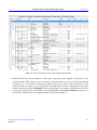
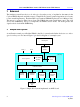
DE1 Basic Computer Contents
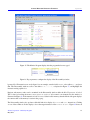
A block diagram of the DE1 Basic Computer is shown in Figure 1. Its main components include the Altera Nios II
processor, memory for program and data storage, parallel ports connected to switches and lights, a timer module,
and a serial port. As shown in the figure, the processor and its interfaces to I/O devices are implemented inside the
R II FPGA chip on the DE1 board. Each of the components shown in Figure 1 is described below.
Cyclone°
2.1
Nios II Processor
R II processor is a 32-bit CPU that can be instantiated in an Altera FPGA chip. Three versions of
The Altera Nios°
the Nios II processor are available, designated economy (/e), standard (/s), and fast (/f). The DE1 Basic Computer
includes the Nios II/e version, which has an appropriate feature set for use in introductory experiments.
An overview of the Nios II processor can be found in the document Introduction to the Altera Nios II Processor,
which is provided in the University Program section of Altera’s web site. An easy way to begin working with the
DE1 Basic Computer and the Nios II processor is to make use of a utility called the Altera Monitor Program. This
utility provides an easy way to assemble and compile Nios II programs on the DE1 Basic Computer that are written
in either assembly language or the C programming language. The Monitor Program, which can be downloaded
from Altera’s web site, is an application program that runs on the host computer connected to the DE1 board. The
Monitor Program can be used to control the execution of code on Nios II, list (and edit) the contents of processor
registers, display/edit the contents of memory on the DE1 board, and similar operations. The Monitor Program
includes the DE1 Basic Computer as a predesigned system that can be downloaded onto the DE1 board, as well as
several sample programs in assembly language and C that show how to use various peripheral devices in the DE1
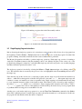
Basic Computer. Some images that show how the DE1 Basic Computer is integrated with the Monitor Program are
described in section 7. An overview of the Monitor Program is available in the document Altera Monitor Program
Tutorial, which is provided in Altera’s University Program web site.
Altera Corporation - University Program
May 2013
1
BASIC C OMPUTER S YSTEM FOR THE A LTERA DE1 B OARD
For Quartus II 13.0
Host computer
(USB connection)
USB
Blaster
RS-232
chip
Altera DE1 Board
KEY0
Reset
JTAG port
Nios II processor
System
ID
Parallel
port
Interval
timer
Cyclone II
FPGA chip
Parallel
port
Slider switches 7-Segment
SW9-0
HEX3-HEX0
Serial port
On-chip
memory
Parallel
ports
Parallel
port
SRAM
controller
SDRAM
controller
Parallel
ports
LEDR9-0
LEDG7-0
Pushbuttons
KEY3-1
SRAM
chip
SDRAM
chip
Expansion
JP0, JP1
Figure 1. Block diagram of the DE1 Basic Computer.
As indicated in Figure 1, the Nios II processor can be reset by pressing KEY0 on the DE1 board. The reset mechanism
is discussed further in section 3. All of the I/O peripherals in the DE1 Basic Computer are accessible by the processor
as memory mapped devices, using the address ranges that are given in the following subsections.
2.2
Memory Components
The DE1 Basic Computer has three types of memory components: SDRAM, SRAM, and on-chip memory inside
the FPGA chip. Each type of memory is described below.
2.2.1
SDRAM
An SDRAM Controller provides a 32-bit interface to the synchronous dynamic RAM (SDRAM) chip on the DE1
board. This SDRAM chip is organized as 1M x 16 bits x 4 banks, but is accessible by the Nios II processor
using word (32-bit), halfword (16-bit), or byte operations. The SDRAM memory is mapped to the address space
0x00000000 to 0x007FFFFF.
2
Altera Corporation - University Program
May 2013
BASIC C OMPUTER S YSTEM FOR THE A LTERA DE1 B OARD
2.2.2
For Quartus II 13.0
SRAM
An SRAM Controller provides a 32-bit interface to the static RAM (SRAM) chip on the DE1 board. This SRAM
chip is organized as 256K x 16 bits, but is accessible by the Nios II processor using word (32-bit), halfword (16-bit),
or byte operations. The SRAM memory is mapped to the address space 0x08000000 to 0x0807FFFF.
2.2.3
On-Chip Memory
The DE1 Basic Computer includes an 8-Kbyte memory that is implemented in the Cyclone II FPGA chip. This
memory is organized as 2K x 32 bits, and can be accessed using either word, halfword, or byte operations. The
memory spans addresses in the range 0x09000000 to 0x09001FFF.
2.3
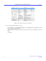
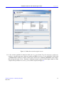
Parallel Ports
The DE1 Basic Computer includes several parallel ports that support input, output, and bidirectional transfers of data
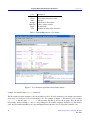
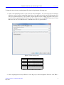
between the Nios II processor and I/O peripherals. As illustrated in Figure 2, each parallel port is assigned a Base
address and contains up to four 32-bit registers. Ports that have output capability include a writable Data register,
and ports with input capability have a readable Data register. Bidirectional parallel ports also include a Direction
register that has the same bit-width as the Data register. Each bit in the Data register can be configured as an input
by setting the corresponding bit in the Direction register to 0, or as an output by setting this bit position to 1. The
Direction register is assigned the address Base + 4.
Address
31
30
...
4
3
2
Input or output data bits
Base
1
0
Data register
Base + 4
Direction bits
Base + 8
Mask bits
Interruptmask register
Base + C
Edge bits
Edgecapture register
Direction register
Figure 2. Parallel port registers in the DE1 Basic Computer.
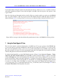
Some of the parallel ports in the DE1 Basic Computer have registers at addresses Base + 8 and Base + C, as indicated
in Figure 2. These registers are discussed in section 3.
2.3.1
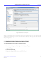
Red and Green LED Parallel Ports
The red lights LEDR9−0 and green lights LEDG7−0 on the DE1 board are each driven by an output parallel port,
as illustrated in Figure 3. The port connected to LEDR contains an 10-bit write-only Data register, which has the
address 0x10000000. The port for LEDG has a eight-bit Data register that is mapped to address 0x10000010.
These two registers can be written using word accesses, with the upper bits not used in the registers being ignored.
Altera Corporation - University Program
May 2013
3
BASIC C OMPUTER S YSTEM FOR THE A LTERA DE1 B OARD
For Quartus II 13.0
Address
0x10000000
Unused
31
10
...
9
0
LEDR9
0x10000010
Unused
31
8
7
Data register
LEDR0
...
0
Data register
LEDG7 LEDG0
Figure 3. Output parallel ports for LEDR and LEDG.
2.3.2
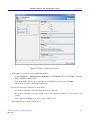
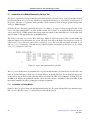
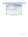
7-Segment Displays Parallel Port
There is a parallel ports connected to the 7-segment displays on the DE1 board, which comprises a 32-bit write-only
Data register. As indicated in Figure 4, the register at address 0x10000020 drives digits HEX3 to HEX0. Data
can be written into this register by using word operations. This data directly controls the segments of each display,
according to the bit locations given in Figure 4. The locations of segments 6 to 0 in each seven-segment display on
the DE1 board is illustrated on the right side of the figure.
Address
0x10000020
31 30
24
23 22
16
15 14
8
7 6
0
...
...
...
...
HEX36-0
HEX26-0
HEX16-0
HEX06-0
Data register
0
5
6
4
1
2
3
Segments
Figure 4. Bit locations for the 7-segment displays parallel ports.
2.3.3
Slider Switch Parallel Port
The SW9−0 slider switches on the DE1 board are connected to an input parallel port. As illustrated in Figure 5, this
port comprises an 10-bit read-only Data register, which is mapped to address 0x10000040.
4
Altera Corporation - University Program
May 2013
BASIC C OMPUTER S YSTEM FOR THE A LTERA DE1 B OARD
For Quartus II 13.0
Address
0x10000040
Unused
31
10
...
9
Data register
0
...
SW9
SW0
Figure 5. Data register in the slider switch parallel port.
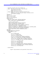
2.3.4
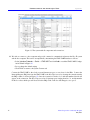
Pushbutton Parallel Port
The parallel port connected to the KEY3−1 pushbutton switches on the DE1 board comprises three 3-bit registers, as
shown in Figure 6. These registers have base addresses 0x10000050 to 0x1000005C and can be accessed using
word operations. The read-only Data register provides the values of the switches KEY3 , KEY2 and KEY1 . Bit 0 of the
data register is not used, because, as discussed in section 2.1, the corresponding switch KEY0 is reserved for use as a
reset mechanism for the DE1 Basic Computer. The other two registers shown in Figure 6, at addresses 0x10000058
and 0x1000005C, are discussed in section 3.
Address
31
30
0x10000050
...
4
Unused
3
2
KEY3-1
1
0
Data register
Unused
Unused
0x10000058
Unused
Mask bits
Interruptmask register
0x1000005C
Unused
Edge bits
Edgecapture register
Figure 6. Registers used in the pushbutton parallel port.
2.3.5
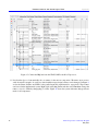
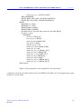
Expansion Parallel Ports
The DE1 Basic Computer includes two bidirectional parallel ports that are connected to the JP1 and JP2 expansion
headers on the DE1 board. Each of these parallel ports includes the four 32-bit registers that were described previously for Figure 2. The base addresses of the ports connected to JP1 and JP2 are 0x10000060 and 0x10000070,
respectively. Figure 7 gives a diagram of the JP1 and JP2 expansion connectors on the DE1 board, and shows how
the respective parallel port Data register bits, D 31−0 , are assigned to the pins on the connector. The figure shows that
bit D 0 of the parallel port for JP1 is assigned to the pin at the top right corner of the connector, bit D 1 is assigned
below this, and so on. Note that some of the pins on JP1 and JP2 are not usable as input/output connections, and are
therefore not used by the parallel ports. Also, only 32 of the 36 data pins that appear on each connector can be used.
Altera Corporation - University Program
May 2013
5
BASIC C OMPUTER S YSTEM FOR THE A LTERA DE1 B OARD
JP1
Pin 1
Pin 1
D0
D1
D2 D3
D4 D5
D6 D7
Unused
D8 D9
D10 D11
D12 D13
D14
D15
D16 D17
D18 D19
D20 D21
Unused
D22 D23
D24 D25
D26 D27
D28 D29
D30 D31 Pin 40
For Quartus II 13.0
JP2
D0
D1
D2 D3
D4 D5
D6 D7
Unused
D8 D9
D10 D11
D12 D13
D14
D15
D16 D17
D18 D19
D20 D21
Unused
D22 D23
D24 D25
D26 D27
D28 D29
D30 D31 Pin 40
Figure 7. Assignment of parallel port bits to pins on JP1 and JP2.
2.3.6
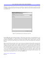
Using the Parallel Ports with Assembly Language Code and C Code
The DE1 Basic Computer provides a convenient platform for experimenting with Nios II assembly language code, or
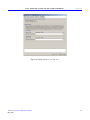
C code. A simple example of such code is provided in Figures 8 and 9. Both programs perform the same operations,
and illustrate the use of parallel ports by using either assembly language or C code.
The code in the figures displays the values of the SW switches on the red LEDs, and the pushbutton keys on the
green LEDs. It also displays a rotating pattern on 7-segment displays HEX3 . . . HEX0. This pattern is shifted to the
right by using a Nios II rotate instruction, and a delay loop is used to make the shifting slow enough to observe. The
pattern on the HEX displays can be changed to the values of the SW switches by pressing any of pushbuttons KEY3 ,
KEY2 , or KEY1 (recall from section 2.1 that KEY0 causes a reset of the DE1 Basic Computer). When a pushbutton
key is pressed, the program waits in a loop until the key is released.
The source code files shown in Figures 8 and 9 are distributed as part of the Altera Monitor Program. The files can
be found under the heading sample programs, and are identified by the name Getting Started.
6
Altera Corporation - University Program
May 2013
BASIC C OMPUTER S YSTEM FOR THE A LTERA DE1 B OARD
For Quartus II 13.0
/********************************************************************************
* This program demonstrates the use of parallel ports in the DE1 Basic Computer:
*
1. displays the SW switch values on the red LEDR
*
2. displays the KEY[3..1] pushbutton values on the green LEDG
*
3. displays a rotating pattern on the HEX displays
*
4. if KEY[3..1] is pressed, uses the SW switches as the pattern
********************************************************************************/
.text
/* executable code follows */
.global _start
_start:
/* initialize base addresses of parallel ports */
movia
r15, 0x10000040
/* SW slider switch base address */
movia
r16, 0x10000000
/* red LED base address */
movia
r17, 0x10000050
/* pushbutton KEY base address */
movia
r18, 0x10000010
/* green LED base address */
movia
r20, 0x10000020
/* HEX3_HEX0 base address */
movia
r19, HEX_bits
ldw
r6, 0(r19)
/* load pattern for HEX displays */
DO_DISPLAY:
ldwio
r4, 0(r15)
stwio
r4, 0(r16)
ldwio
r5, 0(r17)
stwio
r5, 0(r18)
beq
r5, r0, NO_BUTTON
mov
r6, r4
WAIT:
ldwio
r5, 0(r17)
bne
r5, r0, WAIT
NO_BUTTON:
stwio
r6, 0(r20)
roli
r6, r6, 1
movia
r7, 100000
DELAY:
subi
r7, r7, 1
bne
r7, r0, DELAY
br
DO_DISPLAY
.data
HEX_bits:
.word 0x0000000F
.end
/* load input from slider switches */
/* write to red LEDs */
/* load input from pushbuttons */
/* write to green LEDs */
/* copy SW switch values onto HEX displays */
/* load input from pushbuttons */
/* wait for button release */
/* store to HEX3 ... HEX0 */
/* rotate the displayed pattern */
/* delay counter */
/* data follows */
Figure 8. An example of Nios II assembly language code that uses parallel ports.
Altera Corporation - University Program
May 2013
7
BASIC C OMPUTER S YSTEM FOR THE A LTERA DE1 B OARD
For Quartus II 13.0
/********************************************************************************
* This program demonstrates the use of parallel ports in the DE1 Basic Computer:
*
1. displays the SW switch values on the red LEDR
*
2. displays the KEY[3..1] pushbutton values on the green LEDG
*
3. displays a rotating pattern on the HEX displays
*
4. if KEY[3..1] is pressed, uses the SW switches as the pattern
********************************************************************************/
int main(void)
{
/* Declare volatile pointers to I/O registers (volatile means that IO load and store
instructions (e.g., ldwio, stwio) will be used to access these pointer locations) */
volatile int * red_LED_ptr
= (int *) 0x10000000;
// red LED address
volatile int * green_LED_ptr
= (int *) 0x10000010;
// green LED address
volatile int * HEX3_HEX0_ptr = (int *) 0x10000020;
// HEX3_HEX0 address
volatile int * SW_switch_ptr
= (int *) 0x10000040;
// SW slider switch address
volatile int * KEY_ptr
= (int *) 0x10000050;
// pushbutton KEY address
int HEX_bits = 0x0000000F;
int SW_value, KEY_value;
volatile int delay_count;
while(1)
{
SW_value = *(SW_switch_ptr);
*(red_LED_ptr) = SW_value;
KEY_value = *(KEY_ptr);
*(green_LED_ptr) = KEY_value;
if (KEY_value != 0)
{
HEX_bits = SW_value;
while (*KEY_ptr);
}
*(HEX3_HEX0_ptr) = HEX_bits;
if (HEX_bits & 0x80000000)
HEX_bits = (HEX_bits << 1) | 1;
else
HEX_bits = HEX_bits << 1;
// pattern for HEX displays
// volatile so C compile does not remove loop
// read the SW slider switch values
// light up the red LEDs
// read the pushbutton KEY values
// light up the green LEDs
// check if any KEY was pressed
// set pattern using SW values
// wait for pushbutton KEY release
// display pattern on HEX3 ... HEX0
/* rotate the pattern shown on the HEX displays */
for (delay_count = 100000; delay_count != 0; − −delay_count); // delay loop
} // end while
}
Figure 9. An example of C code that uses parallel ports.
8
Altera Corporation - University Program
May 2013
BASIC C OMPUTER S YSTEM FOR THE A LTERA DE1 B OARD
2.4
For Quartus II 13.0
JTAG Port
The JTAG port implements a communication link between the DE1 board and its host computer. This link is
automatically used by the Quartus II software to transfer FPGA programming files into the DE1 board, and by
the Altera Monitor Program. The JTAG port also includes a UART, which can be used to transfer character data
between the host computer and programs that are executing on the Nios II processor. If the Altera Monitor Program
is used on the host computer, then this character data is sent and received through its Terminal Window. The Nios II
programming interface of the JTAG UART consists of two 32-bit registers, as shown in Figure 10. The register
mapped to address 0x10001000 is called the Data register and the register mapped to address 0x10001004 is
called the Control register.
Address
31
...
0x10001000
RAVAIL
0x10001004
WSPACE
16
14 . . . 11 10
15
RVALID
Unused
9
8
7 ... 1
Unused
AC WI RI
0
DATA
WE RE
Data register
Control register
Figure 10. JTAG UART registers.
When character data from the host computer is received by the JTAG UART it is stored in a 64-character FIFO.
The number of characters currently stored in this FIFO is indicated in the field RAVAIL, which are bits 31−16 of the
Data register. If the receive FIFO overflows, then additional data is lost. When data is present in the receive FIFO,
then the value of RAVAIL will be greater than 0 and the value of bit 15, RVALID, will be 1. Reading the character
at the head of the FIFO, which is provided in bits 7 − 0, decrements the value of RAVAIL by one and returns this
decremented value as part of the read operation. If no data is present in the receive FIFO, then RVALID will be set
to 0 and the data in bits 7 − 0 is undefined.
The JTAG UART also includes a 64-character FIFO that stores data waiting to be transmitted to the host computer.
Character data is loaded into this FIFO by performing a write to bits 7−0 of the Data register in Figure 10. Note
that writing into this register has no effect on received data. The amount of space, WSPACE, currently available in
the transmit FIFO is provided in bits 31−16 of the Control register. If the transmit FIFO is full, then any characters
written to the Data register will be lost.
Bit 10 in the Control register, called AC, has the value 1 if the JTAG UART has been accessed by the host computer.
This bit can be used to check if a working connection to the host computer has been established. The AC bit can be
cleared to 0 by writing a 1 into it.
The Control register bits RE, WE, RI, and WI are described in section 3.
2.4.1
Using the JTAG UART with Assembly Language Code and C Code
Figures 11 and 12 give simple examples of assembly language and C code, respectively, that use the JTAG UART.
Both versions of the code perform the same function, which is to first send an ASCII string to the JTAG UART, and
then enter an endless loop. In the loop, the code reads character data that has been received by the JTAG UART,
and echoes this data back to the UART for transmission. If the program is executed by using the Altera Monitor
Altera Corporation - University Program
May 2013
9
BASIC C OMPUTER S YSTEM FOR THE A LTERA DE1 B OARD
For Quartus II 13.0
Program, then any keyboard character that is typed into the Terminal Window of the Monitor Program will be echoed
back, causing the character to appear in the Terminal Window.
The source code files shown in Figures 11 and 12 are made available as part of the Altera Monitor Program. The
files can be found under the heading sample programs, and are identified by the name JTAG UART.
/********************************************************************************
* This program demonstrates use of the JTAG UART port in the DE1 Basic Computer
*
* It performs the following:
*
1. sends a text string to the JTAG UART
*
2. reads character data from the JTAG UART
*
3. echos the character data back to the JTAG UART
********************************************************************************/
.text
/* executable code follows */
.global
_start
_start:
/* set up stack pointer */
movia
sp, 0x007FFFFC
/* stack starts from highest memory address in SDRAM */
movia
r6, 0x10001000
/* print a text string */
movia
r8, TEXT_STRING
LOOP:
ldb
r5, 0(r8)
beq
r5, zero, GET_JTAG
call
PUT_JTAG
addi
r8, r8, 1
br
LOOP
/* read and echo characters */
GET_JTAG:
ldwio
r4, 0(r6)
andi
r8, r4, 0x8000
beq
r8, r0, GET_JTAG
andi
r5, r4, 0x00ff
call
br
.end
PUT_JTAG
GET_JTAG
/* JTAG UART base address */
/* string is null-terminated */
/* read the JTAG UART data register */
/* check if there is new data */
/* if no data, wait */
/* the data is in the least significant byte */
/* echo character */
Figure 11. An example of assembly language code that uses the JTAG UART (Part a).
10
Altera Corporation - University Program
May 2013
BASIC C OMPUTER S YSTEM FOR THE A LTERA DE1 B OARD
For Quartus II 13.0
/********************************************************************************
* Subroutine to send a character to the JTAG UART
*
r5 = character to send
*
r6 = JTAG UART base address
********************************************************************************/
.global
PUT_JTAG
PUT_JTAG:
/* save any modified registers */
subi
sp, sp, 4
/* reserve space on the stack */
stw
r4, 0(sp)
/* save register */
ldwio
andhi
beq
stwio
r4, 4(r6)
r4, r4, 0xffff
r4, r0, END_PUT
r5, 0(r6)
/* read the JTAG UART Control register */
/* check for write space */
/* if no space, ignore the character */
/* send the character */
END_PUT:
/* restore registers */
ldw
r4, 0(sp)
addi
sp, sp, 4
ret
.data
/* data follows */
TEXT_STRING:
.asciz "\nJTAG UART example code\n> "
.end
Figure 11. An example of assembly language code that uses the JTAG UART (Part b).
Altera Corporation - University Program
May 2013
11
BASIC C OMPUTER S YSTEM FOR THE A LTERA DE1 B OARD
void put_jtag(volatile int *, char);
For Quartus II 13.0
// function prototype
/********************************************************************************
* This program demonstrates use of the JTAG UART port in the DE1 Basic Computer
*
* It performs the following:
*
1. sends a text string to the JTAG UART
*
2. reads character data from the JTAG UART
*
3. echos the character data back to the JTAG UART
********************************************************************************/
int main(void)
{
/* Declare volatile pointers to I/O registers (volatile means that IO load and store
instructions (e.g., ldwio, stwio) will be used to access these pointer locations) */
volatile int * JTAG_UART_ptr = (int *) 0x10001000;
// JTAG UART address
int data, i;
char text_string[] = "\nJTAG UART example code\n> \0";
for (i = 0; text_string[i] != 0; ++i)
put_jtag (JTAG_UART_ptr, text_string[i]);
// print a text string
/* read and echo characters */
while(1)
{
data = *(JTAG_UART_ptr);
// read the JTAG_UART data register
if (data & 0x00008000)
// check RVALID to see if there is new data
{
data = data & 0x000000FF;
// the data is in the least significant byte
/* echo the character */
put_jtag (JTAG_UART_ptr, (char) data & 0xFF );
}
}
}
/********************************************************************************
* Subroutine to send a character to the JTAG UART
********************************************************************************/
void put_jtag( volatile int * JTAG_UART_ptr, char c )
{
int control;
control = *(JTAG_UART_ptr + 1);
// read the JTAG_UART Control register
if (control & 0xFFFF0000)
// if space, then echo character, else ignore
*(JTAG_UART_ptr) = c;
}
Figure 12. An example of C code that uses the JTAG UART.
12
Altera Corporation - University Program
May 2013
BASIC C OMPUTER S YSTEM FOR THE A LTERA DE1 B OARD
2.5
For Quartus II 13.0
Serial Port
The serial port in the DE1 Basic Computer implements a UART that is connected to an RS232 chip on the DE1
board. This UART is configured for 8-bit data, one stop bit, odd parity, and operates at a baud rate of 115,200.
The serial port’s programming interface consists of two 32-bit registers, as illustrated in Figure 13. The register
at address 0x10001010 is referred to as the Data register, and the register at address 0x10001014 is called the
Control register.
Address
31
...
0x10001010
RAVAIL
0x10001014
WSPACE
16
15
14 . . . 10 9
RVALID Unused
Unused
8
7 ... 1
PE
WI RI
0
DATA
WE RE
Data register
Control register
Figure 13. Serial port UART registers.
When character data is received from the RS 232 chip it is stored in a 256-character FIFO in the UART. As illustrated
in Figure 13, the number of characters RAVAIL currently stored in this FIFO is provided in bits 31−16 of the Data
register. If the receive FIFO overflows, then additional data is lost. When the data that is present in the receive FIFO
is available for reading, then the value of bit 15, RVALID, will be 1. Reading the character at the head of the FIFO,
which is provided in bits 7 − 0, decrements the value of RAVAIL by one and returns this decremented value as part
of the read operation. If no data is available to be read from the receive FIFO, then RVALID will be set to 0 and the
data in bits 7 − 0 is undefined.
The UART also includes a 256-character FIFO that stores data waiting to be sent to the RS 232 chip. Character data
is loaded into this register by performing a write to bits 7−0 of the Data register. Writing into this register has no
effect on received data. The amount of space WSPACE currently available in the transmit FIFO is provided in bits
31−16 of the Control register, as indicated in Figure 13. If the transmit FIFO is full, then any additional characters
written to the Data register will be lost.
The Control register bits RE, WE, RI, and WI are described in section 3.
2.6
Interval Timer
The DE1 Basic Computer includes a timer that can be used to measure various time intervals. The interval timer is
loaded with a preset value, and then counts down to zero using the 50-MHz clock signal provided on the DE1 board.
The programming interface for the timer includes six 16-bit registers, as illustrated in Figure 14. The 16-bit register
at address 0x10002000 provides status information about the timer, and the register at address 0x10002004 allows
control settings to be made. The bit fields in these registers are described below:
• TO provides a timeout signal which is set to 1 by the timer when it has reached a count value of zero. The TO
bit can be reset by writing a 0 into it.
• RUN is set to 1 by the timer whenever it is currently counting. Write operations to the status halfword do not
affect the value of the RUN bit.
Altera Corporation - University Program
May 2013
13
BASIC C OMPUTER S YSTEM FOR THE A LTERA DE1 B OARD
For Quartus II 13.0
• ITO is used for generating Nios II interrupts, which are discussed in section 3.
Address
31 . . .
17
16
15
...
0x10002000
0x1000200C
2
Unused
0x10002004
0x10002008
3
Unused
Not present
(interval timer has
16-bit registers)
1
0
RUN
TO
STOP START CONT ITO
Status register
Control register
Counter start value (low)
Counter start value (high)
0x10002010
Counter snapshot (low)
0x10002014
Counter snapshot (high)
Figure 14. Interval timer registers.
• CONT affects the continuous operation of the timer. When the timer reaches a count value of zero it automatically reloads the specified starting count value. If CONT is set to 1, then the timer will continue counting
down automatically. But if CONT = 0, then the timer will stop after it has reached a count value of 0.
• (START/STOP) can be used to commence/suspend the operation of the timer by writing a 1 into the respective
bit.
The two 16-bit registers at addresses 0x10002008 and 0x1000200C allow the period of the timer to be changed
by setting the starting count value. The default setting provided in the DE1 Basic Computer gives a timer period
of 125 msec. To achieve this period, the starting value of the count is 50 MHz × 125 msec = 6.25 × 10⁶ . It is
possible to capture a snapshot of the counter value at any time by performing a write to address 0x10002010. This
write operation causes the current 32-bit counter value to be stored into the two 16-bit timer registers at addresses
0x10002010 and 0x10002014. These registers can then be read to obtain the count value.
2.7
System ID
The system ID module provides a unique value that identifies the DE1 Basic Computer system. The host computer
connected to the DE1 board can query the system ID module by performing a read operation through the JTAG port.
The host computer can then check the value of the returned identifier to confirm that the DE1 Basic Computer has
been properly downloaded onto the DE1 board. This process allows debugging tools on the host computer, such as
the Altera Monitor Program, to verify that the DE1 board contains the required computer system before attempting
to execute code that has been compiled for this system.
14
Altera Corporation - University Program
May 2013
BASIC C OMPUTER S YSTEM FOR THE A LTERA DE1 B OARD
3
For Quartus II 13.0
Exceptions and Interrupts
The reset address of the Nios II processor in the DE1 Basic Computer is set to 0x00000000. The address used
for all other general exceptions, such as divide by zero, and hardware IRQ interrupts is 0x00000020. Since the
Nios II processor uses the same address for general exceptions and hardware IRQ interrupts, the Exception Handler
software must determine the source of the exception by examining the appropriate processor status register. Table 1
gives the assignment of IRQ numbers to each of the I/O peripherals in the DE1 Basic Computer.
I/O Peripheral
Interval timer
Pushbutton switch parallel port
JTAG port
Serial port
JP1 Expansion parallel port
JP2 Expansion parallel port
IRQ #
0
1
8
10
11
12
Table 1. Hardware IRQ interrupt assignment for the DE1 Basic Computer.
3.1
Interrupts from Parallel Ports
Parallel port registers in the DE1 Basic Computer were illustrated in Figure 2, which is reproduced as Figure 15.
As the figure shows, parallel ports that support interrupts include two related registers at the addresses Base + 8 and
Base + C. The Interruptmask register, which has the address Base + 8, specifies whether or not an interrupt signal
should be sent to the Nios II processor when the data present at an input port changes value. Setting a bit location in
this register to 1 allows interrupts to be generated, while setting the bit to 0 prevents interrupts. Finally, the parallel
port may contain an Edgecapture register at address Base + C. Each bit in this register has the value 1 if the corresponding bit location in the parallel port has changed its value from 0 to 1 since it was last read. Performing a write
operation to the Edgecapture register sets all bits in the register to 0, and clears any associated Nios II interrupts.
Address
31
30
...
4
3
2
Input or output data bits
Base
1
0
Data register
Base + 4
Direction bits
Base + 8
Mask bits
Interruptmask register
Base + C
Edge bits
Edgecapture register
Direction register
Figure 15. Registers used for interrupts from the parallel ports.
Altera Corporation - University Program
May 2013
15
BASIC C OMPUTER S YSTEM FOR THE A LTERA DE1 B OARD
3.1.1
For Quartus II 13.0
Interrupts from the Pushbutton Switches
Figure 6, reproduced as Figure 16, shows the registers associated with the pushbutton parallel port. The Interruptmask register allows processor interrupts to be generated when a key is pressed. Each bit in the Edgecapture register
is set to 1 by the parallel port when the corresponding key is pressed. The Nios II processor can read this register
to determine which key has been pressed, in addition to receiving an interrupt request if the corresponding bit in
the interrupt mask register is set to 1. Writing any value to the Edgecapture register deasserts the Nios II interrupt
request and sets all bits of the Edgecapture register to zero.
Address
31
30
0x10000050
...
4
Unused
3
2
1
0
Data register
KEY3-1
Unused
Unused
0x10000058
Unused
Mask bits
Interruptmask register
0x1000005C
Unused
Edge bits
Edgecapture register
Figure 16. Registers used for interrupts from the pushbutton parallel port.
3.2
Interrupts from the JTAG UART
Figure 10, reproduced as Figure 17, shows the Data and Control registers of the JTAG UART. As we said in section
2.4, RAVAIL in the data register gives the number of characters that are stored in the receive FIFO, and WSPACE
gives the amount of unused space that is available in the transmit FIFO. The RE and WE bits in Figure 17 are used to
enable processor interrupts associated with the receive and transmit FIFOs. When enabled, interrupts are generated
when RAVAIL for the receive FIFO, or WSPACE for the transmit FIFO, exceeds 7. Pending interrupts are indicated
in the Control register’s RI and WI bits, and can be cleared by writing or reading data to/from the JTAG UART.
Address
31
...
0x10001000
RAVAIL
0x10001004
WSPACE
14 . . . 11 10
15
16
RVALID
Unused
9
8
Unused
AC WI RI
7 ... 1
0
DATA
WE RE
Data register
Control register
Figure 17. Interrupt bits in the JTAG UART registers.
3.3
Interrupts from the serial port UART
We introduced the Data and Control registers associated with the serial port UART in Figure 13, in section 2.5.
The RE and WE bits in the Control register in Figure 13 are used to enable processor interrupts associated with the
receive and transmit FIFOs. When enabled, interrupts are generated when RAVAIL for the receive FIFO, or WSPACE
for the transmit FIFO, exceeds 31. Pending interrupts are indicated in the Control register’s RI and WI bits, and can
be cleared by writing or reading data to/from the UART.
16
Altera Corporation - University Program
May 2013
BASIC C OMPUTER S YSTEM FOR THE A LTERA DE1 B OARD
3.4
For Quartus II 13.0
Interrupts from the Interval Timer
Figure 14, in section 2.6, shows six registers that are associated with the interval timer. As we said in section 2.6,
the bit b0 (TO) is set to 1 when the timer reaches a count value of 0. It is possible to generate an interrupt when this
occurs, by using the bit b16 (ITO). Setting the bit ITO to 1 allows an interrupt request to be generated whenever TO
becomes 1. After an interrupt occurs, it can be cleared by writing any value to the register that contains the bit TO.
3.5
Using Interrupts with Assembly Language Code
An example of assembly language code for the DE1 Basic Computer that uses interrupts is shown in Figure 18.
When this code is executed on the DE1 board it displays a rotating pattern on the HEX 7-segment displays. The
pattern rotates to the right if pushbutton KEY1 is pressed, and to the left if KEY2 is pressed. Pressing KEY3 causes
the pattern to be set using the SW switch values. Two types of interrupts are used in the code. The HEX displays
are controlled by an interrupt service routine for the interval timer, and another interrupt service routine is used to
handle the pushbutton keys. The speed at which the HEX displays are rotated is set in the main program, by using a
counter value in the interval timer that causes an interrupt to occur every 33 msec.
.equ
KEY1, 0
.equ
KEY2, 1
/********************************************************************************
* This program demonstrates use of interrupts in the DE1 Basic Computer. It first starts the
* interval timer with 33 msec timeouts, and then enables interrupts from the interval timer
* and pushbutton KEYs
*
* The interrupt service routine for the interval timer displays a pattern on the HEX displays, and
* shifts this pattern either left or right. The shifting direction is set in the pushbutton
* interrupt service routine, as follows:
*
KEY[1]: shifts the displayed pattern to the right
*
KEY[2]: shifts the displayed pattern to the left
*
KEY[3]: changes the pattern using the settings on the SW switches
********************************************************************************/
.text
/* executable code follows */
.global
_start
_start:
/* set up stack pointer */
movia
sp, 0x007FFFFC
/* stack starts from highest memory address in SDRAM */
movia
r16, 0x10002000
/* internal timer base address */
/* set the interval timer period for scrolling the HEX displays */
movia
r12, 0x190000
/* 1/(50 MHz) × (0x190000) = 33 msec */
sthio
r12, 8(r16)
/* store the low halfword of counter start value */
srli
r12, r12, 16
sthio
r12, 0xC(r16)
/* high halfword of counter start value */
Figure 18. An example of assembly language code that uses interrupts (Part a).
Altera Corporation - University Program
May 2013
17
BASIC C OMPUTER S YSTEM FOR THE A LTERA DE1 B OARD
For Quartus II 13.0
/* start interval timer, enable its interrupts */
movi
r15, 0b0111
/* START = 1, CONT = 1, ITO = 1 */
sthio
r15, 4(r16)
/* write to the pushbutton port interrupt mask register */
movia
r15, 0x10000050
/* pushbutton key base address */
movi
r7, 0b01110
/* set 3 interrupt mask bits (bit 0 is Nios II reset) */
stwio
r7, 8(r15)
/* interrupt mask register is (base + 8) */
/* enable Nios II processor interrupts */
movi
r7, 0b011
/* set interrupt mask bits for levels 0 (interval */
wrctl
ienable, r7
/* timer) and level 1 (pushbuttons) */
movi
r7, 1
wrctl
status, r7
/* turn on Nios II interrupt processing */
IDLE:
br
IDLE
/* main program simply idles */
.data
/* The two global variables used by the interrupt service routines for the interval timer and the
* pushbutton keys are declared below */
.global
PATTERN:
.word
PATTERN
0x0000000F
.global
KEY_PRESSED
KEY_PRESSED:
.word
KEY2
/* pattern to show on the HEX displays */
/* stores code representing pushbutton key pressed */
.end
Figure 18. An example of assembly language code that uses interrupts (Part b).
The reset and exception handlers for the main program in Figure 18 are given in Figure 19. The reset handler simply
jumps to the _start symbol in the main program. The exception handler first checks if the exception that has occurred
is an external interrupt or an internal one. In the case of an internal exception, such as an illegal instruction opcode
or a trap instruction, the handler simply exits, because it does not handle these cases. For external exceptions, it
calls either the interval timer interrupt service routine, for a level 0 interrupt, or the pushbutton key interrupt service
routine for level 1. These routines are shown in Figures 20 and 21, respectively.
18
Altera Corporation - University Program
May 2013
BASIC C OMPUTER S YSTEM FOR THE A LTERA DE1 B OARD
For Quartus II 13.0
/********************************************************************************
* RESET SECTION
* The Monitor Program automatically places the ".reset" section at the reset location
* specified in the CPU settings in Qsys.
* Note: "ax" is REQUIRED to designate the section as allocatable and executable.
*/
.section .reset, "ax"
movia
r2, _start
jmp
r2
/* branch to main program */
/********************************************************************************
* EXCEPTIONS SECTION
* The Monitor Program automatically places the ".exceptions" section at the
* exception location specified in the CPU settings in Qsys.
* Note: "ax" is REQUIRED to designate the section as allocatable and executable.
*/
.section .exceptions, "ax"
.global
EXCEPTION_HANDLER
EXCEPTION_HANDLER:
subi
sp, sp, 16
/* make room on the stack */
stw
et, 0(sp)
rdctl
beq
et, ctl4
et, r0, SKIP_EA_DEC
subi
ea, ea, 4
SKIP_EA_DEC:
stw
ea, 4(sp)
stw
ra, 8(sp)
stw
r22, 12(sp)
rdctl
bne
NOT_EI:
br
/* interrupt is not external */
/* must decrement ea by one instruction */
/* for external interrupts, so that the */
/* interrupted instruction will be run after eret */
/* save all used registers on the Stack */
/* needed if call inst is used */
et, ctl4
et, r0, CHECK_LEVEL_0
/* exception is an external interrupt */
END_ISR
/* exception must be unimplemented instruction or TRAP */
/* instruction. This code does not handle those cases */
Figure 19. Reset and exception handler assembly language code (Part a ).
Altera Corporation - University Program
May 2013
19
BASIC C OMPUTER S YSTEM FOR THE A LTERA DE1 B OARD
For Quartus II 13.0
CHECK_LEVEL_0:
/* interval timer is interrupt level 0 */
andi
r22, et, 0b1
beq
r22, r0, CHECK_LEVEL_1
call
INTERVAL_TIMER_ISR
br
END_ISR
CHECK_LEVEL_1:
andi
r22, et, 0b10
beq
r22, r0, END_ISR
call
PUSHBUTTON_ISR
END_ISR:
ldw
ldw
ldw
ldw
addi
et, 0(sp)
ea, 4(sp)
ra, 8(sp)
r22, 12(sp)
sp, sp, 16
/* pushbutton port is interrupt level 1 */
/* other interrupt levels are not handled in this code */
/* restore all used register to previous values */
/* needed if call inst is used */
eret
.end
Figure 19. Reset and exception handler assembly language code (Part b).
.include
"key_codes.s"
/* includes EQU for KEY1, KEY2 */
.extern
PATTERN
/* externally defined variables */
.extern
KEY_PRESSED
/********************************************************************************
* Interval timer interrupt service routine
*
* Shifts a PATTERN being displayed on the HEX displays. The shift direction
* is determined by the external variable KEY_PRESSED.
*
********************************************************************************/
.global
INTERVAL_TIMER_ISR
INTERVAL_TIMER_ISR:
subi
sp, sp, 36
/* reserve space on the stack */
stw
ra, 0(sp)
stw
r4, 4(sp)
stw
r5, 8(sp)
stw
r6, 12(sp)
Figure 20. Interrupt service routine for the interval timer (Part a ).
20
Altera Corporation - University Program
May 2013
BASIC C OMPUTER S YSTEM FOR THE A LTERA DE1 B OARD
stw
stw
stw
stw
stw
r8, 16(sp)
r10, 20(sp)
r20, 24(sp)
r21, 28(sp)
r22, 32(sp)
movia
sthio
r10, 0x10002000
r0, 0(r10)
/* interval timer base address */
/* clear the interrupt */
movia
addi
movia
movia
r20, 0x10000020
r5, r0, 1
r21, PATTERN
r22, KEY_PRESSED
/* HEX3_HEX0 base address */
/* set r5 to the constant value 1 */
/* set up a pointer to the pattern for HEX displays */
/* set up a pointer to the key pressed */
ldw
stwio
r6, 0(r21)
r6, 0(r20)
/* load pattern for HEX displays */
/* store to HEX3 ... HEX0 */
ldw
movi
beq
rol
br
LEFT:
ror
For Quartus II 13.0
r4, 0(r22)
/* check which key has been pressed */
r8, KEY1
/* code to check for KEY1 */
r4, r8, LEFT
/* for KEY1 pressed, shift right */
r6, r6, r5
/* else (for KEY2) pressed, shift left */
END_INTERVAL_TIMER_ISR
r6, r6, r5
END_INTERVAL_TIMER_ISR:
stw
r6, 0(r21)
ldw
ra, 0(sp)
ldw
r4, 4(sp)
ldw
r5, 8(sp)
ldw
r6, 12(sp)
ldw
r8, 16(sp)
ldw
r10, 20(sp)
ldw
r20, 24(sp)
ldw
r21, 28(sp)
ldw
r22, 32(sp)
addi
sp, sp, 36
ret
.end
/* rotate the displayed pattern right */
/* store HEX display pattern */
/* Restore all used register to previous */
/* release the reserved space on the stack */
Figure 20. Interrupt service routine for the interval timer (Part b).
Altera Corporation - University Program
May 2013
21
BASIC C OMPUTER S YSTEM FOR THE A LTERA DE1 B OARD
For Quartus II 13.0
.include
"key_codes.s"
/* includes EQU for KEY1, KEY2 */
.extern
PATTERN
/* externally defined variables */
.extern
KEY_PRESSED
/********************************************************************************
* Pushbutton - Interrupt Service Routine
*
* This routine checks which KEY has been pressed. If it is KEY1 or KEY2, it writes this value
* to the global variable KEY_PRESSED. If it is KEY3 then it loads the SW switch values and
* stores in the variable PATTERN
********************************************************************************/
.global
PUSHBUTTON_ISR
PUSHBUTTON_ISR:
subi
sp, sp, 20
/* reserve space on the stack */
stw
ra, 0(sp)
stw
r10, 4(sp)
stw
r11, 8(sp)
stw
r12, 12(sp)
stw
r13, 16(sp)
movia
ldwio
stwio
r10, 0x10000050
r11, 0xC(r10)
r0, 0xC(r10)
/* base address of pushbutton KEY parallel port */
/* read edge capture register */
/* clear the interrupt */
movia
r10, KEY_PRESSED /* global variable to return the result */
CHECK_KEY1:
andi
r13, r11, 0b0010
/* check KEY1 */
beq
r13, zero, CHECK_KEY2
movi
r12, KEY1
stw
r12, 0(r10)
/* return KEY1 value */
br
END_PUSHBUTTON_ISR
CHECK_KEY2:
andi
r13, r11, 0b0100
/* check KEY2 */
beq
r13, zero, DO_KEY3
movi
r12, KEY2
stw
r12, 0(r10)
/* return KEY2 value */
br
END_PUSHBUTTON_ISR
DO_KEY3:
movia
ldwio
movia
stw
r13, 0x10000040
r11, 0(r13)
r13, PATTERN
r11, 0(r13)
/* SW slider switch base address */
/* load slider switches */
/* address of pattern for HEX displays */
/* save new pattern */
Figure 21. Interrupt service routine for the pushbutton keys (Part a ).
22
Altera Corporation - University Program
May 2013
BASIC C OMPUTER S YSTEM FOR THE A LTERA DE1 B OARD
END_PUSHBUTTON_ISR:
ldw
ra, 0(sp)
ldw
r10, 4(sp)
ldw
r11, 8(sp)
ldw
r12, 12(sp)
ldw
r13, 16(sp)
addi
sp, sp, 20
For Quartus II 13.0
/* Restore all used register to previous values */
ret
.end
Figure 21. Interrupt service routine for the pushbutton keys (Part b).
3.6
Using Interrupts with C Language Code
An example of C language code for the DE1 Basic Computer that uses interrupts is shown in Figure 22. This code
performs exactly the same operations as the code described in Figure 18.
To enable interrupts the code in Figure 22 uses macros that provide access to the Nios II status and control registers.
A collection of such macros, which can be used in any C program, are provided in Figure 23.
The reset and exception handlers for the main program in Figure 22 are given in Figure 24. The function called
the_reset provides a simple reset mechanism by performing a branch to the main program. The function named
the_exception represents a general exception handler that can be used with any C program. It includes assembly
language code to check if the exception is caused by an external interrupt, and, if so, calls a C language routine
named interrupt_handler. This routine can then perform whatever action is needed for the specific application.
In Figure 24, the interrupt_handler code first determines which exception has occurred, by using a macro from
Figure 23 that reads the content of the Nios II interrupt pending register. The interrupt service routine that is
invoked for the interval timer is shown in 25, and the interrupt service routine for the pushbutton switches appears
in Figure 26.
The source code files shown in Figure 18 to Figure 26 are distributed as part of the Altera Monitor Program. The
files can be found under the heading sample programs, and are identified by the name Interrupt Example.
Altera Corporation - University Program
May 2013
23
BASIC C OMPUTER S YSTEM FOR THE A LTERA DE1 B OARD
#include "nios2_ctrl_reg_macros.h"
#include "key_codes.h"
For Quartus II 13.0
// defines values for KEY1, KEY2
/* key_pressed and pattern are written by interrupt service routines; we have to declare
* these as volatile to avoid the compiler caching their values in registers */
volatile int key_pressed = KEY2;
// shows which key was last pressed
volatile int pattern = 0x0000000F;
// pattern for HEX displays
/********************************************************************************
* This program demonstrates use of interrupts in the DE1 Basic Computer. It first starts the
* interval timer with 33 msec timeouts, and then enables interrupts from the interval timer
* and pushbutton KEYs
*
* The interrupt service routine for the interval timer displays a pattern on the HEX displays, and
* shifts this pattern either left or right. The shifting direction is set in the pushbutton
* interrupt service routine, as follows:
*
KEY[1]: shifts the displayed pattern to the right
*
KEY[2]: shifts the displayed pattern to the left
*
KEY[3]: changes the pattern using the settings on the SW switches
********************************************************************************/
int main(void)
{
/* Declare volatile pointers to I/O registers (volatile means that IO load and store instructions
* will be used to access these pointer locations instead of regular memory loads and stores) */
volatile int * interval_timer_ptr = (int *) 0x10002000; // interval timer base address
volatile int * KEY_ptr = (int *) 0x10000050;
// pushbutton KEY address
/* set the interval timer period for scrolling the HEX displays */
int counter = 0x190000;
// 1/(50 MHz) × (0x190000) = 33 msec
*(interval_timer_ptr + 0x2) = (counter & 0xFFFF);
*(interval_timer_ptr + 0x3) = (counter >> 16) & 0xFFFF;
/* start interval timer, enable its interrupts */
*(interval_timer_ptr + 1) = 0x7;
// STOP = 0, START = 1, CONT = 1, ITO = 1
*(KEY_ptr + 2) = 0xE;
/* write to the pushbutton interrupt mask register, and
* set 3 mask bits to 1 (bit 0 is Nios II reset) */
NIOS2_WRITE_IENABLE( 0x3 );
NIOS2_WRITE_STATUS( 1 );
/* set interrupt mask bits for levels 0 (interval timer)
* and level 1 (pushbuttons) */
// enable Nios II interrupts
while(1);
// main program simply idles
}
Figure 22. An example of C code that uses interrupts.
24
Altera Corporation - University Program
May 2013
BASIC C OMPUTER S YSTEM FOR THE A LTERA DE1 B OARD
For Quartus II 13.0
#ifndef __NIOS2_CTRL_REG_MACROS__
#define __NIOS2_CTRL_REG_MACROS__
/*****************************************************************************/
/* Macros for accessing the control registers.
*/
/*****************************************************************************/
#define NIOS2_READ_STATUS(dest) \
do { dest = __builtin_rdctl(0); } while (0)
#define NIOS2_WRITE_STATUS(src) \
do { __builtin_wrctl(0, src); } while (0)
#define NIOS2_READ_ESTATUS(dest) \
do { dest = __builtin_rdctl(1); } while (0)
#define NIOS2_READ_BSTATUS(dest) \
do { dest = __builtin_rdctl(2); } while (0)
#define NIOS2_READ_IENABLE(dest) \
do { dest = __builtin_rdctl(3); } while (0)
#define NIOS2_WRITE_IENABLE(src) \
do { __builtin_wrctl(3, src); } while (0)
#define NIOS2_READ_IPENDING(dest) \
do { dest = __builtin_rdctl(4); } while (0)
#define NIOS2_READ_CPUID(dest) \
do { dest = __builtin_rdctl(5); } while (0)
#endif
Figure 23. Macros for accessing Nios II status and control registers.
Altera Corporation - University Program
May 2013
25
BASIC C OMPUTER S YSTEM FOR THE A LTERA DE1 B OARD
For Quartus II 13.0
#include "nios2_ctrl_reg_macros.h"
/* function prototypes */
void main(void);
void interrupt_handler(void);
void interval_timer_isr(void);
void pushbutton_ISR(void);
/* global variables */
extern int key_pressed;
/* The assembly language code below handles Nios II reset processing */
void the_reset (void) __attribute__ ((section (".reset")));
void the_reset (void)
/*******************************************************************************
* Reset code; by using the section attribute with the name ".reset" we allow the linker program
* to locate this code at the proper reset vector address. This code just calls the main program
******************************************************************************/
{
asm (".set
noat");
// magic, for the C compiler
asm (".set
nobreak");
// magic, for the C compiler
asm ("movia r2, main");
// call the C language main program
asm ("jmp r2");
}
/* The assembly language code below handles Nios II exception processing. This code should not be
* modified; instead, the C language code in the function interrupt_handler() can be modified as
* needed for a given application. */
void the_exception (void) __attribute__ ((section (".exceptions")));
void the_exception (void)
/*******************************************************************************
* Exceptions code; by giving the code a section attribute with the name ".exceptions" we allow
* the linker to locate this code at the proper exceptions vector address. This code calls the
* interrupt handler and later returns from the exception.
******************************************************************************/
{
asm (".set
noat");
// magic, for the C compiler
asm (".set
nobreak");
// magic, for the C compiler
asm ( "subi sp, sp, 128");
asm ( "stw et, 96(sp)");
asm ( "rdctl et, ctl4");
asm ( "beq et, r0, SKIP_EA_DEC"); // interrupt is not external
asm ( "subi ea, ea, 4");
/* must decrement ea by one instruction for external
* interrupts, so that the instruction will be run */
Figure 24. Reset and exception handler C code (Part a ).
26
Altera Corporation - University Program
May 2013
BASIC C OMPUTER S YSTEM FOR THE A LTERA DE1 B OARD
For Quartus II 13.0
asm ( "SKIP_EA_DEC:" );
asm ( "stw r1, 4(sp)" );
// save all registers
asm ( "stw r2, 8(sp)" );
asm ( "stw r3, 12(sp)" );
asm ( "stw r4, 16(sp)" );
asm ( "stw r5, 20(sp)" );
asm ( "stw r6, 24(sp)" );
asm ( "stw r7, 28(sp)" );
asm ( "stw r8, 32(sp)" );
asm ( "stw r9, 36(sp)" );
asm ( "stw r10, 40(sp)" );
asm ( "stw r11, 44(sp)" );
asm ( "stw r12, 48(sp)" );
asm ( "stw r13, 52(sp)" );
asm ( "stw r14, 56(sp)" );
asm ( "stw r15, 60(sp)" );
asm ( "stw r16, 64(sp)" );
asm ( "stw r17, 68(sp)" );
asm ( "stw r18, 72(sp)" );
asm ( "stw r19, 76(sp)" );
asm ( "stw r20, 80(sp)" );
asm ( "stw r21, 84(sp)" );
asm ( "stw r22, 88(sp)" );
asm ( "stw r23, 92(sp)" );
asm ( "stw r25, 100(sp)" );
// r25 = bt (skip r24 = et, because it was saved above)
asm ( "stw r26, 104(sp)" );
// r26 = gp
// skip r27 because it is sp, and there is no point in saving this
asm ( "stw r28, 112(sp)" );
// r28 = fp
asm ( "stw r29, 116(sp)" );
// r29 = ea
asm ( "stw r30, 120(sp)" );
// r30 = ba
asm ( "stw r31, 124(sp)" );
// r31 = ra
asm ( "addi fp, sp, 128" );
asm ( "call
interrupt_handler" );
// call the C language interrupt handler
asm ( "ldw
asm ( "ldw
asm ( "ldw
asm ( "ldw
asm ( "ldw
asm ( "ldw
asm ( "ldw
r1, 4(sp)" );
r2, 8(sp)" );
r3, 12(sp)" );
r4, 16(sp)" );
r5, 20(sp)" );
r6, 24(sp)" );
r7, 28(sp)" );
// restore all registers
Figure 24. Reset and exception handler C language code (Part b).
Altera Corporation - University Program
May 2013
27
BASIC C OMPUTER S YSTEM FOR THE A LTERA DE1 B OARD
For Quartus II 13.0
asm ( "ldw r8, 32(sp)" );
asm ( "ldw r9, 36(sp)" );
asm ( "ldw r10, 40(sp)" );
asm ( "ldw r11, 44(sp)" );
asm ( "ldw r12, 48(sp)" );
asm ( "ldw r13, 52(sp)" );
asm ( "ldw r14, 56(sp)" );
asm ( "ldw r15, 60(sp)" );
asm ( "ldw r16, 64(sp)" );
asm ( "ldw r17, 68(sp)" );
asm ( "ldw r18, 72(sp)" );
asm ( "ldw r19, 76(sp)" );
asm ( "ldw r20, 80(sp)" );
asm ( "ldw r21, 84(sp)" );
asm ( "ldw r22, 88(sp)" );
asm ( "ldw r23, 92(sp)" );
asm ( "ldw r24, 96(sp)" );
asm ( "ldw r25, 100(sp)" );
// r25 = bt
asm ( "ldw r26, 104(sp)" );
// r26 = gp
// skip r27 because it is sp, and we did not save this on the stack
asm ( "ldw r28, 112(sp)" );
// r28 = fp
asm ( "ldw r29, 116(sp)" );
// r29 = ea
asm ( "ldw r30, 120(sp)" );
// r30 = ba
asm ( "ldw r31, 124(sp)" );
// r31 = ra
asm ( "addi sp, sp, 128" );
asm ( "eret" );
}
/********************************************************************************
* Interrupt Service Routine: Determines the interrupt source and calls the appropriate subroutine
*******************************************************************************/
void interrupt_handler(void)
{
int ipending;
NIOS2_READ_IPENDING(ipending);
if ( ipending & 0x1 )
// interval timer is interrupt level 0
interval_timer_isr( );
if ( ipending & 0x2 )
// pushbuttons are interrupt level 1
pushbutton_ISR( );
// else, ignore the interrupt
return;
}
Figure 24. Reset and exception handler C code (Part c).
28
Altera Corporation - University Program
May 2013
BASIC C OMPUTER S YSTEM FOR THE A LTERA DE1 B OARD
#include "key_codes.h"
For Quartus II 13.0
// defines values for KEY1, KEY2
extern volatile int key_pressed;
extern volatile int pattern;
/********************************************************************************
* Interval timer interrupt service routine
*
* Shifts a pattern being displayed on the HEX displays. The shift direction is determined
* by the external variable key_pressed.
*
********************************************************************************/
void interval_timer_isr( )
{
volatile int * interval_timer_ptr = (int *) 0x10002000;
volatile int * HEX3_HEX0_ptr = (int *) 0x10000020;
// HEX3_HEX0 address
*(interval_timer_ptr) = 0;
// clear the interrupt
*(HEX3_HEX0_ptr) = pattern;
// display pattern on HEX3 ... HEX0
/* rotate the pattern shown on the HEX displays */
if (key_pressed == KEY2)
// for KEY2 rotate left
if (pattern & 0x80000000)
pattern = (pattern << 1) | 1;
else
pattern = pattern << 1;
else if (key_pressed == KEY1)
// for KEY1 rotate right
if (pattern & 0x00000001)
pattern = (pattern >> 1) | 0x80000000;
else
pattern = (pattern >> 1) & 0x7FFFFFFF;
return;
}
Figure 25. Interrupt service routine for the interval timer.
Altera Corporation - University Program
May 2013
29
BASIC C OMPUTER S YSTEM FOR THE A LTERA DE1 B OARD
#include "key_codes.h"
For Quartus II 13.0
// defines values for KEY1, KEY2
extern volatile int key_pressed;
extern volatile int pattern;
/********************************************************************************
* Pushbutton - Interrupt Service Routine
*
* This routine checks which KEY has been pressed. If it is KEY1 or KEY2, it writes this value
* to the global variable key_pressed. If it is KEY3 then it loads the SW switch values and
* stores in the variable pattern
********************************************************************************/
void pushbutton_ISR( void )
{
volatile int * KEY_ptr = (int *) 0x10000050;
volatile int * slider_switch_ptr = (int *) 0x10000040;
int press;
press = *(KEY_ptr + 3);
*(KEY_ptr + 3) = 0;
// read the pushbutton interrupt register
// clear the interrupt
if (press & 0x2)
key_pressed = KEY1;
else if (press & 0x4)
key_pressed = KEY2;
else
pattern = *(slider_switch_ptr);
// KEY1
// KEY2
// press & 0x8, which is KEY3
// read the SW slider switch values; store in pattern
return;
}
Figure 26. Interrupt service routine for the pushbutton keys.
30
Altera Corporation - University Program
May 2013
BASIC C OMPUTER S YSTEM FOR THE A LTERA DE1 B OARD
4
For Quartus II 13.0
Modifying the DE1 Basic Computer
It is possible to modify the DE1 Basic Computer by using Altera’s Quartus II software and Qsys System Integration
tool. Tutorials that introduce this software are provided in the University Program section of Altera’s web site. To
modify the system it is first necessary to obtain all of the relevant design source code files. The DE1 Basic Computer
is available in two versions that specify the system using either Verilog HDL or VHDL. After these files have been
obtained it is also necessary to install the source code for the I/O peripherals in the system. These peripherals are
provided in the form of Qsys IP cores and are included in a package available from Altera’s University Program web
site, called the Altera University Program IP Cores
Table 2 lists the names of the Qsys IP cores that are used in this system. When the DE1 Basic Computer design files
are opened in the Quartus II software, these cores can be examined using the Qsys System Integration tool. Each
core has a number of settings that are selectable in the Qsys System Integration tool, and includes a datasheet that
provides detailed documentation.
I/O Peripheral
SDRAM
SRAM
On-chip Memory
Red LED parallel port
Green LED parallel port
7-segment displays parallel port
Expansion parallel ports
Slider switch parallel port
Pushbutton parallel port
JTAG port
Serial port
Interval timer
System ID
Qsys Core
SDRAM Controller
SRAM
On-Chip Memory (RAM or ROM)
Parallel Port
Parallel Port
Parallel Port
Parallel Port
Parallel Port
Parallel Port
JTAG UART
RS232 UART
Interval timer
System ID Peripheral
Table 2. Qsys cores used in the DE1 Basic Computer.
The steps needed to modify the system are:
1. Install the University Program IP Cores from Altera’s University Program web site
2. Copy the design source files for the DE1 Basic Computer from the University Program web site. These files
can be found in the Design Examples section of the web site
3. Open the DE1_Basic_Computer.qpf project in the Quartus II software
4. Open the Qsys System Integration tool in the Quartus II software, and modify the system as desired
5. Generate the modified system by using the Qsys System Integration tool
6. It may be necessary to modify the Verilog or VHDL code in the top-level module, DE1_Basic_System.v/vhd,
if any I/O peripherals have been added or removed from the system
Altera Corporation - University Program
May 2013
31
BASIC C OMPUTER S YSTEM FOR THE A LTERA DE1 B OARD
For Quartus II 13.0
7. Compile the project in the Quartus II software
8. Download the modified system into the DE1 board
5
Making the System the Default Configuration
The DE1 Basic Computer can be loaded into the nonvolatile FPGA configuration memory on the DE1 board, so
that it becomes the default system whenever the board is powered on. Instructions for configuring the DE1 board
in this manner can be found in the tutorial Introduction to the Quartus II Software, which is available from Altera’s
University Program.
6
Memory Layout
Table 3 summarizes the memory map used in the DE1 Basic Computer.
Base Address
0x00000000
0x08000000
0x09000000
0x10000000
0x10000010
0x10000020
0x10000040
0x10000050
0x10000060
0x10000070
0x10001000
0x10001010
0x10002000
0x10002020
End Address
0x007FFFFF
0x0807FFFF
0x09001FFF
0x1000000F
0x1000001F
0x1000002F
0x1000004F
0x1000005F
0x1000006F
0x1000007F
0x10001007
0x10001017
0x1000201F
0x10002027
I/O Peripheral
SDRAM
SRAM
On-chip Memory
Red LED parallel port
Green LED parallel port
7-segment HEX3−HEX0 displays parallel port
Slider switch parallel port
Pushbutton parallel port
JP1 Expansion parallel port
JP2 Expansion parallel port
JTAG port
Serial port
Interval timer
System ID
Table 3. Memory layout used in the DE1 Basic Computer.
7
Altera Monitor Program Integration
As we mentioned earlier, the DE1 Basic Computer system, and the sample programs described in this document, are
made available as part of the Altera Monitor Program. Figures 27 to 30 show a series of windows that are used in the
Monitor Program to create a new project. In the first screen, shown in Figure 27, the user specifies a file system folder
where the project will be stored, and gives the project a name. Pressing Next opens the window in Figure 28. Here,
the user can select the DE1 Basic Computer as a predesigned system. The Monitor Program then fills in the relevant
information in the System details box, which includes the files called nios_system.ptf and DE1_Basic_Computer.sof.
The first of these files specifies to the Monitor Program information about the components that are available in the
32
Altera Corporation - University Program
May 2013
BASIC C OMPUTER S YSTEM FOR THE A LTERA DE1 B OARD
For Quartus II 13.0
DE1 Basic Computer, such as the type of processor and memory components, and the address map. The second file
is an FPGA programming bitstream for the DE1 Basic Computer, which can downloaded by the Monitor Program
into the DE1 board.
Figure 27. Specifying the project folder and project name.
Pressing Next again opens the window in Figure 29. Here the user selects the type of program that will be used,
such as Assembly language, or C. Then, the check box shown in the figure can be used to display the list of sample
programs for the DE1 Basic Computer that are described in this document. When a sample program is selected in
this list, its source files, and other settings, can be copied into the project folder in subsequent screens of the Monitor
Program.
Figure 30 gives the final screen that is used to create a new project in the Monitor Program. This screen shows the
addresses of the reset and exception vectors for the system being used (the reset vector address in the DE1 Basic
Computer is 0, and the exception address is 0x20), and allows the user to specify the type of memory and offset
address that should be used for the .text and .data sections of the user’s program. In cases where the reset vector can
be set to the start of the user’s program, and no interrupts are being used, the offset addresses for the .text and .data
sections would normally be left at 0. However, when interrupts are used, it is necessary to specify a value for the
.text and .data sections such that enough space is available in the memory before the start of these sections to hold
the executable code of the interrupt service routine. In the example shown in the figure, which corresponds to the
sample program using interrupts in section 3, the offset of 0x400 is used.
Altera Corporation - University Program
May 2013
33
BASIC C OMPUTER S YSTEM FOR THE A LTERA DE1 B OARD
For Quartus II 13.0
Figure 28. Specifying the Nios II system.
Figure 29. Selecting sample programs.
34
Altera Corporation - University Program
May 2013
BASIC C OMPUTER S YSTEM FOR THE A LTERA DE1 B OARD
For Quartus II 13.0
Figure 30. Setting offsets for .text and .data.
Altera Corporation - University Program
May 2013
35
Altera Monitor Program
Tutorial
For Quartus II 13.0
1
Introduction
This tutorial presents an introduction to the Altera Monitor Program, which can be used to compile, assemble, download and debug programs for Altera’s Nios II processor. The tutorial gives step-by-step instructions that illustrate
the features of the Monitor Program.
The Monitor Program is a software application which runs on a host PC, and communicates with a Nios II hardware
system on an FPGA board. The Monitor Program is compatible with Microsoft Windows operating systems, including XP, Vista, and Windows 7. It allows the user to assemble/compile a Nios II software application, download the
application to a Nios II hardware system, and then debug the running application. The Monitor Program provides
features that allow a user to:
• Set up a Nios II project that specifies a desired hardware system and software program
• Download the Nios II hardware system onto an FPGA board
• Compile software programs, specified in assembly language or C, and download the resulting machine code
into the Nios II hardware system
• Disassemble and display the Nios II machine code stored in memory
• Run the Nios II processor, either continuously or by single-stepping instructions
• Examine and modify the contents of Nios II registers
• Examine and modify the contents of memory, as well as memory-mapped registers in I/O devices
• Set breakpoints that stop the execution of a program at a specified address, or when certain conditions are met
• Perform terminal input/output via a JTAG UART component in the Nios II hardware system
• Develop Nios II programs that make use of device driver functions provided through Altera’s Hardware Abstraction Layer (HAL)
The process of downloading and debugging a Nios II program requires the presence of an FPGA board to implement
the Nios II hardware system. In this tutorial it is assumed that the reader has access to the Altera DE2-115 Development and Education board, connected to a computer that has Quartus II (version 13.0) and Nios II Embedded Design
Suite (EDS) software installed. Although a reader who does not have access to an FPGA board will not be able to
execute the Monitor Program commands described in the tutorial, it should still be possible to follow the discussion.
Altera Corporation - University Program
May 2013
1
A LTERA M ONITOR P ROGRAM T UTORIAL
For Quartus II 13.0
The screen captures in this tutorial were obtained using version 13.0 of the Monitor Program; if other versions of
the software are used, some of the images may be slightly different.
1.1
Who should use the Monitor Program
The Monitor Program is intended to be used in an educational environment by professors and students. It is not
intended for commercial use.
2
Installing the Monitor Program
The Monitor Program is released as part of Altera’s University Program Design Suite (UPDS). Before the UPDS can
be installed on a computer, it is necessary to first install Altera’s Quartus II CAD software (either the Web Edition or
Subscription Edition) and the Nios II Embedded Design Suite (EDS). This release (13.0) of the Monitor Program can
be used only with version 13.0 of the Quartus II software and Nios II EDS. This software can be obtained from the
Download Center on Altera’s website at www.altera.com. To locate version 13.0 of the software for downloading,
it may be necessary to click on the item All Design Software in the section of the download page labeled Archives.
Once the Quartus II software and Nios II EDS are installed, then the Altera UPDS can be installed as follows:
1. Install the Altera UPDS from the University Program section of Altera’s website. It can be found by going
to www.altera.com and clicking on University Program under Training. Once in the University Program
section, use the navigation links on the page to select Educational Materials > Software Tools > Altera Monitor
Program. Then click on the EXE item in the displayed table, which links to an installation program called
altera_upds_setup.exe. When prompted to Run or Save this file, select Run.
2. The first screen of the installer is shown in Figure 1. Click on the Next button.
Figure 1. Altera UPDS Setup Program.
2
Altera Corporation - University Program
May 2013
A LTERA M ONITOR P ROGRAM T UTORIAL
For Quartus II 13.0
3. The installer will display the License Agreement; if you accept the terms of this agreement, then click I Agree
to continue.
4. The installer now displays the root directory where the Altera University Program Design Suite will be installed. Click Next.
5. The next screen, shown in Figure 2, lists the components that will be installed, which include the Monitor
Program software and University Program IP Cores. The University Program IP Cores provide a number of
I/O device circuits that are used in Nios II hardware systems.
Figure 2. The components that will be installed.
6. The installer is now ready to begin copying files. Click Install to proceed and then click Next after the installation has been completed. If you answered Yes when prompted about placing a shortcut on your Windows
Desktop, then an icon
is provided on the Desktop that can be used to start the Monitor Program.
7. Now, the Altera’s Unveristy Program Design Suite is successfully installed on your computer, so click Finish
to finish the installation.
8. Should an error occur during the installation procedure, a pop-up window will suggest the appropriate action.
Possible errors include:
Altera Corporation - University Program
May 2013
3
A LTERA M ONITOR P ROGRAM T UTORIAL
For Quartus II 13.0
• Quartus II software is not installed or the Quartus II version is incorrect (only version 13.0 is supported
by this release of the Monitor Program).
• Nios II EDS software is not installed or the version is incorrect (only version 13.0 is supported).
Note that if the Quartus II software is reinstalled at some future time, then it will be necessary to re-install the
Monitor Program at that time.
3
Main Features of the Monitor Program
Each Nios II software application that is developed with the Altera Monitor Program is called a project. The Monitor
Program works on one project at a time and keeps all information for that project in a single directory in the file
system. The first step is to create a directory to hold the project’s files. To store the design files for this tutorial, we
will use a directory named Monitor_Tutorial. The running example for this tutorial is a simple assembly language
program that controls some lights on a DE2-115 board.
Start the Monitor Program software, either by double-clicking its icon on the Windows Desktop or by accessing the
program in the Windows Start menu under Altera > University Program > Altera Monitor Program. You should
see a display similar to the one in Figure 3. This display consists of several windows that provide access to all of the
features of the Monitor Program, which the user selects with the computer mouse. Most of the commands provided
by the Monitor Program can be accessed by using a set of menus that are located below the title bar. For example,
in Figure 3 clicking the left mouse button on the File command opens the menu shown in Figure 4. Clicking the left
mouse button on the entry Exit exits from the Monitor Program. In most cases, whenever the mouse is used to select
something, the left button is used. Hence we will not normally specify which button to press.
For some commands it is necessary to access two or more menus in sequence. We use the convention Menu1 >
Menu2 > Item to indicate that to select the desired command the user should first click the mouse button on Menu1,
then within this menu click on Menu2, and then within Menu2 click on Item. For example, File > Exit uses the
mouse to exit from the system. Many commands can alternatively be invoked by clicking on an icon displayed in
the Monitor Program window. To see the command associated with an icon, position the mouse over the icon and a
tooltip will appear that displays the command name.
It is possible to modify the organization of the Monitor Program display in Figure 3 in many ways. Section 10 shows
how to move, resize, close, and open windows within the Monitor Program display.
3.1
Creating a Project
To start working on a Nios II software application we first have to create a new project, as follows:
1. Select File > New Project to open the New Project Wizard, which leads to the screen in Figure 5. The Wizard
presents a sequence of screens for defining a new project. Each screen includes a number of dialogs, as well
as a message area at the bottom of the window. The message area is used to display error and information
messages associated with the dialogs in the window. Double-clicking the mouse on an error message moves
the cursor into the dialog box that contains the source of the error.
4
Altera Corporation - University Program
May 2013
A LTERA M ONITOR P ROGRAM T UTORIAL
For Quartus II 13.0
Figure 3. The main Monitor Program display.
Figure 4. An example of the File menu.
In Figure 5 we have specified the file system directory D:\Monitor_Tutorial and the project name Monitor_Tutorial. For simplicity, we have used a project name that matches the directory name, but this is not
required.
If the file system directory specified for the project does not already exist, a message will be displayed indicating that this new directory will be created. To select an existing directory by browsing through the file system,
click on the Browse button. Note that a given directory may contain at most one project.
2. Click Next to advance to the window shown in Figure 6, which is used to specify a Nios II hardware system.
Nios II-based systems are described by a .ptf or .qsys file, which are generated by the Altera SOPC Builder
Altera Corporation - University Program
May 2013
5
A LTERA M ONITOR P ROGRAM T UTORIAL
For Quartus II 13.0
Figure 5. Specifying the project directory and name.
tool and Qsys tool, respectively, when the system is created. More information about creating systems using
SOPC Builder can be found in the tutorial called Introduction to the Altera SOPC Builder, while information
about creating systems using Qsys can be found in the Introduction to the Altera Qsys System Integration
Tool tutorial. Both tutorials are available in the University Program section of Altera’s website. An optional
.sof file, if specified, represents the FPGA circuit that implements the Nios II-based system; this file can be
downloaded into the FPGA chip on the board that is being used.
The drop-down list on the Select a system pane can be used to choose a pre-built Nios II computer system
provided with the Monitor Program, or a <Custom System> created by the user. Both the .ptf /.qsys and
the .sof files are automatically filled in by the Monitor Program if a pre-built system is selected. However,
if <Custom System> is selected, then the files need to be specified manually in the System details pane.
Section 5 shows how to use the Monitor Program with a Custom system.
As depicted in Figure 6, select the pre-built system named DE2-115 Basic Computer. In the top right corner
of the screen there is a Documentation button. Clicking on this button opens a user guide that provides all
information needed for developing Nios II programs for the DE2-115 Basic Computer, such as the memory
map for addressing all of the I/O devices in the system. This file can also be accessed at a later time by using
the command Settings > System Settings and then clicking on the Documentation button.
3. Click Next to advance to the screen in Figure 7, which is used to specify the program source files that are
associated with the project. The Program Type drop-down list can be used to select one of the following
6
Altera Corporation - University Program
May 2013
A LTERA M ONITOR P ROGRAM T UTORIAL
For Quartus II 13.0
Figure 6. Specifying the Nios II hardware system.
program types:
• Assembly Program: allows the Monitor Program to be used with Nios II assembly-language code
• C Program: allows the Monitor Program to be used with C code
• Program with Device Driver Support: this is an advanced option, which can be used to build programs
that make use of device driver software for the I/O devices in the Nios II hardware system. Programs
that use this option can be written in either assembly, C, or C++ language (or any combination). More
information about writing programs that use device drivers can be found in Section 9.
• ELF or SREC File: allows the Monitor Program to be used with a precompiled program, in ELF or
SREC format
• No Program: allows the Monitor Program to connect to the Nios II hardware system without first
loading a program
For this example, set the program type to Assembly Program. When a pre-built Nios II computer system
has been selected for the project, as we did in Figure 6, it is possible to click on the selection Include a
sample program with the project. As illustrated in Figure 7 several sample assembly language programs
are available for the DE2-115 Basic Computer. For this tutorial select the program named Getting Started.
Altera Corporation - University Program
May 2013
7
A LTERA M ONITOR P ROGRAM T UTORIAL
For Quartus II 13.0
Figure 7. Selecting a program type and sample program.
Click Next to advance to the screen in Figure 8. When a sample program has been selected, the source code
file(s) associated with this program are listed in the Source files box. In this case, the source file is named
getting_started.s; this source file will be copied into the directory used for the project by the Monitor Program.
If a sample program is not used, then it is necessary to click the Add button and browse to select the desired
source file(s).
Figure 8 shows that it is possible to specify the label in the assembly language program that identifies the first
instruction in the code. In the getting_started.s file, this label is called _start, as indicated in the figure.
4. Click Next to advance to the window in Figure 9. This dialog is used to specify the connection to the FPGA
board, the Nios II processor that should be used (some hardware systems may contain multiple processors),
and the terminal device. The Host connection drop-down list contains the physical connection links (such
as cables) that exist between the host computer and any FPGA boards connected to it. The Nios II processors
available in the system are found in the Processor drop-down list, and all terminal devices connected to
the selected processor are displayed in the Terminal device drop-down list. We discuss terminal devices in
section 6.
For this tutorial, accept the default values that are displayed in Figure 9.
5. Click Next to reach the final screen for creating the new project, shown in Figure 10. This screen is used
8
Altera Corporation - University Program
May 2013
A LTERA M ONITOR P ROGRAM T UTORIAL
For Quartus II 13.0
Figure 8. Specifying source code files.
to specify memory settings that are needed for compiling and linking the program. Nios II programs are
stored in a format that supports sections, which are used to divide a program into multiple parts, such as an
executable code section, called .text, and a data section, called .data. The partitioning of the program into
different sections is performed by the linker.
As illustrated in Figure 10, choose the SDRAM chip in the DE2-115 Basic Computer as the storage location
for both the .text and .data sections, and use the value 0 for the offset into the memory for both sections. When
the offsets for both sections are identical the linker automatically places the .data section immediately after
the .text section.
The getting_started.s file shows how to include .text and .data directives in an assembly language program.
These directives should be included in a program when it is desirable to separate the program text and data.
For example, it may be desirable to place each section into a different memory device. Note that it is also
possible to use .org directives in an assembly language program to specify section addresses. However, this
approach can cause the machine code files generated by assembling the program to be very large if there is a
wide gap in addresses between the .text and .data sections.
For the sample program selected for this tutorial it is not necessary to make use of the .text and .data sections.
However, other programs, such as those that use interrupts, must utilize these sections to avoid linking errors.
An example of the appropriate setting when interrupts are used in a program is given in section 8.
Click Finish to complete the creation of the new project. At this point, the Monitor Program displays the
Altera Corporation - University Program
May 2013
9
A LTERA M ONITOR P ROGRAM T UTORIAL
For Quartus II 13.0
Figure 9. Specifying system settings.
prompt shown in Figure 11. Clicking Yes instructs the Monitor Program to download the Nios II system
associated with the project onto the FPGA board. It is also possible to download the system at a later time by
using the Monitor Program command Actions > Download System.
3.1.1
Downloading a Nios II Hardware System
When downloading a Nios II hardware system onto an FPGA board, it is important to consider the type of
license that is included in the hardware system for the processor. The Nios II processor uses a licensing scheme
that provides two modes of operation: 1. an evaluation mode that allows the processor to be used with some
restrictions when no license is present, and 2. a normal mode that allows unrestricted use when a license is
present. Nios II licenses can be purchased from Altera, and are also available on a donated basis through the
University Program. The prebuilt computer systems provided with the Monitor Program, such as the DE2-115
Basic Computer, include a Nios II processor that has a license. However, if other systems are being used with
the Monitor Program, then it is possible that a license is not present, and the Nios II processor may be used in
the evaluation mode. In this case it is necessary to use a different scheme, which is described in section 5, to
download the Nios II hardware system onto the FPGA board and activate the evaluation mode.
3.2
Compiling and Loading the Program
After successfully creating a project, its software files can be assembled/compiled and downloaded onto the FPGA
board using the following commands:
10
Altera Corporation - University Program
May 2013
A LTERA M ONITOR P ROGRAM T UTORIAL
For Quartus II 13.0
Figure 10. Specifying memory settings.
Figure 11. Download the Nios II system.
• Actions > Compile menu item or
icon: compiles the source files into an ELF and SREC file. Build
warnings and errors will show up in the Info & Errors window. The generated ELF and SREC files are placed
in the project’s directory.
• Actions > Load menu item or
icon: loads the compiled SREC file onto the board and begins a debugging
session in the Monitor Program. Loading progress messages are displayed in the Info & Errors window.
• Actions > Compile & Load menu item or
Altera Corporation - University Program
May 2013
icon: performs the operations of both compilation and loading.
11
A LTERA M ONITOR P ROGRAM T UTORIAL
For Quartus II 13.0
Our example project has not yet been compiled, so it cannot be loaded (the Load option is disabled). Click the Actions > Compile & Load menu item or click the
icon to begin the compilation and loading process. Throughout
the process, messages are displayed in the Info & Errors window. The messages should resemble those shown in
Figure 12.
Figure 12. Compilation and loading messages.
After successfully completing this step, the Monitor Program display should look similar to Figure 13. At this point,
the Nios II processor is halted at the first instruction of the program. The main part of the display in Figure 13 is
called the Disassembly window. We discuss this window in detail in section 3.4. It shows the source code of the
program, as well as a disassembled view of the corresponding Nios II machine code that is stored in memory. In the
figure, the first line of source code is the instruction movia r15, 0x10000040. This is a pseudo-instruction,
rather than a native Nios II instruction 1 . The Disassembly window shows immediately below this pseudo-instruction
the corresponding Nios II machine code, which is stored at address 0. The movia operation is implemented by
using two Nios II machine instructions: orhi and addi. As illustrated in the figure, for each line of code from
the project’s assembly language source code files, the Monitor Program displays the source code along with its
corresponding disassembled machine code that is stored in memory. In most cases the source code and disassembled
machine code are the same, but for some operations, like pseudo-instructions, they are different.
3.2.1
Compilation Errors
During the process of developing software, it is likely that compilation errors will be encountered. Error messages
from the Nios II assembler or from the C compiler are displayed in the Info & Errors window. To see an example of
1 More information about Nios II instructions and pseudo-instructions can be found in the tutorial Introduction to the Altera Nios II Soft
Processor, available in the University Program section of Altera’s website.
12
Altera Corporation - University Program
May 2013
A LTERA M ONITOR P ROGRAM T UTORIAL
For Quartus II 13.0
Figure 13. The Monitor Program window after loading the program.
a compiler error message, edit the file getting_started.s, which is in the project’s directory, and remove the : colon
that appears at the end of the _start label, in line 12. Recompile the project to see the error shown in Figure 14. The
error message gives the line number in the file (12) where the error was detected. Fix the error, and then compile
and load the program again.
Figure 14. An example of a compiler error message.
Altera Corporation - University Program
May 2013
13
A LTERA M ONITOR P ROGRAM T UTORIAL
3.3
For Quartus II 13.0
Running the Program
As mentioned in the previous section, the Nios II processor is halted at the first instruction after the program has
been loaded. To run the program, click the Actions > Continue menu item or click the
Started program performs the following actions on the DE2-115 board:
icon. The Getting
• Displays the DE2-115 board’s SW switch settings on the red lights LEDR
• Displays the KEY1 , KEY2 , and KEY3 pushbutton states on the green lights LEDG
• Shows a rotating pattern on the HEX displays. If KEY1 , KEY2 , or KEY3 is pressed, the pattern is changed to
correspond to the settings of the SW switches.
The Continue command runs the program indefinitely. To force the program to halt, select the Actions > Stop
command, or click the
icon. This command causes the processor to halt at the instruction to be executed next,
and returns control to the Monitor Program. Another way to stop the execution of this program is to press the
pushbutton KEY0 on the DE2-115 board; this pushbutton is connected to the reset input of the Nios II processor in
the DE2-115 Basic Computer. Resetting the processor causes program execution to stop and sets the processor to its
reset address, which is address 0 in this system.
Figure 15 shows an example of what the display may look like when the program is halted by using the Stop
command. The display highlights in yellow the next program instruction, which is at address 0x00000070, to be
executed, and highlights in red the register values in the Nios II processor that have changed since the last program
stoppage. Other screens in the Monitor Program are also updated, which will be described in later parts of this
tutorial.
3.4
Using the Disassembly Window
In Figure 15 the Disassembly window shows six machine instructions, at the memory addresses 0x0000005c,
0x00000060, 0x00000064, 0x00000068, 0x0000006c, and 0x00000070. The leftmost column in the
window gives the memory addresses, the middle column displays the machine code at that address, and the rightmost
column shows both the original source code for the instruction, in a brown color, and the disassembled view of the
machine code that is stored in memory, in a green color. As shown in the figure, the program may be implemented
with different instructions from those given in the source code. For example subi r7, r7, 1 is implemented in
this program by using addi r7, r7, -1.
The Disassembly window can be configured to display less information on the screen, such as not showing the source
code from the .s assembly language file or not showing the machine encoding of the instructions. These settings
can be changed by right-clicking on the Disassembly window and selecting the appropriate menu item, as shown in
Figure 16. The color scheme used in the Disassembly window is given in Table 1.
Different regions of memory can be disassembled and displayed by scrolling, using either the vertical scrollbar on
the right side of the Disassembly window or a mouse scroll wheel. It is also possible to scroll the display to a
region of memory by using the Goto instruction panel at the top of the Disassembly window, or using the command
Actions > Goto instruction. The instruction address provided for the Goto command must be a multiple of four,
14
Altera Corporation - University Program
May 2013
A LTERA M ONITOR P ROGRAM T UTORIAL
For Quartus II 13.0
Figure 15. The Monitor Program display after the program has been stopped.
Figure 16. Pop-up menu to configure the display of the Disassembly window.
because Nios II instructions are word-aligned. As an example, enter the label DELAY or the address 70, and press
Go. The Disassembly window scrolls to the address 0x00000070, as depicted in Figure 17, and highlights the
instruction using a pink color.
Register and memory values can be examined in the Disassembly window while the Nios II processor is halted.
This is done by hovering the mouse over a register or register + offset name for an instruction in the window, as
illustrated in Figure 18. If the instruction loads or stores a value from/to memory, then the Monitor Program displays
the current value of the memory location in the pop-up.
The Disassembly window also produces clickable links in its display of branch and call instructions. Clicking
on one of these links scrolls the display to show the target instruction of the branch or call. Figure 19 shows an
Altera Corporation - University Program
May 2013
15
A LTERA M ONITOR P ROGRAM T UTORIAL
Color
Brown
Green
Blue
Orange
Dark blue
Purple
Gray
For Quartus II 13.0
Description
Source code
Disassembled instruction name
Registers
Immediate & offset values
Address values & labels
Clickable link
Machine encoding of the instruction
Table 1. Disassembly window color scheme.
Figure 17. Goto instruction panel in the Disassembly window.
example of a clickable link for a call instruction.
The Disassembly window attempts to show disassembled code for all words in memory, even though some memory
words may not correspond to Nios II executable code. For example, in Figure 17 the memory word at address
0x0000007C has the value 0x0000000f and represents data that is used by the program. Even though the
Disassembly window attempts to show a corresponding Nios II assembly language instruction for this memory
word, the disassembled machine code is not meaningful because this data does not represent executable code.
16
Altera Corporation - University Program
May 2013
A LTERA M ONITOR P ROGRAM T UTORIAL
For Quartus II 13.0
Figure 18. Examining a register value in the Disassembly window.
Figure 19. A clickable link in the Disassembly window.
3.5
Single Stepping Program Instructions
Before discussing the single step operation, it is convenient to restart execution of the Getting Started program from
the beginning. Click the Actions > Restart menu item or click the
icon to restart the program. Note that if the
program is running, it must first be halted before the restart command can be performed.
The Monitor Program has the ability to perform single-step operations. Each single step consists of executing a
single Nios II machine instruction and then returning control to the Monitor Program. If the source code of the
program being debugged is written in C, each individual single-step will still correspond to one assembly language
(machine) instruction generated from the C code.
The single-step operation is invoked by selecting the Actions > Single step menu item or by clicking on the
icon. The instruction that is executed by the processor is the one highlighted in the Disassembly window before
the single step.
Since the first step in this section was to restart the program, the first single step will execute the instruction at
address 0, which will set the upper bits of the Nios II register r15 to the value 0x1000. Subsequent single steps will
continue to execute one instruction at a time, in sequential order. Single stepping at a branch instruction may jump
to a non-sequential instruction address if the branch is taken. This behavior can be observed by single stepping to
the address 0x0000004c, which is a beq instruction. Single stepping at this instruction will set the pc value to
0x0000005c, which is the location of the instruction executed at this point in the Getting Started program when
no pushbutton KEY is being pressed on the DE2-115 board.
Another way to perform the single-step operation is to use the Step Over Subroutine command in the Actions
menu. This command performs a normal single step, unless the current instruction is a call instruction. In this case
the program will run until the called subroutine is completed.
Altera Corporation - University Program
May 2013
17
A LTERA M ONITOR P ROGRAM T UTORIAL
3.6
For Quartus II 13.0
Using Breakpoints
An instruction breakpoint provides a means of stopping a Nios II program when it reaches a specific address. A
simple procedure for setting an instruction breakpoint is:
1. In the Disassembly window, scroll to display the instruction address that will have the breakpoint. As an
example, scroll to the instruction at the label NO_BUTTON, which is address 0x0000005c.
2. Click on the gray bar to the left of the address 0000005c in the Disassembly window. As illustrated in
Figure 20 the Monitor Program displays a red dot next to the address to show that an instruction breakpoint
has been set. Clicking the same location again removes the breakpoint.
Figure 20. Setting an instruction breakpoint.
Once the instruction breakpoint has been set, run the program. The breakpoint will trigger when the pc register value
equals 0x0000005c. Control then returns to the Monitor Program, and the Disassembly window highlights in a
yellow color the instruction at the breakpoint. A corresponding message is shown in the Info & Errors pane.
Some versions of the Nios II processor support other types of breakpoints in addition to instruction breakpoints.
Other types of breakpoints are described Appendix A of this document.
18
Altera Corporation - University Program
May 2013
A LTERA M ONITOR P ROGRAM T UTORIAL
3.7
For Quartus II 13.0
Examining and Changing Register Values
The Registers window on the right-hand side of the Monitor Program display shows the value of each register in
the Nios II processor and allows the user to edit most of the register values. The number format of the register values
can be changed by right-clicking in the Registers window, as illustrated in Figure 21.
Figure 21. Setting the number format for displaying register values.
Each time program execution is halted, the Monitor Program updates the register values and highlights any changes
in red. The user can also edit the register values while the program is halted. Any edits made are visible to the
Nios II processor when the program’s execution is resumed.
As an example of editing a register value, first scroll the Disassembly window to the label DELAY, which is at
address 0x00000070. Set a breakpoint at address 0x00000074 and then run the program. After the breakpoint
triggers and control returns to the Monitor Program, notice that there is a large value in register r7. This value is
used as a counter in the delay loop. As indicated in Figure 22, double-click on the contents of register r7 and edit it
to the value 1. Press Enter on the computer keyboard, or click away from the register value to apply the edit. Now,
single-step the program to see that it exits from the delay loop after one more iteration, when r7 becomes 0.
Figure 22. Editing a register value.
Altera Corporation - University Program
May 2013
19
A LTERA M ONITOR P ROGRAM T UTORIAL
3.8
For Quartus II 13.0
Examining and Changing Memory Contents
The Memory window, depicted in Figure 23, displays the contents of the system’s memory space and allows the
user to edit memory values. The leftmost column in the window gives a memory address, and the numbers at the
top of the window represent hexadecimal address offsets from that corresponding address. For example, referring to
Figure 23, the address of the last word in the second row is 0x00000010 + 0xc = 0x0000001c.
Figure 23. The Memory window.
If a Nios II program is running, the data values displayed in the Memory window are not updated. When the program
is stopped the data can be updated by pressing the Refresh Memory button. By default, the Memory window
shows only the contents of memory devices, and does not display any values from memory-mapped I/O devices. To
configure the window to display memory-mapped I/O, click on the check mark beside Query All Devices, and then
click Refresh Memory.
The color of a memory word displayed depends on whether that memory location corresponds to an actual memory
device, a memory-mapped I/O device, or is not mapped at all in the system. A memory location that corresponds to
a memory device will be colored black, memory-mapped I/O is shown in a blue color, and a non-mapped address is
shown in grey. If a memory location changed value since it was previously displayed, then that memory location is
shown in a red color.
20
Altera Corporation - University Program
May 2013
A LTERA M ONITOR P ROGRAM T UTORIAL
For Quartus II 13.0
Similar to the Disassembly window, it is possible to view different memory regions by scrolling using the vertical
scroll bar on the right, or by using a mouse scroll wheel. There is also a Goto memory address panel, which is
analogous to the Goto instruction window discussed in section 3.4. Click to turn on the check mark beside Query
All Devices in the memory window. In the Goto memory address panel type the address 0x10000000, and then
press Go. The display scrolls to the requested address, which corresponds to memory-mapped I/O devices in the
DE2-115 Basic Computer. Click the Refresh Memory button. The data displayed in blue at address 0x10000040
corresponds to the settings of the 18 SW switches on the DE2-115 board. Experiment with different SW switch
settings and press Refresh Memory to see that the switch values are properly displayed.
As an example of editing a memory value, double-click on the memory word at address 0x10000000 and type
the hexadecimal data value 15555. Press Enter on the computer keyboard, or click away from the memory word to
apply the edit. This memory-mapped address in the DE2-115 Basic Computer corresponds to the red lights LEDR
on the DE2-115 board. Experiment by editing this memory location to different values and observe the LEDs.
It is possible to change the appearance of the Memory window in a number of ways, such as displaying data as bytes,
half-words, or words, and so on. The Memory window provides additional features that are described in more detail
in the Appendix A of this document.
4
Working with Project Files
Project files store the settings for a particular project, such as the specification of a hardware system and program
source files. A project file, which has the filename extension ncf, is stored into a project’s directory when the project
is created.
The Monitor Program provides the following commands, under the File menu, for working with project files:
1. New Project: Presents a series of screens that are used to create a new project.
2. Open Project: Displays a dialog to select an existing project file and loads the project.
3. Open Recent Project: This command displays the five most recently-used project files, and allows these
projects to be reopened.
4. Save Project: Saves the current project’s settings. This command can be used to save a project’s settings
after they have been modified by using the Settings command, which is described below.
4.1
Modifying the Settings of an Existing Project
After a project has been created, it is possible to modify many of its settings, if needed. This can be done by clicking
on the menu item Settings > System Settings in the Monitor Program, or the
icon. This action will display
the existing System Settings for the project, and allow them to be changed. Similarly, the program settings for the
project can be displayed or modified by using the command Settings > Program Settings, or the
icon. To
change these settings, the Monitor Program has to first be disconnected from the system being debugged. This can
be done by using the command Actions > Disconnect, or clicking the
Altera Corporation - University Program
May 2013
icon.
21
A LTERA M ONITOR P ROGRAM T UTORIAL
5
For Quartus II 13.0
Using the Monitor Program with a Nios II Evaluation License
In our discussion of Figure 11, in section 3.1, we showed how the Monitor Program can be used to download a
prebuilt Nios II hardware system onto an FPGA board, when the Nios II processor has a license. It is also possible
to use the Monitor Program to debug hardware systems in which the Nios II processor includes only an evaluation
license. In this case it is necessary to download the hardware system onto the FPGA board by using the Programmer
tool provided in the Quartus II software, rather than using the Monitor Program for this purpose. The Quartus II
Programmer tool provides a pop-up window, shown in Figure 24, that indicates activation of the evaluation license
for the Nios II processor. This pop-up window has to remain open in order to maintain the evaluation license for
Nios II. As long as the pop-up window remains open, the Monitor Program can be used to compile and download
software programs into the hardware system.
Figure 24. The Quartus II Programmer pop-up window.
6
Using the Terminal Window
This section of the tutorial demonstrates the functionality of the Monitor Program’s Terminal window, which supports text-based input and output. For this example, create a new Monitor Program project for the DE2-115 board,
called Monitor_Terminal. Store the project in a directory of your choice.
When creating the project, follow the same steps shown for the Monitor_Tutorial project, which were illustrated
in Figures 5 to 10. For the screen shown in Figure 7 set the program type to Assembly Program, and select the
sample program named JTAG UART. The source code file that will be displayed in the screen of Figure 8 is called
JTAG_UART.s. It communicates using memory-mapped I/O with the JTAG_UART in the DE2-115 Basic Computer
that is selected as the Terminal device in the screen of Figure 9.
Compile and load the program by following the procedure in section 3.2. Then, run the program using the steps
in section 3.3. The Monitor Program window should appear as shown in Figure 25. Notice that the Terminal
window displays a text prompt which is sent by the JTAG_UART.s program. Click the mouse inside the Terminal
window. Now, any characters typed on the computer keyboard are sent by the Monitor Program to the JTAG UART.
These characters are shown in the Terminal window as they are typed, because the JTAG_UART.s program echos the
characters back to the Terminal window.
The Terminal window supports a subset of the control character commands used for a de facto standard terminal,
called the VT100. The supported commands are listed in Table 2. In this table <ESC> represents the ASCII character
with the code 0x1B.
22
Altera Corporation - University Program
May 2013
A LTERA M ONITOR P ROGRAM T UTORIAL
For Quartus II 13.0
Figure 25. Using the Terminal window.
7
Using C Programs
C programs are used with the Monitor Program in a similar way as assembly language programs. To see an example
of a C program, create a new Monitor Program project for the DE2-115 board, called Monitor_Terminal_C. Store
the project in a directory of your choice. Use the same settings as for the Monitor_Terminal example, but set the
program type for this project to C Program. Select the C sample program called JTAG UART. As illustrated in
Figure 26 this sample program includes a C source file named JTAG_UART.c; it has identical functionality to the
assembly language code used in the previous example. Compile and run the program to observe its behavior.
The C code in JTAG_UART.c uses memory-mapped I/O to communicate with the JTAG UART. Alternatively, it is
possible to use functions from the standard C library stdio.h, such as putchar, printf, getchar, and scanf for this
purpose. Using these library functions impacts the size of the Nios II executable code that is produced when the C
program is compiled, by about 30 to 64 KBytes, depending on which functions are needed. It is possible to minimize
the size of the code generated for this library by checking the box labeled Use small C library in Figure 26. When
this option is used the library has reduced functionality. Some limitations of the small C library include: no floatingpoint support in the output routines, such as printf, and no support for input routines, such as scanf and getchar.
In Figure 26 the option Emulate unimplemented instructions is checked. This option causes the C compiler to
Altera Corporation - University Program
May 2013
23
A LTERA M ONITOR P ROGRAM T UTORIAL
Character Sequence
<ESC>[2J
<ESC>[7h
<ESC>[7l
<ESC>[#A
<ESC>[#B
<ESC>[#C
<ESC>[#D
<ESC>[#1 ;#2 f
<ESC>[H
<ESC>[s
<ESC>[u
<ESC>[7
<ESC>[8
<ESC>[K
<ESC>[1K
<ESC>[2K
<ESC>[J
<ESC>[2J
<ESC>[6n
For Quartus II 13.0
Description
Erases everything in the Terminal window
Enable line wrap mode
Disable line wrap mode
Move cursor up by # rows or by one row if # is not specified
Move cursor down by # rows or by one row if # is not specified
Move cursor right by # columns or by one column if # is not specified
Move cursor left by # columns or by one column if # is not specified
Move the cursor to row #1 and column #2
Move the cursor to the home position (row 0 and column 0)
Save the current cursor position
Restore the cursor to the previously saved position
Same as <ESC>[s
Same as <ESC>[u
Erase from current cursor position to the end of the line
Erase from current cursor position to the start of the line
Erase entire line
Erase from current line to the bottom of the screen
Erase from current cursor position to the top of the screen
Queries the cursor position. A reply is sent back in the format
<ESC>[#1 ;#2 R, corresponding to row #1 and column #2 .
Table 2. VT100 commands supported by the Terminal window.
include code for emulating any operations that are needed to execute the C program but which are not supported by
the processor. For example, the Nios II Economy version does not include a multiply instruction, but the C program
may need to perform this operation. By checking this option, a multiply instruction will be implemented in software
(by using addition and shift operations).
8
Using the Monitor Program with Interrupts
The Monitor Program supports the use of interrupts in Nios II programs. Two examples of interrupts are illustrated
below, using assembly-language code and using C code.
8.1
Interrupts with Assembly-Language Programs
To see an example using interrupts with assembly-language code, create a new Monitor Program project called
Monitor_Interrupts. When creating the new project set the program type to assembly language and select the sample
program named Interrupt Example. Figure 27 lists the source files for this sample program. The main program for
the example is the file interrupt_example.s, which initializes some I/O devices and enables Nios II interrupts. The
other source files provide the reset and exception handling for the program, and two interrupt service routines.
24
Altera Corporation - University Program
May 2013
A LTERA M ONITOR P ROGRAM T UTORIAL
For Quartus II 13.0
Figure 26. Specifying settings for a C program.
Figure 28 shows the offset values for the text and data sections that should be used for this program. These offsets
cannot be 0 because the reset vector of the Nios II processor in the system being used is at address 0x0 and the
exception vector is at address 0x20. Enough space has to be left between the exception vector and the text section
of the program to accommodate the exceptions processing code, which corresponds to the assembly language code
in the file exception_handler.s. The offset value 0x400, as shown in the figure, is large enough to accommodate the
exceptions code.
Compile and load the program. Then, scroll the Disassembly window to the label EXCEPTION_HANDLER, which
is at address 0x00000020. This address corresponds to the exception vector address for the Nios II processor in
the DE2-115 Basic Computer. As illustrated in Figure 29, set a breakpoint at this address. Run the program. When
the breakpoint is reached, single step the program a few more instructions to determine the cause of the interrupt.
The source of the interrupt is a device in the DE2-115 Basic Computer called the interval timer. This device provides
the ability to generate an interrupt whenever a specific time period elapses. Single step the program until the Nios II
processor enters the interrupt service routine for the interval timer. This routine first clears the timer register that
caused the interrupt, so that it won’t immediately occur again, and then performs other functions needed for the
program.
Finally, remove the breakpoint that was set earlier, at address 0x00000020, and then select the Continue command
to run the program. Observe that the program displays a rotating pattern across the HEX displays on the DE2-115
board. The direction of rotation can be changed by pressing the pushbuttons KEY1 or KEY2 on the DE2-115 board,
Altera Corporation - University Program
May 2013
25
A LTERA M ONITOR P ROGRAM T UTORIAL
For Quartus II 13.0
Figure 27. The source files for the interrupt example.
and the pattern can be changed to correspond to the values of the SW switches by pressing KEY3 . Pressing KEY0
causes a reset of the Nios II processor and returns control to the Monitor Program at the address 0x0.
8.2
Interrupts with C Programs
To see an example of a C program that uses interrupts, create a new project called Monitor_Interrupts_C. When
creating this project, set the program type to C Program and select the sample program named Interrupt Example;
this program gives C code that performs the same operations as the assembly language code in the previous example.
The source files for the C code are listed in Figure 30. The main program is given in the file interrupt_example.c,
and the other source files provide the reset and exception handling for the C program, as well as two interrupt service
routines. Complete the steps for creating the project, and then compile and load it.
Set a breakpoint at the address 0x00000020, which is the exception vector address for the Nios II processor. Also,
scroll the Disassembly window to the function called interrupt_handler. As illustrated in Figure 31, set another
breakpoint at this address. Now, run the program to reach the first breakpoint, at address 0x00000020. The code
at this address, which is found in the file exception_handler.c, reads the contents of a control register in the Nios II
processor to determine if the interrupt is caused by an external device, then saves registers on the stack, and then
calls the interrupt_handler function.
Press Actions > Continue in the Monitor Program to reach the second breakpoint. Single stepping the program a
26
Altera Corporation - University Program
May 2013
A LTERA M ONITOR P ROGRAM T UTORIAL
For Quartus II 13.0
Figure 28. Memory offset settings for the interrupt example.
few more instructions shows that the interrupt is caused by the interval timer in the DE2-115 Basic Computer, as
discussed in the previous example. Additional single stepping causes the Nios II processor to enter the interrupt
service routine for the interval timer, as depicted in Figure 32. This routine first clears the timer register that caused
the interrupt, and then performs other functions needed for the program. Finally, clear both breakpoints that were
set earlier, at address 0x00000020 and interrupt_handler, and then run the program; it displays a rotating pattern
on the HEX displays of the DE2-115 board, as discussed in the previous example.
9
Using Device Drivers (Advanced)
Altera’s development environment for Nios II programs provides a facility for using device driver functions for the
I/O devices in a hardware system. This facility, which is called the hardware abstraction layer (HAL), is supported
by the Monitor Program. Using device driver functions is not recommended for beginning students, and is intended
for more advanced users.
To see an example of code that uses device driver functions create a project called Monitor_HAL. For this project
select the prebuilt system named DE2-115 Media Computer; this is a hardware system that provides more features
than the DE2-115 Basic Computer that was used in previous examples. Set the program type to Program with
Device Driver Support, check Include a sample program with the project, and select the sample program
named Media_HAL. The source file for this sample program is called media_HAL.c. When creating this project, the
Altera Corporation - University Program
May 2013
27
A LTERA M ONITOR P ROGRAM T UTORIAL
For Quartus II 13.0
Figure 29. The interrupt handler.
New Project Wizard does not display the screen for choosing memory settings, such as the one in Figure 28. This is
because the HAL automatically chooses the necessary memory settings for projects that make use of device drivers.
The media_HAL program communicates with I/O devices by making calls to device driver functions, rather than
using memory-mapped I/O as has been done in previous examples in this tutorial. To see some examples of such
function-calls, examine the source code in the file media_HAL.c. It calls device driver functions for the audio devices
in the DE2-115 Media Computer, the 16 x 2 character display, the VGA output port, the PS/2 port, and parallel ports.
The device driver functions for each of these devices are defined in include files that are specified at the top of the
media_HAL.c file. The set of device driver functions provided for an IP core is specified as part of the documentation
for that IP core.
Compile and load the program by using the command Actions > Compile & Load. The Monitor Program automatically compiles both the media_HAL.c program and all device drivers that it uses. In subsequent compilations of the
program, only the media_HAL.c code is compiled.
Run the program. It performs the following:
• Records audio for about 10 seconds when KEY[1] is pressed. LEDG[0] is lit while recording
28
Altera Corporation - University Program
May 2013
A LTERA M ONITOR P ROGRAM T UTORIAL
For Quartus II 13.0
Figure 30. The source files for the C code interrupt example.
Figure 31. The interrupt handler.
• Plays the recorded audio when KEY[2] is pressed. LEDG[1] is lit while playing
• Draws a blue box on the VGA display, and places a text string inside the box
• Shows a text message on the 16 x 2 character LCD display
• Displays the last three bytes of data received from the PS/2 port on the HEX displays on the DE2-115 board
Altera Corporation - University Program
May 2013
29
A LTERA M ONITOR P ROGRAM T UTORIAL
For Quartus II 13.0
Figure 32. The interrupt service routine for the interval timer.
More details about developing programs with the Monitor Program that use HAL device drivers can be found in
the tutorial Using HAL Device Drivers with the Altera Monitor Program, which is available on the University
Program section of Altera’s website. More information about HAL can be found in the Nios II Software Developer’s
Handbook.
10
Working with Windows and Tabs
It is possible to rearrange the Monitor Program workspace by moving, resizing, or closing the internal windows
inside the main Monitor Program window.
To move a particular window to a different location, click on the window title or the tab associated with the window,
and drag the mouse to the new location. As the mouse is moved across the main window, the dragged window will
snap to different locations. To detach the dragged window from the main window, drag it beyond the boundaries
of the main window. To re-attach a window to the main window, drag the tab associated with the window onto the
main window.
To resize a window, hover the mouse over one of its borders, and then drag the mouse. Resizing a window that is
attached to the main window will cause any adjacent attached windows to also change in size accordingly.
To hide or display a particular window, use the Windows menu. To revert to the default window arrangement,
simply exit and then restart the Monitor Program. Figure 33 shows an example of a rearranged workspace.
30
Altera Corporation - University Program
May 2013
A LTERA M ONITOR P ROGRAM T UTORIAL
For Quartus II 13.0
Figure 33. The Altera Monitor Program with a Rearranged Workspace.
Copyright ©1991-2013 Altera Corporation. All rights reserved. Altera, The Programmable Solutions Company,
the stylized Altera logo, specific device designations, and all other words and logos that are identified as trademarks
and/or service marks are, unless noted otherwise, the trademarks and service marks of Altera Corporation in the
U.S. and other countries. All other product or service names are the property of their respective holders. Altera
products are protected under numerous U.S. and foreign patents and pending applications, mask work rights, and
copyrights. Altera warrants performance of its semiconductor products to current specifications in accordance with
Altera’s standard warranty, but reserves the right to make changes to any products and services at any time without
notice. Altera assumes no responsibility or liability arising out of the application or use of any information, product,
or service described herein except as expressly agreed to in writing by Altera Corporation. Altera customers are
advised to obtain the latest version of device specifications before relying on any published information and before
placing orders for products or services.
This document is being provided on an “as-is” basis and as an accommodation and therefore all warranties, representations or guarantees of any kind (whether express, implied or statutory) including, without limitation, warranties
of merchantability, non-infringement, or fitness for a particular purpose, are specifically disclaimed.
Altera Corporation - University Program
May 2013
31
A LTERA M ONITOR P ROGRAM T UTORIAL
11
For Quartus II 13.0
Appendix A
This appendix describes a number of Monitor Program features that are useful for advanced debugging or other
purposes.
11.1
Using the Breakpoints Window
In section 3.6 we introduced instruction breakpoints and showed how they can be set using the Disassembly window.
Another way to set breakpoints is to use the Breakpoints window, which is depicted in Figure 34. This window
supports three types of breakpoints in addition to the instruction breakpoint: read watchpoint, write watchpoint, and
access watchpoint, described below:
1. Read watchpoint: the Nios II processor is halted when a read operation is performed on a specific address
2. Write watchpoint: the Nios II processor is halted when a write operation is performed on a specific address
3. Access watchpoint: the Nios II processor is halted when a read or write operation is performed on a specific
address
Each of the above types of breakpoints requires the use of the Standard or Fast version of the Nios II processor.
These breakpoint types are not available when using the Economy version of Nios II.
In Figure 34 an instruction breakpoint is shown for the address 0x0000684. This corresponds to an address in the
program media_HAL.c, which we discussed in section 9. This program uses the DE2-115 Media Computer, which
includes the Standard version of the Nios II processor. In section 3.6 we showed how to create such an instruction
breakpoint by using the Disassembly window. But we could alternatively have created this breakpoint by rightclicking in a grey box under the label Instruction breakpoint in Figure 34 and then selecting Add. A breakpoint
can be deleted by unchecking the box beside its address.
Setting a read, write, or access watchpoint is done by right-clicking on the appropriate box in Figure 34 and specifying the desired address.
The Monitor Program also supports a type of breakpoint called a conditional breakpoint, which triggers only when
a user-specified condition is met. This type of breakpoint is specified by double-clicking in the empty box under
the label Condition in Figure 34 to open the dialog shown in Figure 35. The condition can be associated with
an instruction breakpoint, or it can be a stand-alone condition if entered in the Run until box in the Breakpoints
window. In this example the condition entered is r2 == 5, and is associated with the instruction breakpoint. The
condition causes the breakpoint to trigger only if the Nios II register r2 contains the value 5. Note that if a standalone condition is entered in the Run until box, then the Run button associated with this box must be used to run the
program, rather than the normal Actions > Continue command. The processor runs much more slowly than in its
normal execution mode when a conditional breakpoint is being used.
11.2
Working with the Memory Window
The Memory window was shown in Figure 23. This window is configurable in a variety of ways:
32
Altera Corporation - University Program
May 2013
A LTERA M ONITOR P ROGRAM T UTORIAL
For Quartus II 13.0
Figure 34. The Breakpoints window.
• Memory element size: the display can format the memory contents as bytes, half-words (2-bytes), or words
(4-bytes). This setting can be configured by right-clicking on the Memory window, as illustrated in Figure 36.
• Number of words per line: the number of words per line can be configured to make it easier to find memory
addresses, as depicted in Figure 37.
• Number format: this is similar to the number format option in the Register window, described in the previous
section, and can be configured by right-clicking on the Memory window.
• Display order: the Memory window can display addresses increasing from left-to-right or right-to-left.
11.2.1
Character Display
The Memory window can also be configured to interpret memory byte values as ASCII characters. This can be
done by checking the Show equivalent ASCII characters menu item, accessible by right-clicking on the Memory
window, as shown in Figure 38.
The right side of Figure 38 shows a sample ASCII character display. Usually, it is more convenient to view the
memory in bytes and characters simultaneously so that the characters appear in the correct sequence. This can be
Altera Corporation - University Program
May 2013
33
A LTERA M ONITOR P ROGRAM T UTORIAL
For Quartus II 13.0
Figure 35. The Conditional breakpoint dialog.
Figure 36. Setting the memory element size.
accomplished by clicking the Switch to character mode menu item, which can be seen in Figure 38. A sample
display in the character mode is shown in Figure 39.
It is possible to return to the previous memory view mode by right-clicking and selecting the Revert to previous
mode menu item.
11.2.2
Memory Fill
Memory fills can be performed in the Memory window. Click the Actions > Memory fill menu item or right-click
on the Memory window and select Memory fill. A Memory fill panel will appear on the left-side of the Memory
window. Simply fill in the desired values and click Fill.
34
Altera Corporation - University Program
May 2013
A LTERA M ONITOR P ROGRAM T UTORIAL
For Quartus II 13.0
Figure 37. Setting the number of words per line.
Figure 38. Checking the Show equivalent ASCII characters menu item.
11.2.3
Load File Data into Memory
Data stored in a file can be loaded into the memory by using the Memory window. This feature is accessed by
selecting the command Actions > Load file into memory or by right-clicking on the Memory window. The Load
file panel will appear on the left side of the Memory window, as illustrated in Figure 40, to allow the user to browse
and select a data file. The user provides a base address in memory where the data should be stored.
The format of these files is illustrated in Figure 41. The file consists of any number of lines, where each line
comprises a comma-separated list of data values. Each data value is expressed as a hexidecimal number with an
optional - sign. Two additional parameters can be specified: the value of the delimiter character (comma is the
default), and size in bytes of each data value (1 is the default).
11.3
Setting a Watch Expression
Watch expressions provide a convenient means of keeping track of the value of multiple expressions of interest.
These expressions are re-evaluated each time program execution is stopped. To add a watch expression:
1. Switch to the Watches window.
2. Right-click on the gray bar, as illustrated in Figure 42, and click Add.
3. The Edit Watch Expression window will appear, as shown in Figure 43. The desired watch expression can then
Altera Corporation - University Program
May 2013
35
A LTERA M ONITOR P ROGRAM T UTORIAL
For Quartus II 13.0
Figure 39. Character mode display.
Figure 40. The Load file panel.
be entered, using the syntax indicated in the window. In the figure, the expression mem32(sp) is entered,
which will display the value of the data word at the current stack pointer address.
4. Click Ok. The watch expression and its current value will appear in the table. The number format of a value
displayed in the watch expression window can be changed by right-clicking on the row for that value. As the
program being debugged is repeatedly run, the watch expression will be re-evaluated each time and its value
will be shown in the table of watch values.
36
Altera Corporation - University Program
May 2013
A LTERA M ONITOR P ROGRAM T UTORIAL
For Quartus II 13.0
Figure 41. A Delimited hexadecimal value file.
Figure 42. The Watches window.
Figure 43. The Edit Watch Expression window.
11.4
The GDB Server Panel (Advanced)
To see this panel, select the GDB Server panel of the Monitor Program. This window will display the low level
commands being sent to the GDB Server, used to interact with the Nios II system being used. It will also show the
responses that GDB sends back. The Monitor Program provides the option of typing GDB commands and sending
them to the debugger. Consult online resources for the GDB program to learn what commands are available.
Altera Corporation - University Program
May 2013
37
A LTERA M ONITOR P ROGRAM T UTORIAL
11.5
For Quartus II 13.0
Running Multiple Instances of the Monitor Program (Advanced)
In some cases, it may be useful to run more than one instance of the Monitor Program on the same computer. For
example, the selected system may contain more than one Nios II processor. An instance of the Monitor Program is
required to run and debug programs on each available processor. As described in Section 3.1, it is possible to select
a particular processor in a system via the Processor drop-down list in the New Project Wizard and Project Settings
windows.
The Monitor Program uses GDB Server to interact with the Nios II hardware system, and connects to the GDB
Server using TCP ports. By default, the Monitor Program uses port 2399 as the base port, and to connect to each
processor in a system, the Monitor Program will attempt to use a port located at a fixed offset from this base port.
For example, a single system consisting of 4 processors corresponds to ports 2399-2402.
However, the Monitor Program does not detect any ports that may already be in use by other applications. If the Monitor Program fails to connect to the GDB Server due to a port conflict, then the base port number can be changed by
creating an environment variable called ALTERA_MONITOR_DEBUGGER_BASE_PORT and specifying a different
number.
It is also possible to have more than one board connected to the host computer. As described in Section 3.1, a
particular board can be selected via the Host connection drop-down list in the New Project Wizard and Project
Settings windows. In this case, a separate instance of the Monitor Program is needed to interact with each processor
on each physical board. By default, the Monitor Program assumes a maximum of 10 Nios II processors per board.
This means that ports 2399-2408 are used by the Monitor Program for the first board connected to the computer, and
the first processor on the second board will use port 2409.
It is possible to specify a different value for the maximum number of processors per Nios II hardware system by
creating an environment variable called ALTERA_MONITOR_DEBUGGER_MAX_PORTS_PER_CABLE and specifying a different number. This is useful if a system contains more than 10 Nios II processors. It is also useful if a
port conflict exists and none of the systems contain 10 or more processors. In this case, decreasing this number (in
conjunction with changing the base port number) may provide a solution.
38
Altera Corporation - University Program
May 2013
A LTERA M ONITOR P ROGRAM T UTORIAL
11.6
For Quartus II 13.0
Examining the Instruction Trace (Advanced)
An instruction trace is a hardware-level mechanism to record a log of all recently executed instructions. The Nios II
JTAG Debug Module has the instruction trace capability, but only if a Level 3 or higher debugging level is selected in
the SOPC Builder or Qsys configuration of the JTAG Debug Module (See the Nios II Processor Reference Handbook,
available from Altera, for more information about the configuration settings of the JTAG Debug Module). If the
required JTAG Debug Module is not present, a message will be shown in the Info & Errors window of the Monitor
Program after loading a program, to indicate that instruction trace is not available.
The Trace feature is automatically enabled if the required JTAG Debug Module is available. To view the instruction
trace of a program, go to the Trace window after pausing the program during execution. As shown in Figure 44,
the instructions are grouped into different colored blocks and labeled alphabetically. The number of times each
instruction block is executed is shown beneath its alphabetical label.
Figure 44. The Trace window.
Altera Corporation - University Program
May 2013
39
A LTERA M ONITOR P ROGRAM T UTORIAL
For Quartus II 13.0
Right-clicking anywhere in the Trace window brings up several options, as shown in Figure 45. The Trace feature
can be turned on or off by selecting the Enable trace or Disable trace options. It is also possible to toggle the
debug events in the trace on or off by selecting Show debug events, or clear current trace sequences by selecting
Clear trace sequences.
Figure 45. Right-click options in the Trace window.
40
Altera Corporation - University Program
May 2013
A LTERA M ONITOR P ROGRAM T UTORIAL
For Quartus II 13.0
Running the program using the Actions > Continue or Actions > Single Step commands will show up in the trace
sequence as debug events after each time the program pauses execution, as shown in Figure 46.
Figure 46. The Trace window with various debug events.
Altera Corporation - University Program
May 2013
41
A LTERA M ONITOR P ROGRAM T UTORIAL
For Quartus II 13.0
If the pc value is changed before the program continues to run, the Monitor Program will insert a gap sequence in
the trace, as shown in Figure 47. The Actions > Restart command will set the pc value back to the initial starting
address. The pc value can also be arbitrarily set by double clicking its value in the Registers window and editing
its hexadecimal value.
Figure 47. A gap sequence in the instruction trace.
Breakpoints in the program will also show up in the trace sequence as a debug event each time the breakpoint
condition is met, as illustrated in Figure 48.
Figure 48. A breakpoint in the instruction trace.
11.6.1
Note About Tracing Interrupt Sequences
It is possible that interrupt sequences are happening in the program, yet do not show up in the Trace window in the
Monitor Program. This is because the instruction blocks shown in the trace sequence are actually sampled from a
window of time over the entire program execution. As a result, the interrupt sequences may not be included in the
sample of instruction blocks displayed in the Monitor Program. One way to deal with this problem is to trigger a
breakpoint after an interrupt finishes executing.
42
Altera Corporation - University Program
May 2013
A LTERA M ONITOR P ROGRAM T UTORIAL
For Quartus II 13.0
Copyright ©1991-2013 Altera Corporation. All rights reserved. Altera, The Programmable Solutions Company, the
stylized Altera logo, specific device designations, and all other words and logos that are identified as trademarks
and/or service marks are, unless noted otherwise, the trademarks and service marks of Altera Corporation in the
U.S. and other countries. All other product or service names are the property of their respective holders. Altera
products are protected under numerous U.S. and foreign patents and pending applications, mask work rights, and
copyrights. Altera warrants performance of its semiconductor products to current specifications in accordance with
Altera’s standard warranty, but reserves the right to make changes to any products and services at any time without
notice. Altera assumes no responsibility or liability arising out of the application or use of any information, product,
or service described herein except as expressly agreed to in writing by Altera Corporation. Altera customers are
advised to obtain the latest version of device specifications before relying on any published information and before
placing orders for products or services.
This document is being provided on an “as-is” basis and as an accommodation and therefore all warranties, representations or guarantees of any kind (whether express, implied or statutory) including, without limitation, warranties
of merchantability, non-infringement, or fitness for a particular purpose, are specifically disclaimed.
Altera Corporation - University Program
May 2013
43
Introduction to the Altera
Qsys System Integration Tool
For Quartus II 13.0
1
Introduction
This tutorial presents an introduction to Altera’s Qsys system integration tool, which is used to design digital hardware systems that contain components such as processors, memories, input/output interfaces, timers, and the like.
The Qsys tool allows a designer to choose the components that are desired in the system by selecting these components in a graphical user interface. It then automatically generates the hardware system that connects all of the
components together.
The hardware system development flow is illustrated by giving step-by-step instructions for using the Qsys tool in
conjuction with the Quartus® II software to implement a simple example system. The last step in the development
process involves configuring the designed hardware system in an actual FPGA device, and running an application
program. To show how this is done, it is assumed that the user has access to an Altera DE-series Development and
Education board connected to a computer that has Quartus II and Nios® II software installed. The screen captures in
the tutorial were obtained using the Quartus II version 13.0; if other versions of the software are used, some of the
images may be slightly different.
Contents:
• Nios II System
• Altera’s Qsys Tool
• Integration of a Nios II System into a Quartus II Project
• Compiling a Quartus II Project when using the Qsys Tool
• Using the Altera Monitor Program to Download a Designed Hardware System and Run an Application Program
Altera Corporation - University Program
May 2013
1
I NTRODUCTION TO THE A LTERA Q SYS T OOL
2
For Quartus II 13.0
Altera DE-series FPGA Boards
For this tutorial we assume that the reader has access to an Altera DE-series board, such as the one shown in Figure 1.
The figure depicts the DE2-115 board, which features an Altera Cyclone IV FPGA chip. The board provides a lot
of other resources, such as memory chips, slider switches, pushbutton keys, LEDs, audio input/output, video input
(NTSC/PAL decoder) and video output (VGA). It also provides several types of serial input/output connections,
including a USB port for connecting the board to a personal computer. In this tutorial we will make use of only a
few of the resources: the FPGA chip, slider switches, LEDs, and the USB port that connects to a computer.
Although we have chosen the DE2-115 board as an example, the tutorial is pertinent for other DE-series boards that
are described in the University Program section of Altera’s website.
Figure 1. An Altera DE2-115 board.
3
A Digital Hardware System Example
We will use a simple hardware system that is shown in Figure 2. It includes the Altera Nios® II embedded processor,
which is a soft processor module defined as code in a hardware-description language. A Nios II module can be
included as part of a larger system, and then that system can be implemented in an Altera FPGA chip by using the
Quartus II software.
2
Altera Corporation - University Program
May 2013
I NTRODUCTION TO THE A LTERA Q SYS T OOL
For Quartus II 13.0
Host computer
Reset_n
USB-Blaster
interface
Clock
FPGA chip
Nios II processor
JTAG UART
interface
JTAG Debug
module
Avalon switch fabric
On-chip
memory
Switches
parallel input
interface
SW7
SW0
LEDs
parallel output
interface
LEDG7
LEDG0
Figure 2. A simple example of a Nios II system.
As shown in Figure 2, the Nios II processor is connected to the memory and I/O interfaces by means of an interconnection network called the Avalon switch fabric. This interconnection network is automatically generated by the
Qsys tool.
The memory component in our system will be realized by using the on-chip memory available in the FPGA chip.
The I/O interfaces that connect to the slider switches and LEDs will be implemented by using the predefined modules
that are available in the Qsys tool. A special JTAG UART interface is used to connect to the circuitry that provides a
USB link to the host computer to which the DE-series board is connected. This circuitry and the associated software
is called the USB-Blaster. Another module, called the JTAG Debug module, is provided to allow the host computer
to control the Nios II system. It makes it possible to perform operations such as downloading Nios II programs into
memory, starting and stopping the execution of these programs, setting breakpoints, and examining the contents of
Altera Corporation - University Program
May 2013
3
I NTRODUCTION TO THE A LTERA Q SYS T OOL
For Quartus II 13.0
memory and Nios II registers.
Since all parts of the Nios II system implemented on the FPGA chip are defined by using a hardware description
language, a knowledgeable user could write such code to implement any part of the system. This would be an
onerous and time consuming task. Instead, we will show how to use the Qsys tool to implement the desired system
simply by choosing the required components and specifying the parameters needed to make each component fit the
overall requirements of the system. Although in this tutorial we illustrate the capability of the Qsys tool by designing
a very simple system, the same approach is used to design larger systems.
Our example system in Figure 2 is intended to realize a trivial task. Eight slider switches on the DE2-115 board,
SW 7 − 0, are used to turn on or off the eight green LEDs, LE DG7 − 0. To achieve the desired operation, the eight-bit
pattern corresponding to the state of the switches has to be sent to the output port to activate the LEDs. This will
be done by having the Nios II processor execute a program stored in the on-chip memory. Continuous operation is
required, such that as the switches are toggled the lights change accordingly.
In the next section we will use the Qsys tool to design the hardware depicted in Figure 2. After assigning the FPGA
pins to realize the connections between the parallel interfaces and the switches and LEDs on the DE2-115 board,
we will compile the designed system. Finally, we will use the software tool called the Altera Monitor Program to
download the designed circuit into the FPGA device, and download and execute a Nios II program that performs the
desired task.
Doing this tutorial, the reader will learn about:
• Using the Qsys tool to design a Nios II-based system
• Integrating the designed Nios II system into a Quartus II project
• Implementing the designed system on the DE2-115 board
• Running an application program on the Nios II processor
4
Altera’s Qsys Tool
The Qsys tool is used in conjuction with the Quartus II CAD software. It allows the user to easily create a system
based on the Nios II processor, by simply selecting the desired functional units and specifying their parameters. To
implement the system in Figure 2, we have to instantiate the following functional units:
• Nios II processor
• On-chip memory, which consists of the memory blocks in the FPGA chip; we will specify a 4-Kbyte memory
arranged in 32-bit words
• Two parallel I/O interfaces
• JTAG UART interface for communication with the host computer
4
Altera Corporation - University Program
May 2013
I NTRODUCTION TO THE A LTERA Q SYS T OOL
For Quartus II 13.0
To define the desired system, start the Quartus II software and perform the following steps:
1. Create a new Quartus II project for your system. As shown in Figure 3, we stored our project in a directory
called qsys_tutorial, and we assigned the name lights to both the project and its top-level design entity. You
can choose a different directory or project name. Step through the screen for adding design files to the project;
we will add the required files later in the tutorial. In your project, choose the FPGA device used on your
DE-series board. A list of FPGA devices on the DE-series boards is given in Table 1.
Figure 3. Create a new project.
Board
DE0
DE0-Nano
DE1
DE2
DE2-70
DE2-115
Device Name
Cyclone III EP3C16F484C6
Cyclone IVE EP4CE22F17C6
Cyclone II EP2C20F484C7
Cyclone II EP2C35F672C6
Cyclone II EP2C70F896C6
Cyclone IVE EP4CE115F29C7
Table 1. DE-series FPGA device names
2. After completing the New Project Wizard to create the project, in the main Quartus II window select Tools >
Altera Corporation - University Program
May 2013
5
I NTRODUCTION TO THE A LTERA Q SYS T OOL
For Quartus II 13.0
Qsys, which leads to the window in Figure 4. This is the System Contents tab of the Qsys tool, which is used
to add components to the system and configure the selected components to meet the design requirements. The
available components are listed on the left side of the window.
Figure 4. Create a new Nios II system.
3. The hardware system that will be generated using the Qsys tool runs under the control of a clock. For this
tutorial we will make use of the 50-MHz clock that is provided on the DE2-115 board. In Figure 4 click on
the Clock Settings tab (near the top of the screen) to bring this tab to the foreground, as illustrated in Figure 5.
Here, it is possible to specify the names and frequency of clock signals used in the project. If not already
included in this tab, specify a clock named clk_0 with the source designated as External and the frequency
set to 50.0 MHz. The settings are made by clicking in each of the three columns: Name, Source and MHz.
Return to the System Contents tab.
6
Altera Corporation - University Program
May 2013
I NTRODUCTION TO THE A LTERA Q SYS T OOL
For Quartus II 13.0
Figure 5. The Clock Settings tab.
4. Next, specify the processor as follows:
• On the left side of the Qsys window expand Embedded Processors, select Nios II Processor and
click Add, which leads to the window in Figure 6.
Altera Corporation - University Program
May 2013
7
I NTRODUCTION TO THE A LTERA Q SYS T OOL
For Quartus II 13.0
Figure 6. Create a Nios II processor.
• Choose Nios II/e which is the economy version of the processor. This version is available for use without
a paid license. The Nios II processor has reset and interrupt inputs. When one of these inputs is activated,
the processor starts executing the instructions stored at memory addresses known as reset vector and
interrupt vector, respectively. Since we have not yet included any memory components in our design,
the Qsys tool will display corresponding error messages. Ignore these messages as we will provide the
necessary information later. Click Finish to return to the main Qsys window, which now shows the Nios
II processor specified as indicated in Figure 7.
8
Altera Corporation - University Program
May 2013
I NTRODUCTION TO THE A LTERA Q SYS T OOL
For Quartus II 13.0
Figure 7. Inclusion of the Nios II processor in the design.
5. To specify the on-chip memory perform the following:
• Expand the category Memories and Memory Controllers, and then expand to select On-Chip > OnChip Memory (RAM or ROM), and click Add
• In the On-Chip Memory Configuration Wizard window, shown in Figure 8, ensure that the Data width
is set to 32 bits and the Total memory size to 4K bytes (4096 bytes)
• Do not change the other default settings
• Click Finish, which returns to the System Contents tab as indicated in Figure 9
Altera Corporation - University Program
May 2013
9
I NTRODUCTION TO THE A LTERA Q SYS T OOL
For Quartus II 13.0
Figure 8. Define the on-chip memory.
6. Observe that while the Nios II processor and the on-chip memory have been included in the design, no connections between these components have been established. To specify the desired connections, examine the
Connections area in the window in Figure 9. The connections already made are indicated by filled circles
and the other possible connections by empty circles, as indicated in Figure 10.
Clicking on an empty circle makes a connection. Clicking on a filled circle removes the connection.
Make the following connections:
• Clock inputs of the processor and the memory to the clock output of the clock component
• Reset inputs of the processor and the memory to both the reset output of the clock component and the
jtag_debug_module_reset output
• The s1 input of the memory to both the data_master and instruction_master outputs of the processor
The resulting connections are shown in Figure 11.
10
Altera Corporation - University Program
May 2013
I NTRODUCTION TO THE A LTERA Q SYS T OOL
For Quartus II 13.0
Figure 9. The on-chip memory included on a DE-series board.
Figure 10. Connections that can be made.
Altera Corporation - University Program
May 2013
11
I NTRODUCTION TO THE A LTERA Q SYS T OOL
For Quartus II 13.0
Figure 11. The connections that are now established.
7. Specify the input parallel I/O interface as follows:
• Select Peripherals > Microcontroller Peripherals > PIO (Parallel I/O) and click Add to reach the
PIO Configuration Wizard in Figure 12
• Specify the width of the port to be 8 bits and choose the direction of the port to be Input, as shown in the
figure.
• Click Finish.
12
Altera Corporation - University Program
May 2013
I NTRODUCTION TO THE A LTERA Q SYS T OOL
For Quartus II 13.0
Figure 12. Define a parallel input interface.
8. In the same way, specify the output parallel I/O interface:
• Select Peripherals > Microcontroller Peripherals > PIO (Parallel I/O) and click Add to reach the
PIO Configuration Wizard again
• Specify the width of the port to be 8 bits and choose the direction of the port to be Output.
• Click Finish to return to the System Contents tab
9. Specify the necessary connections for the two PIOs:
• Clock input of the PIO to the clock output of the clock component
• Reset input of the PIO to the reset output of the clock component and the jtag_debug_module_reset
output
• The s1 input of the PIO the data_master output of the processor
The resulting design is depicted in Figure 13.
Altera Corporation - University Program
May 2013
13
I NTRODUCTION TO THE A LTERA Q SYS T OOL
For Quartus II 13.0
Figure 13. The system with all components and connections.
10. We wish to connect to a host computer and provide a means for communication between the Nios II system
and the host computer. This can be accomplished by instantiating the JTAG UART interface as follows:
• Select Interface Protocols > Serial > JTAG UART and click Add to reach the JTAG UART Configuration Wizard in Figure 14
• Do not change the default settings
• Click Finish to return to the System Contents tab
Connect the JTAG UART to the clock, reset and data-master ports, as was done for the PIOs. Connect the
Interrupt Request (IRQ) line from the JTAG UART to the Nios II processor by selecting the connection under
the IRQ column, as shown in Figure 15. Once the connection is made, a box with the number 0 inside will
appear on the connection. The Nios II processor has 32 interrupt ports ranging from 0 to 31, and the number
in this box selects which port will be used for this IRQ. Click on the box and change it to use port 5.
14
Altera Corporation - University Program
May 2013
I NTRODUCTION TO THE A LTERA Q SYS T OOL
For Quartus II 13.0
Figure 14. Define the JTAG UART interface.
Altera Corporation - University Program
May 2013
15
I NTRODUCTION TO THE A LTERA Q SYS T OOL
For Quartus II 13.0
Figure 15. Connect the IRQ line from the JTAG UART to the Nios II processor.
11. Note that the Qsys tool automatically chooses names for the various components. The names are not necessarily descriptive enough to be easily associated with the target design, but they can be changed. In Figure 2,
we use the names Switches and LEDs for the parallel input and output interfaces, respectively. These names
can be used in the implemented system. Right-click on the pio_0 name and then select Rename. Change the
name to switches. Similarly, change pio_1 to LEDs. Figure 16 shows the system with name changes that we
made for all components.
16
Altera Corporation - University Program
May 2013
I NTRODUCTION TO THE A LTERA Q SYS T OOL
For Quartus II 13.0
Figure 16. The system with all components appropriately named.
12. Observe that the base and end addresses of the various components in the designed system have not been
properly assigned. These addresses can be assigned by the user, but they can also be assigned automatically
by the Qsys tool. We will choose the latter possibility. However, we want to make sure that the on-chip
memory has the base address of zero. Double-click on the Base address for the on-chip memory in the Qsys
window and enter the address 0x00000000. Then, lock this address by clicking on the adjacent lock symbol.
Now, let Qsys assign the rest of the addresses by selecting System > Assign Base Addresses (at the top of
the window), which produces an assignment similar to that shown in Figure 17.
Altera Corporation - University Program
May 2013
17
I NTRODUCTION TO THE A LTERA Q SYS T OOL
For Quartus II 13.0
Figure 17. The system with assigned addresses.
13. The behavior of the Nios II processor when it is reset is defined by its reset vector. It is the location in the
memory device from which the processor fetches the next instruction when it is reset. Similarly, the exception
vector is the memory address of the instruction that the processor executes when an interrupt is raised. To
specify these two parameters, perform the following:
• Right-click on the nios2_processor component in the window displayed in Figure 17, and then select
Edit to reach the window in Figure 18
• Select onchip_memory to be the memory device for both reset and exception vectors, as shown in Figure 18
• Do not change the default settings for offsets
• Observe that the error messages dealing with memory assignments shown in Figure 6 will now disappear
• Click Finish to return to the System Contents tab
18
Altera Corporation - University Program
May 2013
I NTRODUCTION TO THE A LTERA Q SYS T OOL
For Quartus II 13.0
Figure 18. Define the reset and exception vectors.
14. So far, we have specified all connections inside our nios_system circuit. It is also necessary to specify connections to external components, which are switches and LEDs in our case. To accomplish this, double click
on Double-click (in the Export column of the System Contents tab) for external_connection of the switches
PIO, and type the name switches. Similarly, establish the external connection for the lights, called leds. This
completes the specification of our nios_system, which is depicted in Figure 19.
Altera Corporation - University Program
May 2013
19
I NTRODUCTION TO THE A LTERA Q SYS T OOL
For Quartus II 13.0
Figure 19. The complete system.
15. Having specified all components needed to implement the desired system, it can now be generated. Save the
specified system; we used the name nios_system. Then, select the Generation tab, which leads to the window
in Figure 20. Select None for the options Simulation > Create simulation model and Testbench System
> Create testbench Qsys system, because in this tutorial we will not deal with the simulation of hardware.
Click Generate on the bottom of the window. When successfully completed, the generation process produces
the message “Generate Completed".
Exit the Qsys tool to return to the main Quartus II window.
20
Altera Corporation - University Program
May 2013
I NTRODUCTION TO THE A LTERA Q SYS T OOL
For Quartus II 13.0
Figure 20. Generation of the system.
Changes to the designed system are easily made at any time by reopening the Qsys tool. Any component in the
System Contents tab of the Qsys tool can be selected and edited or deleted, or a new component can be added and
the system regenerated.
5
Integration of the Nios II System into a Quartus II Project
To complete the hardware design, we have to perform the following:
• Instantiate the module generated by the Qsys tool into the Quartus II project
• Assign the FPGA pins
• Compile the designed circuit
• Program and configure the FPGA device on the DE2-115 board
Altera Corporation - University Program
May 2013
21
I NTRODUCTION TO THE A LTERA Q SYS T OOL
5.1
For Quartus II 13.0
Instantiation of the Module Generated by the Qsys Tool
The Qsys tool generates a Verilog module that defines the desired Nios II system. In our design, this module will have
been generated in the nios_system.v file, which can be found in the directory qsys_tutorial/nios_system/synthesis of
the project. The Qsys tool generates Verilog modules, which can then be used in designs specified using either
Verilog or VHDL languages.
Normally, the Nios II module generated by the Qsys tool is likely to be a part of a larger design. However, in the
case of our simple example there is no other circuitry needed. All we need to do is instantiate the Nios II system in
our top-level Verilog or VHDL module, and connect inputs and outputs of the parallel I/O ports, as well as the clock
and reset inputs, to the appropriate pins on the FPGA device.
The Verilog code in the nios_system.v file is quite large. Figure 21 depicts the portion of the code that defines the
input and output ports for the module nios_system. The 8-bit vector that is the input to the parallel port switches is
called switches_export. The 8-bit output vector is called leds_export. The clock and reset signals are called clk_clk
and reset_reset_n, respectively. Note that the reset signal was added automatically by the Qsys tool; it is called
reset_reset_n because it is active low.
Figure 21. A part of the generated Verilog module.
The nios_system module has to be instantiated in a top-level module that has to be named lights, because this is the
name we specified in Figure 3 for the top-level design entity in our Quartus II project. For the input and output ports
of the lights module we have used the pin names that are specified in the DE2-115 User Manual: CLOCK_50 for the
50-MHz clock, KEY for the pushbutton switches, SW for the slider switches, and LEDG for the green LEDs. Using
these names simplifies the task of creating the needed pin assignments.
5.1.1
Instantiation in a Verilog Module
Figure 22 shows a top-level Verilog module that instantiates the Nios II system. If using Verilog for the tutorial, type
this code into a file called lights.v, or use the file provided with this tutorial.
22
Altera Corporation - University Program
May 2013
I NTRODUCTION TO THE A LTERA Q SYS T OOL
For Quartus II 13.0
// Implements a simple Nios II system for the DE-series board.
// Inputs:
SW7−0 are parallel port inputs to the Nios II system
//
CLOCK_50 is the system clock
//
KEY0 is the active-low system reset
// Outputs: LEDG7−0 are parallel port outputs from the Nios II system
module lights (CLOCK_50, SW, KEY, LEDG);
input CLOCK_50;
input [7:0] SW;
input [0:0] KEY;
output [7:0] LEDG;
// Instantiate the Nios II system module generated by the Qsys tool:
nios_system NiosII (
.clk_clk(CLOCK_50),
.reset_reset_n(KEY),
.switches_export(SW),
.leds_export(LEDG));
endmodule
Figure 22. Instantiating the Nios II system using Verilog code.
5.1.2
Instantiation in a VHDL Module
Figure 23 shows a top-level VHDL module that instantiates the Nios II system. If using VHDL for the tutorial, type
this code into a file called lights.vhd, or use the file provided with this tutorial.
Altera Corporation - University Program
May 2013
23
I NTRODUCTION TO THE A LTERA Q SYS T OOL
For Quartus II 13.0
−− Implements a simple Nios II system for the DE-series board.
−− Inputs: SW7−0 are parallel port inputs to the Nios II system
−−
CLOCK_50 is the system clock
−−
KEY0 is the active-low system reset
−− Outputs: LEDG7−0 are parallel port outputs from the Nios II system
LIBRARY ieee;
USE ieee.std_logic_1164.ALL;
USE ieee.std_logic_unsigned.ALL;
ENTITY lights IS
PORT (
CLOCK_50
KEY
SW
LEDG
);
END lights;
:
:
:
:
IN STD_LOGIC;
IN STD_LOGIC_VECTOR (0 DOWNTO 0);
IN STD_LOGIC_VECTOR (7 DOWNTO 0);
OUT STD_LOGIC_VECTOR (7 DOWNTO 0)
ARCHITECTURE lights_rtl OF lights IS
COMPONENT nios_system
PORT (
SIGNAL clk_clk: IN STD_LOGIC;
SIGNAL reset_reset_n : IN STD_LOGIC;
SIGNAL switches_export : IN STD_LOGIC_VECTOR (7 DOWNTO 0);
SIGNAL leds_export : OUT STD_LOGIC_VECTOR (7 DOWNTO 0)
);
END COMPONENT;
BEGIN
NiosII : nios_system
PORT MAP(
clk_clk => CLOCK_50,
reset_reset_n => KEY(0),
switches_export => SW(7 DOWNTO 0),
leds_export => LEDG(7 DOWNTO 0)
);
END lights_rtl;
Figure 23. Instantiating the Nios II system using VHDL code.
24
Altera Corporation - University Program
May 2013
I NTRODUCTION TO THE A LTERA Q SYS T OOL
6
For Quartus II 13.0
Compiling the Quartus II Project
Add the lights.v/vhd file to your Quartus II project. Also, add the necessary pin assignments for the DE-series board
to your project. The procedure for making pin assignments is described in the tutorial Quartus II Introduction Using
Verilog/VHDL Designs. Note that an easy way of making the pin assignments when we use the same pin names as
in the DE2-115 User Manual is to import the assignments from a Quartus II Setting File with Pin Assignments. For
example, the pin assignments for the DE2-115 board are provided in the DE2-115.qsf file, which can be found on
Altera’s DE2-115 web pages.
Since the system we are designing needs to operate at a 50-MHz clock frequency, we can add the needed timing
assignment in the Quartus II project. The tutorial Using TimeQuest Timing Analyzer shows how this is done. However, for our simple design, we can rely on the default timing assignment that the Quartus II compiler assumes in
the absence of a specific specification. The compiler assumes that the circuit has to be able to operate at a clock
frequency of 1 GHz, and will produce an implementation that either meets this requirement or comes as close to it
as possible.
Finally, before compiling the project, it is necessary to add the nios_system.qip file (IP Variation file) in the directory
qsys_tutorial/nios_system/synthesis to your Quartus II project. Then, compile the project. You may see some warning messages associated with the Nios II system, such as some signals being unused or having wrong bit-lengths of
vectors; these warnings can be ignored.
7
Using the Altera Monitor Program to Download the Designed Circuit and Run an Application Program
The designed circuit has to be downloaded into the FPGA device on a DE-series board. This can be done by using
the Programmer Tool in the Quartus II software. However, we will use a simpler approach by using the Altera
Monitor Program, which provides a simple means for downloading the circuit into the FPGA as well as running the
application programs.
A parallel I/O interface generated by the Qsys tool is accessible by means of registers in the interface. Depending
on how the PIO is configured, there may be as many as four registers. One of these registers is called the Data
register. In a PIO configured as an input interface, the data read from the Data register is the data currently present
on the PIO input lines. In a PIO configured as an output interface, the data written (by the Nios II processor) into the
Data register drives the PIO output lines. If a PIO is configured as a bidirectional interface, then the PIO inputs and
outputs use the same physical lines. In this case there is a Data Direction register included, which determines the
direction of the input/output transfer. In our unidirectional PIOs, it is only necessary to have the Data register. The
addresses assigned by the Qsys tool are 0x00002000 for the Data register in the PIO called switches and 0x00002010
for the Data register in the PIO called LEDs, as indicated in Figure 17.
Our application task is very simple. A pattern selected by the current setting of slider switches has to be displayed
on the LEDs. We will show how this can be done in both Nios II assembly language and C programming language.
Altera Corporation - University Program
May 2013
25
I NTRODUCTION TO THE A LTERA Q SYS T OOL
7.1
For Quartus II 13.0
A Nios II Assembly Language Program
Figure 23 gives a Nios II assembly-language program that implements our task. The program loads the addresses of
the Data registers in the two PIOs into processor registers r 2 and r 3. It then has an infinite loop that merely transfers
the data from the input PIO, switches, to the output PIO, leds.
.equ
.equ
.global
_start:
switches, 0x00002000
leds, 0x00002010
_start
movia r2, switches
movia r3, leds
LOOP: ldbio
r4, 0(r2)
stbio
r4, 0(r3)
br
LOOP
.end
Figure 24. Assembly-language code to control the lights.
The directive .global _start indicates to the Assembler that the label _start is accessible outside the assembled
object file. This label is the default label we use to indicate to the Linker program the beginning of the application
program.
For a detailed explanation of the Nios II assembly language instructions see the tutorial Introduction to the Altera
Nios II Soft Processor, which is available on Altera’s University Program website.
Enter this code into a file lights.s, or use the file provided with this tutorial, and place the file into a working directory.
We placed the file into the directory qsys_tutorial\app_software.
7.2
A C-Language Program
An application program written in the C language can be handled in the same way as the assembly-language program. A C program that implements our simple task is given in Figure 24. Enter this code into a file called lights.c,
or use the file provided with this tutorial, and place the file into a working directory.
#define switches (volatile char *) 0x0002000
#define leds (char *) 0x0002010
void main()
{
while (1)
*leds = *switches;
}
Figure 25. C-language code to control the lights.
26
Altera Corporation - University Program
May 2013
I NTRODUCTION TO THE A LTERA Q SYS T OOL
7.3
For Quartus II 13.0
Using the Altera Monitor Program
The Altera University Program provides the monitor software, called Altera Monitor Program, for use with the DEseries boards. This software provides a simple means for compiling, assembling and downloading of programs onto
a DE-series board. It also makes it possible for the user to perform debugging tasks. A description of this software
is available in the Altera Monitor Program tutorial. We should also note that other Nios II development systems are
provided by Altera, for use in commercial development. Although we will use the Altera Monitor Program in this
tutorial, the other Nios II tools available from Altera could alternatively be used with our designed hardware system.
Open the Altera Monitor Program, which leads to the window in Figure 26.
Figure 26. The Altera Monitor Program main window.
Altera Corporation - University Program
May 2013
27
I NTRODUCTION TO THE A LTERA Q SYS T OOL
For Quartus II 13.0
The monitor program needs to know the characteristics of the designed Nios II system, which are given in the file
nios_system.qsys. Click the File > New Project menu item to display the New Project Wizard window, shown in
Figure 27, and perform the following steps:
1. Enter the qsys_tutorial\app_software directory as the Project directory by typing it directly into the Project
directory field, or by browsing to it using the Browse... button.
2. Enter lights_example (or some other name) as the Project name and click Next, leading to Figure 28.
Figure 27. Specify the project directory and name.
28
Altera Corporation - University Program
May 2013
I NTRODUCTION TO THE A LTERA Q SYS T OOL
For Quartus II 13.0
Figure 28. The System Specification window.
3. From the Select a System drop-down box select Custom System, which specifies that you wish to use the
hardware that you designed.
Click Browse... beside the System description field to display a file selection window and choose the
nios_system.qsys file. Note that this file is in the design directory qsys_tutorial.
Select the lights.sof file in the Quartus II programming (SOF) file field, which provides the information
needed to download the designed system into the FPGA device on the DE-series board. Click Next, which
leads to the window in Figure 29.
Altera Corporation - University Program
May 2013
29
I NTRODUCTION TO THE A LTERA Q SYS T OOL
For Quartus II 13.0
Figure 29. Specification of the program type.
4. If you wish to use a Nios II assembly-language application program, select Assembly Program as the program type from the drop-down menu. If you wish to use a C-language program, select C Program. Click
Next, leading to Figure 30.
5. Click Add... to display a file selection window and choose the lights.s file, or lights.c for a C program, and
click Select. We placed the application-software files in the directory qsys_tutorial\app_software. Upon
returning to the window in Figure 30, click Next.
30
Altera Corporation - University Program
May 2013
I NTRODUCTION TO THE A LTERA Q SYS T OOL
For Quartus II 13.0
Figure 30. Specify the application program to use.
6. In the window in Figure 31, ensure that the Host Connection is set to USB-Blaster, the Processor is set to
nios2_processor and the Terminal Device is set to jtag_uart. Click Next.
Altera Corporation - University Program
May 2013
31
I NTRODUCTION TO THE A LTERA Q SYS T OOL
For Quartus II 13.0
Figure 31. Specify the system parameters.
7. The Monitor Program also needs to know where to load the application program. In our case, this is the memory block in the FPGA device. The name assigned to this memory is onchip_memory. Since there is no other
memory in our design, the Monitor Program will select this memory by default, as shown in Figure 32.
Having provided the necessary information, click Finish to confirm the system configuration. When a pop-up
box asks you if you want to have your system downloaded onto the DE-series board click Yes.
32
Altera Corporation - University Program
May 2013
I NTRODUCTION TO THE A LTERA Q SYS T OOL
For Quartus II 13.0
Figure 32. Specify where the program will be loaded in the memory.
8. Now, in the monitor window in Figure 26 select Actions > Compile & Load to assemble (compile in the case
of a C program) and download your program.
9. The downloaded program is shown in Figure 33. Run the program and verify the correctnes of the designed
system by setting the slider switches to a few different patterns.
Altera Corporation - University Program
May 2013
33
I NTRODUCTION TO THE A LTERA Q SYS T OOL
For Quartus II 13.0
Figure 33. Display of the downloaded program.
34
Altera Corporation - University Program
May 2013
I NTRODUCTION TO THE A LTERA Q SYS T OOL
For Quartus II 13.0
Copyright ©1991-2013 Altera Corporation. All rights reserved. Altera, The Programmable Solutions Company, the
stylized Altera logo, specific device designations, and all other words and logos that are identified as trademarks
and/or service marks are, unless noted otherwise, the trademarks and service marks of Altera Corporation in the
U.S. and other countries. All other product or service names are the property of their respective holders. Altera
products are protected under numerous U.S. and foreign patents and pending applications, mask work rights, and
copyrights. Altera warrants performance of its semiconductor products to current specifications in accordance with
Altera’s standard warranty, but reserves the right to make changes to any products and services at any time without
notice. Altera assumes no responsibility or liability arising out of the application or use of any information, product,
or service described herein except as expressly agreed to in writing by Altera Corporation. Altera customers are
advised to obtain the latest version of device specifications before relying on any published information and before
placing orders for products or services.
This document is being provided on an “as-is” basis and as an accommodation and therefore all warranties, representations or guarantees of any kind (whether express, implied or statutory) including, without limitation, warranties
of merchantability, non-infringement, or fitness for a particular purpose, are specifically disclaimed.
Altera Corporation - University Program
May 2013
35
Using the SDRAM on Altera’s
DE1 Board with VHDL Designs
For Quartus II 13.0
1
Introduction
This tutorial explains how the SDRAM chip on Altera’s DE1 Development and Education board can be used with
a Nios II system implemented by using the Altera Qsys integration tool. The discussion is based on the assumption
that the reader has access to a DE1 board and is familiar with the material in the tutorial Introduction to the Altera
Qsys System Integration Tool.
The screen captures in the tutorial were obtained using the Quartus® II version 13.0; if other versions of the software
are used, some of the images may be slightly different.
Contents:
• Example Nios II System
• The SDRAM Interface
• Using the Qsys tool to Generate the Nios II System
• Integration of the Nios II System into the Quartus II Project
• Using the Clock Signals IP Core
Altera Corporation - University Program
May 2013
1
U SING THE SDRAM ON A LTERA’ S DE1 B OARD WITH VHDL D ESIGNS
2
For Quartus II 13.0
Background
The introductory tutorial Introduction to the Altera Qsys System Integration Tool explains how the memory in the
Cyclone II FPGA chip can be used in the context of a simple Nios II system. For practical applications it is necessary
to have a much larger memory. The Altera DE1 board contains an SDRAM chip that can store 8 Mbytes of data.
This memory is organized as 1M x 16 bits x 4 banks. The SDRAM chip requires careful timing control. To provide
access to the SDRAM chip, the Qsys tool implements an SDRAM Controller circuit. This circuit generates the
signals needed to deal with the SDRAM chip.
3
Example Nios II System
As an illustrative example, we will add the SDRAM to the Nios II system described in the Introduction to the Altera
Qsys System Integration Tool tutorial. Figure 1 gives the block diagram of our example system.
Host computer
Reset_n
USB-Blaster
interface
Clock
FPGA chip
JTAG UART
interface
JTAG Debug
module
Nios II processor
Avalon switch fabric
On-chip
memory
SDRAM
controller
SDRAM
chip
Switches
parallel input
interface
SW7
SW0
LEDs
parallel output
interface
LEDG7
LEDG0
Figure 1. Example Nios II system implemented on the DE1 board.
2
Altera Corporation - University Program
May 2013
U SING THE SDRAM ON A LTERA’ S DE1 B OARD WITH VHDL D ESIGNS
For Quartus II 13.0
The system realizes a trivial task. Eight toggle switches on the DE1 board, SW 7 − 0, are used to turn on or off the
eight green LEDs, LE DG7−0. The switches are connected to the Nios II system by means of a parallel I/O interface
configured to act as an input port. The LEDs are driven by the signals from another parallel I/O interface configured
to act as an output port. To achieve the desired operation, the eight-bit pattern corresponding to the state of the
switches has to be sent to the output port to activate the LEDs. This will be done by having the Nios II processor
execute an application program. Continuous operation is required, such that as the switches are toggled the lights
change accordingly.
The introductory tutorial showed how we can use the Qsys tool to design the hardware needed to implement this
task, assuming that the application program which reads the state of the toggle switches and sets the green LEDs
accordingly is loaded into a memory block in the FPGA chip. In this tutorial, we will explain how the SDRAM chip
on the DE1 board can be included in the system in Figure 1, so that our application program can be run from the
SDRAM rather than from the on-chip memory.
Doing this tutorial, the reader will learn about:
• Using the Qsys tool to include an SDRAM interface for a Nios II-based system
• Timing issues with respect to the SDRAM on the DE1 board
4
The SDRAM Interface
The SDRAM chip on the DE1 board has the capacity of 64 Mbits (8 Mbytes). It is organized as 1M x 16 bits x
4 banks. The signals needed to communicate with this chip are shown in Figure 2. All of the signals, except the
clock, can be provided by the SDRAM Controller that can be generated by using the Qsys tool. The clock signal is
provided separately. It has to meet the clock-skew requirements as explained in section 7. Note that some signals
are active low, which is denoted by the suffix N.
Figure 2. The SDRAM signals.
Altera Corporation - University Program
May 2013
3
U SING THE SDRAM ON A LTERA’ S DE1 B OARD WITH VHDL D ESIGNS
5
For Quartus II 13.0
Using the Qsys tool to Generate the Nios II System
Our starting point will be the Nios II system discussed in the Introduction to the Altera Qsys System Integration Tool
tutorial, which we implemented in a project called lights. We specified the system shown in Figure 3.
Figure 3. The Nios II system defined in the introductory tutorial.
If you saved the lights project, then open this project in the Quartus II software and then open the Qsys tool.
Otherwise, you need to create and implement the project, as explained in the introductory tutorial, to obtain the
system shown in the figure.
To add the SDRAM, in the window of Figure 3 select Memories and Memory Controllers > External Memory
Interfaces > SDRAM Interfaces > SDRAM Controller and click Add. A window depicted in Figure 4 appears.
Set the Data Width parameter to 16 bits and leave the default values for the rest. Since we will not simulate the
system in this tutorial, do not select the option Include a functional memory model in the system testbench.
Click Finish. Now, in the window of Figure 3, there will be an sdram module added to the design. Rename this
module to sdram. Connect the SDRAM to the rest of the system in the same manner as the on-chip memory, and
4
Altera Corporation - University Program
May 2013
U SING THE SDRAM ON A LTERA’ S DE1 B OARD WITH VHDL D ESIGNS
For Quartus II 13.0
export the SDRAM wire port. Select the command System > Assign Base Addresses to produce the assignment
shown in Figure 5. Observe that the Qsys tool assigned the base address 0x01000000 to the SDRAM. To make use
of the SDRAM, we need to configure the reset vector and exception vector of the Nios II processor. Right-click on
the nios2_processor and then select Edit to reach the window in Figure 6. Select sdram to be the memory device
for both reset vector and exception vector, as shown in the figure. Click Finish to return to the System Contents tab
and regenerate the system.
Figure 4. Add the SDRAM Controller.
Altera Corporation - University Program
May 2013
5
U SING THE SDRAM ON A LTERA’ S DE1 B OARD WITH VHDL D ESIGNS
For Quartus II 13.0
Figure 5. The expanded Nios II system.
6
Altera Corporation - University Program
May 2013
U SING THE SDRAM ON A LTERA’ S DE1 B OARD WITH VHDL D ESIGNS
For Quartus II 13.0
Figure 6. Define the reset vector and the exception vector.
The Qsys tool generates an HDL file for the system, which can then be instantiated in a VHDL file. The augmented
VHDL entity generated by the Qsys tool is in the file nios_system.v in the nios_system\synthesis directory of the
project. Figure 7 depicts the portion of the code that defines the input and output signals for the module nios_system.
As in our initial system that we developed in the introductory tutorial, the 8-bit vector that is the input to the parallel
port Switches is called switches_export. The 8-bit output vector is called leds_export. The clock and reset signals
are called clk_clk and resert_reset_n, respectively. A new module, called sdram, is included. It involves the signals
indicated in Figure 2. For example, the address lines are referred to as the output vector sdram_wire_addr[11:0].
The inout vector sdram_wire_dq[15:0] is used to refer to the data lines. This is a vector of the inout type because
the data lines are bidirectional.
Altera Corporation - University Program
May 2013
7
U SING THE SDRAM ON A LTERA’ S DE1 B OARD WITH VHDL D ESIGNS
For Quartus II 13.0
Figure 7. A part of the generated Verilog module.
6
Integration of the Nios II System into the Quartus II Project
Now, we have to instantiate the expanded Nios II system in the top-level VHDL entity, as we have done in the tutorial
Introduction to the Altera Qsys System Integration Tool. The entity is named lights, because this is the name of the
top-level design entity in our Quartus II project.
A first attempt at creating the new entity is presented in Figure 8. The input and output ports of the entity use the
pin names for the 50-MHz clock, CLOCK_50, pushbutton switches, KEY, toggle switches, SW, and green LEDs,
LEDG, as used in our original design. They also use the pin names DRAM_CLK, DRAM_CKE, DRAM_ADDR,
DRAM_BA_1,
DRAM_BA_0,
DRAM_CS_N,
DRAM_CAS_N,
DRAM_RAS_N,
DRAM_WE_N,
DRAM_DQ, DRAM_UDQM, and DRAM_LDQM, which correspond to the SDRAM signals indicated in Figure 2.
All of these names are those specified in the DE1 User Manual, which allows us to make the pin assignments by importing them from the file called DE1_pin_assignments.qsf in the directory tutorials\design_files, which is included
on the CD-ROM that accompanies the DE1 board and can also be found on Altera’s DE1 web pages.
Observe that the two Bank Address signals are treated by the Qsys tool as a two-bit vector called
sdram_wire_ba_from [1:0], as seen in Figure 7. However, in the DE1_pin_assignments.qsf file these signals are
given as separate signals DRAM_BA_1 and DRAM_BA_0. This is accomodated by our VHDL code. Similarly, the
vector sdram_wire_dqm_from [1:0] corresponds to the signals (DRAM_UDQM and DRAM_LDQM). Finally, note
that we tried an obvious approach of using the 50-MHz system clock, CLOCK_50, as the clock signal, DRAM_CLK,
for the SDRAM chip. This is specified by the last assignment statement in the code. This approach leads to a
potential timing problem caused by the clock skew on the DE1 board, which can be fixed as explained in section 7.
8
Altera Corporation - University Program
May 2013
U SING THE SDRAM ON A LTERA’ S DE1 B OARD WITH VHDL D ESIGNS
For Quartus II 13.0
−− Inputs:
−−
−−
−− Outputs:
−−
−−
SW7−0 are parallel port inputs to the Nios II system.
CLOCK_50 is the system clock.
KEY0 is the active-low system reset.
LEDG7−0 are parallel port outputs from the Nios II system.
SDRAM ports correspond to the signals in Figure 2; their names are those
used in the DE1 User Manual.
LIBRARY ieee;
USE ieee.std_logic_1164.all;
USE ieee.std_logic_arith.all;
USE ieee.std_logic_unsigned.all;
ENTITY lights IS
PORT ( SW : IN STD_LOGIC_VECTOR(7 DOWNTO 0);
KEY : IN STD_LOGIC_VECTOR(0 DOWNTO 0);
CLOCK_50 : IN STD_LOGIC;
LEDG : OUT STD_LOGIC_VECTOR(7 DOWNTO 0);
DRAM_CLK, DRAM_CKE : OUT STD_LOGIC;
DRAM_ADDR : OUT STD_LOGIC_VECTOR(11 DOWNTO 0);
DRAM_BA_0, DRAM_BA_1 : BUFFER STD_LOGIC;
DRAM_CS_N, DRAM_CAS_N, DRAM_RAS_N, DRAM_WE_N : OUT STD_LOGIC;
DRAM_DQ : INOUT STD_LOGIC_VECTOR(15 DOWNTO 0);
DRAM_UDQM, DRAM_LDQM : BUFFER STD_LOGIC );
END lights;
ARCHITECTURE Structure OF lights IS
COMPONENT nios_system
PORT (
clk_clk : IN STD_LOGIC;
reset_reset_n : IN STD_LOGIC;
leds_export : OUT STD_LOGIC_VECTOR(7 DOWNTO 0);
switches_export : IN STD_LOGIC_VECTOR(7 DOWNTO 0);
sdram_wire_addr : OUT STD_LOGIC_VECTOR(11 DOWNTO 0);
sdram_wire_ba : BUFFER STD_LOGIC_VECTOR(1 DOWNTO 0);
sdram_wire_cas_n : OUT STD_LOGIC;
sdram_wire_cke : OUT STD_LOGIC;
sdram_wire_cs_n : OUT STD_LOGIC;
sdram_wire_dq : INOUT STD_LOGIC_VECTOR(15 DOWNTO 0);
sdram_wire_dqm : BUFFER STD_LOGIC_VECTOR(1 DOWNTO 0);
sdram_wire_ras_n : OUT STD_LOGIC;
sdram_wire_we_n : OUT STD_LOGIC );
END COMPONENT;
SIGNAL DQM : STD_LOGIC_VECTOR(1 DOWNTO 0);
SIGNAL BA : STD_LOGIC_VECTOR(1 DOWNTO 0);
... continued in Part b
Figure 8. A first attempt at instantiating the expanded Nios II system. (Part a)
Altera Corporation - University Program
May 2013
9
U SING THE SDRAM ON A LTERA’ S DE1 B OARD WITH VHDL D ESIGNS
For Quartus II 13.0
BEGIN
DRAM_BA_0 <= BA(0);
DRAM_BA_1 <= BA(1);
DRAM_UDQM <= DQM(1);
DRAM_LDQM <= DQM(0);
−− Instantiate the Nios II system entity generated by the Qys tool.
NiosII: nios_system
PORT MAP (
clk_clk => CLOCK_50,
reset_reset_n => KEY(0),
leds_export => LEDG,
switches_export => SW,
sdram_wire_addr => DRAM_ADDR,
sdram_wire_ba => BA,
sdram_wire_cas_n => DRAM_CAS_N,
sdram_wire_cke => DRAM_CKE,
sdram_wire_cs_n => DRAM_CS_N,
sdram_wire_dq => DRAM_DQ,
sdram_wire_dqm => DQM,
sdram_wire_ras_n => DRAM_RAS_N,
sdram_wire_we_n => DRAM_WE_N );
DRAM_CLK <= CLOCK_50;
END Structure;
Figure 8. A first attempt at instantiating the expanded Nios II system. (Part b).
As an experiment, you can enter the code in Figure 8 into a file called lights.vhd. Add this file and the nios_system.qip
file produced by the Qsys tool to your Quartus II project. Compile the code and download the design into the Cyclone
II FPGA on the DE1 board. Use the application program from the tutorial Introduction to the Altera Qsys System
Integration Tool, which is shown in Figure 9.
.include
.equ
.equ
.global
_start:
loop:
"nios_macros.s"
Switches, 0x00002000
LEDs, 0x00002010
_start
movia
movia
ldbio
stbio
br
r2, Switches
r3, LEDs
r4, 0(r2)
r4, 0(r3)
loop
Figure 9. Assembly language code to control the lights.
10
Altera Corporation - University Program
May 2013
U SING THE SDRAM ON A LTERA’ S DE1 B OARD WITH VHDL D ESIGNS
For Quartus II 13.0
Use the Altera Monitor Program, which is described in the tutorial Altera Monitor Program, to assemble, download,
and run this application program. If successful, the lights on the DE1 board will respond to the operation of the
toggle switches.
Due to the clock skew problem mentioned above, the Nios II processor may be unable to properly access the SDRAM
chip. A possible indication of this may be given by the Altera Monitor Program, which may display the message
depicted in Figure 10. To solve the problem, it is necessary to modify the design as indicated in the next section.
Figure 10. Error message in the Altera Monitor Program that may be due to the SDRAM clock skew problem.
7
Using the Clock Signals IP Core
The clock skew depends on physical characteristics of the DE1 board. For proper operation of the SDRAM chip,
it is necessary that its clock signal, DRAM_CLK, leads the Nios II system clock, CLOCK_50, by 3 nanoseconds.
This can be accomplished by using a phase-locked loop (PLL) circuit which can be manually created using the
MegaWizard plug-in. It can also be created automatically using the Clock Signals IP core provided by the Altera
University Program. We will use the latter method in this tutorial.
To add the Clock Signals IP core, in the SOPC Builder window of Figure 5 select University Program > Clocks
Signals for DE-Series Board Peripherals and click Add. A window depicted in Figure 11 appears. Select DE1
from the DE Board drop-down list and uncheck Video and Audio clocks as these peripherals are not used in this
tutorial. Click Finish to return to the window in Figure 5. Connect the clock and reset ouput of system clock clk_0 to
the clock and reset inputs of the Clock Signal IP core. All other IP cores (including the SDRAM) should be adjusted
to use the sys_clk output of the Clock Signal core instead of the system clock. Rename the Clock Signal core to
clocks and export the sdram_clk signal under the name sdram_clk. The final system is shown in Figure 12. Click on
the System Generation tab and regenerate the system.
Altera Corporation - University Program
May 2013
11
U SING THE SDRAM ON A LTERA’ S DE1 B OARD WITH VHDL D ESIGNS
For Quartus II 13.0
Figure 11. Clock Signals IP Core
12
Altera Corporation - University Program
May 2013
U SING THE SDRAM ON A LTERA’ S DE1 B OARD WITH VHDL D ESIGNS
For Quartus II 13.0
Figure 12. The final Nios II system.
Next, we have to fix the top-level VHDL entity, given in Figure 8, to instantiate the Nios II system with the Clock
Signals core included. The desired code is shown in Figure 13. The SDRAM clock signal sdram_clk generated by
the Clock Signals core connects to the pin DRAM_CLK.
Altera Corporation - University Program
May 2013
13
U SING THE SDRAM ON A LTERA’ S DE1 B OARD WITH VHDL D ESIGNS
For Quartus II 13.0
−− Implements a simple Nios II system for the DE1 board.
−− Inputs: SW7−0 are parallel port inputs to the Nios II system.
−−
CLOCK_50 is the system clock.
−−
KEY0 is the active-low system reset.
−− Outputs: LEDG7−0 are parallel port outputs from the Nios II system.
−−
SDRAM ports correspond to the signals in Figure 2; their names are those
−−
used in the DE1 User Manual.
LIBRARY ieee;
USE ieee.std_logic_1164.all;
USE ieee.std_logic_arith.all;
USE ieee.std_logic_unsigned.all;
ENTITY lights IS
PORT ( SW : IN STD_LOGIC_VECTOR(7 DOWNTO 0);
KEY : IN STD_LOGIC_VECTOR(0 DOWNTO 0);
CLOCK_50 : IN STD_LOGIC;
LEDG : OUT STD_LOGIC_VECTOR(7 DOWNTO 0);
DRAM_CLK, DRAM_CKE : OUT STD_LOGIC;
DRAM_ADDR : OUT STD_LOGIC_VECTOR(11 DOWNTO 0);
DRAM_BA_0, DRAM_BA_1 : BUFFER STD_LOGIC;
DRAM_CS_N, DRAM_CAS_N, DRAM_RAS_N, DRAM_WE_N : OUT STD_LOGIC;
DRAM_DQ : INOUT STD_LOGIC_VECTOR(15 DOWNTO 0);
DRAM_UDQM, DRAM_LDQM : BUFFER STD_LOGIC );
END lights;
ARCHITECTURE Structure OF lights IS
COMPONENT nios_system
PORT (
clk_clk : IN STD_LOGIC;
reset_reset_n : IN STD_LOGIC;
sdram_clk_clk : OUT STD_LOGIC;
leds_export : OUT STD_LOGIC_VECTOR(7 DOWNTO 0);
switches_export : IN STD_LOGIC_VECTOR(7 DOWNTO 0);
sdram_wire_addr : OUT STD_LOGIC_VECTOR(11 DOWNTO 0);
sdram_wire_ba : BUFFER STD_LOGIC_VECTOR(1 DOWNTO 0);
sdram_wire_cas_n : OUT STD_LOGIC;
sdram_wire_cke : OUT STD_LOGIC;
sdram_wire_cs_n : OUT STD_LOGIC;
sdram_wire_dq : INOUT STD_LOGIC_VECTOR(15 DOWNTO 0);
sdram_wire_dqm : BUFFER STD_LOGIC_VECTOR(1 DOWNTO 0);
sdram_wire_ras_n : OUT STD_LOGIC;
... continued in Part b
Figure 13. Proper instantiation of the expanded Nios II system. (Part a)
14
Altera Corporation - University Program
May 2013
U SING THE SDRAM ON A LTERA’ S DE1 B OARD WITH VHDL D ESIGNS
For Quartus II 13.0
sdram_wire_we_n : OUT STD_LOGIC );
END COMPONENT;
SIGNAL DQM : STD_LOGIC_VECTOR(1 DOWNTO 0);
SIGNAL BA : STD_LOGIC_VECTOR(1 DOWNTO 0);
BEGIN
DRAM_BA_0 <= BA(0);
DRAM_BA_1 <= BA(1);
DRAM_UDQM <= DQM(1);
DRAM_LDQM <= DQM(0);
−− Instantiate the Nios II system entity generated by the SOPC Builder.
NiosII: nios_system
PORT MAP (
clk_clk => CLOCK_50,
reset_reset_n => KEY(0),
sdram_clk_clk => DRAM_CLK,
leds_export => LEDG,
switches_export => SW,
sdram_wire_addr => DRAM_ADDR,
sdram_wire_ba => BA,
sdram_wire_cas_n => DRAM_CAS_N,
sdram_wire_cke => DRAM_CKE,
sdram_wire_cs_n => DRAM_CS_N,
sdram_wire_dq => DRAM_DQ,
sdram_wire_dqm => DQM,
sdram_wire_ras_n => DRAM_RAS_N,
sdram_wire_we_n => DRAM_WE_N );
END Structure;
Figure 13. Proper instantiation of the expanded Nios II system. (Part b).
Compile the code and download the design into the Cyclone II FPGA on the DE1 board. Use the application program
in Figure 9 to test the circuit.
Altera Corporation - University Program
May 2013
15
U SING THE SDRAM ON A LTERA’ S DE1 B OARD WITH VHDL D ESIGNS
For Quartus II 13.0
Copyright ©1991-2013 Altera Corporation. All rights reserved. Altera, The Programmable Solutions Company, the
stylized Altera logo, specific device designations, and all other words and logos that are identified as trademarks
and/or service marks are, unless noted otherwise, the trademarks and service marks of Altera Corporation in the
U.S. and other countries. All other product or service names are the property of their respective holders. Altera
products are protected under numerous U.S. and foreign patents and pending applications, mask work rights, and
copyrights. Altera warrants performance of its semiconductor products to current specifications in accordance with
Altera’s standard warranty, but reserves the right to make changes to any products and services at any time without
notice. Altera assumes no responsibility or liability arising out of the application or use of any information, product,
or service described herein except as expressly agreed to in writing by Altera Corporation. Altera customers are
advised to obtain the latest version of device specifications before relying on any published information and before
placing orders for products or services.
This document is being provided on an “as-is” basis and as an accommodation and therefore all warranties, representations or guarantees of any kind (whether express, implied or statutory) including, without limitation, warranties
of merchantability, non-infringement, or fitness for a particular purpose, are specifically disclaimed.
16
Altera Corporation - University Program
May 2013