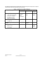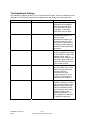
1
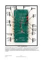
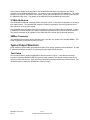
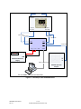
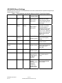
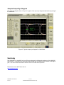
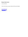
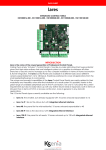
SD356EVK Evaluation Kit
Board for LMH0356 SDI
Reclocker
User Manual
National Semiconductor
EVK User Manual
Introduction
The LMH0356 Serial Digital Interface (SDI) reclocker is designed to recover a clean clock from a serial
digital video signal which may be contaminated by jitter and to resynchronize the input video data to the
recovered clean clock. The LMH0356 SDI reclocker accepts signals conforming to standards SMPTE
259M (C), SMPTE 292M, and SMPTE 424M.
The LMH0356 includes, in addition to the reclocking circuitry, an input 4-channel multiplexer which
permits selection for reclocking of any of four serial digital video signals at the inputs of the LMH0356. It
also includes fixed equalizers on its inputs designed to reduce the inter-symbol interference (ISI)
generated by dispersive PC board traces between the serial digital video source and the reclocker inputs.
The LMH0356 fixed equalizers are designed to compensate for the frequency-dependent loss of up to 30
inches of FR-4 PC board trace.
The SD356EVK is a PC board designed to aid in the evaluation of the performance characteristics of the
LMH0356 reclocker. The SD356EVK PC board is fabricated with FR-4 PC board material. The inputs
and outputs of the LMH0356 are connected to the SMA coaxial connectors on the board using controlledimpedance 50Ω single-ended and 100Ω differential PC board traces.
This instruction manual describes the features of the SD356EVK. It should be used in conjunction with
the LMH0356 SDI reclocker data sheet. Schematics and PC board layout drawings for the SD356EVK
board are included separately. In addition, board fabrication files are available on request. Contact your
local National Semiconductor representative.
PC Board Features
The SD356EVK is shown in Figure 1. The features of the board are described in the sections that follow.
General Description
The SD356EVK is a four-layer PC board fabricated using FR-4. The layer stackup is shown in drawing
number 980600057-001. As the drawing indicates, the nominal board thickness is .062 inches. The
board includes internal ground and power supply planes. The ground plane is the second layer of the
board (underneath the top layer) and is the reference for the controlled-impedance traces on the top layer.
The SD356EVK is fabricated using Pb-free solder and components and is comprised of RoHS-compliant
materials.
SDI Input and Output Connectors
The SDI input and output connectors are 50Ω SMA female coaxial connectors (jacks). These connectors
will mate non-destructively with 50Ω SMA male coaxial connectors (plugs). They will also mate nondestructively with 50Ω APC-3.5 male coaxial connectors and 2.92 mm (K) male coaxial connectors.
These connectors will NOT mate to 2.4 mm connectors. Do not attempt to connect 2.4 mm connectors to
the SD356EVK PC board. This will damage both the board and the connected device or cable.
SD356EVK User Manual
Rev 1.0
1 of 11
© 2008, National Semiconductor Corp.
SDI Input
Connectors
(50Ω SMA)
30-inch
FR4 Trace
(Input
SDI0)
Control/Indicator
LEDs
15-inch
FR4 Trace
(Input
SDI1)
DC Power
Connectors
External
Control
Header
Control
DIP
Switches
Control
Headers
SMBus
Connector
(not active)
SDI Output
Connectors
(50Ω SMA)
27 MHz
Reference
Crystal
LMH0356 SDI
Reclocker
30-inch
FR4 Trace
(Test
Coupon)
27 MHz
Reference
External
Input
Figure 1. SD356EVK board
Although the SMA coaxial connectors are ruggedized for attachment to the edge of the SD356EVK PC
board, they can be damaged by over-tightening them. A standard SMA torque wrench with a torque
limitation of 7-10 in-pounds should always be used to connect cables to the connectors on the
SD356EVK. Do not allow heavy cables to hang unsupported from the connectors as they may break off
the board.
SD356EVK User Manual
Rev 1.0
2 of 11
© 2008, National Semiconductor Corp.
The SDI input and output connectors occur in pairs as the inputs and outputs of the LMH0356 SDI
reclocker are differential. It is not necessary to terminate unused inputs. Both the inputs and outputs of
the LMH0356 SDI reclocker are internally terminated.
The SD356EVK has two sets of outputs connected to the two outputs of the LMH0356 SDI reclocker.
The first set of outputs, labeled SDO, always carry the digital video data signal unless they are muted. If
the reclocker is locked and not bypassed, these outputs carry a reclocked version of the input signal. If
the reclocker is unlocked or bypassed, these outputs carry an unmodified replica of the input signal. The
outputs may be muted by the output mute control described in a later section.
The second set of outputs of the SD356EVK, labeled SCO/SDO2, can be set either to output a copy of
the data on the first set of outputs, either reclocked or not as describe above, or to output the recovered
clock signal from the LMH0356 SDI reclocker. The clock signal is only available when the LMH0356 SDI
reclocker is locked to a valid input signal.
The inputs and outputs of the SD356EVK PC board are AC-coupled with 1 µF 0402-size coupling
capacitors. These capacitors are rated for 10 VDC working voltage. The inputs and outputs of the
SD356EVK board may be terminated in any DC voltage that does not exceed this 10 V limit relative to the
negative power supply. The coupling capacitors may be replaced with 0402-size 0Ω resistors for DCcoupled evaluation.
FR-4 Traces
Two of the inputs to the SD356EVK, inputs SDI0 and SDI1, are equipped with long FR-4 test traces. The
trace lengths are 30 inches and 15 inches respectively on the two inputs. The other two inputs are
coupled to the LMH0356 SDI reclocker through very short FR-4 traces. The FR-4 test traces are meant
to demonstrate the action of the input passive equalizers. The input passive equalizers compensate for
the ISI introduced by long PC board traces. The SD356EVK demonstrates that the performance of the
LMH0356 SDI reclocker is unaffected by up to 30 inches of lossy FR-4 trace on its inputs.
The SD356EVK also includes a 30 inch FR-4 test trace which can be used to evaluate the ISI effect
introduced by such a trace. If desired, connectors can be soldered on to this test trace and the ISI can be
measured by external test equipment. If this is desired, the same connectors used on the inputs and
outputs of the SD356EVK may be used. These connectors are specified in the bill of materials for the
SD356EVK.
DC Power Connectors
DC power is applied to the SD356EVK by means of standard .175-inch diameter binding posts. Three
power supply terminals are provided. The first is a common ground, to which the negative supply voltage
should be connected. This is the black binding post on the board. The two red binding posts on the
board are meant to provide 3.3 VDC to 1) the LMH0356 SDI reclocker alone, and 2) the remainder of the
circuitry on the SD356EVK board. The dual-supply configuration permits measurement of the current
drawn by the LMH0356 SDI reclocker independent of the other devices on the board if desired. The two
supplies may be connected together if desired using either an external jumper or the onboard header
between the 3.3 V power supply terminals.
The power supply is not regulated on the SD356EVK board so the effects of power supply variations can
be evaluated. It is recommended that the maximum supply voltage rating of the LMH0356 (4 VDC) not
be exceeded.
The LMH0356 SDI reclocker can be powered-down using its enable feature. This feature is accessible
through the control inputs described in the next section. The dual-supply configuration of the SD356EVK
can be used to observe the effect on supply current of powering down the LMH0356.
Controls and Indicators
The control lines of the LMH0356 SDI reclocker can be controlled by various means using the SD356EVK.
The primary method for controlling these lines is the DIP switches located on the SD356EVK board. The
DIP switches are labeled according to their function. When the switch actuator is pushed to the right
SD356EVK User Manual
Rev 1.0
3 of 11
© 2008, National Semiconductor Corp.
(seen from the top), the switch is closed. The schematic for the board indicates the functions of each
switch. The switch functionality is summarized in Table 1 below.
Two headers are also provided for operating the control lines of the LMH0356 SDI reclocker. The first is
located immediately below the DIP switches. This header is meant to be used with two-pin jumpers and
provides parallel functionality to the DIP switches. When a jumper is installed on the header it overrides
the function of the equivalent DIP switch.
The second header is located to the right of the DIP switches. This header is meant to provide access for
remote control of the LMH0356 SDI reclocker. When this header is used the DIP switches should all be
set in the open position and no jumpers should be installed on the control header. The connections for
this header are described in the schematic for the SD356EVK PC board. It is recommended that this
header only be used for advanced control applications and only by users familiar with the operation of the
LMH0356 SDI reclocker.
LED indicators are provided near the top of the board to indicate the state of the control inputs and the
indicator outputs of the LMH0356 SDI reclocker. The LED states and their meanings are summarized in
Table 1.
SD356EVK User Manual
Rev 1.0
4 of 11
© 2008, National Semiconductor Corp.
Function
Input Select
Rate Select
Bypass/Autobypass
Table 1. Control and Indicator Function Summary
Switch
Indicator
Switch “On”
Function and
Indication
Sel0
Sel1
Sel0
Sel1
Rate0
Rate1
Rate0
Rate1
Bypass/Autobypass
Bypass
Switch “Off”
Function and
Indication
Select line
pulled to logic 1
Select line
pulled to logic 0
Indicator light
turns red
Indicator light
turns green
Rate line pulled
to logic 1
Rate line pulled
to logic 0
Indicator light
turns red
Indicator light
turns green
LMH0356
reclocker forced
to bypass mode
LMH0356
reclocker in
normal
(autobypass)
mode
Indicator on
(red)
Indicator off
Output Mute
OP Mute
None
LMH0356
reclocker output
is muted
LMH0356
reclocker output
is active
Serial Clock Output
Enable
SCO_EN
SCO_EN
Second output
of the
SD356EVK
outputs the
recovered clock
Second output
of the
SD356EVK
outputs a copy
of the reclocked
data
Indicator on
(green)
Chip Enable
ENABLE
ENABLE
Indicator off
LMH0356 is
powered up
(active)
LMH0356 is
powered down
(inactive)
Indicator on
(green)
Indicator off
SD/HD Indication
None
SD_HD
Indicator green
indicates HD or
3 Gb/s signal or
no signal
detected
Indicator red
indicates SD
signal detected
Lock Detection
None
LOCK DET
Indicator on
(green) when
the LMH0356
reclocker is
locked to the
incoming signal
Indicator off
when the
LMH0356
reclocker is not
locked to the
incoming signal
SD356EVK User Manual
Rev 1.0
5 of 11
© 2008, National Semiconductor Corp.
There is also a header on the right side of the SD356EVK board which is connected to the SD/HD
indication of the LMH0356 SDI reclocker. It is meant to control an LMH0302 SDI cable driver. The output
polarity of the signal on this header is such that it can be connected directly to the SD/HD control input of
the LMH0302 cable driver. The header on the SD356EVK board facilitates this connection.
27 MHz Reference
The SD356EVK includes an on-board 27-MHz reference crystal. In the normal configuration of the board
this crystal is active. The LMH0356 SDI reclocker includes a crystal driver circuit that produces the 27MHz reference clock using this crystal.
The SD356EVK also includes a connector for inputting an external 27-MHz reference if desired. In order
to disable the on-board crystal a 0Ω resistor indicated on the schematic for the board must be removed.
This permits evaluation of the operation of the LMH0356 SDI reclocker with an external reference.
SMBus Connector
The LMH0356 SDI reclocker can be controlled via a 2-wire bus very similar to the standard SMBus. This
mode of operation is reserved for factory use only.
Typical Output Waveform
A test waveform can be readily generated and used to verify proper operation of the SD356EVK. In order
to generate this output waveform, the following setup procedure should be used.
Test Setup
The test setup used for testing the SD356EVK board is shown in Figure 2. Note that the test setup
includes a SyntheSys Research BERTScope as a signal generator, eye diagram measurement device,
and bit error rate test receiver. Other equivalent instruments could be used for thse measurements. The
equipment used for testing the SD356EVK is listed in Table 2.
SD356EVK User Manual
Rev 1.0
6 of 11
© 2008, National Semiconductor Corp.
UTIFlex Cable
CK+ CK-
BERTScope
Clock In
Clock Out
Data Out
Data In
Data+ Data-
Data+ Data-
UTIFlex Cable
UTIFlex Cable
UTIFlex Cable
UTIFlex Cable
SD356 EVK Board
SDI0
SDO
SDI0
SDO
SCO
UTIFlex Cable
SCO
VCC_IC VCC
3.3 V
GND
SMBus
+
GND
RF
In
HP E3610A DC Power
Supply
SMBus Controller Cable
HP8593E Spectrum
Analyzer
`
PC with SMBus Controller and Serial Port
Figure 2. Test setup for the SD356EVK board.
SD356EVK User Manual
Rev 1.0
7 of 11
© 2008, National Semiconductor Corp.
To generate the example output eye diagram shown, the PC and the spectrum analyzer are not required.
These items are used for other elements of the test procedure.
Description
Table 2. Test Equipment and Material Required
Suggested Equipment
Manufacturer
Bit Error Rate Test Set with the following:
Model
Number
BERTScope
12500B
J-Bert
N4903A
Hewlett-Packard
DC Power Supply
E3610A
Spectrum Analyzer with minimum 3 GHz
bandwidth
Hewlett-Packard
Portable Spectrum
Analyzer
8593E
Six (6) each UTIFlex coaxial cables
Micro-Coax Inc.
UTIFlex
UFB205A0-0360000000
3 Gb/s Serial Data Capability
SyntheSys
Research
Equipment Name
Agilent
Technologies
Jitter Injection Capability
Eye Diagram and Jitter
Measurement Capability
DC Power Supply
3.3 V @ 0.5 A
SMA connectors
36 inch length
SD356EVK User Manual
Rev 1.0
8 of 11
© 2008, National Semiconductor Corp.
Test Equipment Settings
The example eye diagram shown is for a 1.4835 Gb/s HD SDI signal. Similar eye diagrams can be
obtained at 2.97 Gb/s and at 270 Mb/s by changing the bit rate setting on the signal generator.
Generator Setting
Value
Comments
Data Rate
1.4835 Gb/s
Any valid SMPTE data rate
supported by the LMH0356
SDI reclocker can be used.
These rates are 270 Mb/s,
1.485 Gb/s, 1.4835 Gb/s,
2.967 Gb/s, and 2.97 Gb/s
Data Pattern
PRBS-7
This is a standard
pseudorandom pattern 127
bits long. Other
pseudorandom patterns can
be used as well as live SDI
video patterns (which are not,
in general, pseudorandom) or
the SMPTE pathological data
sequences.
Output Amplitude
200 mV
This is the specified lower limit
for the input differential voltage
for the LMH0356. Higher input
voltages can be used. A
differential input voltage of 200
mV peak-to-peak means that
each of the two inputs swings
100 mV peak-to-peak.
Output Offset
0V
The inputs of the SD356EVK
are AC coupled so the output
offset of the generator does
not matter unless it
overstresses the input
coupling capacitors. Do not
exceed 4 V output offset on
the generator to avoid this.
Injected Jitter
0 UI
If the signal generator is
capable of injecting controlled
jitter, the jitter tolerance of the
LMH0356 may be evaluated
using the SD356EVK board.
Typical settings used for jitter
tolerance testing on the
SD36EVK board are 0.7 UI
jitter amplitude at 5 MHz and
10 MHz jitter frequencies.
SD356EVK User Manual
Rev 1.0
9 of 11
© 2008, National Semiconductor Corp.
SD356EVK Board Settings
Essentially all of the settings of the SD356EVK are set to their nominal values to produce the typical eye
diagram shown in Figure 3.
Table 3. Control Settings and Indicator States to Produce Typical Eye Diagram
Function
Switch
Indicator
Switch and
Comments
Indicator State
Input Select
Sel0
Sel1
Sel0
Sel1
Both switches off
Rate0
Rate1
Rate0
Rate1
Both switches off
Bypass/Aut
obypass
Bypass
Switch off
Output Mute
OP Mute
None
Switch off
LMH0356 reclocker
output is active.
Serial Clock Output
Enable
SCO_EN
SCO_EN
Switch off
Indicator light off
This test will produce the
same results regardless
of the state of the
SCO_EN.
Chip Enable
ENABLE
Switch of
LMH0356 is powered up.
Rate Select
Bypass/Autobypass
Both indicator
lights green
Both indicator
lights green
Indicator light off
ENABLE
This is the setting for
selecting input SDI0.
Other selection settings
can be used with other
SDI inputs.
This is the setting for
automatic rate detect.
The rate selection
switches can also be set
to match the data rate
input. For a 1.4835 Gb/s
signal as described here,
Rate0 can be off and
Rate 1 on.
LMH0356 reclocker in
normal (autobypass)
mode.
Indicator light on
SD/HD Indication
None
SD_HD
Indicator green,
indicating HD or
3 Gb/s signal or
no signal
detected
The indicator will be red if
a 270 Mb/s signal is
used.
Lock Detection
None
LOCK DET
Indicator on
(green),
indicating that the
LMH0356
reclocker is
locked to the
incoming signal
The indicator will be off if
a non-supported data
rate is used.
SD356EVK User Manual
Rev 1.0
10 of 11
© 2008, National Semiconductor Corp.
Sample Output Eye Diagram
The output eye diagram shown in Figure 3 is typical of the output eye diagrams obtained during testing of
the SD356EVK.
Figure 3. Typical output eye diagram for 1.4835 Gb/s.
Summary
The SD356EVK is a simplified four-layer PC board designed to facilitate the evaluation of the LMH0356
SDI reclocker. In concept it is a simple input/output board with the LMH0356 SDI reclocker in the signal
path. This manual has described the features of the PC board and its operation.
Please also see the SDI Feature site at::
www.national.com/sdi
SD356EVK User Manual
Rev 1.0
11 of 11
© 2008, National Semiconductor Corp.
Mouser Electronics
Authorized Distributor
Click to View Pricing, Inventory, Delivery & Lifecycle Information:
Texas Instruments:
SD356EVK/NOPB