1
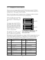
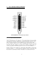
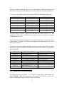
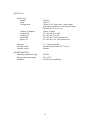
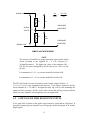
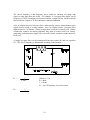
Digital I/O
CYCTM Series
Counter/Timer Boards
CYCTM 05: 5-Ch. C/T Board, 16 DIO, 100ppM, 37-pin
CYCTM 10: 10-Ch. C/T Board, 32 DIO, 100ppM, 37-pin
CYCTM 05X: High-Accuracy (50ppM) CYCTM 05, 37-pin
CYCTM 10X: High-Accuracy (50ppM) CYCTM 10, 37-pin
USER’S MANUAL
VER. 5.0
• OCT 2000
&
No part of this manual may be reproduced without permission.
CyberResearch®, Inc.
www.cyberresearch.com
25 Business Park Dr., Branford, CT 06405 USA
18
203-483-8815 (9am
to 5pm EST) FAX: 203-483-9024
This page is blank.
©Copyright 2000
All Rights Reserved.
October 2000
The information in this document is subject to change without prior notice in order
to improve reliability, design, and function and does not represent a commitment
on the part of CyberResearch, Inc.
In no event will CyberResearch, Inc. be liable for direct, indirect, special,
incidental, or consequential damages arising out of the use of or inability to use
the product or documentation, even if advised of the possibility of such damages.
This document contains proprietary information protected by copyright. All rights
are reserved. No part of this manual may be reproduced by any mechanical,
electronic, or other means in any form without prior written permission of
CyberResearch, Inc.
TRADEMARKS
“CyberResearch,” “CYCTM 05,” and “CYCTM 10” are trademarks of
CyberResearch, Inc. Other product names mentioned herein are used for
identification purposes only and may be trademarks and/or registered trademarks
of their respective companies.
• NOTICE •
CyberResearch, Inc. does not authorize any CyberResearch product for use in life
support systems, medical equipment, and/or medical devices without the written
approval of the President of CyberResearch, Inc. Life support devices and
systems are devices or systems which are intended for surgical implantation into
the body, or to support or sustain life and whose failure to perform can be
reasonably expected to result in injury. Other medical equipment includes devices
used for monitoring, data acquisition, modification, or notification purposes in
relation to life support, life sustaining, or vital statistic recording. CyberResearch
products are not designed with the components required, are not subject to
the testing required, and are not submitted to the certification required to ensure
a level of reliability appropriate for the treatment and diagnosis of humans.
i
This page is blank.
ii
TABLE OF CONTENTS
INTRODUCTION. . . . . . . . . . . . . . . . . . . . . . . . . . . . . . . . . . . . . . . . . . . . . . . . . . . i
1 SOFTWARE INSTALLATION . . . . . . . . . . . . . . . . . . . . . . . . . . . . . . . . . . . . . . 1
2 HARDWARE INSTALLATION . . . . . . . . . . . . . . . . . . . . . . . . . . . . . . . . . . . . . 2
2.1 BASE ADDRESS . . . . . . . . . . . . . . . . . . . . . . . . . . . . . . . . . . . . . . . . . . . . . . 3
2.2 INTERRUPT LEVEL SELECT . . . . . . . . . . . . . . . . . . . . . . . . . . . . . . . . . . . 4
2.3 WAIT STATE JUMPER . . . . . . . . . . . . . . . . . . . . . . . . . . . . . . . . . . . . . . . . 5
2.4 INSTALLING THE CYCTM IN THE COMPUTER . . . . . . . . . . . . . . . . . 5
3 I/O CONNECTOR & PINOUT . . . . . . . . . . . . . . . . . . . . . . . . . . . . . . . . . . . . . . . 6
3.1 CYCTM 10 SECOND 9513 . . . . . . . . . . . . . . . . . . . . . . . . . . . . . . . . . . . . . 6
4 REGISTER ARCHITECTURE . . . . . . . . . . . . . . . . . . . . . . . . . . . . . . . . . . . . . . . 7
4.1 CONTROL & DATA REGISTERS . . . . . . . . . . . . . . . . . . . . . . . . . . . . . . . . 7
4.2 CYCTM 10 & CYCTM 05 ADDRESSES . . . . . . . . . . . . . . . . . . . . . . . . . . 7
4.3 DIGITAL I/O REGISTERS . . . . . . . . . . . . . . . . . . . . . . . . . . . . . . . . . . . . . . 8
5 SPECIFICATIONS . . . . . . . . . . . . . . . . . . . . . . . . . . . . . . . . . . . . . . . . . . . . . . . . 10
6 ELECTRONICS AND INTERFACING . . . . . . . . . . . . . . . . . . . . . . . . . . . . . . 12
6.1 VOLTAGE DIVIDERS . . . . . . . . . . . . . . . . . . . . . . . . . . . . . . . . . . . . . . . . 12
6.2 LOW PASS FILTERS DE-BOUNCE INPUTS . . . . . . . . . . . . . . . . . . . . . 13
This page is blank.
INTRODUCTION
The CYCTM 10 is a single board containing two CYCTM 05 boards. From this
point forward we will refer to both boards as the CYCTM, and will only use
the complete board name in instances where items are specific to one board or the
other.
The CYCTM family is fully supported by the powerful Universal Library package.
Details regarding installation and usage of the Universal Library software can be
found in the Universal Library documentation. Please note that InstaCal (shipped with
the board) creates a configuration file required for programmers who use the
Universal Library programming libraries.
i
This page is blank.
1 SOFTWARE INSTALLATION
The CYCTM boards have a variety of switches and jumpers to set before installing
to your computer. By far the simplest way to configure a board is to use the InstaCalTM program provided as part of your software package. InstaCalTM will show you
all available options, how to configure the various switches and jumpers (as
applicable) to match your application requirements, and will create a configuration
file that your application software (and the Universal Library) will refer to so the software you use will automatically know the exact configuration of the board.
Please refer to the Extended Software Installation Manual regarding the installation
and operation of InstaCalTM. The following hard copy information is provided as a
matter of completeness, and will allow you to set the hardware configuration of the
board if you do not have immediate access to InstaCalTM and/or your computer.
1
This page is blank.
2 HARDWARE INSTALLATION
We highly recommend that you use the InstaCAL procedure to guide you through setting up your board. However, the following sections are provided in case you need to
set up your board and you do not have access to the InstaCAL program.
The CYCTM have one bank of switches, a base address switch, and one jumper block,
which must be set before installing the board in your computer.
2
2.1
BASE ADDRESS
Unless there is already a board in your
system which uses address 300h (768
Decimal) then you can leave the switches
as they are set at the factory.
In the example shown here, the CYCTM is set for base address 300h (768
Decimal).
Certain address are used by the PC, others are free and may be used by the CYCTM and other expansion boards. We recommend BASE = 300h (768D) be tried first.
HEX
RANGE
000-00F
020-021
040-043
060-063
060-064
070-071
080-08F
0A0-0A1
0A0-0AF
0C0-0DF
0F0-0FF
1F0-1FF
210-21F
238-23B
23C-23F
270-27F
2B0-2BF
FUNCTION
8237 DMA #1
8259 PIC #1
8253 TIMER
8255 PPI (XT)
8742 CONTROLLER (AT)
CMOS RAM & NMI
MASK (AT)
DMA PAGE REGISTERS
8259 PIC #2
NMI MASK (XT)
8237 #2 (AT)
80287 NUMERIC CO-P
(AT)
HARD DISK (AT)
EXPANSION UNIT (XT)
BUS MOUSE
ALT BUS MOUSE
PARALLEL PRINTER
EGA
HEX
RANGE
2C0-2CF
2D0-2DF
2E0-2E7
2E8-2EF
2F8-2FF
300-30F
FUNCTION
EGA
EGA
GPIB (AT)
SERIAL PORT
SERIAL PORT
PROTOTYPE CARD
310-31F
320-32F
378-37F
380-38F
3A0-3AF
PROTOTYPE CARD
HARD DISK (XT)
PARALLEL PRINTER
SDLC
SDLC
3B0-3BB
3C0-3CF
3D0-3DF
3E8-3EF
3F0-3F7
3F8-3FF
MDA
EGA
CGA
SERIAL PORT
FLOPPY DISK
SERIAL PORT
The CYCTM BASE switch may be set for address in the range of 000-3F8 (000-3FC
for CYCTM 05) so it should not be hard to find a free address area for your CYCTM.
Once again, if you are not using IBM prototyping cards, or some other board
that occupies these addresses, 300-31F HEX are free to use.
Address not specifically listed, such as 390-39F, are usually free.
3
2.2
INTERRUPT LEVEL SELECT
There are two rows of jumper blocks on the CYCTM 10 and one on the CYCTM 05,
located just above the PC bus interface (gold pins). The factory default setting has no
interrupt level set. The jumper is in the 'X' position.
Please leave the jumper in the 'X' position for now. Interrupts are hardware initiated
software routines and are described in the section on programming.
2
On the CYCTM 10 the lower block,
J2, is for the IR input on P1. The
upper block, J3, is for the IR input on
P2
3 4
5 6
7 X
J3
Input at P2
The trigger logic on the CYCTM is
quite simple. Pin 1 of the 37 pin connector is an input jumper which maps
the interrupt directly onto the PC bus.
The signal to the bus is buffered. The
buffer is enabled by a TTL low level
on Pin 2, interrupt enable.
J2
Input at P1
CYCTM INTERRUPT JUMPER BLOCK - IRQ
Level. The jumper is in the X position
The interrupt level jumper on the
which equals no IRQ.
CYCTM must also be installed.
Move it from the 'X' position to the
IRQ number you want the interrupt pulse on. On the CYCTM 10, jumper block J2 is associated with the signals on connector P1. Jumper block J3 is associated with the signals on connector P2. Hardware interrupts (assigned by the PC), may be available.
NAME
NMI
IRQ0
(AT)
IRQ1
IRQ2
DESCRIPTION
PARITY
TIMER
KEYBOARD
RESERVED (XT) INT
8-15 (AT)
IRQ3
COM OR SDLC
IRQ4
COM OR SDLC
IRQ5
HARD DISK (AT) LPT
(AT)
IRQ6
FLOPPY DISK
IRQ7
LPT
IRQ8-15 are AT only.
NAME
IRQ8
IRQ9
DESCRIPTION
REAL TIME CLOCK
(AT)
RE-DIRECTED TO IRQ2
IRQ10
IRQ11
UNASSIGNED
UNASSIGNED
IRQ12
IRQ13
IRQ14
UNASSIGNED
80287 NUMERIC CO-P
HARD DISK
IRQ15
UNASSIGNED
4
2.3
WAIT STATE JUMPER
ON
The CYCTM boards have a wait state
jumper which can enable an on-board
wait state generator. A wait state is an
extra delay injected into the processor's
clock via the bus. This delay slows down
the processor so that signals from slow
devices (chips) will be valid.
OFF
J1
WAIT STATE JUMPER BLOCK - For a
wait state, place the jumper on the two
leftmost pins. No wait state is selected
here.
The wait state generator on the CYCTM
is only active when the CYCTM is being
accessed. Your PC will not be slowed
down in general by using the wait state.
We recommend that the wait state be used in all 16MHz or faster PCs.
2.4
INSTALLING THE CYCTM IN THE COMPUTER
Turn the power off. Remove the cover of your computer. Please be careful not to dislodge any of the cables installed in your computer as you slide the cover off.
Locate an empty expansion slot in your computer. If you are installing a CYCTM 10,
it is best to locate two slots side by side. If you are able to free two slots next to one another,
do so.
From the rear of the computer, place the CYCTM 10 in the rightmost of the two
empty slots. This means that the empty slot is on the component side of the
CYCTM. Cabling will be easier if there is an empty slot on the component side of
the board.
Push the board firmly down into the expansion bus connector. If it is not seated fully
it may fail to work and could short circuit the PC bus power onto a PC bus signal.
This could damage the motherboard in your PC as well as the CYCTM. The CYCTM
connector is a male 37-pin D-type connector. All the signals from the 9513, digital
input, digital output and interrupt are accessible. The CYCTM 10 has two of these
connectors: P1 and P2; the signals on both are identical.
5
3
I/O CONNECTOR & PINOUT
CTR 2 IN 19
CTR 2 GATE 18
CTR 3 IN 17
CTR 3 GATE 16
CTR 4 IN 15
CTR 4 GATE 14
CTR 5 IN 13
CTR 5 GATE 12
GND 11
D OUT 0 10
D OUT 1 9
D OUT 2 8
D OUT 3 7
D OUT 4 6
D OUT 5 5
D OUT 6 4
D OUT 7 3
IR ENABLE 2
IR INPUT 1
37
36
35
34
33
32
31
30
29
28
27
26
25
24
23
22
21
20
CTR 1 GATE
CTR 1 IN
CTR 1 OUT
CTR 2 OUT
CTR 3 OUT
CTR 4 OUT
CTR 5 OUT
OSC. OUT
D IN 0
D IN 1
D IN 2
D IN 3
D IN 4
D IN 5
D IN 6
D IN 7
D IN STROBE
+5V
CYCTM CONNECTOR - View from the rear of the PC.
3.1 CYCTM 10 SECOND 9513
The CYCTM 10 has two 9513 chips on it. The second of these, the one accessible
via connector P2 at the rear of the board, is wired up identically to the 9513 on P1.
Both are Keithley/MetraByte CTM-05 compatible at the connector and the register level. Software written for the CTM-05, including Labtech Notebook, HP VEE
and other third party software can operate both 'CTM-05s'. Simply install one
CTM-05 at the BASE ADDRESS and install the other at the BASE ADDRESS + 4.
On the CYCTM 10, the second 9513 counter timer chip's address is fixed at the
board's base address + 4. If the board were configured at 300H (768 Decimal), then
the second 9513 would reside at 304h (772 Decimal). No switches need to be set.
6
4
4.1
REGISTER ARCHITECTURE
CONTROL & DATA REGISTERS
The CYCTM 10 is composed of 2 AM9513 counter timer chips. The CYCTM 05
contains one 9513. Each 9513 contains five counters of 16 bits each. Associated with
each counter are an input source, a count register, a load register, a hold register, an
output and a gate. The 9513 is extremely flexible and this flexibility can make it a
challenge to program the chip directly.
Unlike an Intel 8254 which has a single source, single gate and unique I/O address for
each counter, the 9513 is fully programmable and any counter may be internally connected to any gate and receive it's counts from a number of sources. In addition, each
counter does not have a unique I/O address. The 9513 takes only two address per
chip, one of which is a data path to the counter's load and hold registers.
There is no 9513 register information in this manual. Those wishing to know more
about the AM9513 and its programming should request the manual from our technical
support group. As of this writing there is no charge for the manual.
However, we suggest that you use the Universal Library, rather than resort to programming the 9513 directly. It is difficult to program and because programming support is available through the Universal Library, we cannot help with other 9513 programming.
4.2
CYCTM 10 & CYCTM 05 ADDRESSES
The CYCTM is an I/O mapped expansion board. The CYCTM 10 occupies eight I/O
addresses and the CYCTM 5 occupies four addresses.
The first address, or BASE ADDRESS, is determined by setting a bank of switches on
the board.
Most of the functions that this board is capable of performing can be acheived using
the Universal Library. Unless you have a good reason for direct register
manipulation, we suggest you use the Universal Library.
The register descriptions follow the format:
7
6
5
4
A7
A6
A5
A4
3
A3
7
2
A2
1
A1
0
A0
Where the numbers along the top row are the bit positions within the 8-bit byte and
the numbers and symbols in the bottom row are the functions associated with that bit.
To write to or read from a register in decimal or HEX, the following weights apply:
BIT POSITION
0
1
2
3
4
5
6
7
DECIMAL VALUE
1
2
4
8
16
32
64
128
HEX VALUE
1
2
4
8
10
20
40
80
To write control or data to a register, the individual bits must be set to 0 or 1 then
combined to form a byte. Data read from registers must be analyzed to determine
which bits are on or off.
The method of programming required to set/read bits from bytes is beyond the scope
of this manual. It will be covered in most Introduction To Programming books, available from a bookstore.
In summary form, the registers and their function are listed on the following table.
Within each register are eight bits which may constitute a byte of data or eight individual bit functions.
ADDRESS
BASE +0
BASE +1
BASE +2
BASE +3
BASE +4
BASE +5
BASE +6
BASE +7
4.3
READ FUNCTION
Data from 9513 #1
Status of 9513 #1
Digital input port, P1
No read back of output port
CYCTM 10 ONLY
Data from 9513 #2
Status of 9513 #2
Digital input port, P2
No read back of output port
WRITE FUNCTION
Data for 9513 #1
Commands to 9513 #1
Digital output port
Data for 9513 #2
Cammands to 9513 #2
Digital output port, P2
DIGITAL I/O REGISTERS
The digital input port at BASE + 2 is a 74LS373 input buffer with a strobe line.
When STROBE is high, the current status of the inputs to the 74LS373 may be read.
When STROBE goes low, the 74LS373 inputs are latched.
8
The digital output port at BASE + 3 is a 74LS273 output buffer. Each write to BASE
+ 3 places a byte of data on the output port.
9
5
SPECIFICATIONS
Typical for 25°C unless otherwise specified.
POWER CONSUMPTION
+5V
CYCTM 10
CYCTM 05
300mA typical, 500mA max
190mA typical, 320mA max
COUNTER SECTION
Counter type
Configuration
CYCTM 10
CYCTM 05
9513
Two 9513 devices. 5 counters per 9513, 16
bits each
One 9513 device. 5 counters, 16 bits each
Clock input frequency
X2 Clock input source
High pulse width (clock input)
Cycle time (clock input)
Gate pulse duration
Input low voltage
Input high voltage
Output low voltage
Output high voltage
Crystal oscillator clock source
Frequency accuracy
CYCTM 05/10
CYCTM 05X/10X
7Mhz max
1MHz (10MHz Xtal divided by 10)
70ns min
145ns min
145ns min
-0.5V min, 0.8V max
2.2V min, 5V max
0.4V max @ 3.2mA
2.4V min @ -200µA
10MHz
100pp
m
50ppm
10
DIGITAL I/O
Digital Type
Output:
Input:
Configuration
Number of channels
Output High
Output Low
Input High
Input Low
Interrupts
Interrupt enable
Interrupt sources
ENVIRONMENTAL
Operating temperature range
Storage temperature range
Humidity
74LS273
74LS373
2 banks of 8: 1 bank input, 1 bank output,
input may be latched via external strobe input
(latched on TTL low level)
8 input, 8 output
2.7 volts min @ -0.4mA
0.5 volts max @ 8 mA
2.0 volts min, 7 volts absolute max
0.8 volts max, -0.5 volts absolute min
2 - 7, jumper selectable
External, enabled with TTL low level
External
0 to 50°C
-20 to 70°C
0 to 90% non-condensing
11
6
6.1
ELECTRONICS AND INTERFACING
VOLTAGE DIVIDERS
An alternative method of measuring a signal which varies over a range greater than the
input range of a digital input, is to use a voltage divider. When correctly designed, it
can drop the voltage of the input signal to a safe level the digital input can accept.
Ohm's law states:
Voltage = Current x Resistance
Kirkoff's law states:
The sum of the voltage drops around a circuit will be equal to the voltage
drop for the entire circuit.
In a voltage divider, the voltage across one resistor in a series circuit is proportional to
the total resistance divided by the one resistor (see formula below).
The object in a voltage divider is to choose two resistors having the proportions of
the maximum voltage of the input signal to the maximum allowed input voltage.
The formula for attenuation is:
Attenuation = R1 + R2
R2
2 = 10K + 10K
10K
For example, if the signal varies between 0 and 20
volts and you wish to measure that with an analog
input with a full scale range of 0 to 10 volts, the
attenuation (A) is 2:1 or just 2.
R1 = (A-1) x R2
For a given attenuation, pick a resistor and call it
R2, the use this formula to calculate R1.
Digital inputs often require the use of voltage dividers. For example, if you wish to
measure a digital signal that is at 0 volts when off and 24 volts when on, you cannot
connect that directly to a digital input. The voltage must be dropped to 5 volts max
when on. The attenuation is 24:5 or 4.8.
Using the equation above, if R2 is 1K, R1 = (4.8−1) x 1000 = 3.8K.
Remember that a TTL input is 'on' when the input voltage is greater than 2.5 volts.
12
Vin
SIGNAL HIGH
=
R1 + R2
R2
Vout
R1
V1
A/D BOARD
SIGNAL
VOLTS Vin
HIGH INPUT
R2
V2
Vout
A/D BOARD
LOW INPUT
SIGNAL LOW
SIMPLE VOLTAGE DIVIDER
NOTE
The resistors, R1 and R2, are going to dissipate power in the divider
circuit according to the equation W = I2 x R; (Current (I) =
Voltage/Resistance). The higher the value of the resistance (R1 +
R2), the less power dissipated by the divider circuit. Here is a simple rule:
For attenuation of <5:1, no resistor should be less than 10K.
For attenuation of > 5:1, no resistor should be less than 1K.
The STA-01 has the circuitry on board to create custom voltage dividers. It
is a is a 16" by 4" screw terminal board with two 37-pin D-type connectors and 56
screw terminals (12 - 22 AWG). Designed for table top, wall, or rack mounting, the
board provides prototype, divider circuit, filter circuit and pull-up resistor positions
which you may complete with components for your application.
6.2
LOW PASS FILTERS DE-BOUNCE INPUTS
A low pass filter is placed on the signal wires between a signal and an A/D board. It
prevents frequencies greater than the cut-off frequency from entering the A/D board's
digital inputs.
13
The cut-off frequency is that frequency above which no variation of voltage with
respect to time may enter the circuit. For example, if a low-pass filter had a cut-off
frequency of 30 Hz, interference associated with line voltage (60 Hz) would be mostly
filtered out but a signal of 25 Hz would pass with less attenuation.
Also, in a digital circuit, a low-pass filter is often used to remove contact bounce noise
signals from a switch or a relay contacts. Also, in a digital circuit, a low pass filter
might be used to “de-bounce” (filter) an input from a switch or external relay. (Unless
switch/relay contacts are mercury-whetted, they tend to bounce briefly on closure,
generating a pulsating noise signal. This can easily lead to erroneous counts unless filtered out.)
A simple low-pass filter can be constructed from one resistor (R) and one capacitor
(C). The cut-off frequency is determined according to the formula:
Fc =
R=
1
2πRC
Where π= 3.14...
R = ohms
C = farads
Fc = cut-off frequency in cycles/second
1
2π C Fc
14
Notes
EC Declaration of Conformity
We, the manufacturer, declare under sole responsibility that the product:
CYCTM 05
CYCTM 10
Part Number
5 channel counter/timer board
10 channel counter/timer board
Description
to which this declaration relates, meets the essential requirements, is in conformity
with, and CE marking has been applied according to the relevant EC Directives listed
below using the relevant section of the following EC standards and other normative
documents:
EU EMC Directive 89/336/EEC: Essential requirements relating to electromagnetic
compatibility.
EU 55022 Class B: Limits and methods of measurements of radio interference
characteristics of information technology equipment.
EN 50082-1: EC generic immunity requirements.
IEC 801-2: Electrostatic discharge requirements for industrial process measurement
and control equipment.
IEC 801-3: Radiated electromagnetic field requirements for industrial process
measurements and control equipment.
IEC 801-4: Electrically fast transients for industrial process measurement and control
equipment.
15
Product Service
Diagnosis and Debug
CyberResearch, Inc. maintains technical support lines staffed by experienced
Applications Engineers and Technicians. There is no charge to call and we will
return your call promptly if it is received while our lines are busy. Most problems
encountered with data acquisition products can be solved over the phone. Signal
connections and programming are the two most common sources of difficulty.
CyberResearch support personnel can help you solve these problems, especially if
you are prepared for the call.
To ensure your call’s overall success and expediency:
1) Have the phone close to the PC so you can conveniently and quickly take action
that the Applications Engineer might suggest.
2) Be prepared to open your PC, remove boards, report back-switch or jumper
settings, and possibly change settings before reinstalling the modules.
3) Have a volt meter handy to take measurements of the signals you are trying to
measure as well as the signals on the board, module, or power supply.
4) Isolate problem areas that are not working as you expected.
5) Have the source code to the program you are having trouble with available so
that preceding and prerequisite modes can be referenced and discussed.
6) Have the manual at hand. Also have the product’s utility disks and any other
relevant disks nearby so programs and version numbers can be checked.
Preparation will facilitate the diagnosis procedure, save you time, and avoid repeated
calls. Here are a few preliminary actions you can take before you call which may
solve some of the more common problems:
1) Check the PC-bus power and any power supply signals.
2) Check the voltage level of the signal between SIGNAL HIGH and SIGNAL LOW,
or SIGNAL+ and SIGNAL– . It CANNOT exceed the full scale range of the board.
3) Check the other boards in your PC or modules on the network for address and
interrupt conflicts.
4) Refer to the example programs as a baseline for comparing code.
16
Warranty Notice
CyberResearch, Inc. warrants that this equipment as furnished will be free from
defects in material and workmanship for a period of one year from the confirmed
date of purchase by the original buyer and that upon written notice of any such
defect, CyberResearch, Inc. will, at its option, repair or replace the defective item
under the terms of this warranty, subject to the provisions and specific exclusions
listed herein.
This warranty shall not apply to equipment that has been previously repaired or
altered outside our plant in any way which may, in the judgment of the manufacturer,
affect its reliability. Nor will it apply if the equipment has been used in a manner
exceeding or inconsistent with its specifications or if the serial number has been
removed.
CyberResearch, Inc. does not assume any liability for consequential damages
as a result from our products uses, and in any event our liability shall not exceed
the original selling price of the equipment.
The equipment warranty shall constitute the sole and exclusive remedy of any Buyer
of Seller equipment and the sole and exclusive liability of the Seller, its successors
or assigns, in connection with equipment purchased and in lieu of all other warranties expressed implied or statutory, including, but not limited to, any implied
warranty of merchant ability or fitness and all other obligations or liabilities of seller,
its successors or assigns.
The equipment must be returned postage prepaid. Package it securely and insure it.
You will be charged for parts and labor if the warranty period has expired.
Returns and RMAs
If a CyberResearch product has been diagnosed as being non-functional, is visibly
damaged, or must be returned for any other reason, please call for an assigned
RMA number. The RMA number is a key piece of information that lets us track and
process returned merchandise with the fastest possible turnaround time.
PLEASE CALL FOR AN RMA NUMBER!
Packages returned without an RMA number will be refused!
In most cases, a returned package will be refused at the receiving dock if its
contents are not known. The RMA number allows us to reference the history of
returned products and determine if they are meeting your application’s requirements. When you call customer service for your RMA number, you will be asked to
provide information about the product you are returning, your address, and
a contact person at your organization.
17
For your notes.