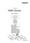
1
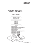
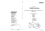
V680-series ID Flag Sensors
User’s Manual
ID Flag Sensors
V680-HAM91
V680-HAM81
Antennas
V680-HS51
V680-HS52
V680-HS63
V680-HS65
RF Tags
V680-D1KP52MT
V680-D1KP53M
V680-D1KP52M-BT01/D1KP52M-BT11
V680-D1KP66T/-D1KP66MT
V680-D1KP66T-SP
V680-D1KP58HTN
V680-D2KF52M
V680-D2KF52M-BT01/D2KF52M-BT11
V680-D8KF67/-D8KF67M
V680-D8KF68/-D32KF68
V680S-D2KF67/-D2KF67M
V680S-D2KF68/-D2KF68M
V680S-D8KF67/-D8KF67M
V680S-D8KF68/-D8KF68M
Man. No.: Z279-E1-06
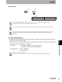
Introduction
Thank you for purchasing a V680/V680S-series ID System. This manual describes the functions,
performance, and application methods needed for optimum use of the V680-series RFID System.
Please observe the following items when using the ID System.
• Allow the ID System to be installed and operated only by qualified specialist with a sufficient knowledge of
electrical systems.
• Read and understand this manual before attempting to use the ID System and use the ID System correctly.
• Keep this manual in a safe and accessible location so that it is available for reference when required.
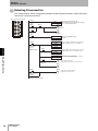
Section 1 Section 2 Section 3 Section 4 Section 5 Section 6 Section 7
Section 1 Product Overview
Section 2 Names and Functions of Components
Section 3 Functions
Section 4 Installation, Connections, and Wiring
Section 5 Control I/O Interface
Section 6 Troubleshooting
Section 7 Appendices
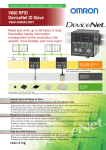
RFID System
V680-HAM91
V680-HAM81
V680-HS51
V680-HS52
V680-HS63
V680-HS65
V680-1KP52MT
V680-1KP52MT-BT01/-D1KP52M-BT11
V680-1KP53M
V680-1KP66T/-D1KP66MT
V680-1KP66T-SP
V680-1KP58HTN
V680-2KF52M
V680-2KF52MT-BT01/-D2KF52M-BT11
V680-8KF67/-D8KF67M
V680-D8KF68/-D32KF68
V680S-2KF67/-D2KF67M
V680S-2KF68/-D2KF68M
V680S-8KF67/-D8KF67M
V680S-8KF68/-D8KF68M
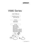
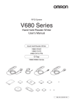
User's Manual
Introduction
Introduc- READ AND UNDERSTAND THIS DOCUMENT
tion
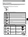
ID Flag Sensor
ID Flag Sensor
Antenna
Antenna
Antenna
Antenna
RF Tag
RF Tag
RF Tag
RF Tag
RF Tag
RF Tag
RF Tag
RF Tag
RF Tag
RF Tag
RF Tag
RF Tag
RF Tag
RF Tag
Introduction
Introduction
READ AND UNDERSTAND THIS DOCUMENT
Please read and understand this document before using the products. Please consult your OMRON representative if you have any questions or comments.
WARRANTY
OMRON’s exclusive warranty is that the products are free from defects in materials and workmanship for a period of one year (or other period if specified)
from date of sale by OMRON.
OMRON MAKES NO WARRANTY OR REPRESENTATION, EXPRESS OR IMPLIED, REGARDING NON-INFRINGEMENT, MERCHANTABILITY, OR FITNESS FOR PARTICULAR PURPOSE OF THE PRODUCTS. ANY BUYER OR USER ACKNOWLEDGES THAT THE BUYER OR USER ALONE HAS
DETERMINED THAT THE PRODUCTS WILL SUITABLY MEET THE REQUIREMENTS OF THEIR INTENDED USE. OMRON DISCLAIMS ALL OTHER
WARRANTIES, EXPRESS OR IMPLIED.
LIMITATIONS OF LIABILITY
OMRON SHALL NOT BE RESPONSIBLE FOR SPECIAL, INDIRECT, OR CONSEQUENTIAL DAMAGES, LOSS OF PROFITS OR COMMERCIAL LOSS IN
ANY WAY CONNECTED WITH THE PRODUCTS, WHETHER SUCH CLAIM IS BASED ON CONTRACT, WARRANTY, NEGLIGENCE, OR STRICT LIABILITY.
In no event shall responsibility of OMRON for any act exceed the individual price of the product on which liability is asserted.
IN NO EVENT SHALL OMRON BE RESPONSIBLE FOR WARRANTY, REPAIR, OR OTHER CLAIMS REGARDING THE PRODUCTS UNLESS OMRON’S
ANALYSIS CONFIRMS THAT THE PRODUCTS WERE PROPERLY HANDLED, STORED, INSTALLED, AND MAINTAINED AND NOT SUBJECT TO CONTAMINATION, ABUSE, MISUSE, OR INAPPROPRIATE MODIFICATION OR REPAIR.
SUITABILITY FOR USE
THE PRODUCTS CONTAINED IN THIS DOCUMENT ARE NOT SAFETY RATED. THEY ARE NOT DESIGNED OR RATED FOR ENSURING SAFETY OF
PERSONS, AND SHOULD NOT BE RELIED UPON AS A SAFETY COMPONENT OR PROTECTIVE DEVICE FOR SUCH PURPOSES. Please refer to separate catalogs for OMRON's safety rated products.
OMRON shall not be responsible for conformity with any standards, codes, or regulations that apply to the combination of products in the customer’s application or use of the product.
At the customer’s request, OMRON will provide applicable third party certification documents identifying ratings and limitations of use that apply to the products. This information by itself is not sufficient for a complete determination of the suitability of the products in combination with the end product, machine,
system, or other application or use.
The following are some examples of applications for which particular attention must be given. This is not intended to be an exhaustive list of all possible uses
of the products, nor is it intended to imply that the uses listed may be suitable for the products:
• Outdoor use, uses involving potential chemical contamination or electrical interference, or conditions or uses not described in this document.
• Nuclear energy control systems, combustion systems, railroad systems, aviation systems, medical equipment, amusement machines, vehicles, safety
equipment, and installations subject to separate industry or government regulations.
• Systems, machines, and equipment that could present a risk to life or property.
Please know and observe all prohibitions of use applicable to the products.
NEVER USE THE PRODUCTS FOR AN APPLICATION INVOLVING SERIOUS RISK TO LIFE OR PROPERTY WITHOUT ENSURING THAT THE SYSTEM
AS A WHOLE HAS BEEN DESIGNED TO ADDRESS THE RISKS, AND THAT THE OMRON PRODUCT IS PROPERLY RATED AND INSTALLED FOR THE
INTENDED USE WITHIN THE OVERALL EQUIPMENT OR SYSTEM.
PERFORMANCE DATA
Performance data given in this document is provided as a guide for the user in determining suitability and does not constitute a warranty. It may represent the
result of OMRON’s test conditions, and the users must correlate it to actual application requirements. Actual performance is subject to the OMRON Warranty
and Limitations of Liability.
CHANGE IN SPECIFICATIONS
Product specifications and accessories may be changed at any time based on improvements and other reasons.
It is our practice to change model numbers when published ratings or features are changed, or when significant construction changes are made. However,
some specifications of the product may be changed without any notice. When in doubt, special model numbers may be assigned to fix or establish key specifications for your application on your request. Please consult with your OMRON representative at any time to confirm actual specifications of purchased products.
DIMENSIONS AND WEIGHTS
Dimensions and weights are nominal and are not to be used for manufacturing purposes, even when tolerances are shown.
ERRORS AND OMISSIONS
The information in this document has been carefully checked and is believed to be accurate; however, no responsibility is assumed for clerical, typographical,
or proofreading errors, or omissions.
PROGRAMMABLE PRODUCTS
OMRON shall not be responsible for the user’s programming of a programmable product, or any consequence thereof.
COPYRIGHT AND COPY PERMISSION
This document shall not be copied for sales or promotions without permission. This document is protected by copyright and is intended solely for use in conjunction with the product. Please notify us before copying or reproducing this document in any manner, for any other purpose. If copying or transmitting this
document to another, please copy or transmit it in its entirety.
2
RFID System
User's Manual
Introduction
Introduction
Safety Precautions
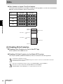
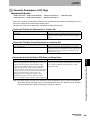
Alert Symbols for Safe Use
The following symbols are used in this manual to indicate precautions that must be observed to ensure safe
use of V680-HAM91, V680-HAM81, V680-series Antennas, and V680/V680S-series RF Tags.
The precautions provided here contain important safety information. Be sure to observe these precautions.
The following signal words are used in this manual.
WARNING
Indicates a potentially hazardous situation which, if not avoided, will result in minor or moderate injury, or may result in serious injury or death. Additionally, there may be significant
property damage.
Meanings of Alert Symbols
Indicates general prohibitions for which there is no specific symbol.
Warning
WARNING
These Products are not designed to be used either directly or indirectly in applications that detect human
presence for the purpose of maintaining safety. Do not use these Products as a sensing means for protecting
human lives.
RFID System
User's Manual
3
Introduction
Introduction
Precautions for Safe Use
Be sure to observe the following precautions to ensure safe use of the Products.
1. Do not use the Products in environments with flammable, explosive, or corrosive gasses.
2. Do not attempt to disassemble, repair, or modify any Product.
3. Because a cable has a locking mechanism, make sure that it has been locked before using the cable.
4. Make sure the power supplied by the DC power supply unit is within the rated power supply voltage (24
VDC +10%/15%) before using the Product.
5. Do not connect the power supply in reverse.
6. Do not allow water or pieces of wire to enter from openings in the case. Doing so may cause fire or electric
shock.
7. Provide sufficient ventilation space.
8. Do not install the Products near any equipment that generates a large amount of heat (such as heaters,
transformers, and large-capacity resistors).
9. Turn OFF the Controller power supply before mounting or removing an Antenna.
10. If an error is detected in any Product, immediately stop operation and turn OFF the power supply. Consult
with an OMRON representative.
11. Dispose of the Products as industrial waste.
12. Using thinner, benzene, acetone, or kerosene for cleaning may affect the resin parts and the surface of the
case. For detail, refer Chemical Resistance of the Antennas and RF Tags on page 202 and do not use
chemicals that affect the resin parts and the surface of the case.
13. If multiple Antennas are mounted near each other, communications performance may decrease due to
mutual interference. Refer to Mutual Interference between Antennas (Reference) on page 149 and check
to make sure there is no mutual interference between the Antennas.
14. To remove the Unit, catch a tool on the hook and gently remove the Unit.
15. Do not perform wiring incorrectly or short-circuit the load. Doing so may result in rupture or damage from
burning.
16. Do not use the product in environments subject to oil.
17. Do not never use the AC power supply.
4
RFID System
User's Manual
Introduction
Introduction
Precautions for Correct Use
Always observe the following precautions to prevent operation failures, malfunctions, and adverse effects on
performance and equipment.
1. Installation and Storage Environment
Do not use or store the Product in the following locations.
•Locations subject to corrosive gases, dust, dirt, metal powder, or salt.
•Locations where the specified ambient temperature and ambient humidity range is exceeded.
•Locations subject to extreme temperature changes that may result in condensation.
•Locations where the product would be directly subjected to vibration or shock exceeding specifications.
•Locations subject to contact with water, oil, or chemicals
2. Installation
•The Products communicate with RF Tags using the 13.56-MHz frequency band. Some motors,
inverters, and switching power supplies generate noise that can affect communications with the RF
Tags and cause errors. If such devices are located near the RF Tags, always test operation in advance
to confirm whether the system will be affected.
•Observe the following precautions to minimize the effects of normal noise.
(1) Ground all metal objects in the vicinity of the Products to 100 or less.
(2) Do not use the Products near high-voltage or high-current lines.
•Do not pull on the cables with excessive strength.
•The Product is not waterproof. Do not use it in an environment where mist is present.
•Do not expose the Products to chemicals that adversely affect the Product materials.
•The dust cover is attached at the CN2 connector. When neither writing in the RF Tags nor address
shift function/noise check function is used, the connection to this connector is unnecessary. In this
case, please keep the duct cover attached.
•The communications range is adversely affected if there is any metal material around the RF Tag.
•Transmission will not be possible if the front and back panels are mistakenly reversed and the Unit is
mounted to a metallic surface.
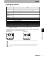
V680-D1KP66MT
V680S-D2KF67M
V680S-D2KF68M
V680S-D8KF67M
V680S-D8KF68M
•The transmission distance will be reduced when the Unit is not mounted to a metallic surface.
mounted to a metallic surface.
V680-D1KP66MT
V680S-D2KF67M
V680S-D2KF68M
V680S-D8KF67M
V680S-D8KF68M
•The maximum communications range can be obtained when the Antenna faces the RF tag directly.
When the RF tag is installed at a tilt, the communications range is reduced. Consider the effect of the
RF tag at tilt when installing the RF Tag.
RFID System
User's Manual
5
Introduction
Introduction
•Provide the mounting distances between plural RF tags to prevent them from malfunctions due to
mutual interference.
•If the central axis of an antenna and RF tag shifts, a communications range will fall.
•Do not touch the product immediately after usage at high temperatures. Doing so may occasionally
result in burning.
3. About control at the initial state
There is a possibility that the state of Input/Output becomes unstable while starting this product.
Please control Input/Output after one second or more passes after turning on the power supply to this
product.
4. Use at high temperatures (V680-D1KP58HTN)
• Data stored in memory in the RF Tag may be lost due to the characteristics of EEPROM, if the accumulated usage time of the RF Tag at a high temperature over 125C exceeds 10 hours after writing
data to the RF Tag.
• Do not communicate between the Antenna and the RF Tag in an environment where the ambient
operating temperature is 85C or higher.
An error in communications between the Antenna and the RF Tag may occur.
• Do not use the commands using UID (unique identification number for each RF Tag) when the RF tag
is used at a high temperature over 125C. The UID may be lost due to the characteristics of
EEPROM.
For Use at high temperatures, refer to Product Specifications - Use at high temperatures (V680-D1KP58HTN) in Section 7 Appendices.
p.97
6
RFID System
User's Manual
Introduction
Introduction Meanings of Symbols
Meanings of Symbols
Indicates particularly important points related to a function, including precautions and application advice.
Indicates page numbers containing relevant information.
Indicates reference to helpful information and explanations for difficult terminology.
RFID System
User's Manual
7
Introduction
Introduction Meanings of Symbols
8
MEMO
RFID System
User's Manual
Introduction
Introcuction
Table of Contents
Introduction
Safety Precautions
3
Precautions for Safe Use
4
Precautions for Correct Use
5
Meanings of Symbols
7
Table of Contents
9
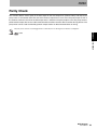
Section 1 Product Overview
11
Features
12
System Configuration
13
Section 2 Names and Functions of Components
15
ID Flag Sensor
16
Antennas
23
RF Tags
24
Section 3 Functions
27
Communications Mode
28
Optional Functions
30
Wire-saving Mode
32
Parity Check
33
Address Shift
34
Noise Measurement
35
Write Protection
36
Section 4 Installation, Connections, and Wiring
39
ID Flag Sensor
40
Installing Antennas
45
Installing RF Tags
48
RFID System
User's Manual
9
Introduction
Introduction
Section 5 Control I/O Interface
I/O Interface Control
58
I/O Control Flow
59
Timing Charts
60
Sample Programming
69
Section 6 Troubleshooting
73
Handling Errors
74
Errors and Countermeasures
75
Maintenance and Inspection
76
Section 7 Appendices
Product Specifications
77
78
Characteristics
110
Reference Data: Antenna and RF Tags Installation
151
RF Tag Memory Capacities and Memory Types
199
RF Tag Memory Map
200
Chemical Resistance of the Antennas and RF Tags
202
V600-Compatible Mode
208
Degree of Protection
223
Revision History
10
57
RFID System
User's Manual
226
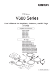
Section 1
Section 1
Product Overview
12
System Configuration
13
RFID System
User’s Manual
Product Overview
Features
11
Section 1
Product Overview
Features
The V680-series ID System uses electromagnetic induction in the 13.56-MHz bandwidth, which conforms to
Section 1 Features
the international standards in ISO/IEC 18000-3 (ISO/IEC 15693). A V680-series ID System enables reading
and writing RF Tag data without contact by connecting a V680-HAM91/V680-HAM81 ID Flag Sensor to a
V680-series Antenna. With control performed in connection with the Basic I/O Units of a Programmable
Controller, ID Flag Sensors provide data management for applications such as quality and process control at
production sites.
Simple Operation with I/O Control as Simple as Using a Regular Sensor
The V680-HAM91 and V680-HAM81 can be used right away to create an RFID System with operation
as easy as with regular Sensors. Start operation simply by setting the mode switch on the ID Flag
Sensor to output the read results to the I/O interface.
Advanced Line Management
In accessing RF Tag data, up to 64,000 IDs are possible with 16-bit data. And, using the address shift
function enables accessing up to 128 bits, making it possible to build advanced lines.
Conforms to International Standards of ISO/IEC 18000-3 (ISO/IEC 15693)
Compliance with international standards enables the V680 to be exported to and used in the world's
main countries.
RF Tags Available with EEPROM or FRAM
Two types of RF Tag memory are available: EEPROM, with a maximum heat resistance of 180C
(30 min./200 cycles) and a capacity of 1,000 bytes, and FRAM, with a capacity of 2, 8, or 32 kilobytes,
and long memory life of 10 billion accesses. Chose the ideal type for various worksite applications.
Smooth Replacement of Previous RFID Systems
All functions of the previous V600 Series are supported, so assets on existing lines can still be used.
12
RFID System
User's Manual
Section 1
Product Overview
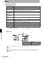
System Configuration
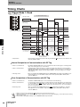
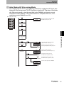
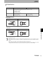
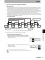
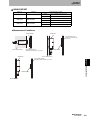
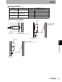
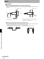
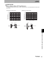
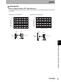
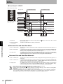
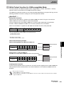
The ID Flag Sensor is connected to a Programmable Controller or wire-reduction device using I/O Interface.
Section 1 System Configuration
The ID Flag Sensor can be connected with a connector by using a optional interface cable. All of the various
V680-series Antennas and RF Tags can be used.
Host
Programmable Controllers,
Link Terminal (B7A),
I/O Relay Terminal etc.
Sensor Controller
Terminal block wiring
Interface Cable
V680-A60 2 m
5m
10 m
Connector connection
ID Flag Sensor
V680-HAM81
V680-HAM91
Connector connection
Antenna
V680-HS51
V680-HS65-R
V680-HS65-W
V680-HS63-R
V680-HS63-W
V680-HS52-R
V680-HS52-W
Wireless Communications
RF Tags
V680-D1KP52MT
V680-D2KF52M
V680-D1KP52M-BT01
V680-D1KP52M-BT11
V680-D2KF52M-BT01
V680-D2KF52M-BT11
V680-D1KP53M
V680-D1KP66T
V680-D1KP66MT
V680-D1KP66T-SP
V680-D8KF67
V680-D8KF67M
V680S-D2KF67
V680S-D2KF67M
V680S-D8KF67
V680S-D8KF67M
V680-D8KF68
V680-D32KF68
V680S-D2KF68
V680S-D2KF68M
V680S-D8KF68
V680S-D8KF68M
V680-D1KP58HTN
When embedding the V680-D1KP52MT, V680-D1KP53M, and V680-D2KF52M in a metal surface, please use the
V680-HS51 or -HS52 Antenna. It can not communicate with the V680-HS63 Antenna.
When using a V680S-D8KF@@ , to use the ID Flag Sensor production after October 2014.
RFID System
User's Manual
13
Section 1
Product Overview
MEMO
Section 1 System Configuration
14
RFID System
User's Manual
Section 2
Names and Functions of Components
Section 2
16
Antennas
23
RF Tags
24
RFID System
User's Manual
Names and Functions of Components
ID Flag Sensor
15
Section 2
Names and Functions of Components
ID Flag Sensor
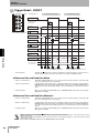
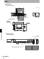
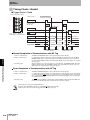
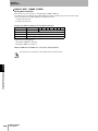
Interface Connector : CN1
Connect to 24VDC power, INHIBIT/TRIG Input and Outputs.
Recommended Power Supply : S8VS-03024(OMRON)
Note. Please use the Interface Cable(Optional).
Section 2 ID Flag Sensor
Interface Connector : CN2
Connect to Inputs.
Note. Please use the optional Interface Cable(Optional).
State Indicator LED
RUN : ID Flag Sensor Status(Green)
T/R : RF Tag communications status(Yellow)
NORMAL/ERROR : IF Flag Sensor operation result(Green/Red)
READ/WRITE : READ or WRITE operation status(Green/Yellow)
VERIFY OK/NG : Verify Read operation result(Green/Red)
Data Display LED
Date Display(Green)
Error Code Display(Red)
Noise Level Display (Green)
Mode Switches
IF Flag Sensor Operation Mode setting switches.
Access Mode Setting Switch : Set the access mode to the RF Tags.
Output Mode Setting Switch : Set the output mode and output time.
Read Mode Setting Switch : Set the read operation mode.
Write Mode Setting Switch : Set the write operation mode.
Access Address Setting
Set the access address to the RF Tag in hexadecimal notation (0000 hex to
FFFF hex)
Antenna Connector
Connects to V680-series Antennas.
16
RFID System
User's Manual
Section 2
Names and Functions of Components
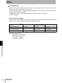
Status Indicator LED
RUN
The ID Flag Sensor status is displayed.
Status
Definition
Lit green
Normal
Not lit
No power supply or Fatal error.
Section 2 ID Flag Sensor
T/R
The communication status with the RF Tags is displayed.
Status
Definition
Lit yellow
Communicating with RF Tag , Measuring Noise level.
Not lit
Standby
NORMAL ERROR
The ID Flag Sensor operation result is displayed.
Status
Definition
Lit green
Normal Completion
Lit red
Error occurred
Not lit
Standby
READ/WRITE
The Read or Write operation mode is displayed.
Status
Definition
Lit green
Read operation
Lit yellow
Write operation
Not lit
Standby or Noise check operation
VERIFY OK/NG
The Verify Read operation result is displayed.
Status
Definition
Lit green
Verification result is matched.
Lit red
Verification result is mismatched.
Not lit
Standby
Data Display LED
The Data Display LED show the 16 bits of data that was read or
written when communication complete normally, and show the
Error Code when error was occurred. It also show the Noise Level
when measured the noise level.
Status
Definition
Lit green
Data ( Read, Write, Noise Level )
Flashing
red/Lit red
Error Code
Not lit
Standby
RFID System
User's Manual
17
Section 2
Names and Functions of Components
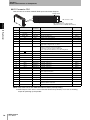
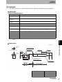
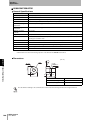
I/O Connector CN1
CN1 connects to 24 VDC, INHIBIT/TRIG input and all other Outputs.
Triangle mark
25
1
26
2
I/O connector : CN1
Section 2 ID Flag Sensor
ID Flag Sensor connectors viewed from mating side
MIL-compliant Connector (MIL-C-83503)
(Applicable Connector: OMRON XG4A-2639-A)
Name
Wire colors
(See Note1.)
1
FG
FG line
2
Not used.
---
Pin
3
Not used.
---
4
NOISE_OUT
Gray/Red
Description
I/O
FG ground terminal
FG
---
---
--ON when checking noise
--Output
5
0V
Blue
24-VDC power supply GND line
Power supply
6
24 VDC
Brown
24-VDC power supply input line
Power supply
7
PARITY
Gray/White
Parity check output (Even: OFF, Odd: ON)
Output
8
INHIBIT/TRIG
Red
Inhibit input for auto modes 1, 2, and 3
Trigger input for trigger modes 1, 2, and 3
Input
9
NORMAL/STRB
Light green
10
ERR
Purple
11
OD9
White/Red
Read data output bit 10
Output
12
OD8
White/Black
Read data output bit 9
Output
13
OD11
White/Yellow
Read data output bit 12
Outpu
14
OD10
White/Green
Read data output bit 11
Output
15
OD13
White/Blue
Read data output bit 14
Output
16
OD12
White/Brown
Read data output bit 13
Output
17
OD15
Gray/Black
Read data output bit 16
Output
18
OD14
White/Orange
Read data output bit 15
Output
19
OD1
Yellow
Read data output bit 2
Output
20
OD0
Green
Read data output bit 1
Match output in Verify Mode
Output
21
OD3
Black
Read data output bit 4
Output
Normal read completion output in Read Mode
Output for verification results in Verify Mode
Normal write completion output for Write Mode
Strobe output when Read Mode is set to Wire-saving Mode
Output
Error output (OFF: active) (See Note2.)
Output
22
OD2
White
Read data output bit 3
Output
23
OD5
Orange
Read data output bit 6
Output
24
OD4
Gray
Read data output bit 5
Output
25
OD7
Pink
Read data output bit 8
Mismatch output in Verify Mode
Output
26
OD6
Light blue
Read data output bit 7
Output
Note1: Wire colors are for the V680-A60 Interface Cable (sold separately).
2: ERR Output is OFF active. It turns ON after Powered-up correctly. It can use as checking
output for powering up the product.
18
RFID System
User's Manual
Section 2
Names and Functions of Components
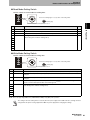
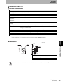
I/O Connector CN2
CN2 connects to Input signals except for INHIBIT/TRIG.
Triangle mark
25
1
26
2
I/O connector : CN2
Section 2 ID Flag Sensor
ID Flag Sensor connectors viewed from mating side
MIL-compliant Connector (MIL-C-83503)
(Applicable Connector: OMRON XG4A-2639-A)
Name
Wire colors
(See Note.)
1
FG
FG line
FG ground terminal
FG
2
Not used.
---
---
---
3
Not used
---
---
---
4
Not used
Gray/Red
5
R/W
Blue
6
NOISE_IN/WRITE
PROTECT
Brown
7
ADR2
Gray/White
8
Not used
Red
Pin No..
Description
I/O
---
---
Read/write mode switching input (Read: OFF, Write: ON)
Input
Noise check mode setting input (Noise check : ON in Read mode)
Write protect enable/disable input (Enabled : OFF, Disabled : ON in Write mode)
Input
Address shift input bit 2
Input
---
Input
9
ADR0
Light green
Address shift input bit 0
Input
10
ADR1
Purple
Address shift input bit 1
Input
11
ID9
White/Red
Write data input bit 10 in Write Mode.
Verify data input bit 10 in Verify Mode
Input
12
ID8
White/Black
Write data input bit 9 in Write Mode
Verify data input bit 9 in Verify Mode
Input
13
ID11
White/Yellow
Write data input bit 12 in Write Mode
Verify data input bit 12 in Verify Mode
Input
14
ID10
White/Green
Write data input bit 11 in Write Mode
Verify data input bit 11 in Verify Mode
Input
15
ID13
White/Blue
Write data input bit 14 in Write Mode
Verify data input bit 14 in Verify Mode
Input
16
ID12
White/Brown
Write data input bit 13 in Write Mode
Verify data input bit 13 in Verify Mode
Input
17
ID15
Gray/Black
Write data input bit 16 in Write Mode
Verify data input bit 16 in Verify Mode
Input
18
ID14
White/Orange
Write data input bit 15 in Write Mode
Verify data input bit 15 in Verify Mode
Input
19
ID1
Yellow
Write data input bit 2 in Write Mode
Verify data input bit 2 in Verify Mode
Input
20
ID0
Green
Write data input bit 1 in Write Mode
Verify data input bit 1 in Verify Mode
Input
21
ID3
Black
Write data input bit 4 in Write Mode
Verify data input bit 4 in Verify Mode
Input
22
ID2
White
Write data input bit 3 in Write Mode
Verify data input bit 3 in Verify Mode
Input
23
ID5
Orange
Write data input bit 6 in Write Mode
Verify data input bit 6 in Verify Mode
Input
24
ID4
Gray
Write data input bit 5 in Write Mode
Verify data input bit 5 in Verify Mode
Input
25
ID7
Pink
Write data input bit 8 in Write Mode
Verify data input bit 8 in Verify Mode
Input
26
ID6
Light blue
Write data input bit 7 in Write Mode
Verify data input bit 7 in Verify Mode
Input
Note: Wire colors are for the V680-A60 Interface Cable (sold separately).
This connector is not required if data will not be written to RF Tags or the address shift function and noise check function
will not be used.
RFID System
User's Manual
19
Section 2
Names and Functions of Components
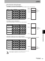
Mode Setting Switches
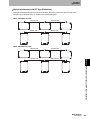
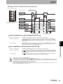
Access Mode Setting Switch
Use this switch to set the communications mode for communications with RF Tags.
Refer to the following figure for a set position of the Setting Switch.
Section 2 ID Flag Sensor
Cutting edge
Example) When it sets "1".
No.
Name
Remarks
0
SYNC1
TRIGGER MODE 1 : The ID Flag Sensor starts to communicate with RF Tags when the trigger signal inputs.
1
AUTO1
AUTO MODE 1 : The ID Flag Sensor starts to communicate with RF Tags automatically when the RF Tag comes p.64
in the communication area.
2
SYNC2
TRIGGER MODE 2 : Functional compatible mode with V600 series (V600-HAM91/-HAM81/-HAR91/-HAR81)
p.210
3
AUTO2
AUTO MODE 2 : Functional compatible mode with V600 series (V600-HAM91/-HAM81/-HAR91/-HAR81)
p.213
4
SYNC3
TRIGGER MODE 3 : Functional compatible mode of V600 series (V600-HAR92)
p.216
5
AUTO3
AUTO MODE 3 : Functional compatible mode of V600 series (V600-HAR92)
p.218
6
NOISE
CHECK
NOISE MEASURING MODE : The maintenance mode to measure the environmental noise level.
p.67
7
---
p.60
Setting Prohibit
(The ID Flag Sensor indicates Settings Error.)
8
9
Output Mode Setting Switch
Use this switch to set the output mode and output time width.
Refer to the following figure for a set position of the Setting Switch.
Cutting edge
Example) When it sets "1".
No.
Setting
Setting
Combination with the access mode
0
10 ms OFF DELAY
10 ms OFF delay
1
50 ms OFF DELAY
50 ms OFF delay
2
500 ms OFF DELAY
500 ms OFF delay
3
10 ms
10 ms output
4
50 ms
50 ms output
5
CONTINUOUS
Continuous output
6
---
Setting prohibited : except for Trigger Mode1(See Note.)
(The ID Flag Sensor indicates Settings Error.)
7
Auto Mode 1, Auto Mode 3, or Trigger Mode 3
Note: A mode setting error will occur if one of the above
access modes is not set.
Auto Mode 2 or Trigger Mode 3
Note: A mode setting error will occur if one of the above
access modes is not set.
8
9
Note. TRIGGER MODE 1 is not influenced the OUTPUT MODE settings. Set the OUTPUT mode switch either from "0" to "9".
The setting of the mode setting switch is read only when the power supply is turned ON. Therefore, settings cannot be
changed while the power is being supplied. Turn OFF the power supply before changing the settings.
20
RFID System
User's Manual
Section 2
Names and Functions of Components
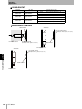
Read Mode Setting Switch
Use this switch to set the mode for reading data.
Refer to the following figure for a set position of the Setting Switch.
Cutting edge
Section 2 ID Flag Sensor
Example) When it sets "1".
No
.
Name
0
DATA READ1
Outputs read data.
1
DATA READ2
Outputs read data in Wire-saving Mode.
p.32
2
VERIFY
Compares external input data with read data and outputs the verification result.
p.31
3
---
Setting prohibited.
(The ID Flag Sensor indicates Settings Error.)
---
4
Description
5
6
7
8
9
Write Mode Setting Switch
Use this switch to set the mode for writing data.
Refer to the following figure for a set position of the Setting Switch.
Cutting edge
Example) When it sets "1".
No.
Name
0
2-BYTE WRITE
Write the 2 bytes (16 bits) of data that is input to the external data inputs (ID 0 to ID15) to the RF Tag.
1
BIT SET
When external data (ID0 to ID15) is input, only the ON bits will be turned ON. The other bits will not be
changed.
2
BIT CLEAR
When external data (ID0 to ID15) is input, only the ON bits will be turned OFF. The other bits will not be
changed.
3
1-BYTE WRITE
4
---
5
Description
Write the 1 byte (8 bits) of data that is input to external data input bits ID0 to ID7 to the RF Tag.
Inputs for external data input bits ID8 to ID15 will be ignored. (See Note.)
Setting prohibited.
(The ID Flag Sensor indicates Settings Error.)
6
7
8
9
Note : This is for supporting V600-series (V600-HAM91/-HAM81) 1byte(8bits) write operation.
The setting of the mode setting switch is read only when the power supply is turned ON. Therefore, settings cannot be
changed while the power is being supplied. Turn OFF the power supply before changing the settings.
RFID System
User's Manual
21
Section 2
Names and Functions of Components
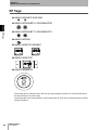
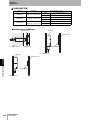
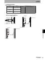
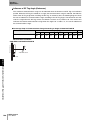
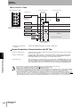
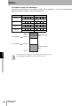
Access Address Setting Switches
Use these switches to set the memory address for reading data.
Item
Description
Setting Specify the memory address of the RF Tag in 4-digit hexadecimal.
method Example to specify an RF Tag memory address of 01A3 hex:
“0“
Section 2 ID Flag Sensor
“1“
“A“
“3“
Refer to the following figure for a set position
of the Setting Switch.
Cutting edge
Setting
range
0000 to FFFF hex (See note.)
Default setting: 0000 hex
Note: The upper 8 bits will not be read if FFFF hex is specified for a16-bit read/
write operation. All output bits will be OFF.
Example) When it sets "B".
The setting of the access address setting switches is read only when the power supply is turned ON.
Therefore, settings cannot be changed while the power is being supplied. Turn OFF the power supply before changing
the settings.
Antenna Connector
Connect this connector to the V680-series Antenna (described in this User's Manual).
1
2
22
RFID System
User's Manual
Pin No.
Name
1
S
2
GND
Description
I/O
Signal line
---
Analog ground
---
Section 2
Names and Functions of Components
Antennas
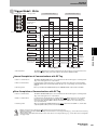
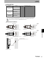
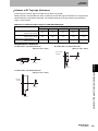
V680-HS51
(2) Communications sufrace
(3) Ferrite core
Section 2 Antennas
(4) Connector
V680-HS52
(2) Communications sufrace
(1) Operation indicator
(3) Ferrite core
(4) Connector
V680-HS63
(2) Communications sufrace
(3) Ferrite core
(4) Connector
(1) Operation indicator
V680-HS65
(2) Communications sufrace
(1) Operation
indicator
(3) Ferrite core
(4) Connector
No.
Name
Description
1
Operation indicator
Lights when a signal is transmitted.
2
Communication surface
Mounted facing the RF Tags.
3
Ferrite core
4
Connector
Connects to the ID Flag Sensor.
RFID System
User's Manual
23
Section 2
Names and Functions of Components
RF Tags
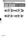
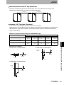
V680-D1KP52MT/-D2KF52M
Section 2 RF Tags
V680-D1KP52M-BT01/-D2KF52M-BT01
V680-D1KP52M-BT11/-D2KF52M-BT11
V680-D1KP53M
V680-D1KP66T/D1KP66MT
V680-D1KP66T-SP
V680-D1KP58HTN
The ID Flag Sensor communications with the RF Tags through the Antenna to read and write data in
the internal memory of the RF Tags.
The printed side is the communications surface. Mount the RF Tags with the communications surfaces
facing the Antenna.
24
RFID System
User's Manual
Section 2
Names and Functions of Components
V680-D8KF67/-D8KF67M
Section 2 RF Tags
V680-D8KF68/-D32KF68
V680S-D2KF67/-D2KF67M
V680S-D2KF68/-D2KF68M
V680S-D8KF67/-D8KF67M
V680S-D8KF68/-D8KF68M
The ID Flag Sensor communications with the RF Tags through the Antenna to read and write data in
the internal memory of the RF Tags.
The printed side is the communications surface. Mount the RF Tags with the communications surfaces
facing the Antenna.
RFID System
User's Manual
25
Section 2
Names and Functions of Components
MEMO
Section 2 RF Tags
26
RFID System
User's Manual
Section 3
Functions
Optional Functions
30
Wire-saving Mode
32
Parity Check
33
Address Shift
34
Noise Measurement
35
Write Protection
36
RFID System 27
User's Manual
Functions
28
Section 3
Communications Mode
Section 3
Functions
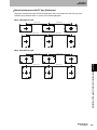
Communications Mode
The ID Flag Sensor operates after reading the setting of the mode setting switches when the power supply is
turned ON. Set the mode for communications with the RF Tags or set the Noise Measurement Mode on the
access mode setting switch. There are three communications modes, each with different timing for completing
communications with RF Tags: Mode 1, Mode 2, and Mode 3. Also, each of these modes has two other modes
to specify when to start communications with the RF Tags: Trigger Mode and Auto Mode. Mode 2 and Mode 3
are compatible with the V600 series.
Section 3 Communications Mode
Communications end
timing
Communications start Access mode setting
timing
switch
Mode overview
Mode 1
Trigger Mode1
0: SYNC1
Standard modes
Auto Mode1
1: AUTO1
Mode 2
Trigger Mode2
2: SYNC2
Auto Mode2
3: AUTO2
Trigger Mode3
4: SYNC3
Auto Mode3
5: AUTO3
Mode 3
Compatible with V600-HAR91/81 and HAM91/81.
Compatible with V600-HAR92.
Some of the functions supported in Mode 1 cannot be used in the V600-compatible modes.
For details, refer to V600-Compatible Mode.
p.208
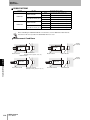
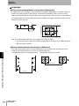
Trigger Mode
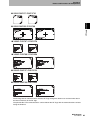
In Trigger Mode, an RF Tag on a workpiece or pallet in the interrogation zone of the Antenna is
detected by a sensor or a switch. A control signal (called the trigger signal) is output from the PLC to
the ID Flag Sensor to trigger the ID Flag Sensor to begin communications with the RF Tag. The ID Flag
Sensor reads the RF Tag data and outputs the results to the PLC.
PLC
V680-A60
Interface Cable
V680-series
RF Tag
V680-HAM91/V680-HAM81
ID Flag Sensor
V680-series
Antenna
Pallet
Sensor or Switch
Only one Interface Cable (I/O connector CN1) is used to read RF Tag data. The address shift, noise check, and parity
check functions, however, are not possible when only CN1 is used.
28
RFID System
User's Manual
Section 3
Functions
Auto Mode
In Auto Mode, the ID Flag Sensor automatically begins communications with a RF Tag on a workpiece
or pallet when it enters the interrogation zone of the Antenna, and then the ID Flag Sensor outputs the
result to the PLC.
PLC
Section 3 Communications Mode
V680-A60
Interface Cable
V680-HAM91/V680-HAM81
ID Flag Sensor
V680-series
Antenna
V680-series
RF Tag
Pallet
Only one Interface Cable (I/O connector CN1) is used to read RF Tag data. The address shift, noise check, and parity
check functions, however, are not possible when only CN1 is used.
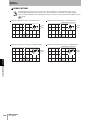
Noise Measurement
The Noise Measurement Mode can be used to check if there is noise around the Antenna that is
affecting communications with the RF Tag. When the power supply is turned ON with the access mode
switch set to this mode, the noise around the Antenna will be measured and the result will be displayed
on indicators and output to external outputs.
Noise measurement can performed with the above mode setting or by turning ON the NOISE_IN external input when
Trigger Mode 1 or Auto Mode 1 is being used. For details, refer to Trigger Mode1 :Noise Measurement.
p.67
RFID System
User's Manual
29
Section 3
Functions
Optional Functions
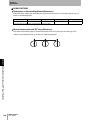
The following optional functions can be enabled by using the mode setting switches (access mode setting,
output mode setting, read mode setting, or write mode setting) and specifying the control signal.
Function
Description
Output time operation
Specified by setting the output mode.
Verification
Set the read mode to "VERIFY".
Wire saving
Set the read mode to "DATA READ2".
Section 3 Optional Functions
Write mode
Specified by setting the write mode.
Write protection
Specified using the WRITE_PROTECT external input.
Address shift
Specified using theADR0 to ADR2 external inputs.
Noise check
Specified using the NOISE_IN external input.
Output Time Operation
Set the output method and time for the normal completion output (NORMAL/STRB), error completion
output (ERR), and data outputs (OD0 to OD15). There are two output methods: OFF delay and fixed
time.
RF Tag position
Fixed time
output
OFF delay
Out of communications
range
ON
OFF
In communications
range
Out of communiIn communications
cations range
Out of communications range
range
Fixed output time
Fixed output time
t1 ms
t1 ms
ON
OFF
t2 ms
OFF delay
t2 ms
OFF delay
• The output time operation specification depends on the communications mode. A setting error will
occur if an output method that is not supported is set
Communications mode
Standard modes Trigger Mode 1
Auto Mode 1
Output method specification
Output rotary switch setting range
Designation not required.
(See note1.)
Either from "0" to "9"
OFF delay
10 ms(“0“)/50 ms(“1“)/500 ms(“2“) OFFDELAY
V600-compatible Trigger Mode 2
modes
Auto Mode 2
Fixed time
10 ms(“3“)/50 ms(“4“)/CONTINUOUS(“5“) (See note2.)
Fixed time
10 ms(“3“)/50 ms(“4“)/CONTINUOUS(“5“) (See note2.)
Trigger Mode 3
OFF delay
10 ms(“0“)/50 ms(“1“)/500 ms(“2“) OFFDELAY
Auto Mode 3
OFF delay
10 ms(“0“)/50 ms(“1“)/500 ms(“2“) OFFDELAY
Note1. : The output will continue in Trigger Mode 1 until the trigger input turns OFF.
2. : When it is set to "CONTINUOUS" at the FIXED TIME OUTPUT, it keeps OUTPUT until INHIBIT/TRIG input turns to
OFF.
For detail timing of output time, refer to Section 5 Control I/O Interface, and Section 7 Appendices when using V600
compatible mode.
p.60, p.208
30
RFID System
User's Manual
Section 3
Functions
Verification
The verification function compares the data (16 bits) that is input to the external data input lines (ID0 to
ID15) with the actually data (16 bits) read from the RF Tag, and outputs the result to indicate whether
the data matches or not. The result of the verification is output to the external data outputs (OD0:
Match, OD7: Mismatch, OD1 to OD6 and OD8 to OD15: Not used.) The result can also be checked on
the Data Display LED on the ID Flag Sensor.
Wire-saving Mode
The Wire-saving Mode enables reading data and detecting errors using only 16 external data outputs
Section 3 Optional Functions
(OD0 to OD15). Control can be performed using one 16-point I/O Unit in a Programmable Controller.
For details, refer to Wire-saving Mode.
p.32
Write Mode
Specify the method for writing data to the RF Tag. Specify the mode to write 2 bytes (16 bits) or 1 byte
(8 bits) at a time, or specify the mode to set or clear specified bits.
Write Protection
Write protection can be enabled to prevent product model numbers, model names, or other important
data saved in RF Tags from being lost.
For details, refer to Write Protection.
p.36
Address Shift
The address set on the access address setting switches can be offset by the value specified by
external data inputs ADR0 to ADR2. This function is useful for reading more 16 bits (2 bytes) of RF Tag
data.
For details, refer to Address Shift.
p.34
Noise Measurement
This function can be used to check if there is noise around the Antenna that is affecting
communications with the RF Tag. The noise measurement when you turn ON the NOISE_IN external
input in Sync Mode 1 or Auto Mode 1. The operating mode called Noise Measurement Mode by setting
the access mode setting switch to "6" is for measuring noise at startup.
For details, refer to Noise Measurement.
p.35
RFID System
User's Manual
31
Section 3
Functions
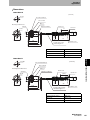
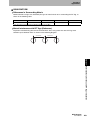
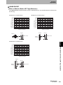
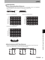
Wire-saving Mode
The Wire-saving Mode enables detecting read data signals and normal/error completion signals using only 16
data outputs (OD0 to OD15). Using this mode enables controlling reading 16-bit data using only one 16-point
Input Unit for a PLC or a wire-saving device.
System Configuration Example: Combination and Usage of I/O Lines in Each Mode
• Normal Read Wiring: DATA READ 1
• Wire-saving Read Wiring: DATA READ 2
Section 3 Wire-saving Mode
Number of Required I/O
Number of Required I/O
Output Units: 1
Output Units: 1
Input Units: 2
Input Units: 1
Output Unit
Input Unit
Output Unit
Input Unit 1
Input Unit 2
INHIBIT/TRIG
NORMAL/STRB, ERR,
PARITY (3 points)
OD0 to OD15 (16 points)
INHIBIT/TRIG
V680-HAM91/
V680-HAM81
OD0 to OD15 (16 points)
V680-HAM91/V680-HAM81
• For Wire-saving Mode, outputting all zeros on the data lines (0000 hex) is used as communications
control, and outputting all ones on the data lines (FFFF hex) is used as an error completion output.
Normal completion (NORMAL/STRB) is detected by confirming that the output from the data lines is
not all zeros (0000 hex) and not all ones (FFFF hex).
• All zeroes (0000 hex) and all ones (FFFF hex) cannot be used as data when Wire-saving Mode is
used.
• Error codes cannot be output when an error completion occurs. The data indicators, however, will
flash red to show the error code.
• The parity output is not connected and cannot be used.
• The Wire-saving Mode cannot be used when Trigger 2 or Auto 2 Mode is used. Attempting to do so
will result in a settings error.
32
RFID System
User's Manual
Section 3
Functions
Parity Check
This function detects vertical parity in the data output on the data output lines (OD0 to OD15) and outputs the
parity status. If the number of bits that are ON in the data output lines is even, then the parity output is OFF. If
the number of bits that are ON in the data output lines is odd, then the parity output is ON. The parity check is
performed for output data on the cable communications between the host device and the ID Flag Sensor. The
parity check can be used to effectively perform simple checks for disconnected cables or wiring.
The parity check cannot be used in Trigger Mode 2 or Auto Mode 2. The ID Flag Sensor indicates a Setting Error.
Section 3 Parity Check
p.208
RFID System
User's Manual
33
Section 3
Functions
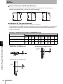
Address Shift
The address set on the access address setting switches can be offset by the value specified by external data
inputs ADR0 to ADR2 to change the access address. The address shift enables reading or writing to up to 16
access address (up to 128 bits) of RF Tag memory.
Address Specification Example with 8-kilobyte RF Tag
0000 hex
Section 3 Address Shift
Conditions: Access address setting switch setting = 0ED5 hex
Address shift input = 4 (ADR2 = 1, ADR1 = 0, ADR0 = 0)
Access address: 0EDD hex
0ED5 hex
0ED6 hex
0ED7 hex
0ED8 hex
0ED9 hex
0EDA hex
0EDB hex
0EDC hex
0EDD hex
1
Access address set on access address setting switches
2
+ address shift (= 4)
3
4
Access address in RF Tag
0EDE hex
0EDF hex
0EE0 hex
1FFF hex
Note 1. An address error will occur if the address shift exceeds the maximum address setting (FFFF hex).
Example of Address Error
Access address setting switches:
FFFD hex
Address shift input:
5 (ADR2 = 1, ADR1 = 0, ADR0 = 1)
Access address:
Address error
2. The address will be shifted by blocks when the 1-Byte Write Mode is used.
Access address setting switches:
0010 hex
Address shift input:
3 (ADR2 = 0, ADR1 = 0, ADR0 = 1)
Access address:
0013 hex
The address shift function can be used only in Trigger 1 or Auto 1 Mode.
34
RFID System
User's Manual
Section 3
Functions
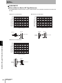
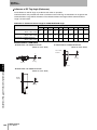
Noise Measurement
You can check whether noise that affects communications with RF Tags exists in the area where the Antenna
and ID Flag Sensor are installed.
In Trigger Mode 1 or Auto Mode 1, noise measurement is performed by turning ON the NOISE_IN external
input. The result of noise measurement will be output to the external data outputs when the NORMAL/STRB
signal is turned ON after the measurement is performed.
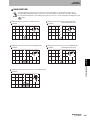
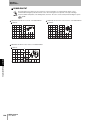
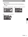
The output will be on a scale of 00 to 99 for the strength of the noise affecting the Antenna. The external data
output lines will output the value converted to hexadecimal. The measured noise strength is also displayed in
Section 3 Noise Measurement
eight levels on the Data Display LED, and so it can be checked directly on the ID Flag Sensor.
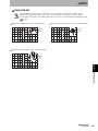
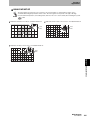
Relation between Result Output and Data Display LED
Result output
“00” to “10
“11” to “21
“22” to “32
“33” to “43
“44” to “54
Data indicator status
7
2
1
0
15 14 13 12 11 10
9
8
2
1
0
15 14 13 12 11 10
9
8
2
1
0
15 14 13 12 11 10
9
8
2
1
0
15 14 13 12 11 10
9
8
2
1
0
15 14 13 12 11 10
9
8
7
7
7
7
6
6
6
6
6
5
5
5
5
5
4
3
4
3
4
3
4
3
4
3
Data indicator status
Result output
7
“55” to “65
1
0
15 14 13 12 11 10
9
8
2
1
0
15 14 13 12 11 10
9
8
2
1
0
15 14 13 12 11 10
9
8
2
1
0
15 14 13 12 11 10
9
8
7
“77” to “87
7
“88” to “99
OFF
2
7
“66” to “76
6
6
6
6
5
5
5
5
4
4
4
4
3
3
3
3
:ON(Green)
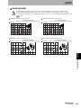
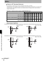
Example of Results Output and Influence on Communications Range
The values given for the influence of the noise level obtained from noise measurement and the communications range
are for reference only. The results depend on the type of Antenna and RF Tag used, and differences in the noise
environment. Be sure to check carefully when installing the system.
Communications range
(noise level 0 to 100%)
100%
80%
60%
40%
20%
0%
0
10
20
30 40 50
Noise level
60
70
Measurement Conditions
Antenna
: V680-HS63
RF Tag
: V680-D1KP66T(non-metallic mounting)
Command
4-byte write
RFID System
User's Manual
35
Section 3
Functions
Write Protection
The write protection function protects important data stored in the memory of a RF Tag, such as the product
model or type, from being overwritten inadvertently.
Enable the write protection function after writing important data as described in this section.
Setting Write Protection
For the write protection function to be effective, it must be enabled in both the ID Flag Sensor settings
and the RF Tag settings.
Section 3 Write Protection
Write protect enable/disable settings is effective only TRIGGER MODE 1 and AUTO MODE 1.
Write protect is always enabled at the TRIGGER MODE 2 and AUTO MODE 2.
The method of write protect for TRIGGER MODE 2 and AUTO MODE 2 confirms to the V600 series.
Details of Write Protect function for V600-compatible Mode, refer to the Section 7 Appendices
p.219
1. Enabling the Write Protection in the ID Flag Sensor
Write protection can be enabled by turning OFF pin 6 (NOISE_IN/WRITE PROTECT) of I/O connector CN2.
NOISE_IN/WRITE PROTECT input is effective as WRITE PROTECT input only when it specified write mode(R/W : ON).
2. Setting Write Protection for RF Tags
Write protection is set in the 4 bytes from RF Tag addresses 0000 hex to 0003 hex. Write protection for RF Tags is enabled in the
most significant bit of address 0000 hex.
Write-protect Bit (most significant bit of address 0000 hex)
1: Write-protected (write protection enable)
0: Not write-protected (write protection disable)
Memory Map for RF Tag Write Protection Settings
Address
0000 hex
Bit
7
6
Enable/
disable
5
4
3
2
1
0
Upper two digits of start address (00 to 7F)
0001 hex
Lower two digits of start address (00 to FF)
0002 hex
Upper two digits of end address (00 to FF)
0003 hex
Lower two digits of end address (00 to FF)
When write protection is not used, the above addresses can be used as user memory. If it is used as user memory,
disable the write protection function of the ID Flag Sensor by turning ON pin 6 (NOISE_IN/WRITE PROTECT) of I/O
connector CN2. NOISE_IN/WRITE PROTECT input must be OFF when reading the RF Tag. If it turns ON during
reading operation, the ID Flag Sensor execute Noise level measurement.
Addresses in RF Tag Memory That Can Be Write Protected
Start address: 0000 hex to 7FFF hex
End address: 0000 hex to FFFF hex
The write-protection setting area of the RF Tag cannot be write-protected.
36
RFID System
User's Manual
Section 3
Functions
Example of Write Protection
Start Address Is Lower Than the End Address
The memory area between the start address and end address will be write-protected.
0000 hex
Address
(hex)
Bit
Upper digits
Lower digits
0015 hex
1
0000
0
0
0
0
0
8
0
0001
0
0
1
0
1
0
0
0
1
0
1
0
0
0120 hex
5
0
0
0
0
1
0
0
0
0
0003
0
Write-protected
Section 3 Write Protection
0
0
0
1
0002
0
1
2
0
03E7 hex
Start Address Is Equal to End Address
Only the selected address (one byte) will be write-protected.
0000 hex
Address
(hex)
Bit
Upper digits
1
0000
0
0
Lower digits
0
0
0
8
0
0
0
1
0
0
0
1
0
0021 hex
0001
0
0
0
0
0
0
1
0
0
0
0
0
0
0
1
0
0
0
2
0002
1
0
0003
Write-protected
0
2
1
03E7 hex
End Address Is Higher than the Last RF Tag Address
The memory area between the start address and the last RF Tag address will be write-protected.
0000 hex
Address
(hex)
0000
0001
0002
0003
Bit
Upper digits
1
0
0
Lower digits
0
0
0
8
0
0
0
1
1
0
0
0
0
0
0
1
1
1
1
0
0
0
0
0
1
1
1
1
0
F
1
3
0
0
1
3
0300 hex
Write-protected
F
03E7 hex
RFID System
User's Manual
37
Section 3
Functions
Start Address Is Higher Than End Address
The memory area between the start address and the last RF Tag address, as well as the area between
0004 hex and the end address will be write-protected.
Address
(hex)
0000
0001
Section 3 Write Protection
0002
0003
Bit
Upper digits
1
0
0
0
0
0
Lower digits
0
0
0
0
1
0
0
0
0
0
0
0
8
0
0
0
0
0
1
0
0
0
1
1
2
0
0
0
0
1
0
1
1
5
0000 hex
0004 hex
Write-protected
End address
0015 hex
Start address
0120 hex
Write-protected
03E7 hex
Disabling Write Protection
Disabling Write Protection for Part of the RF Tags
Set the uppermost bit of 0000 hex to 0.
Disabling All Write Protection for the Whole RFID system
Turn ON pin 6 (NOISE_IN/WRITE PROTECT) of the I/O connector on the ID Flag Sensor.
Caution When Using Write Protection:
The write protection function is an OMRON ID Flag Sensor function. It cannot be used with RFID reader/writer
manufactured by other companies.
Write protect enable/disable settings is effective only TRIGGER MODE 1 and AUTO MODE 1.
Write protect is always enabled at the TRIGGER MODE 2 and AUTO MODE 2.
TRIGGER MODE 3 and AUTO MODE 3 is not supported Write function itself.
38
RFID System
User's Manual
Section 4
Installation, Connections, and Wiring
40
Installing Antennas
45
Installing RF Tags
48
Section 4
ID Flag Sensor
Installation, Connections, and Wiring
RFID System
User's Manual
39
Section 4
Installation, Connections, and Wiring
ID Flag Sensor
Installation
To ensure full functionality of the ID Flag Sensor, follow the instructions provided in this section for
installation.
Installation Site
Do not install the ID Flag Sensor in the following locations.
• Locations exposed to ambient temperatures that are not between 10 and 55C or where there are
radical temperature changes resulting in condensation
• Locations exposed to humidity that is not between 25% and 85%
• Locations subject to corrosive gas, flammable gas, dust, salt, or metal powder
Section 4 ID Flag Sensor
• Locations that will expose the ID Flag Sensor to direct vibration or shock
• Locations exposed to direct sunlight
• Locations exposed to spray of water, oil, or chemicals
• Locations more than 2,000 m above sea level
Mounting in a Panel
The ID Flag Sensor can be used at an ambient temperature range of 10 to 55C. Be sure to observe
the following precautions.
• Make sure that the Unit is provided with sufficient ventilation space.
• Do not install the Unit close to heaters, transformers, or large-capacity resistors that radiate excessive
heat.
40
RFID System
User's Manual
Section 4
Installation, Connections, and Wiring
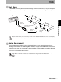
Installation Method
The ID Flag Sensor is to be mounted to a DIN Track. Mount the DIN Track, and then mount the ID Flag
Sensor to the DIN Track.
1. First hook the ID Flag Sensor Unit to part A, then press it in direction B to mount it to the DIN Track.
2. To disconnect the ID Flag Sensor Unit from the DIN Track, pull the mounting hook downwards, and
then lift the Unit upwards.
DIN Track
Mounting Hook
End Plate
End Plate
Section 4 ID Flag Sensor
Mounting Hook
A
DIN Track
PFP-100N2 (OMRON)
End Plate
PFP-M (OMRON)
B
Attaching the End Plates:
To mount an End Plate easily, first hook the bottom of the End Plate and then hook the
top on the DIN Track, pull the End Plate downwards and tighten the screw.
Recommended tightening torque: 1.2 Nm.
Mounting Interval
The ID Flag Sensor Units will generate heat if they are mounted side-byside.
Leave space between Units of at least 10 mm.
10 mm min.
10 mm min.
End Plate
End Plate
Spacer
Spacer
Use at least 2 OMRON DIN Track Spacers. (Each Spacer is 5 mm wide)
Spacer
PFP-S
RFID System
User's Manual
41
Section 4
Installation, Connections, and Wiring
Connection and Wiring
Interface Cable
INPUT/OUTPUT controls
• When using a solid-state output with the maximum switching current rating over 1A , there is a
possibility of causing External Input Errors due to the delay of rise /fall time of output signal.
Consider this when selecting the solid-state output.
• When using a contact output, consider chattering and the minimum switching current.
• When connecting an inductive load or an electrical device that tends to generate noise to the output,
connect a diode in parallel with the load. Connect the cathode side of the diode to the positive side of
the power supply.
WARNING
Section 4 ID Flag Sensor
Power Supply Voltage
• Do not impose an AC(100VAC to 240VAC) power supply or any voltage exceeding the rated voltage
range on the V680-HAM91/-HAM81. Unsuitable power supplies may cause the V680-HAM91/HAM81 to explode or bum.
Load Short-circuiting
• Do not short-circuit the load connected to the V680-HAM91/-HAM81 or connect power to the load.
Any of these may cause the V680-HAM91/-HAM81 to explode or bum.
WARNING
• Do not mis-wire and do not reverse polarity of the power supply connected to the V680-HAM91/HAM81. Wiring mistakes, including reversed power supply polarity may cause the V680-HAM91/HAM81 to explode or bum.
42
RFID System
User's Manual
Section 4
Installation, Connections, and Wiring
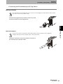
Connecting and Disconnecting the ID Flag Sensor
Mounting Procedure
Line up the direction of the triangle mark on the connectors of the ID Flag Sensor and the interface cable, and then
press in the connector of the interface cable.
The lock will engage when the interface cable is pressed
into the connector on the ID Flag Sensor.
Section 4 ID Flag Sensor
Removal Procedure
To remove the connector of the interface cable, always hold the connector and pull it out in a straight line.
Pulling the cable may result in severing the cable or other product failure.
Unlock the connector on the ID Flag Sensor and pull out
the connector of the interface cable.
RFID System
User's Manual
43
Section 4
Installation, Connections, and Wiring
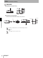
Antenna Connector
Mounting the Antenna
1. Hold the connector part of the Antenna and insert it into the
Antenna port while matching the key on the ID Flag Sensor with
the groove on the connector.
Key
Antenna connector
Section 4 ID Flag Sensor
2. Turn the connector clockwise to lock it in place.
Removing the Antenna
1. Turn the connector in counterclockwise to release the lock.
2. Pull the connector straight out of the port.
Key
Antenna connector
The connector cannot be removed without turning it to release the lock.
If the cable is pulled without releasing the lock, it may cause the cable or wires to break. Make sure that the lock is
released before pulling out the connector.
44
RFID System
User's Manual
Section 4
Installation, Connections, and Wiring
Installing Antennas
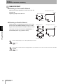
V680-HS51
Install the Antenna using the nuts and toothed washer that are provided on both sides of the mounting
material, as shown in the diagram below.
Metallic material
Mounting Hole Dimensions
Nut
Antenna
12
+0.5
0
dia.
Toothed washer
Section 4 Installing Antennas
For details on installing Antennas, refer to Antenna Mounting Precautions.
p.151
Securely tighten the screws to a torque of 6 Nm.
V680-HS52
Install the Antenna using the nuts and toothed washers that are provided on both sides of the mounting
material, as shown in the diagram below.
When the Antenna is mounted to a metallic material, the communications range will be reduced by approximately 10%
compared with mounting to a non-metallic material.
For details on the effect of metal surrounding the Antenna, refer to Antenna Mounting Precautions.
p.151
Non-metallic material
Mounting Hole Dimensions
Nuts
Antenna
22
+0.5
0
dia.
Toothed washers
Securely tighten the screws to a torque of 40 Nm.
RFID System
User's Manual
45
Section 4
Installation, Connections, and Wiring
V680-HS63
Installation from the Front
Two, M4
Coil center
28±0.2
40
27
53
5
Installation from the Back
Insert the nuts that come with the Antenna into sections A.
Section 4 Installing Antennas
Two, 4.5 dia.
Coil center
Nut
A
40
28±0.2
27
For details on installing Antennas, refer to Antenna Mounting Precautions.
p.151
Securely tighten screws to a torque of 1.2 Nm.
46
RFID System
User's Manual
Section 4
Installation, Connections, and Wiring
V680-HS65
100
Use M4 screws and spring washers (in four places) for
Four, M4
90±0.2
Antenna installation.
100
90±0.2
Section 4 Installing Antennas
Securely tighten screws to a torque of 0.7 to 1.2 Nm.
Mounting Bracket Dimensions (Provided Only with the V680-HS65)
Note: When installing the Antenna, mount it on the
100±0.2
90±0.1
Four, C1
enclosed Mounting Bracket. The Mounting Bracket
is not necessary, however, if the Antenna is
mounted on a metal base that is larger than the
Antenna (100 100 mm).
100±0.2
90±0.1
Mounting base
Four, 4.5+0.3 dia.
V680-HS65
0
Mounting Bracket
(provided)
For details on installing Antennas, refer to Antenna Mounting Precautions.
p.151
RFID System
User's Manual
47
Section 4
Installation, Connections, and Wiring
Installing RF Tags
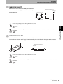
V680-D1KP52MT
RF Tag Installation Direction
Mount the RF Tags as shown in the diagram on the right. The
R0.2 max.
epoxy adhesives listed in the following table are recommended
for the given temperature ranges.
40 to 70C
Section 4 Installing RF Tags
40 to 150C
8.1+0.1 dia.
0
Ambient operating
temperature
Product name
Manufacturer
Two-part Epoxy-compound
Resin: TB2001 (main agent)/
TB2105C (curing agent)
Three Bond Co., Ltd.
One-part Moisture-curing
Elastic Adhesive
TB1530
Three Bond Co., Ltd.
One-part Epoxy Resin: TB2285
Three Bond Co., Ltd.
Two-part Epoxy Resin: TB2087
Three Bond Co., Ltd.
5+0.1
0
Marked side
Marked side
When installing RF Tags, refer to RF Tag Mounting Precautions.
p.155
When embedding the V680-D1KP52MT into a metal surface, use the V680-HS51/-HS52 Antenna.
Communications will not be possible if the V680-HS63 Antenna is used.
Refer to Differences in Surrounding Metals (Reference)in Section 7 Appendices for information on the effect of metal
behind the V680-D1KP52MT.
p.155
V680-D1KP52M-BT01/-D1KP52M-BT11
RF Tag Installation Direction
1. Turn the RF Tag clockwise, attach to the Mounting holes.
RF Tag
V680-D1KP52M-BT01 is attached to the mounting holes in the M10,
V680-D1KP52M-BT11 to the mounting holes in the M8.
Mounting Hole
2. Secure by tightening the bolts of the RF Tag.
RF Tag
When mounting the RF Tags, tighten the bolts to the following torques.
V680-D1KP52M-BT01: 24.5 Nm
V680-D1KP52M-BT11: 11 Nm
48
RFID System
User's Manual
Section 4
Installation, Connections, and Wiring
V680-D1KP53M
RF Tag Installation Direction
Mount the RF Tags as shown in the diagram on the right. The
V680D1KP53M
R0.5 max.
epoxy adhesives listed in the following table are
recommended for the given temperature ranges.
Ambient operating
temperature
Product name
Two-part Epoxy-compound
Resin: TB2001 (main agent)/
TB2105C (curing agent)
40 to 70C
10+0.09 dia.
0
Three Bond Co., Ltd.
4.6+0.2
0
One-part Moisture-curing
Elastic Adhesive
TB1530
Three Bond Co., Ltd.
One-part Epoxy Resin: TB2285
Three Bond Co., Ltd.
Two-part Epoxy Resin: TB2087
Three Bond Co., Ltd.
Marked side
Section 4 Installing RF Tags
40 to 150C
Manufacturer
Marked side
When installing RF Tags, refer to RF Tag Mounting Precautions.
p.155
When embedding the V680-D1KP53M into a metal surface, use the V680-HS51/-HS52 Antenna.
Communications will not be possible if the V680-HS63 Antenna is used.
Refer to Differences in Surrounding Metals (Reference)in Section 7 Appendices for information on the effect of metal
behind the V680-D1KP53M.
p.158
RFID System
User's Manual
49
Section 4
Installation, Connections, and Wiring
V680-D1KP66T
Mounting on Non-metallic Material
Mount the RF Tag using M3 pan-head screws from the
Mounting Hole Dimensions
marked side.
Two, M3
Tightening torque: 0.3 to 0.5 Nm
M3 pan-head screw
25±0.2
Marked side
25±0.2
Mounting on Metallic Material
Communications range will decrease if there is metal
M3 pan-head screw
Section 4 Installing RF Tags
on the back of the V680-D1KP66T RF Tag. If the RF
Mounting Hole Dimensions
Marked
side
Tag is to be used mounted to metallic material, use the
Two, M3
separately sold special attachment (V600-A86) or a
non-metallic spacer (e.g., plastic or resin).
25±0.2
25±0.2
Attachment (V600-A86)
When installing RF Tags, refer to RF Tag Mounting Precautions.
p.155
Refer to Effect of Metal on Back of RF Tags (Reference) for information on the effect of metal on the back of the V680D1KP66T.
p.160
50
RFID System
User's Manual
Section 4
Installation, Connections, and Wiring
V680-D1KP66MT
Mount the RF Tag to metal using M3 pan-head screws
Mounting Hole Dimensions
from the marked side. Tighten the screws to a torque
Two, M3
of 0.3 to 0.5 Nm..
M3 pan-head screw
25±0.2
Marked side
25±0.2
When installing RF Tags, refer to RF Tag Mounting Precautions.
Section 4 Installing RF Tags
p.155
Refer to Effect of Surrounding Metals (Reference) for information on the effect of metal on the back of the V680D1KP66MT.
p.162
V680-D1KP66T-SP
Mount the RF Tag using M5 screws and washers. Tighten the screws to a torque of 1.2 Nm.
The installation direction of RF Tags is not restricted by the travel direction in respect to the Antenna.
Mounting Hole Dimensions
Two, M5
80±0.2
When installing RF Tags, refer to RF Tag Mounting Precautions.
p.155
Refer to Effect of Metal on Back of RF Tags (Reference) for information on the effect of metal on the back of the V680D1KP66T-SP.
p.164
RFID System
User's Manual
51
Section 4
Installation, Connections, and Wiring
V680-D1KP58HTN
RF Tag Installation Direction
The RF Tags have a limited life span. Therefore, install them in locations in which they can be easily
replaced. Use the following procedure to mount the V680-A80 Attachment when required.
1. Mount the Attachment to the workpiece.
M12
Section 4 Installing RF Tags
Mounting Hole Dimensions
2. Tighten the lock nut.
Use a tightening torque of 21 to 42 N·m.
3. Mount the RF Tag to the Attachment.
The RF Tag can be mounted in either
direction.
Insert the split pin into the 3.2-dia. hole and open the tip of the pin to secure.
Two nuts and one split pin are provided with the V680-A80 Attachment. Replacement split pins must be
provided by the user.
Split pin
52
RFID System
User's Manual
Nominal: 3.2 mm 20 mm (length)
Section 4
Installation, Connections, and Wiring
V680-D2KF52M
RF Tag Installation Direction
R0.2 max.
Mount the RF Tag as shown in the diagram on the right.
The epoxy adhesives listed in the following table are
recommended for the given temperature ranges.
40 to 70C
Product name
Manufacturer
Two-part Epoxy-compound
Resin: TB2001 (main agent)/
TB2105C (curing agent)
Three Bond Co., Ltd.
One-part Moisture-curing
Elastic Adhesive
TB1530
Three Bond Co., Ltd.
5+0.1
0
Marked side
One-part Epoxy Resin: TB2285 Three Bond Co., Ltd.
Two-part Epoxy Resin: TB2087
Three Bond Co., Ltd.
Marked side
Section 4 Installing RF Tags
40 to 85C
8.1+0.1 dia.
0
Ambient operating
temperature
When installing RF Tags, refer to RF Tag Mounting Precautions.
p.155
When embedding the V680-D2KF52M into a metal surface, use the V680-HS51/-HS52 Antenna.
Communciations will not be possible if the V680-HS63 Antenna is used.
Refer to Differences in Surrounding Metals for information on the effect of metal on the back of the V680-D2KF52M.
p.169
V680-D2KF52M-BT01/-D2KF52M-BT11
RF Tag Installation Direction
1. Turn the RF Tag clockwise, attach to the Mounting holes.
RF Tag
V680-D2KF52M-BT01 is attached to the mounting holes in the M10,
V680-D2KF52M-BT11 to the mounting holes in the M8.
Mounting Hole
2. Secure by tightening the bolts of the RF Tag.
RF Tag
When mounting the RF Tags, tighten the bolts to the following torques.
V680-D2KF52M-BT01: 24.5 Nm
V680-D2KF52M-BT11: 11 Nm
RFID System
User's Manual
53
Section 4
Installation, Connections, and Wiring
V680-D8KF67/-D8KF67M
RF Tag Installation Direction
Secure the RF Tag with M3 screws. Tighten the
Mounting Hole Dimensions
screws to a torque of 0.6 Nm.
Two, M3
M3 screw
32±0.2
Marked side
32±0.2
When installing RF Tags, refer to RF Tag Mounting Precautions.
Section 4 Installing RF Tags
p.155
Refer to Effect of Surrounding Metals (Reference) for information on the effect of metal on the back of the V680D8KF67M.
p.174
Refer to Effect of Metal on Back of RF Tags (Reference) for information on the effect of metal on the back of the V680D8KF67.
p.172
V680-D8KF68/-D32KF68
RF Tag Installation Direction
Secure the RF Tag with M4 screws. Tighten the screws to a torque of 0.7 to 1.2 Nm.
Two, M4
M4 screw
Spring washer
44
Flat washer
76
When installing RF Tags, refer to RF Tag Mounting Precautions.
p.155
Refer to Effect of Surrounding Metals (Reference) for information on the effect of metal on the back of the V680D8KF68/-D32KF68.
p.176
54
RFID System
User's Manual
Section 4
Installation, Connections, and Wiring
V680S-D2KF67/-D2KF67M
RF Tag Installation Direction
Secure the RF Tag with M3 screws. Tighten the
Mounting Hole Dimensions
screws to a torque of 0.6 Nm.
Two, M
M3 screw
32±0.2
Marked side
32±0.2
When installing RF Tags, refer to RF Tag Mounting
Precautions.
Section 4 Installing RF Tags
p.155
Refer to Effect of Surrounding Metals (Reference) for information on the effect of metal on the back of the V680SD2KF67M.
p.181
Refer to Effect of Metal on Back of RF Tags (Reference) for information on the effect of metal on the back of the V680SD2KF67.
p.179
V680S-D2KF68/-D2KF68M
RF Tag Installation Direction
Secure the RF Tag with M4 screws. Tighten the screws to a torque of 0.7 to 1.2 Nm.
Two, M4
M4 screw
Spring washer
44
Flat washer
76
When installing RF Tags, refer to RF Tag Mounting Precautions.
p.155
Refer to Effect of Surrounding Metals (Reference) for information on the effect of metal on the back of the V680SD2KF68M.
p.186
Refer to Effect of Metal on Back of RF Tags (Reference) for information on the effect of metal on the back of the V680SD2KF68.
p.183
RFID System
User's Manual
55
Section 4
Installation, Connections, and Wiring
V680S-D8KF67/-D8KF67M
RF Tag Installation Direction
Secure the RF Tag with M3 screws. Tighten the
Mounting Hole Dimensions
screws to a torque of 0.6 Nm.
Two, M
M3 screw
32±0.2
Marked side
32±0.2
When installing RF Tags, refer to RF Tag Mounting Precautions.
Section 4 Installing RF Tags
p.155
Refer to Effect of Surrounding Metals (Reference) for information on the effect of metal on the back of the V680SD8KF67M.
p.191
Refer to Effect of Metal on Back of RF Tags (Reference) for information on the effect of metal on the back of the V680SD8KF67.
p.189
V680S-D8KF68/-D8KF68M
RF Tag Installation Direction
Secure the RF Tag with M4 screws. Tighten the screws to a torque of 0.7 to 1.2 Nm.
Two, M4
M4 screw
Spring washer
44
Flat washer
76
When installing RF Tags, refer to RF Tag Mounting Precautions.
p.155
Refer to Effect of Surrounding Metals (Reference) for information on the effect of metal on the back of the V680SD8KF68M.
p.196
Refer to Effect of Metal on Back of RF Tags (Reference) for information on the effect of metal on the back of the V680SD8KF68.
p.193
56
RFID System
User's Manual
Section 5
Control I/O Interface
I/O Interface Control
58
I/O Control Flow
59
Timing Charts
60
Sample Programming
69
Section 5
Control I/O Interface
RFID System
User's Manual
57
Section 5
Control I/O Interface
I/O Interface Control
The V680-series ID Flag Sensor can be connected to a PLC, I/O Terminal, B7A-series Link Terminal,
DeviceNet device, or other host device. This section describes operations for connecting to and
communicating with these devices.
Overview of Communications Modes
Use the access mode setting switch to set the communications mode for RF Tag communications.
There are three communications modes, each with different timing for completing communications with
RF Tags: Mode 1, Mode 2, and Mode 3. Also, each of these modes has two modes to specify when to
start communications with the RF Tags: Trigger Mode and Auto Mode. Mode 2 and Mode 3 are compatible with the V600.
Section 5 I/O Interface Control
58
Communications end
timing
Communications start Access mode setting Timing
timing
Charts
Mode overview
Mode 1
Trigger
0: SYNC MODE 1
p.60
Standard modes
Auto
1: AUTO MODE 1
p.64
Mode 2
Mode 3
Trigger
2: SYNC MODE 2
p.210
Auto
3: AUTO MODE 2
p.213
Modes compatible with V600-HAR91/81
and V600-HAM91/81
Trigger
4: SYNC MODE 3
p.216
Modes compatible with V600-HAR92
Auto
5: AUTO MODE 3
p.218
Some of the functions supported in Mode 1 cannot be used in the V600-compatible modes.
p.209
RFID System
User's Manual
Section 5
Control I/O Interface
I/O Control Flow
The operation outline for ID Flag Sensor at Trigger Mode 1 and Auto Mode 1 are shown in this page. For detail
timing of ID Flag Sensor , refer to the timing charts in this section. Control the ID Flag Sensor according to the
timing charts.
Trigger Mode
Example: Timing Chart for Trigger Mode 1, and Successful Read
Mode setting switch settings
In communications area
RF Tag position
3. Result cleared
1. Start of communications
INHIBIT/TRIG
2. End of communications
Communications
with RF Tag
Reading
3 ms
NORMAL/STRB
0000 hex
Read data
0000 hex
1. Start of communications
Turn ON the INHIBIT/TRIG input to start communications with the RF Tag after confirming the RF Tag is in the interrogation zone of the Antenna.
2. End of communications
If communications with the RF Tag are completed normally, the ID Flag Sensor will turn
ON the NORMAL/STRB output and will output the read data to the data output bits (OD0
to OD15). The NORMAL/STRB output turns ON 3 ms after the data output lines. Read
the data output after the NORMAL/STRB output turns ON.
3. Clearing results
When you turn OFF the INHIBIT/TRIG input, the NORMAL/STRB output will be turned
OFF, and data output will be cleared to 0000 hex.
Section 5 I/O Control Flow
Data output
(OD0 to OD15: 16 bits)
Auto Mode
Example: Timing Chart for Auto Mode 1, and Successful Read
2. Start of communications
Mode setting switch settings
In communications range
RF Tag position
1. Preparing Communications
INHIBIT/TRIG
3. End of communications
Communications
with RF Tag
4. Result cleared
Reading
OFF delay time
3 ms
NORMAL/STRB
Data output
(OD0 to OD15: 16 bits)
0000 hex
Read data
0000 hex
1. Preparations
Turn OFF the INHIBIT/TRIG input in advance to enable communications.
2. Start of communications
The ID Flag Sensor will start communications with the RF Tag when the RF Tag enters
the interrogation zone of the Antenna.
3. End of communications
If communications with the RF Tag are completed normally, the ID Flag Sensor will turn
ON the NORMAL/STRB output and will output the read data to the data output bits (OD0
to OD15). The NORMAL/STRB output turns ON 3 ms after the data output lines. Read
the data output after the NORMAL/STRB output turns ON.
4. Clearing results
After the RF Tag is out of the interrogation zone of the Antenna, the NORMAL/STRB output and data output bits will be turned OFF after the time set for the OFF delay in the output mode time setting has elapsed.
RFID System
User's Manual
59
Section 5
Control I/O Interface
Timing Charts
Trigger Mode 1: Read
Mode setting switch settings
In communications range
RF Tag position
INHIBIT/TRIG
Communications
with RF Tag
Reading
Reading
R/W input
Access Address : 0010 hex
Address shift input
(ADR0 to 2: 3 bits)
0 hex
Address shift data
3 ms
NORMAL/STRB
3 ms
ERR output
Section 5 Timing Charts
0
Parity
value
0
Parity
value
0
Data output
(OD0 to OD15: 16 bits)
0000 hex
Read
data
0000 hex
Error
code
0000 hex
Data Display LED
(0 to 15: 16 bits)
0000 hex
PARITY output
NOISE_OUT
output
A
Read data display (green)
B
C
D
Normal completion
A. Preparations
E
Error code display (red)
F
G
Completion with error
Before starting communications with the RF Tag, turn OFF the R/W input and set the address shift
input bits (ADR0 to ADR2).
Normal Completion of Communications with RF Tag
B. Start of communications
Turn ON the INHIBIT/TRIG input to start communications with the RF Tag after confirming the RF
Tag is in the interrogation zone of the Antenna.
C. End of communications
If communications with the RF Tag are completed normally, the ID Flag Sensor will turn ON the
NORMAL/STRB output, store the parity value in the PARITY output, and store the read data in the
data output bits (OD0 to OD15). The Data Display LED(0 to 15) corresponding to the read data
will be lit green.
D. Clearing results
When you turn OFF the INHIBIT/TRIG input, the NORM/STRB output will be turned OFF, the parity value (0) will be set on the PARITY output, and the data output bits (OD0 to OD15) will be
cleared to 0000 hex.
Error Completion of Communications with RF Tag
E. Start of communications
Turn ON the INHIBIT/TRIG input to start communications with the RF Tag.
F. End of communications
If communications with the RF Tag are completed with an error(No RF Tag error), the ID Flag Sensor will turn ON ”0” the ERR output, store the parity value in the PARITY output, and store the
error code in the data output bits (OD0 to OD15). The data indicators (0 to 15) corresponding to
the error code will be lit red.
G. Clearing results
When you turn OFF the INHIBIT/TRIG input, the ERR output will be turned OFF “1“, the parity
value (0) will be set on the PARITY output, and the Data Display LED (OD0 to OD15) will be
cleared to 0000 hex.
Wait at least 10 ms after switching the R/W input line before performing next process.
Switch the address shift input (ADR0 to ADR2) at least 10 ms before accessing the RF Tag(e.g., at least 10 ms before turning
ON the trigger input).
Read the data output (OD0 to OD15) after the NORMAL/STRB output turns ON.
60
RFID System
User's Manual
Section 5
Control I/O Interface
Trigger Mode1 : Read with Wire-saving Mode
Mode setting switch settings
In communications range
RF Tag position
INHIBIT/TRIG
Communications
with RF Tag
Reading
Reading
R/W input
Access Address : 0010 hex
Address shift input
(ADR0 to 2: 3 bits)
0 hex
Address shift data
3 ms
NORMAL/STRB
3 ms
ERR output
Parity
value
0
0
Data output
(OD0 to OD15: 16 bits)
0000 hex
Read
data
0000 hex
FFFF hex
Data Display LED
(0 to 15: 16 bits)
0000 hex
0
NOISE_OUT
output
A
Read data display (green)
B
C
D
Normal completion
A. Preparations
E
0000 hex
Error code display (red)
F
G
Completion with error
Section 5 Timing Charts
0
PARITY output
Before starting communications with the RF Tag, turn OFF the R/W input and set the address shift
input bits (ADR0 to ADR2).
Normal Completion of Communications with RF Tag
B. Start of communications
Turn ON the INHIBIT/TRIG input to start communications with the RF Tag after confirming the RF
Tag is in the interrogation zone of the Antenna.
C. End of communications
If communications with the RF Tag are completed normally, the ID Flag Sensor will turn ON the
NORMAL/STRB output, store the parity value in the PARITY output, and store the read data in the
data output bits (OD0 to OD15). The Data Display LED(0 to 15) corresponding to the read data
will be lit green.
D. Clearing results
When you turn OFF the INHIBIT/TRIG input, the NORM/STRB output will be turned OFF, the parity value (0) will be set on the PARITY output, and the data output bits (OD0 to OD15) will be
cleared to 0000 hex.
Error Completion of Communications with RF Tag
E. Start of communications
Turn ON the INHIBIT/TRIG input to start communications with the RF Tag.
F. End of communications
If communications with the RF Tag are completed with an error(No RF Tag error), the ID Flag Sensor will turn ON “0“ the ERR output, store the parity value in the PARITY output, and store FFFF
hex (ON all bits) in the data output bits (OD0 to OD15). The Data Display LED (0 to 15) corresponding to the error code will be lit red.
G. Clearing results
When you turn OFF the INHIBIT/TRIG input, the ERR output will be turned OFF “1“, the parity
value (0) will be set on the PARITY output, and the data output bits (OD0 to OD15) will be cleared
to 0000 hex.
Wait at least 10 ms after switching the R/W input line before performing next process.
Switch the address shift input (ADR0 to ADR2) at least 10 ms before accessing the RF Tag (e.g., at least 10 ms before turning
ON the trigger input).
If communications control will be performed using only data output lines without using the NORMAL/STRB output, for example, implement programming for a timer with a specified time, check the status of each data output line at each specified time,
and read the outputs as data after the data is all zeros or all ones.
All ones and all zeros of data outputs cannot be used as data.
All data output bits will be ON when an error occurs. The Data Display LED (0 to 15) will flash the error code in red corresponding to the occurring error.
RFID System
User's Manual
61
Section 5
Control I/O Interface
Trigger Mode1: VERIFY
Mode setting switch settings
In communications range
RF Tag position
In communications range
INHIBIT/TRIG
Communications
with RF Tag
Verifying
Verifying
Data intput
(ID0 to ID15: 16 bits)
Reference Data
R/W input
Access Address : 0010 hex
Address shift input
(ADR0 to 2: 3 bits)
Address shift data
0 hex
3 ms
3 ms
NORMAL/STRB
ERR output
Section 5 Timing Charts
PARITY output
0
NOISE_OUT
output
Data output
(OD0 to OD15: 16 bits)
0000 hex
Data Display LED
(0 to 15: 16 bits)
All OFF
A
B
0001 hex
0000 hex
Reference data (green)
C
D
E
Reference data and read data match
A, B. Preparations
0000 hex
0080 hex
F
Reference data (green)
G
H
Reference data and read data do not match.
Turn OFF the R/W input before starting communications with the RF Tag, set reference data on
the data input bits (ID0 to ID15), and set the address shift input bits (ADR0 to ADR2).
Reference Data and Read Data Match
C. Start of communications
Turn ON the INHIBIT/TRIG input to start communications with the RF Tag after confirming the RF
Tag is in the interrogation zone of the Antenna.
D. End of communications
If communications with the RF Tag are completed normally, the ID Flag Sensor will turn ON the
NORMAL/STRB output and the data output bit (OD0: data match). The VERIFY OK/NG indicator
will be lit green, and the Data Display LED (0 to 15) corresponding to the reference data will be lit
green.
E. Clearing results
When you turn OFF the INHIBIT/TRIG input, the NORMAL/STRB output and the data output bit
(OD0) will be turned OFF.
Reference Data and Read Data Mismatch
F. Start of communications
Turn ON the INHIBIT/TRIG input to start communications with the RF Tag after confirming the RF
Tag is in the interrogation zone of the Antenna.
G. End of communications
If communications with the RF Tag are completed normally, the ID Flag Sensor will turn ON the
NORMAL/STRB output and the data output bit (OD7: data mismatch). The VERIFY OK/NG indicator will be lit red, and the Data Display LED (0 to 15) corresponding to the reference data will be
lit green.
H. Clearing results
When you turn OFF the INHIBIT/TRIG input, the NORMAL/STRB output and the data output bit
(OD7) will be turned OFF.
Wait at least 10 ms after switching the R/W input line before performing next process.
Switch the address shift input (ADR0 to ADR2) at least 10 ms before accessing the RF Tag(e.g., at least 10 ms before turning
ON the trigger input).
Switch the reference data input (ID0 to ID15) at least 10 ms before accessing the RF Tag(e.g., at least 10 ms before turning
ON the trigger input).
Read the data output(OD0 to OD15) after the NORMAL/STRB output turns ON.
62
RFID System
User's Manual
Section 5
Control I/O Interface
Trigger Mode1: Write
Mode setting switch settings
In communications range
In communications range
RF Tag position
INHIBIT/TRIG
Communications
with RF Tag
Write
failed
Writing
Data intput
(ID0 to ID15: 16 bits)
Access Address : 0010 hex
Write data
R/W input
Address shift input
(ADR0 to 2: 3 bits)
0 hex
Address shift data
3 ms
NORMAL/STRB
3 ms
ERR output
0
1
0000 hex
Error
code
0
NOISE_OUT
output
Data output
(OD0 to OD15: 16 bits)
Data Display LED
(0 to 15: 16 bits)
All OFF
A
B
D
E
Normal completion
A, B. Preparations
Error code display (red)
Write data display (green)
C
F
0000 hex
G
H
Section 5 Timing Charts
PARITY output
Completion with error
Turn ON the R/W input before starting communications with the RF Tag, set the write data on the
data input bits (ID0 to ID15), and set the address shift input bits (ADR0 to ADR2).
Normal Completion of Communications with RF Tag
C. Start of communications
Turn ON the INHIBIT/TRIG input to start communications with the RF Tag after confirming the RF
Tag is in the interrogation zone of the Antenna.
D. End of communications
If communications with the RF Tag are completed normally, the ID Flag Sensor will turn ON the
NORMAL/STRB output, and the Data Display LED (0 to 15) corresponding to the write data will be
lit green.
E. Clearing results
When you turn OFF the INHIBIT/TRIG input, the NORMAL/STRB output will be turned OFF.
Error Completion of Communications with RF Tag
F. Start of communications
Turn ON the INHIBIT/TRIG input to start communications with the RF Tag after confirming the RF
Tag is in the interrogation zone of the Antenna.
G. End of communications
If communications with the RF Tag are completed with an error (Write-verify error, Lock error, Writeprotect error etc.), the ID Flag Sensor will turn ON “0“ the ERR output, and the error code will be
stored in the data output bits (OD0 to OD15). The Data Display LED (0 to 15) corresponding to the
error code will be lit red.
H. Clearing results
When you turn OFF the INHIBIT/TRIG input, the ERR output will be turned OFF “1“, and the data
output bits (OD0 to OD15) will be cleared to 0000 hex.
Wait at least 10 ms after switching the R/W input line before performing next process.
Switch the address shift input (ADR0 to ADR2) at least 10 ms before accessing the RF Tag (e.g., at least 10 ms before turning
ON the trigger input).
Switch the write data input (ID0 to ID15) at least 10 ms before accessing the RF Tag (e.g., at least 10 ms before turning ON
the trigger input).
RFID System
User's Manual
63
Section 5
Control I/O Interface
Auto Mode1: Read
In communications range
Mode setting switch settings
In communications range
RF Tag position
INHIBIT/TRIG
Communications
with RF Tag
Reading
Reading
incomplete
R/W input
Access Address : 0010 hex
Output Mode : 10 ms OFF delay
Address shift input
(ADR0 to 2: 3 bits)
0 hex
Address shift data
3ms
OFF delay time
NORMAL/STRB
ERR output
0
Parity
Value
Data output
(OD0 to OD15: 16 bits)
0000 hex
Read
data
Data Display LED
(0 to 15: 16 bits)
0000 hex
PARTY output
0
Section 5 Timing Charts
NOISE_OUT
output
A
B
0000 hex
Read data display (green)
C
D
E
Normal completion
A. Preparations
Before starting communications with the RF Tag, turn OFF the R/W input and set the address shift
input bits (ADR0 to ADR2).
B. Canceling communications
prohibition
Turn OFF the INHIBIT/TRIG before starting communications.
Normal Completion of Communications with RF Tag
C. Start of communications
The ID Flag Sensor will start communications with the RF Tag when the RF Tag enters the interrogation zone of the Antenna.
D. End of communications
If communications with the RF Tag are completed normally, the ID Flag Sensor will turn ON the
NORMAL/STRB output and will store the read data in the data output bits (OD0 to OD15). The
Data Display LED (0 to 15) corresponding to the read data will be lit green.
E. Clearing results
After the RF Tag is out of the interrogation zone of the Antenna, the NORMAL/STRB output and
data output bits (OD0 to OD15) will be turned OFF after the time set for the OFF delay in the output mode time setting has elapsed.
The NORMAL/STRB output, the data output bits (OD0 to OD15) and the Data Display LED can be
unconditionally cleared by turning ON the INHIBIT/TRIG input.
At least 10 ms is required for enabling INHIBIT/TRIG input as operation prohibit or clear the data.
Wait at least 10 ms after switching the R/W input line before performing next process.
Switch the address shift input (ADR0 to ADR2) at least 10 ms before accessing the RF Tag (e.g., at least 10 ms before turning
ON the trigger input).
Read the data output (OD0 to OD15) after the NORMAL/STRB output turns ON.]
In Auto Mode, the ID Flag Sensor does not output the error in case when the ID Flag Sensor can not complete the communication process caused by passing the RF Tag quickly in the interrogation zone of the Antenna before completing the communication or interfering by electrical noise. Be sure to check the communications carefully when installing the system.
Error in Auto Mode will occur when the input to the ID Flag Sensor has errors such as the external input error or address setting error at the time to start the communications with the RF Tag. In this case, the ID Flag Sensor will turns ON"0" the ERR
output and will store the error code in the data output bits (OD0 to OD15) in Normal Read Mode, or will store FFFF hex (ON all
bits) in Read Mode with Wire-saving mode. The Data Display LED(0 to 15) corresponding to the error code will be lit red.
64
RFID System
User's Manual
Section 5
Control I/O Interface
Auto Mode1: VERIFY
In communications range
Mode setting switch settings RF Tag position
In communications range
INHIBIT/TRIG
Data intput
(ID0 to ID15: 16 bits)
Access Address : 0010 hex
Output Mode : 10 ms OFF delay
Verifying
Verifying
Communications
with RF Tag
0000
hex
Reference data1
Reference data2
R/W input
Address shift input
(ADR0 to 2: 3 bits)
Address shift data
0 hex
3 ms
3 ms
OFF delay time
OFF delay time
NORMAL/STRB
ERR output
NOISE_OUT
output
Data output
(OD0 to OD15: 16 bits)
0000 hex
Data Display LED
(0 to 15: 16 bits)
All OFF
A
B
0001 hex
0080 hex
0000 hex
Reference data1 (green)
C
D
E
F
G
0000 hex
Reference data2 (green)
H
I
Section 5 Timing Charts
0
PARITY output
Reference data and read data match Reference data and read data do not match.
A, B. Preparations
Before starting communications with the RF Tag, turn OFF the R/W input, set the reference data on the data
input bits (ID0 to ID15), and set the address shift input bits (ADR0 to ADR2).
C. Canceling communications prohibition
Turn OFF the INHIBIT/TRIG before starting communications.
Reference Data and Read Data Match
D. Start of communications
The ID Flag Sensor will start communications with the RF Tag when the RF Tag enters the interrogation zone of
the Antenna.
E. End of communications
If communications with the RF Tag are completed normally, the ID Flag Sensor will turn ON the NORMAL/STRB
output and the data output bit (OD0: data match). The VERIFY OK/NG indicator will be lit green, and the data
indicators (0 to 15) corresponding to the reference data will be lit green.
F. Clearing results
After the RF Tag is out of the interrogation zone of the Antenna, the NORMAL/STRB output and data output bits
(OD0 to OD15) will be turned OFF after the time set for the OFF delay in the output mode time setting has elapsed.
The NORMAL/STRB output , the data output bits (OD0 to OD15) and the Data Display LED can be unconditionally cleared by turning ON the INHIBIT/TRIG input.
Reference Data and Read Data Mismatch
G. Start of communications
The ID Flag Sensor will start communications with the RF Tag when the RF Tag enters the interrogation zone of
the Antenna.
H. End of communications
If communications with the RF Tag are completed normally, the ID Flag Sensor will turn ON the NORMAL/STRB
output and the data output bit (OD7: data mismatch). The VERIFY OK/NG indicator will be lit red, and the data
indicators (0 to 15) corresponding to the reference data will be lit green.
I. Clearing results
After the RF Tag is out of the interrogation zone of the Antenna, the NORMAL/STRB output and data output bits
(OD0 to OD15) will be turned OFF after the time set for the OFF delay in the output mode time setting has elapsed.
The NORMAL/STRB output, the data output bits (OD0 to OD15) and the Data Display LED can be unconditionally cleared by turning ON the INHIBIT/TRIG input.
At least 10 ms is required for enabling INHIBIT/TRIG input as operation prohibit or clear the data.
Wait at least 10 ms after switching the R/W input line before performing next process.
Switch the address shift input (ADR0 to ADR2) at least 10 ms before accessing the RF Tag.
Switch the reference data input (ID0 to ID15) at least 10 ms before accessing the RF Tag.
Read the data output (OD0 to OD15) after the NORMAL/STRB output turns ON.
In Auto Mode, the ID Flag Sensor does not output the error in case when the ID Flag Sensor can not complete the communication
process caused by passing the RF Tag quickly in the interrogation zone of the Antenna before completing the communication or
interfering by electrical noise. Be sure to check the communications carefully when installing the system.
RFID System
User's Manual
65
Section 5
Control I/O Interface
Auto Mode1: Write
Mode setting switch settings
RF Tag position
In communications range
In communications range
Writing
Writing
INHIBIT/TRIG
Communications
with RF Tag
Data intput
(OD0 to OD15: 16 bits)
0000
hex
Write data
R/W input
Access Address : 0010 hex
Output Mode : 10 ms OFF delay
Address shift input
(ADR0 to 2: 3 bits)
Address shift data
0 hex
3 ms OFF delay time
NORMAL/STRB
3 ms
OFF delay time
ERR output
0
Section 5 Timing Charts
PARITY output
1
0
NOISE_OUT
output
Data output
(OD0 to OD15: 16 bits)
0000 hex
Data Display LED
(0 to 15: 16 bits)
All OFF
A
B
Error
code
Error code display (red)
Write data display (green)
C
D
E
F
Normal completion
G
0000 hex
H
I
Completion with error
A, B. Preparations
Turn ON the R/W input before starting communications with the RF Tag, set the write data on the data input
bits (ID0 to ID15), and set the address shift input bits (ADR0 to ADR2).
C. Canceling communications
prohibition
Turn OFF the INHIBIT/TRIG before starting communications.
Normal Completion of Communications with RF Tag
D. Start of communications
The ID Flag Sensor will start communications with the RF Tag when the RF Tag enters the interrogation zone
of the Antenna.
E. End of communications
If communications with the RF Tag are completed normally, the ID Flag Sensor will turn ON the NORMAL/STRB
output. The Data Display LED (0 to 15) corresponding to the write data will be lit green.
F. Clearing results
After the RF Tag is out of the interrogation zone of the Antenna, the NORMAL/STRB output and data output
bits (OD0 to OD15) will be turned OFF after the time set for the OFF delay in the output mode time setting
has elapsed.
The NORMAL/STRB output, the data output bits (OD0 to OD15) and the Data Display LED can be unconditionally cleared by turning ON the INHIBIT/TRIG input.
Error Completion of Communications with RF Tag
G. Start of communications
The ID Flag Sensor will start communications with the RF Tag when the RF Tag enters the interrogation zone
of the Antenna.
H. End of communications
If communications with the RF Tag are completed with an error (Write Verify error, Lock error, Write-protect error
etc.), the ID Flag Sensor will turn ON “0“ the ERR output and will store the error data in the data output bits (OD0 to
OD15). The Data Display LED (0 to 15) corresponding to the error data will be lit red.
I. Clearing results
After the RF Tag is out of the interrogation zone of the Antenna, the ERR output will turns OFF"1" and data
output bits (OD0 to OD15) will be turned OFF after the time set for the OFF delay in the output mode time setting has elapsed.
The NORMAL/STRB output, the data output bits (OD0 to OD15) and the Data Display LED can be unconditionally cleared by turning ON the INHIBIT/TRIG input.
At least 10 ms is required for enabling INHIBIT/TRIG input as operation prohibit or clear the data.
Wait at least 10 ms after switching the R/W input line before performing next process.
Switch the address shift input (ADR0 to ADR2) at least 10 ms before accessing the RF Tag.
Switch the write data input (ID0 to ID15) at least 10 ms before accessing the RF Tag.
In Auto Mode, the ID Flag Sensor does not output the error in case when the ID Flag Sensor can not complete the communication
process caused by passing the RF Tag quickly in the interrogation zone of the Antenna before completing the communication or
interfering by electrical noise. Be sure to check the communications carefully when installing the system.
66
RFID System
User's Manual
Section 5
Control I/O Interface
Trigger Mode1 :Noise Measurement
Mode setting switch settings
INHIBIT/TRIG
Measuring
noise level
Measuring
noise level
NOISE_IN/WRITE
PROTECT input
R/W input
3 ms
NORMAL/STRB
NOISE_OUT
output
0
PARITY output
Data output
(OD0 to OD15: 16 bits)
0
Parity value
0000 hex
Noise level data
Noise level display (green)
A
B
C
D
E
A. Preparations
Turn OFF the R/W input and INHIBIT/TRIG input, and turn ON the NOISE_IN/WRITE
PROTECT input.
B. Start of measurement
Turn ON the INHIBIT/TRIG input to start noise measurement.
C. End of measurement
When the noise level measurement is completed, the ID Flag Sensor will turn ON the
NORMAL/STRB output, store the noise level data in the output data bits (OD0 to OD15),
and store the parity value in the PARITY output.
D. Clearing results
When you turn OFF the INHIBIT/TRIG input, the NORMAL/STRB output will be turned OFF,
the parity value(0) will be set on the PARITY output, and the data output bits (OD0 to OD15)
will be cleared to 0000 hex.
E. Return to communications
Turn OFF the INHIBIT/TRIG input and NOISE_IN/WRITE PROTECT input to return to read
and write communication mode.
Section 5 Timing Charts
Data Display LED
(0 to 15: 16 bits)
0000 hex
At least 10 ms the INHIBIT/TRIG input duration is required for measuring the noise level.
Read the noise level data output (OD0 to OD15) after the NORMAL/STRB output turns ON.
RFID System
User's Manual
67
Section 5
Control I/O Interface
Auto Mode1 (Noise Measurement)
Mode setting switch settings
INHIBIT/TRIG
Measuring
noise level
Measuring noise level
Measuring noise level
NOISE_IN/WRITE
PROTECT input
R/W input
3 ms
Approx. 10 ms
3 ms
Approx. 10 ms
NORMAL/STRB
NOISE_OUT
output
Parity
value
0
PARITY output
0
Noise level data
Data output
(OD0 to OD15: 16 bits)
0000 hex
0000 hex
Section 5 Timing Charts
Data Display LED
(0 to 15: 16 bits)
Noise level display (green)
A
B
C
D
Noise level display
(green)
E
A. Preparations
Turn OFF the R/W input , and turn ON the INHIBIT/TRIG input and the NOISE_IN/WRITE
PROTECT input.
B. Start of measurement
Turn OFF the INHIBIT/TRIG input to start noise measurement.
C. End of measurement
When the noise level measurement is completed, the ID Flag Sensor will turn ON the
NORMAL/STRB output, store the noise level data in the output data bits (OD0 to OD15),
and store the parity value in the PARITY output.
D. Clearing results
About 10msec has elapsed after output NORMAL/STRB output, the NORMAL/STRB output
will be turned OFF, the parity value(0) will be set on the PARITY output, and the data output
bits (OD0 to OD15) will be cleared to 0000 hex. And then, start noise measurement
repeatedly.
E. Return to communications
Turn OFF the INHIBIT/TRIG input and NOISE_IN/WRITE PROTECT input to return to read
and write communication mode.
At least 10 ms the INHIBIT/TRIG input duration is required for measuring the noise level.
Read the noise level data outpu (OD0 to OD15) after the NORMAL/STRB output turns ON.
68
Parity
value
Noise level data
RFID System
User's Manual
Section 5
Control I/O Interface
Sample Programming
Reading Flags
This sample program shows a programming example for using an external switch with a Sensor or other
device to read RF Tag data and turn ON the outputs for bits allocated to various devices.
Mode setting switch settings
00.10
external SW
100.01
Start
110.0
When the external SW turns ON,
INHIBIT/TRIG input turns ON,
and the ID Flag Sensor starts
communications.
DIFU
100.01
02.00
100.07
End
INHIBIT/TRIG input
110.0
Self-holding bit
Self-holding
00.00
01.00
Section 5 Sample Programming
100.00
Detects when NORMAL output
turns ON.
DIFU
100.00
NORMAL output
Model 1
Upwardly
differentiated
status of
NORMAL output
Data output bit OD0
01.01
Model 2
Data output bit OD1
01.02
Model 3
Data output bit OD2
01.14
Model 15
Data output bit OD14
01.15
Model 16
Data output bit OD15
100.07
End
RFID System
User's Manual
69
Section 5
Control I/O Interface
Detecting Disconnection
This sample program shows a programming example for detecting disconnection of data output lines
(16 lines) by using the parity output.
Mode setting switch settings
00.10
SW
100.01
100.07
Start
End
DIFU
100.01
02.00
When the external SW turns ON,
INHIBIT/TRIG input turns ON, and the ID Flag
Sensor starts communications.
INHIBIT/TRIG input
110.00
110.00
Self-holding
Self-holding
00.00
DIFU
100.00
NORMAL output
100.00
Section 5 Sample Programming
Upwardly
differentiated
status of
NORMAL output
BCNT
#0000
1
D0000
Counts the number of ON bits in the data output
bits(OD0 to OD15) and store in the DM0000.
++
D0000
Add the PARITY output result to the data output
bits ON number. (Even : normal, Odd : error)
00.02
PARITY output
ASR
D0000
P_CY
Check the PARITY results. When the results is
odd(error), P_CY flags turns ON.
100.02
Disconnection Detected
If the number is odd, there is a disconnection.
Carry flag
100.07
End
100.02
Disconnection
Detected
100.03
Cable Disconnection Indication
70
Detects when NORMAL output
turns ON.
RFID System
User's Manual
100.03
Cable Disconnection Indication
Indicates the disconnection.
Section 5
Control I/O Interface
Auto Mode with Wire-saving Mode
This sample program shows a programming example for reading the RF Tag in Auto
Mode with Wire-saving mode. The ID Flag Sensor read the RF Tag data in Auto Mode
with Wire-saving mode , store the read data in the DM0000, and outputs normal
completion contact(100.05). If the communications is completed with error, error
completion contact(100.06) turns ON.
Mode setting switch settings
01.00
Data output bit OD0
DIFU
100.00
Detects when either of the data output
bits(OD0 to OD15) turns ON.
TIMH
000
#0001
110.00
Set the time 10msec at the timer000
( #0001 x 10msec =10msec).
01.01
Data output bit OD1
01.02
Data output bit OD2
01.03
Data output bit OD3
Data output bit OD14
01.15
Data output bit OD15
100.00
Upwardly differentiated
status of Data output
100.07
End
110.00
Self-holding
Wait 10msec after detecting either of
data output bits(OD0 to OD15) turns ON.
Section 5 Sample Programming
01.14
Self-holding
T0000
TIMER 000
P_EQ
CMP
000
#FFFF
100.06
Error completion
P_EQ
100.05
Normal completion
MOV
000
D0000
100.07
Compare the data output bits
(OD0 to OD15) and FFFFHex(all ones).
If the data output bis is all ones,
turns ON error completion contact.
If the data output bis is not all ones,
turns ON normal completion contact.
Store the data output bits to DM0000.
End
RFID System
User's Manual
71
Section 5
Control I/O Interface
MEMO
Section 5 Sample Programming
72
RFID System
User's Manual
Section 6
Troubleshooting
Handling Errors
74
Errors and Countermeasures
75
Maintenance and Inspection
76
Section 6
Troubleshooting
RFID System
User's Manual
73
Section 6
Troubleshooting
Handling Errors
Check the error status by looking at the 16bits Data Display LED and the Error output(ERR)/Data Output(OD0
to OD15), and then take suitable actions.
Hardware Errors
Lit red
Data Output Error
Corrective action
No output Hardware error
If the error continues after resetting the power, replace the ID Flag Sensor.
Operation Errors
Data Output Error
Corrective action
Flashing red
No output Settings error
Set the Access address setting switches or Mode setting switches within the correct
range.
Flashing red
OD6
There are possibilities that external noise is applied or chattering or delay at the Input
lines.
External Input error
Follow the instruction in the Chapter 4 Installation, Connections, and Wiring and
Errors and Countermeasures of this chapter.
Section 6 Handling Errors
RFID-related Errors
Data Output Error
Corrective action
Flashing red
OD0
RF Tag communication error :
RF Tag was detected in
TRIGGER MODE but
communications could not be
ended normally.
Change the control timing so that communications can be started while the RF Tag is
within the Antenna's interrogation zone.
Measure the noise and take suitable noise countermeasures.
Check the effect of surrounding metal and make sure that the desired
communications range can be obtained.
Flashing red
OD1
Verify error :
Data was not correctly written to
RF Tag .
Retry the writing process.
If the error persists, replace the RF Tag.
Flashing red
OD2
No RF Tag error :
An RF Tag could not be detected
in TRIGGER MODE.
Change the control timing so that communications can be started while the RF Tag is
within the Antenna's interrogation zone.
Measure the noise and take suitable noise countermeasures.
Check the effect of surrounding metal and make sure that the desired
communications range can be obtained.
Flashing red
OD3
Address setting error :
Set the Access address setting switches within the RF Tag memory range.
The access address setting
switches set to a memory area
outside the RF Tag memory range.
Flashing red
OD4
Write protect error :
Write operation executed to the
write-protected area of RF Tag.
Execute the write operation to outside the write-protected area.
Disabled Write protect function, if you do not use write protect function.
Flashing red
OD8
RF Tag error 1 :
RF Tag used is not supported by
the ID Flag Sensor.
Change the RF Tag to one supported by the ID Flag Sensor.
Flashing red
OD9
RF Tag error 2 :
RF Tag used is not supported by
the ID Flag Sensor.
Flashing red
OD10
RF Tag error 3 :
RF Tag used is not supported by
the ID Flag Sensor.
Flashing red
OD5
Hardware Data error :
Data in the specified address is
set to all 0s or 1s in the DATA
READ 2 MODE.
Note. Flashing is turing on and off every 0.3sec.
74
RFID System
User's Manual
Change the RF Tag data in the specified address except for all 0s or 1s.
Section 6
Troubleshooting
Errors and Countermeasures
The four main causes of problems that may occur in the ID Flag Sensor are as follows:
• Noise interference· · · · · · · · · · · · · Take adequate countermeasures against noise.
• External device failure
• ID Flag Sensor failure
· · · · · · Repairs are required.
• Others
Noise Interference
If the system malfunctions due to noise, refer to the following table and take appropriate countermeasures.
No.
Occurrence of fault
Possible cause
An instantaneous voltage drop due to
inrush current to the heavy load.
Countermeasure
Increase the capacity of the power
supply and the size of the power cable.
• Provide the power through a 1-to-1
1
Occurs when a heavy-duty motor,
transformer, or capacitor is turned ON. Common mode noise as a result of the
above cause.
non-grounded insulating transformer.
• Do not use the same ground as other
large-capacity devices. Independently ground the Controller at a
resistance of 100 or less. (See fig-
2
Occurs irregularly.
Noise on power line
Provide the power through a 1-to-1
non-grounded insulating transformer or
noise filter. (See figure 2.)
• Separate input signal from power
3
Malfunction such as input signal turning ON when it should be OFF.
lines.
Inductive noise on input line
• If there is a lot of noise interference,
put the input line inside a grounded
metal conduit or use shielded cable.
1. Improvement in Grounding
Other
device
ID Flag Sensor
Other
device
ID Flag Sensor
Ground at a
resistance less
than 100 Ω.
Section 6 Errors and Countermeasures
ure1.)
2. Countermeasures Against Noise on Power Line
Power
supply
ID Flag Sensor
Noise filter
Twist the wires and do
not lay them out
parallel to power lines.
RFID System
User's Manual
75
Section 6
Troubleshooting
Maintenance and Inspection
The ID Flag Sensor must be inspected on a daily or regular basis so that the functions can be used in good
condition. The ID Flag Sensor consists of semiconductors that last almost indefinitely. The following
malfunctions may, however, result due to the operating environment and conditions.
(1) Element deterioration due to overvoltage or overcurrent.
(2) Element deterioration due to continuous stress caused by high ambient temperature.
(3) Connector contact faults or insulation deterioration due to humidity and dust.
(4) Connector contact faults or element corrosion due to corrosive gas.
Inspection Items
No.
Item
Supply voltage fluctuation
1
Detail
Criteria
Required
equipment
(1) Check that the supply voltage fluctuation
Within supply voltage speciat the power supply terminal block is within fied range
the permissible range.
Multimeter
(2) Check that there are no frequent instantaneous power failures or radical voltage
fluctuations.
Power supply
analyzer
Within permissible voltage
fluctuation range
Ambient environment
Section 6 Maintenance and Inspection
(a) Within the specified range
(a) 10 to 55C
(b) Humidity
(b) Within the specified range
(b) 25% to 85%
(c) Vibration and shock
(c) Influence of vibration or impact of
machines
(c) Within the specified
range
(d) Dust
(d) Check that the system is free of accumulated dust and foreign particles.
(d) Neither is permitted.
(e) Corrosive gas
(e) Check that no metal part of the system is
discolored or corroded.
(e) Neither is permitted.
2
Maximum and
minimum thermometer
Hygrometer
Panel condition
(a) Ventilation
3
4
5
6
76
(a) Temperature
(b) Damage to packing
for any enclosed
construction
(b) Check that the panel packing is properly
attached with no damage.
(b) The packing must have
no damage.
I/O power supply
(a) Voltage fluctuation
(b) Ripple
Check on the I/O terminal block that the voltage fluctuation and ripple are within the permissible ranges.
Within the specified range
Mounting condition
RF Tag life
RFID System
User's Manual
(a) Check that the system is ventilated prop- (a) The interior temperature
erly with natural ventilation, forced ventilamust be within a range
tion, or cooling air.
between 10 and 55C
with proper ventilation.
(1) Check that each device is securely
mounted.
No loose screws
(2) Check that each connector is fully
inserted.
Each connector must be
locked or securely tightened
with screws.
---
Multimeter
Oscilloscope
---
---
(3) Check that no wire is broken or nearly bro- Must be no wire that is broken.
ken or nearly broken.
---
(4) Check that the distance between the RF
Tag and Antenna is within the specified
range.
Within the specified range
---
Manage the number of times the RF Tag has
been written
Do not allow the specified
maximum number of overwrites to be exceeded.
---
Section 7
Appendices
Product Specifications
78
Characteristics
110
Reference Data: Antenna and RF Tags Installation
151
RF Tag Memory Capacities and Memory Types
199
RF Tag Memory Map
200
Chemical Resistance of the Antennas and RF Tags
202
V600-Compatible Mode
208
Degree of Protection
223
Section 7
Appendices
RFID System
User's Manual
77
Section 7
Appendices
Product Specifications
ID Flag Sensor
General Specifications
V680-HAM91/-HAM81
Item
V680-HAM91/V680-HAM81
Model
Supply voltage
24 VDC +10%/-15%, Ripple (p-p): 10% max.
Power consumption
3.5 W max. (supply voltage: 24 VDC, current consumption: 0.15A Max., not included I/O Interface
current.)
Ambient operating
temperature
-10 to 55C (with no icing)
Ambient storage
temperature
-25 to 65C (with no icing)
Ambient operating
25% to 85% (with no condensation)
humidity
Section 7 Product Specifications
78
Insulation resistance
20 M min. (at 500 VDC) between terminals(except for FG) and casing
Dielectric strength
1,000 VAC, 50/60Hz for 1 min between terminals(except for FG) and casing
Vibration resistance
10 to 150 Hz, 0.2-mm double amplitude, acceleration: 15m/s2, 10 sweeps in each 3 directions (up/
down, left/right, and forward/backward) for 8 minutes each
Shock resistance
150 m/s2, 3 times each in 6 directions (Total: 18 times)
Dimensions
90 30 65 mm (excluding protruding parts)
Degree of protection
IP40 (IEC60529)
Material
PC + ABS
Weight
Approx. 130 g
Mounting method
DIN Track
Interface cable
V680-A60 2M/5M/10M
Specifications
Interface cable
(Connector : 26pins)
cable length
model
2m
V680-A60 2m
5m
V680-A60 5m
10m
V680-A60 10m
The interface cable connector is not waterproof.
The maximum cable length is 10 m.
RFID System
User's Manual
Section 7
Appendices
I/O Specifications
V680-HAM91
Item
V680-HAM81
Input
Transistor output or contact output
Short-circuit current: 3 mA (typical) (Input terminal and 0-V short-circuit)
OFF voltage: 15 to 30 VDC
ON voltage: 0 to 5 VDC
Input impedance: 8.2 k
Applied voltage: 30 VDC max.
Output
NPN open collector,
20 mA max. at 30 VDC,
residual voltage: 2 V max.
PNP open collector,
20 mA max. at 30 VDC,
residual voltage: 2 V max.
I/O Circuit Diagram
V680-HAM91
Input Circuit
Output Circuit
DC24V
8.2k
IN
Tr
OUT
Main
Main
Circuit
Circuit
0V
0V
V680-HAM81
Output Circuit
DC24V
Tr
IN
Main
8.2k
Circuit
0V
DC24V
Main
Circuit
OUT
0V
INPUT/OUTPUT controls
When using a solid-state output with the maximum switching current rating over 1A , there is a possibility of causing
Section 7 Product Specifications
Input Circuit
External Input Errors due to the delay of rise /fall time of output signal. Consider this when selecting the solid-state
output.
When using a contact output, consider chattering and the minimum switching current.
When connecting an inductive load or an electrical device that tends to generate noise to the output, connect a diode
in parallel with the load. Connect the cathode side of the diode to the positive side of the power supply.
RFID System
User's Manual
79
Section 7
Appendices
Dimensions
V680-HAM91/-HAM81
74.8
71.8
(Unit : mm)
65.75
61.75
21-Status Indicator
72.1=14.7
14.74
30
8.7
4-switch
38.5
4-switch
18.95
30.25
41.55
52.85
Connector
108.26
90
12
65
Connector
Interface cable
V680-A60 2M/5M/10M
(Unit : mm)
Connector : XG5M-2632-N
L1 +50
0
32
205
205
205
355
205
14.4
1
6.1
37.6
Section 7 Product Specifications
(5.5)
Vinyl-insulated round cord 9 mm dia,
23-conductor cable (7/0.2 mm dia. : AWG24)
The interface cable connector is not waterproof.
The maximum cable length is 10 m.
80
RFID System
User's Manual
Model
L1 Length (mm)
V680-A60 2M
2000
V680-A60 5M
5000
V680-A60 10M
10000
Section 7
Appendices
Antenna
Four models of Antennas can be used with ID Slave. Select the best Antenna for the application.
V680-HS51
General Specifications
Item
Model
V680-HS51
Ambient operating
temperature
10 to 60C (with no icing)
Ambient storage
temperature
25 to 75C (with no icing)
Ambient operating
humidity
35% to 95% (with no condensation)
Insulation resistance
20 M min. (at 500 VDC) between cable terminals and case
Dielectric strength
1,000 VAC, 50/60Hz for 1 min between cable terminals and case
Degree of protection
IP67 (IEC 60529:2001), Oil resistance equivalent to IP67G (JIS C 0920:2003, Appendix 1)
(Antenna portion)See Note1.
Vibration resistance
10 to 2,000 Hz, 1.5-mm double amplitude, acceleration: 150 m/s2, 10 sweeps in each of
3 directions (up/down, left/right, and forward/backward) for 15 minutes each
Shock resistance
1,000 m/s2, 3 times each in 6 directions (Total: 18 times)
Dimensions
M12 35 mm
Material
ABS, brass, and epoxy resin filling
Weight
Approx. 55 g
Cable length
Standard length of 2 m
Dimensions
(Unit: mm)
ia.
2.5 d
1
Two toothed washers
Connector
Ferrite core
Two lock nuts
Mounting Hole Dimensions
12
M12 x 1
.
50
Coaxial cable, 2.9 dia.,
standard length: 2 m
(16.8 dia.)
25
24
33
35
(14.5 dia.)
7
Insulation cover
15
17
9.6 dia.
21 dia
Section 7 Product Specifications
Note.1 The Connector is not waterproof. Oil resistance has been tested using a specific oil as defined in the OMRON test
method.
Case material
Brass
Communications surface
ABS resin
Filling resin
Epoxy resin
Cable
PVC (black)
RFID System
User's Manual
81
Section 7
Appendices
V680-HS52-W/R
General Specifications
Item
Model
V680-HS52-W
(Standard cable, waterproof connector)
V680-HS52-R
(Flexible cable, non-waterproof connector)
Ambient operating
temperature
10 to 60C (with no icing)
Ambient storage
temperature
25 to 75C (with no icing)
Ambient operating
humidity
35% to 95% (with no condensation)
Insulation resistance
20 M min. (at 500 VDC) between cable terminals and the case
Dielectric strength
1,000 VAC, 50/60 Hz for 1 min between cable terminals and case
Degree of protection
IP67 (IEC 60529:2001), Oil resistance equivalent
to IP67G (JIS C 0920:2003, Appendix 1)
(Antenna portion) See Note 1.
Vibration resistance
10 to 500 Hz, 1.5-mm double amplitude, acceleration: 100 m/s2, 1 sweep in each 3 directions (up/
down, left/right, and forward/backward) for 8 minutes each
Shock resistance
500 m/s2, 3 times each in 6 directions (Total: 18 times)
Dimensions
M22 65 mm
Material
ABS resin, brass, and epoxy resin filler
Weight
Approx. 850 g (with 12.5-m cable)
Cable length
Standard lengths of 2 and 12.5 m
IP67 (IEC 60529:2001), Oil resistance equivalent
to IP67G (JIS C 0920:2003, Appendix 1)
(Antenna portion)See Note 2.
Note 1. The degree of protection for the Connector is IP67/IP65. Oil resistance has been tested using a specific oil as defined
in the OMRON test method. The ID Flag Sensor is not waterproof. Do not use it in an environment where mist is
present.
2. The Connector is not waterproof. Oil resistance has been tested using a specific oil as defined in the OMRON test
method. The ID Flag Sensor is not waterproof. Do not use it in an environment where mist is present.
Section 7 Product Specifications
82
RFID System
User's Manual
Section 7
Appendices
Dimensions
V680-HS52-W
(Unit: mm)
22.5 dia.
Two toothed washers
Two lock nuts
M22 × 1
Ferrite core
Operation indicator
Antenna
Connector
37
16.5 dia.
19.8 dia.
14.5 dia.
35 dia.
7
30
16.8 dia.
Mounting Hole Dimensions
50
30
47.8
Insulation cover
50
57
65
Coaxial cable, 5.5 dia.,
standard length: 2 m
Case material
Brass
Communications surface
ABS resin
Filling resin
Epoxy resin
Cable
PVC (gray)
(Unit: mm)
22.5 dia.
Two toothed washers
Two lock nuts
M22 × 1
Mounting Hole Dimensions
Antenna
Ferrite core
Operation indicator
Connector
35 dia.
30
16.8 dia.
16.5 dia.
14.5 dia.
(39.5)
7
30
47.6
50
57
65
Section 7 Product Specifications
V680-HS52-R
50
Insulation cover
Coaxial cable, 5.3 dia.,
standard length: 2 m
Case material
Brass
Communications surface
ABS resin
Filling resin
Epoxy resin
Cable
PVC (black)
RFID System
User's Manual
83
Section 7
Appendices
V680-HS63-W/R
General Specifications
Item
Model
V680-HS63-W
(Standard cable, waterproof connector)
V680-HS63-R
(Flexible cable, non-waterproof connector)
Ambient operating
temperature
10 to 60C (with no icing)
Ambient storage
temperature
25 to 75C (with no icing)
Ambient operating
humidity
35% to 95% (with no condensation)
Insulation resistance
20 M min. (at 500 VDC) between cable terminals and case
Dielectric strength
1,000 VAC, 50/60 Hz for 1 min between cable terminals and case
Degree of protection
IP67 (IEC 60529:2001), Oil resistance equivalent
to IP67G (JIS C 0920:2003, Appendix 1)
(Antenna portion) See Note 1.
Vibration resistance
10 to 500 Hz, 1.5-mm double amplitude, acceleration: 100 m/s2, 10 sweeps in each of 3 directions up/
down, left/right, and forward/backward) for 11 minutes each
Shock resistance
500 m/s2, 3 times each in 6 directions (Total: 18 times)
Dimensions
40 53 23 mm
Material
ABS resin case, epoxy resin filler
Weight
Approx. 850 g (with 12.5-m cable)
Cable length
Standard lengths of 2 and 12.5 m
IP67 (IEC 60529:2001), Oil resistance equivalent
to IP67G (JIS C 0920:2003, Appendix 1)
(Antenna portion)See Note 2.
Note 1. The degree of protection for the Connector is IP67/IP65. Oil resistance has been tested using a specific oil as defined
in the OMRON test method. The ID Flag Sensor is not waterproof. Do not use it in an environment where mist is
present.
2. The Connector is not waterproof. Oil resistance has been tested using a specific oil as defined in the OMRON test
method. The ID Flag Sensor is not waterproof. Do not use it in an environment where mist is present.
Section 7 Product Specifications
84
Note : The ID Flag Sensor is not waterproof. Do not use it in an environment where mist is present.
RFID System
User's Manual
Section 7
Appendices
Dimensions
V680-HS63-W
(Unit: mm)
Antenna
Ferrite core
16.8 dia.
14.5 dia.
27
5
Connector
6
53
16.5 dia.
40
28±0.1
5
37
50
30
Insulation cover
Coaxial cable, 5.5 dia.,
standard length: 2 m
Operation indicator
Note: Mounting Hole Dimensions
Two, M4 or 4.5-dia. holes
Coil center
ABS resin
Filling resin
Epoxy resin
Cable
PVC (gray)
Section 7 Product Specifications
Case material
V680-HS63-R
(Unit: mm)
Antenna
Ferrite core
6
53
16.8 dia.
16.5 dia.
5
27
5
Connector
14.5 dia.
40
28±0.1
37
30
50
Insulation cover
Coaxial cable, 5.3 dia.,
standard length: 2 m
Operation indicator
Note: Mounting Hole Dimensions
Two, M4 or 4.5-dia. holes
Coil center
Case material
ABS resin
Filling resin
Epoxy resin
Cable
PVC (black)
RFID System
User's Manual
85
Section 7
Appendices
V680-HS65-W/R
General Specifications
Item
Model
V680-HS65-W
(Standard cable, waterproof connector)
V680-HS65-R
(Flexible cable, non-waterproof connector)
Ambient operating
temperature
25 to 70C (with no icing)
Ambient storage
temperature
40 to 85C (with no icing)
Ambient operating
humidity
35% to 95% (with no condensation)
Insulation resistance
20 M min. (at 500 VDC) between cable terminals and case
Dielectric strength
1,000 VAC, 50/60 Hz for 1 min between connector terminals and case
Degree of protection
IP67 (IEC 60529:2001), Oil resistance equivalent
to IP67G (JIS C 0920:2003, Appendix 1)
(Antenna portion) See Note 1.
Vibration resistance
10 to 500 Hz, 1.5-mm double amplitude, acceleration: 100 m/s2, 10 sweeps in each of 3 directions up/
down, left/right, and forward/backward) for 11 minutes each
Shock resistance
500 m/s2, 3 times each in 6 directions (Total: 18 times)
Dimensions
100 100 30 mm
Material
ABS resin case, epoxy resin filler
Weight
Approx. 1,100 g (with 12.5-m cable)
Cable length
Standard lengths of 2 and 12.5 m
IP67 (IEC 60529:2001), Oil resistance equivalent
to IP67G (JIS C 0920:2003, Appendix 1)
(Antenna portion)See Note 2.
Note 1. The degree of protection for the Connector is IP67/IP65. Oil resistance has been tested using a specific oil as defined
in the OMRON test method. The ID Flag Sensor is not waterproof. Do not use it in an environment where mist is
present.
2. The Connector is not waterproof. Oil resistance has been tested using a specific oil as defined in the OMRON test
method. The ID Flag Sensor is not waterproof. Do not use it in an environment where mist is present.
Section 7 Product Specifications
86
RFID System
User's Manual
Section 7
Appendices
Dimensions
V680-HS65-W
(Unit: mm)
100
5
90±0.2
Four, 4.5 dia.
(Mounting holes)
5
50
Ferrite core
16.5 dia.
100
90±0.2
14.5 dia.
Connector
16.8 dia.
37
50
Operation
indicator
Bushing
50
10
30
Coaxial cable, 5.5 dia.,
standard length: 2 m
Insulation cover
11
20
30
10
Case material
ABS resin
Filling resin
Epoxy resin
Cable
PVC (gray)
V680-HS65-R
(Unit: mm)
100
90±0.2
Four, 4.5 dia.
(Mounting holes)
5
50
Ferrite core
14.5 dia.
16.5 dia.
90±0.2
100
Connector
16.8 dia.
37
50
Operation
indicator
Bushing
10
50
Coaxial cable, 5.3 dia.,
standard length: 2 m
Insulation cover
11
20
30
10
Section 7 Product Specifications
5
Case material
ABS resin
Filling resin
Epoxy resin
Cable
PVC (black)
RFID System
User's Manual
87
Section 7
Appendices
RF Tags
V680-D1KP52MT
General Specifications
Item
Section 7 Product Specifications
88
Model
V680-D1KP52MT
Memory capacity
1,000 bytes (user area)
Memory type
EEPROM
Data Retention
10 years after writing (85C or less), 0.5 years after writing (85 to 125C)
Total data retention at high temperatures exceeding 125C is 10 hours See Note 1
Write Endurance
100,000 times per block (25C)
Ambient operating
temperature when
communicating
25 to 85C (with no icing)
Ambient storage
temperature (with data
retention)
40 to 125C (with no icing)
Ambient operating
humidity
35% to 95%
Degree of protection
IP68 (IEC 60529:2001), Oil resistance equivalent to IP67G (JIS C 0920:2003, Appendix 1) See Note 2.
Vibration resistance
10 to 2,000 Hz, 1.5-mm double amplitude, acceleration: 150 m/s2, 10 sweeps each in X, Y, and Z
directions for 15 minutes each
Shock resistance
500 m/s2, 3 times each in X, Y, and Z directions (Total: 18 times)
Dimensions
8 dia. 5 mm
Materials
Case: PPS resin, Filling resin: Epoxy resin
Weight
Approx. 0.5 g
Metal countermeasures
Yes
Note 1. After string data at high temperatures, rewrite the data even if changes are not required, high temperatures are those
exceeding 125C up to 180C.
2. Oil resistance has been tested using a specific oil as defined in the OMRON test method.
RFID System
User's Manual
Section 7
Appendices
Dimensions
R0.2
0
8 −0.1
dia.
0
5 −0.1
(Unit: mm)
Case material
PPS resin
Filling resin
Epoxy resin
When embedding the V680-D1KP52MT into a metal surface, use the V680-HS51, V680-HS52 Antenna.
Transmission will not be possible if the V680-HS63 Antenna is used.
The side with the markings is the communications surface. Mount the RF Tag with this side facing the Antenna.
The ID code is written in the memory of the RF Tag and may be affected by data retention characteristics at high
temperatures. Take suitable precautions when using the READ ID command for RF Tags operating at high
temperatures.
RF Tag Heat Resistivity
Storing RF Tags under high temperatures will adversely affect the performance of the internal parts
An LTPD of 10% was determined during the evaluation for RF Tags that reached the end of their life
after testing under the following test conditions.
Heat cycle
10C/150C, 30 minutes each for 1,000 cycles
10C/180C, 30 minutes each for 200 cycles
High temperatures
150C, 1,000 hours
180C, 200 hours
LTPD: Lot tolerance percent defective
The lower limit of the malfunction rate for lots to be considered unacceptable during reliability testing.
RFID System
User's Manual
Section 7 Product Specifications
and the service life of the RF Tags.
89
Section 7
Appendices
V680-D1KP52M-BT01
General Specifications
Item
Model
V680-D1KP52M-BT01
Memory capacity
1,000 bytes (user area)
Memory type
EEPROM
Data Retention
10 years after writing (85C or less), 0.5 years after writing (85 to 125C)
Total data retention at high temperatures exceeding 125C is 10 hours See Note 1
Write Endurance
100,000 times per block (25C)
Ambient operating
temperature when
communicating
25 to 85C (with no icing)
Ambient storage
temperature (with data
retention)
40 to 125C (with no icing)
Ambient operating
humidity
35% to 95%
Degree of protection
IP68 (IEC 60529:2001), Oil resistance equivalent to IP67G (JIS C 0920:2003, Appendix 1) See Note 2.
Vibration resistance
10 to 2,000 Hz, 1.5-mm double amplitude, acceleration: 150 m/s2, 10 sweeps each in X, Y, and Z
directions for 15 minutes each
Shock resistance
500 m/s2, 3 times each in X, Y, and Z directions (Total: 18 times)
Dimensions
Hex Head: 17 HEX 9.5 mm, Screw: M10 10 mm
Materials
Bolt: SUS303, Case (RF Tag): PPS resin, Filling resin (RF Tag): Epoxy resin
Weight
Approx. 25 g
Metal countermeasures
Yes
Dimensions
15-3
(Unit: mm)
0
Bolt
RF Tag
8.4 dia.
M10-P1.5
C1.5
(19.6)
Section 7 Product Specifications
Note 1. After string data at high temperatures, rewrite the data even if changes are not required, high temperatures are those
exceeding 125C up to 180C.
2. Oil resistance has been tested using a specific oil as defined in the OMRON test method.
17
0.1
9.5
10
21.6
Bolt material
SUS303
Case material (RF Tag)
PPS resin
Filling resin (RF Tag)
Epoxy resin
The side with the markings is the communications surface. Mount the RF Tag with this side facing the Antenna.
The ID code is written in the memory of the RF Tag and may be affected by data retention characteristics at high
temperatures. Take suitable precautions when using the READ ID command for RF Tags operating at high
temperatures.
90
RFID System
User's Manual
Section 7
Appendices
V680-D1KP52M-BT11
General Specifications
Item
Model
Memory capacity
V680-D1KP52M-BT11
1,000 bytes (user area)
Memory type
EEPROM
Data Retention
10 years after writing (85C or less), 0.5 years after writing (85 to 125C)
Total data retention at high temperatures exceeding 125C is 10 hours See Note 1
Write Endurance
100,000 times per block (25C)
Ambient operating
temperature when
communicating
25 to 85C (with no icing)
Ambient storage
temperature (with data
retention)
40 to 125C (with no icing)
Ambient operating
humidity
35% to 95%
Degree of protection
IP68 (IEC 60529:2001), Oil resistance equivalent to IP67G (JIS C 0920:2003, Appendix 1) See Note 2.
Vibration resistance
10 to 2,000 Hz, 1.5-mm double amplitude, acceleration: 150 m/s2, 10 sweeps each in X, Y, and Z
directions for 15 minutes each
Shock resistance
500 m/s2, 3 times each in X, Y, and Z directions (Total: 18 times)
Dimensions
Hex Head: 13 HEX 7 mm, Screw: M8 10 mm
Materials
Bolt: SUS303, Case (RF Tag): PPS resin, Filling resin (RF Tag): Epoxy resin
Weight
Approx. 10 g
Metal countermeasures
Yes
Dimensions
15-3
Bolt
RF Tag
(Unit: mm)
0
(15)
6 dia.
M8-P1.25
C1.5
13
0.1
7
10
Section 7 Product Specifications
Note 1. After string data at high temperatures, rewrite the data even if changes are not required, high temperatures are those
exceeding 125C up to 180C.
2. Oil resistance has been tested using a specific oil as defined in the OMRON test method.
19.1
Bolt material
SUS303
Case material (RF Tag)
PPS resin
Filling resin (RF Tag)
Epoxy resin
The side with the markings is the communications surface. Mount the RF Tag with this side facing the Antenna.
The ID code is written in the memory of the RF Tag and may be affected by data retention characteristics at high
temperatures. Take suitable precautions when using the READ ID command for RF Tags operating at high
temperatures.
RFID System
User's Manual
91
Section 7
Appendices
V680-D1KP53M
General Specifications
Item
Model
V680-D1KP53M
Memory capacity
1,000 bytes (user area)
Memory type
EEPROM
Data Retention
10 years after writing (85C or less), 0.5 years after writing (85 to 125C)
Total data retention at high temperatures exceeding 125C is 10 hours See Note 1
Write Endurance
100,000 times per block (25C)
Ambient operating
temperature when
communicating
25 to 85C (with no icing)
Ambient storage
temperature (with data
retention)
40 to 125C (with no icing)
Ambient operating
humidity
35% to 95%
Degree of protection
IP68 (IEC 60529:2001), Oil resistance equivalent to IP67G (JIS C 0920:2003, Appendix 1) See Note 2.
Vibration resistance
10 to 2,000 Hz, 1.5-mm double amplitude, acceleration: 150 m/s2, 10 sweeps each in X, Y, and Z
directions for 15 minutes each
Shock resistance
500 m/s2, 3 times each in X, Y, and Z directions (Total: 18 times)
Dimensions
10 dia. 4.5 mm (DIN698373)
Materials
Case: PPS resin, Filling resin: Epoxy resin
Weight
Approx. 1.0 g
Metal countermeasures
Yes
Section 7 Product Specifications
Note 1. After string data at high temperatures, rewrite the data even if changes are not required, high temperatures are those
exceeding 125C up to 180C.
2. Oil resistance has been tested using a specific oil as defined in the OMRON test method.
Dimensions
C0.5
10 dia.
6-R0.8
4.5
Case material
PPS resin
Filling resin
Epoxy resin
When embedding the V680-D1KP53M into a metal surface, use the V680-HS51, V680-HS52 Antenna.
Transmission will not be possible if the V680-HS63 Antenna is used.
The side with the markings is the communications surface. Mount the RF Tag with this side facing the Antenna.
92
RFID System
User's Manual
Section 7
Appendices
V680-D1KP66T/-D1KP66MT
General Specifications
Item
Model
Memory capacity
V680-D1KP66T
V680-D1KP66MT
1,000 bytes (user area)
Memory type
EEPROM
Data Retention
10 years after writing (85C or less), 2.5 years after writing (85 to 125C)
Total data retention at high temperatures exceeding 125C is 10 hours See Note 1
Write Endurance
100,000 times per block (25C)
Ambient operating
temperature
25 to 85C (with no icing)
Ambient storage
temperature (with data
retention)
40 to 125C (with no icing)
Ambient operating
humidity
35% to 95%
Degree of protection
IP68 (IEC 60529:2001), Oil resistance equivalent to IP67G (JIS C 0920:2003, Appendix 1) See Note 2.
Vibration resistance
10 to 2,000 Hz, 1.5-mm double amplitude, acceleration: 150 m/s2, 10 sweeps each in X, Y, and Z
directions for 15 minutes each
Shock resistance
500 m/s2, 3 times each in X, Y, and Z directions (Total: 18 times)
Dimensions
34 34 3.5 mm
Materials
Case: PPS resin
Weight
Approx. 6 g
Approx. 7.5 g
Metal countermeasures
None
Yes
Note 1. After string data at high temperatures, rewrite the data even if changes are not required, high temperatures are those
exceeding 125C up to 180C.
2. Oil resistance has been tested using a specific oil as defined in the OMRON test method.
D1KP66MT markings are shown in the following diagrams.
V680-D1KP66MT
V680-D1KP66T
Section 7 Product Specifications
The V680-D1KP66MT is designed to be mounted directly to metal. The V680-D1KP66T and V680-
The side with the markings is the communications surface. Mount the RF Tag with this side facing the Antenna.
The ID code is written in the memory of the RF Tag and may be affected by data retention characteristics at high
temperatures. Take suitable precautions when using the READ ID command for RF Tags operating at high
temperatures.
RFID System
User's Manual
93
Section 7
Appendices
Dimensions
V680-D1KP66T/-D1KP66MT
Mouting Hole Dimensions
Four, R4
34
(Unit: mm)
Four, R8
25±0.2
Two, M3
25±0.2
32
25±0.2
Two, 3.5 dia.
Two, 6 dia.
25±0.2
35±0.1
32
34
Case material
PPS resin
V600-A86 Attachment
(Unit: mm)
Four, R5.5
25±0.2
Two, 4 dia.
Two, M3
34
37
25±0.2
15
16
25±0.2
25±0.2
15
34
37
4
3.5
10
Section 7 Product Specifications
Case material
PPS resin
RF Tag Heat Resistivity
Storing RF Tags under high temperatures will adversely affect the performance of the internal parts
and the service life of the RF Tags.
An LTPD of 10% was determined during the evaluation for RF Tags that reached the end of their life
after testing under the following test conditions.
Heat cycle
10C/150C, 30 minutes each for 1,000 cycles
10C/180C, 30 minutes each for 200 cycles
High temperatures
150C, 1,000 hours
180C, 200 hours
LTPD: Lot tolerance percent defective
The lower limit of the malfunction rate for lots to be considered unacceptable during reliability testing.
94
RFID System
User's Manual
Section 7
Appendices
V680-D1KP66T-SP
General Specifications
Item
Memory capacity
Specifications
1,000 bytes
Memory type
EEPROM
Data Retention
10 years after writing (85C or less), 0.5 years after writing (85 to 110C)
Write Endurance
100,000 times per block (25C)
Ambient operating
temperature
When communicating: 25 to 70C (with no icing)
When not communicating: 40 to 110C (with no icing)
Ambient operating
humidity
35% to 95% (with no condensation)
Ambient storage
temperature
40 to 110C (with no icing)
Ambient storage humidity 35% to 95% (with no condensation)
Vibration resistance
10 to 2,000 Hz, 1.5-mm double amplitude, acceleration: 150 m/s2, 10 sweeps each in X, Y, and Z
directions for 15 minutes each
Shock resistance
500 m/s2, 3 times each in X, Y, and Z directions (Total: 18 times)
Dimensions
95 36.5 6.5 mm (excluding protruding parts)
Degree of protection
IP67 (IEC 60529:2001)
Material
External coating: Fluororesin (PFA)
RF Tag body: PPS resin
Weight
Approx. 20 g
Mounting method
Two M5 screws
Metal countermeasures
None
Dimensions
(Unit: mm)
Four, R6
34
Two, 5.5 dia.
(Mounting hole)
Mounting Hole Dimensions
Two, M5
36.5
34
80±0.2
Section 7 Product Specifications
The side with the markings is the communications surface. Mount the RF Tag with this side facing the Antenna.
1.3
6.5
2.5
max.
80±0.2
95
Case material
PFA resin
RFID System
User's Manual
95
Section 7
Appendices
V680-D1KP58HTN
• General Specifications
Item
Model
V680-D1KP58HTN
Memory capacity
1,000 bytes (user area)
Memory type
EEPROM
Data Retention
10 years after writing (85C or less), 0.5 years after writing (85 to 125C)
Total data retention at high temperatures exceeding 125C is 10 hours
Write Endurance
100,000 times per block (25C)
Ambient operating temperature
-25 to 85C (with no icing)
Ambient storage temperature
-40 to 250C (with no icing)
(Data retention: -40 to 125C)
Ambient operating humidity
No limit
Degree of protection
IP67 (IEC 60529:2001),
Oil resistance equivalent to IP67G (JIS C 0920:2003, Appendix 1) See Note.
Vibration resistance
10 to 2,000 Hz, 1.5-mm double amplitude, acceleration: 150 m/s2,10 sweeps each in X, Y,
and Z directions for 15 minutes each
Shock resistance
500 m/s2, 3 times each in X, Y, and Z directions (Total: 18 times)
Materials
Coating: PPS resin
Weight
Approx. 70 g
Note. Oil resistance has been tested using a specific oil as defined in the OMRON test method.
• Dimensions
V680-D1KP58HTN
1.25
䋨5°䋩
Section 7 Product Specifications
䋨60 dia.䋩
10±0.2
7.5
䋨1.25䋩
(Unit: mm)
䋨5°
䋩
80 dia.
18 dia.
14 dia.
1
R
o,
Tw
Case material PPS resin
V680-A80 (Attachment)
This Attachment is specifically designed to secure V680-D1KP58HTN RF Tags to the workpiece.
Applicable RF Tag model: V680-D1KP58HTN
17
(Unit: mm)
20 dia.
12 dia.
M12
3.2 dia.
M12
11.5
15
50
40
110
96
RFID System
User's Manual
Mounting Hole Dimensions
Provided Parts
Nuts (M12):
2
Split pin (3.2 × 20 mm): 1
Section 7
Appendices
Use at high temperatures (V680-D1KP58HTN)
Data retention
•Data stored in memory in the RF Tag may be lost due to the characteristics of EEPROM, if the accumulated usage time of the RF Tag at a high temperature over 125C exceeds 10 hours after writing data to
the RF Tag. Reset the data retention time before the accumulated usage time exceeds 10 hours.
•An error in communications between the Antenna and the RF Tag may occur in an environment where
the ambient operating temperature is 85C or higher. Do not communicate between the Antenna and
the RF Tag in an environment where the ambient operating temperature is 85C or higher.
•The UID (unique identification number for each RF Tag) may be lost due to the characteristics of
EEPROM when the RF tag is used at a high temperature over 125C. Do not use the commands
using UID at a high temperature over 125C.
•Accumulated time
㪘㪺㪺㫌㫄㫌㫃㪸㫋㪼㪻㩷㫋㫀㫄㪼䋺㩷㪐㩷㪿㫆㫌㫉㫊
㪮㫉㫀㫋㫀㫅㪾㩷㪻㪸㫋㪸㩷㫋㫆㩷㫋㪿㪼㩷㪩㪝㩷㫋㪸㪾㩷
㫄㪼㫄㫆㫉㫐㩷㫀㫅㩷㫌㫊㪼㪅
㪘㪺㪺㫌㫄㫌㫃㪸㫋㪼㪻㩷㫋㫀㫄㪼䋺㩷㪍㩷㪿㫆㫌㫉㫊
㪘㪺㪺㫌㫄㫌㫃㪸㫋㪼㪻㩷㫋㫀㫄㪼䋺㩷㪋㩷㪿㫆㫌㫉㫊
㪘㪺㪺㫌㫄㫌㫃㪸㫋㪼㪻㩷㫋㫀㫄㪼䋺㩷㪈㩷㪿㫆㫌㫉
㪘㪺㪺㫌㫄㫌㫃㪸㫋㪼㪻㩷㫋㫀㫄㪼䋺㩷㪋㩷㪿㫆㫌㫉㫊
1 hour at high
temperatures *1.
1 hour
at 25°C
3 hours at high
temperatures *1.
1 hour
at 25°C
3 hours
at 25°C
3 hours at high
temperatures *1.
2 hours at high
temperatures *1.
2 hours
at 25°C
Leaving time other than high temperature environment
is not included in the cumulative time used.
1 hours
at 25°C
3 hours
at 25°C
Reset the data
retention time.
Fig. Concept of resetting the data retention time
*1. High temperatures are those exceeding 125°C up to 250°C.
•Resetting the data retention time
<When using 3 Bytes from the RF Tag addresses 0120Hex.>
1.Reading 3 Bytes of data from the RF tag addresses 0120Hex.
(4-byte Access Mode)
<RF tag memory>
011FHex
0120Hex 12Hex
0121Hex 78Hex
0122Hex ABHex
0123Hex
Reading data from the RF
tag memory in use.
2.Read data written to 3 Bytes of data from the RF tag
addresses 0120Hex.
(4-byte Access Mode)
Section 7 Product Specifications
Reset the data
retention time.
2 hours at high
temperatures *1.
<RF tag memory>
Read data written to the RF
tag memory in use.
011FHex
0120Hex 12Hex
0121Hex 78Hex
0122Hex ABHex
0123Hex
Data retention is reset only data written to the RF tag address.
If you reset the data retention, writes the same data to all of the tag memory in use.
RFID System
User's Manual
97
Section 7
Appendices
Heat Resistance
Storing RF Tags under high temperatures or heat cycle will adversely affect the performance of the
internal parts and the service life of the RF Tags.
Correct operation has been confirmed through the OMRON in-house evaluation for RF Tags under the
following high-temperature conditions.
1) 2,000 cycles, where 1 cycle is each 30-minute at Room temperature and 200C
2) 250C, 500 hours
• The controller’s setting
Please set the latest ID controller to the CA1D mode and use it when the latest ID controller is used
together with the old model ID controller Model V680-CA1D/-CA2D.
RF Tag
Controller
V680-D1KP58HT only
V680-D1KP58HTN only
V680-CA1D/-CA2D only
Not required
Not required
C680-CA1D/-CA2D and the latest
ID controller used together
Not required
Set the latest ID controller to Set the latest ID controller to
the CA1D mode.
the CA1D mode.
The latest ID controller only
Not required
Not required
Note: The latest ID controller:
V680-CA5D01-V2/-CA5D02-V2
V680-CH1D/CHUD/-CH1D-PSI
CS1W-V680C11/-V680C12
CJ1W-V680C11/-V680C12
Section 7 Product Specifications
98
V680-D1KP58HT and V680D1KP58HTN used together
RFID System
User's Manual
Not required
Not required
Section 7
Appendices
V680-D2KF52M
General Specifications
Item
Model
V680-D2KF52M
Memory capacity
2,000 bytes (user area)
Memory type
FRAM
Data Retention
10 years after writing (55C or less), 2.9 years after writing (55 to 85C)
Write Endurance
10 billion times per block (85C or less). Access frequency See Note 1: 10 billion times
Ambient operating
temperature
25 to 85C (with no icing)
Ambient storage
temperature
40 to 85C (with no icing)
Ambient operating
humidity
35% to 95%
Degree of protection
IP67 (IEC 60529:2001), Oil resistance equivalent to IP67G (JIS C 0920:2003, Appendix 1) See Note 2.
Vibration resistance
10 to 2,000 Hz, 1.5-mm double amplitude, acceleration: 150 m/s2, 10 sweeps each in X, Y, and Z
directions for 15 minutes each
Shock resistance
500 m/s2, 3 times each in X, Y, and Z directions (Total: 18 times)
Dimensions
8 dia. 5 mm
Materials
Case: PPS resin, Filling resin: Epoxy resin
Weight
Approx. 0.5 g
Metal countermeasures
Yes
Note 1. The number of accesses is the total number of reads and writes.
2. Oil resistance has been tested using a specific oil as defined in the OMRON test method.
Dimensions
Section 7 Product Specifications
(Unit: mm)
0
8 −0.1
R0.2
dia.
0
5 −0.1
Case material
PPS resin
Filling resin
Epoxy resin
When embedding the V680-D1KP52MT into a metal surface, use the V680-HS51, V680-HS52 Antenna.
Transmission will not be possible if the V680-HS63 Antenna is used.
The side with the markings is the communications surface. Mount the RF Tag with this side facing the Antenna.
RFID System
User's Manual
99
Section 7
Appendices
V680-D2KF52M-BT01
General Specifications
Item
Model
V680-D2KF52M-BT01
Memory capacity
2,000 bytes (user area)
Memory type
FRAM
Data Retention
10 years after writing (55C or less), 2.9 years after writing (55 to 85C)
Write Endurance
10 billion times per block (85C or less). Access frequency (See note): 10 billion times
Ambient operating
temperature
25 to 85C (with no icing)
Ambient storage
temperature
40 to 85C (with no icing)
Ambient operating
humidity
35% to 95%
Degree of protection
IP67 (IEC 60529:2001), Oil resistance equivalent to IP67G (JIS C 0920:2003, Appendix 1) See Note 2.
Vibration resistance
10 to 2,000 Hz, 1.5-mm double amplitude, acceleration: 150 m/s2, 10 sweeps each in X, Y, and Z
directions for 15 minutes each
Shock resistance
500 m/s2, 3 times each in X, Y, and Z directions (Total: 18 times)
Dimensions
Hex Head: 17 HEX 9.5 mm, Screw: M10 10 mm
Materials
Bolt: SUS303, Case(RF Tag): PPS resin, Filling resin(RF Tag): Epoxy resin
Weight
Approx. 25 g
Metal countermeasures
Yes
Note 1. The number of accesses is the total number of reads and writes.
2. Oil resistance has been tested using a specific oil as defined in the OMRON test method.
15-3
(Unit: mm)
0
Bolt
RF Tag
8.4 dia.
M10-P1.5
C1.5
(19.6)
Section 7 Product Specifications
Dimensions
17
0.1
9.5
10
21.6
Bolt material
SUS303
Case material (RF Tag)
PPS resin
Filling resin (RF Tag)
Epoxy resin
The side with the markings is the communications surface. Mount the RF Tag with this side facing the Antenna.
100
RFID System
User's Manual
Section 7
Appendices
V680-D2KF52M-BT11
General Specifications
Item
Model
V680-D2KF52M-BT11
Memory capacity
2,000 bytes (user area)
Memory type
FRAM
Data Retention
10 years after writing (55C or less), 2.9 years after writing (55 to 85C)
Write Endurance
10 billion times per block (85C or less). Access frequencySee Note 1: 10 billion times
Ambient operating
temperature
25 to 85C (with no icing)
Ambient storage
temperature
40 to 85C (with no icing)
Ambient operating
humidity
35% to 95%
Degree of protection
IP67 (IEC 60529:2001), Oil resistance equivalent to IP67G (JIS C 0920:2003, Appendix 1) See Note 2.
Vibration resistance
10 to 2,000 Hz, 1.5-mm double amplitude, acceleration: 150 m/s2, 10 sweeps each in X, Y, and Z
directions for 15 minutes each
Shock resistance
500 m/s2, 3 times each in X, Y, and Z directions (Total: 18 times)
Dimensions
Hex Head: 13 HEX 7 mm, Screw: M8 10 mm
Materials
Bolt: SUS303, Case (RF Tag): PPS resin, Filling resin (RF Tag): Epoxy resin
Weight
Approx. 10 g
Metal countermeasures
Yes
Note 1. The number of accesses is the total number of reads and writes.
2. Oil resistance has been tested using a specific oil as defined in the OMRON test method.
15-3
Bolt
RF Tag
Section 7 Product Specifications
Dimensions
(Unit: mm)
0
(15)
6 dia.
M8-P1.25
C1.5
13
0.1
7
10
19.1
Bolt material
SUS303
Case material (RF Tag)
PPS resin
Filling resin (RF Tag)
Epoxy resin
The side with the markings is the communications surface. Mount the RF Tag with this side facing the Antenna.
RFID System
User's Manual
101
Section 7
Appendices
V680-D8KF67/-D8KF67M
General Specifications
Item
Model
V680-D8KF67
Memory capacity
8,192 bytes (user area)
Memory type
FRAM
V680-D8KF67M
Data Retention
10 years after writing (70C or less), 6 years after writing (70 to 85C)
Write Endurance
10 billion times per block (85C or less). Access frequencySee Note 1: 10 billion times
Ambient operating
temperature
20 to 85C (with no icing)
Ambient storage
temperature
40 to 85C (with no icing)
Ambient operating
humidity
35% to 85%
Degree of protection
IP67 (IEC 60529:2001), Oil resistance equivalent to IP67G (JIS C 0920:2003, Appendix 1) See Note 2.
Vibration resistance
10 to 2,000 Hz, 1.5-mm double amplitude, acceleration: 150 m/s2,10 sweeps each in X, Y, and Z
directions for 15 minutes each
Shock resistance
500 m/s2, 3 times each in X, Y, and Z directions (Total: 18 times)
Dimensions
40 40 4.5 mm
Materials
Case: PBT resin
Weight
Approx. 8 g
Approx. 8.5 g
Metal countermeasures
None
Yes
Note 1. The number of accesses is the total number of reads and writes.
2. Oil resistance has been tested using a specific oil as defined in the OMRON test method.
The V680-D8KF67M is designed to be mounted directly to metal. The V680-D8KF67 and V680Section 7 Product Specifications
102
D2KF67M markings are shown in the following diagrams.
V680-D8KF67M
V680-D8KF67
The side with the markings is the communications surface. Mount the RF Tag with this side facing the Antenna.
RFID System
User's Manual
Section 7
Appendices
Dimensions
8
0.2
8
(Unit: mm)
5.2
13.2
16
4.5
Two, 3.5-dia.
mounting holes
5.2
Mounting Hole Dimensions
Two, M3
2
8
13.2
16
40±0.1
−0.5
Mounting
reference
surface
32±0.2
16
8
16
32±0.2
40±0.1
−0.5
Case material
PBT resin
Filling resin
Epoxy resin
Section 7 Product Specifications
RFID System
User's Manual
103
Section 7
Appendices
V680-D8KF68/-D32KF68
General Specifications
Item
Model
V680-D8KF68
Memory capacity
8,192 bytes (user area)
Memory type
FRAM
V680-D32KF68
32,744 bytes (user area)
Data Retention
10 years after writing (70C or less), 6 years after writing (70 to 85C)
Write Endurance
10 billion times per block (85C or less)
Access frequencySee Note 1: 10 billion times
Ambient operating
temperature
20 to 85C (with no icing)
Ambient storage
temperature
40 to 85C (with no icing)
Ambient operating
humidity
35% to 85%
Degree of protection
IP67 (IEC 60529:2001), Oil resistance equivalent to IP67G (JIS C 0920:2003, Appendix 1) See Note 2.
Vibration resistance
10 to 500 Hz, 1.5-mm double amplitude, acceleration: 100 m/s2, 10 sweeps each in X, Y, and Z
directions for 11 minutes each
Shock resistance
500 m/s2, 3 times each in X, Y, and Z directions (Total: 18 times)
Dimensions
86 54 10 mm
Materials
Case: PBT resin
Filling resin: Epoxy resin
Weight
Approx. 50 g
Metal countermeasures
None
Note 1. The number of accesses is the total number of reads and writes.
2. Oil resistance has been tested using a specific oil as defined in the OMRON test method.
Section 7 Product Specifications
104
RFID System
User's Manual
Section 7
Appendices
General Specifications
V680-D8KF68/-D32KF68
Two, 4.5-dia.
mounting holes
(Unit: mm)
10
10
Mounting Hole Dimensions
44±0.2
44
54
Two, M4
76
44±0.2
54
10
5
Case material
PBT resin
Filling resin
Epoxy resin
The side with the markings is the communications surface. Mount the RF Tag with this side facing the Antenna.
Two, 4.5-dia.
mounting holes
(Unit: mm)
Mounting Hole Dimensions
44±0.2
44
54
Two, M4
Section 7 Product Specifications
V680-A81 Attachment
76
76±0.2
86
10
Case material
PBT resin
Filling resin
Epoxy resin
RFID System
User's Manual
105
Section 7
Appendices
V680S-D2KF67/-D2KF67M/-D8KF67/-D8KF67M
General Specifications
Item
Model
V680S-D2KF67
Memory capacity
2,000 bytes (user area)
Memory type
FRAM
V680S-D2KF67M
V680S-D8KF67
V680S-D8KF67M
8,192 bytes (user area)
Data Retention
10 years after writing (85C or less)
Write Endurance
One trillion times per block (85C or less). Access frequencySee Note 1.: One trillion times
Ambient operating
temperature
20 to 85C (with no icing)
Ambient storage
temperature
40 to 125C (with no icing)
Ambient operating
humidity
35% to 85%
Degree of protection
IP68 (IEC 60529:2001), Oil resistance equivalent to IP67G (JIS C 0920:2003, Appendix 1) See Note 2.
IPX9K (DIN 40 050)
Vibration resistance
10 to 2,000 Hz, 1.5-mm double amplitude, acceleration: 150 m/s2,10 sweeps each in X, Y, and Z
directions for 15 minutes each
Shock resistance
500 m/s2, 3 times each in X, Y, and Z directions (Total: 18 times)
Dimensions
40 40 5 mm
Materials
Case: PPS resin
Weight
Approx. 11.5 g
Approx. 12 g
Approx. 11.5 g
Approx. 12 g
Metal countermeasures
None
Yes
None
Yes
Note 1. The number of accesses is the total number of reads and writes.
2. Oil resistance has been tested using a specific oil as defined in the OMRON test method.
Section 7 Product Specifications
The V680S-D2KF67M/-D8KF67M is designed to be mounted directly to metal. The V680S-D2KF67/D2KF67M/-D8KF67 and V680S-D8KF67M markings are shown in the following diagrams.
V680S-D2KF67M/-D8KF67M
V680S-D2KF67/-D8KF67
The side with the markings is the communications surface. Mount the RF Tag with this side facing the Antenna.
When using a V680-D8KF67/-D8KF67M, to use the ID Flag Sensor production after October 2014.
106
RFID System
User's Manual
Section 7
Appendices
Dimensions
(Unit: mm)
Two, 3.5-dia.
mounting holes
2
32±0.2
40
32±0.2
Mounting Hole Dimensions
Mounting height 5 +10
2-M3
32±0.2
5
40
32±0.2
Case material
PPS resin
Section 7 Product Specifications
RFID System
User's Manual
107
Section 7
Appendices
V680S-D2KF68/-D2KF68M/-D8KF68/-D8KF68M
General Specifications
Item
Model
V680S-D2KF68
Memory capacity
2,000 bytes (user area)
Memory type
FRAM
V680S-D2KF68M
V680S-D8KF68
V680S-D8KF68M
8,192 bytes (user area)
Data Retention
10 years after writing (85C or less)
Write Endurance
One trillion times per block (85C or less)
Access frequencySee Note 1.: One trillion times
Ambient operating
temperature
20 to 85C (with no icing)
Ambient storage
temperature
40 to 125C (with no icing)
Ambient operating
humidity
35% to 85%
Degree of protection
IP68 (IEC 60529:2001), Oil resistance equivalent to IP67G (JIS C 0920:2003, Appendix 1) See Note 2.
IPX9K (DIN 40 050)
Vibration resistance
10 to 500 Hz, 1.5-mm double amplitude, acceleration: 100 m/s2, 10 sweeps each in X, Y, and Z
directions for 11 minutes each
Shock resistance
500 m/s2, 3 times each in X, Y, and Z directions (Total: 18 times)
Dimensions
86 54 10 mm
Materials
Case: PPS resin
Weight
Approx. 44 g
Approx. 46 g
Approx. 44 g
Approx. 46 g
Metal countermeasures
None
Yes
None
Yes
Note 1. The number of accesses is the total number of reads and writes.
2. Oil resistance has been tested using a specific oil as defined in the OMRON test method.
Section 7 Product Specifications
The V680S-D2KF68M/-D8KF68M is designed to be mounted directly to metal. The V680S-D2KF68/D2KF68M/-D8KF68 and V680S-D8KF68M markings are shown in the following diagrams.
V680S-D2KF68M/-D8KF68M
V680S-D2KF68/-D8KF68
The side with the markings is the communications surface. Mount the RF Tag with this side facing the Antenna.
When using a V680-D8KF68/-D8KF68M, to use the ID Flag Sensor production after October 2014.
108
RFID System
User's Manual
Section 7
Appendices
General Specifications
(Unit: mm)
Two, 4.5-dia.
mounting holes
5
44±0.2
54
44±0.2
Mounting Hole Dimensions
2-M4
Mounting height 10 +10
76±0.2
76±0.2
㻝㻜
86
Case material
PPS resin
Section 7 Product Specifications
RFID System
User's Manual
109
Section 7
Appendices
Characteristics
Communications Range Specifications
V680-D1KP52MT
Antenna
RF Tag
Communications range
V680-D1KP52MT
V680-HS51
V680-D1KP52MT
embedded in metal (steel)
V680-D1KP52MT
V680-HS52
V680-D1KP52MT
embedded in metal (steel)
V680-HS63
V680-D1KP52MT
Read
0.5 to 6.5 mm (Axis offset: 2)
Write
0.5 to 6.0 mm (Axis offset: 2)
Read
0.5 to 3.5 mm (Axis offset: 2)
Write
0.5 to 3.0 mm (Axis offset: 2)
Read
0.5 to 9.0 mm (Axis offset: 2)
Write
0.5 to 8.5 mm (Axis offset: 2)
Read
0.5 to 4.5 mm (Axis offset: 2)
Write
0.5 to 4.0 mm (Axis offset: 2)
Read
0.5 to 12.0 mm (Axis offset: 2)
Write
0.5 to 9.5 mm (Axis offset: 2)
When embedding the V680-D1KP52MT into a metal surface, use the V680-HS51/-HS52 Antenna.
Transmission will not be possible if the V680-HS63 Antenna is used.
Measurement Conditions
V680-D1KP52MT
Metallic
material
Section 7 Characteristics
V680-HS51
V680-HS51
Non-metallic material
(Examples: Resin, plastic, wood, etc.)
Metallic material
Metallic material
V680-D1KP52MT
Metallic
material
V680-HS52
Non-metallic material
V680-HS52
Non-metallic material
(Examples: Resin, plastic, wood, etc.)
Non-metallic material
V680-HS63
Non-metallic material
(Examples: Resin, plastic, wood, etc.)
V680-D1KP52MT
Non-metallic material
110
V680-D1KP52MT
RFID System
User's Manual
V680-D1KP52MT
Section 7
Appendices
V680-D1KP52M-BT01/-D1KP52M-BT11
Antenna
RF Tag
Communications range
V680-HS51
V680-D1KP52M-BT01/-D1KP52M-BT11
V680-HS52
V680-D1KP52M-BT01/-D1KP52M-BT11
Read
0.5 to 2.5 mm (Axis offset: 2)
Write
0.5 to 2.0 mm (Axis offset: 2)
Read
0.5 to 3.0 mm (Axis offset: 2)
Write
0.5 to 2.5 mm (Axis offset: 2)
Measurement Conditions
V680-D1KP52M-BT01
V680-D1KP52M-BT01
V680-HS51
V680-HS52
Metallic material
Non-metallic material
Metallic material/Non-metallic material
Metallic material/Non-metallic material
V680-D1KP52M-BT11
V680-D1KP52M-BT11
V680-HS51
Metallic material
V680-HS52
Non-metallic material
Metallic material/Non-metallic material
RFID System
User's Manual
Section 7 Characteristics
Metallic material/Non-metallic material
111
Section 7
Appendices
V680-D1KP53M
Antenna
RF Tag
V680-D1KP53M
V680-HS51
V680-D1KP53M
embedded in metal (steel)
V680-D1KP53M
V680-HS52
V680-D1KP53M
embedded in metal (steel)
Communications range
Read
0.5 to 6.5 mm (Axis offset: 2)
Write
0.5 to 6.0 mm (Axis offset: 2)
Read
0.5 to 3.5 mm (Axis offset: 2)
Write
0.5 to 3.0 mm (Axis offset: 2)
Read
0.5 to 9.0 mm (Axis offset: 2)
Write
0.5 to 8.5 mm (Axis offset: 2)
Read
0.5 to 4.5 mm (Axis offset: 2)
Write
0.5 to 4.0 mm (Axis offset: 2)
When embedding the V680-D1KP53M into a metal surface, use the V680-HS51/-HS52 Antenna.
Transmission will not be possible if the V680-HS63 Antenna is used.
Measurement Conditions
V680-D1KP53M
Metallic
material
V680-HS51
V680-HS51
Metallic material
Non-metallic material
(Examples: Resin, plastic, wood, etc.)
Metallic material
V680-D1KP53M
V680-D1KP53M
Section 7 Characteristics
112
Metallic
material
V680-HS52
Non-metallic material
RFID System
User's Manual
V680-HS52
Non-metallic material
(Examples: Resin, plastic, wood, etc.)
Non-metallic material
V680-D1KP53M
Section 7
Appendices
V680-D1KP66T
Antenna
RF Tag
V680-HS52
V680-D1KP66T
V680-HS63
V680-D1KP66T
V680-HS65
Communications range
V680-D1KP66T
Read
1.0 to 17.0 mm (Axis offset: 2)
Write
1.0 to 17.0 mm (Axis offset: 2)
Read
5.0 to 30.0 mm (Axis offset: 10)
Write
5.0 to 25.0 mm (Axis offset: 10)
Read
5.0 to 47.0 mm (Axis offset: 10)
Write
5.0 to 42.0 mm (Axis offset: 10)
Measurement Conditions
V680-D1KP66T
V680-HS63
Non-metallic material
(Examples: Resin, plastic,
wood, etc.)
V680-HS52
Non-metallic material
Non-metallic material
(Examples: Resin, plastic, wood, etc.)
V680-HS65
V680-D1KP66T
Non-metallic material
Section 7 Characteristics
Non-metallic material
(Examples: Resin, plastic, wood, etc.)
V680-D1KP66T
Metallic material
RFID System
User's Manual
113
Section 7
Appendices
V680-D1KP66MT
Antenna
RF Tag
Communications range
V680-HS52
V680-D1KP66MT
embedded in metal (steel)
Read
1.0 to 16.0 mm (Axis offset: 2)
Write
1.0 to 14.0 mm (Axis offset: 2)
V680-HS63
V680-D1KP66MT
embedded in metal (steel)
Read
5.0 to 25.0 mm (Axis offset: 10)
Write
5.0 to 20.0 mm Axis offset: 10)
V680-HS65
V680-D1KP66MT
embedded in metal (steel)
Read
5.0 to 25.0 mm (Axis offset: 10)
Write
5.0 to 20.0 mm (Axis offset: 10)
Measurement Conditions
V680-D1KP66MT
V680-HS63
Metallic material
V680-HS52
Non-metallic material
Metallic material
V680-D1KP66MT
V680-HS65
Non-metallic material
Metallic material
Section 7 Characteristics
V680-D1KP66MT
Metallic material
114
RFID System
User's Manual
Section 7
Appendices
V680-D1KP66T-SP
Antenna
RF Tag
V680-HS52
V680-D1KP66T-SP
V680-HS63
V680-D1KP66T-SP
V680-HS65
V680-D1KP66T-SP
Communications range
Read
1.0 to 15.0 mm (Axis offset: 2)
Write
1.0 to 15.0 mm (Axis offset: 2)
Read
5.0 to 25.0 mm (Axis offset: 10)
Write
5.0 to 20.0 mm (Axis offset: 10)
Read
5.0 to 42.0 mm (Axis offset: 10)
Write
5.0 to 37.0 mm (Axis offset: 10)
Measurement Conditions
V680-D1KP66T-SP
V680-HS63
Non-metallic material
(Examples: Resin,
plastic, wood, etc.)
V680-HS52
V680-D1KP66T-SP
Non-metallic material
(Examples: Resin, plastic, wood, etc.)
Non-metallic material
V680-HS65
Non-metallic material
Section 7 Characteristics
Non-metallic material
(Examples: Resin, plastic, wood, etc.)
V680-D1KP66T-SP
Metallic material
RFID System
User's Manual
115
Section 7
Appendices
V680-D1KP58HTN
Antenna
RF Tag
V680-HS65
V680-D1KP58HTN
Measurement Conditions
V680-HS65
V680-D1KP58HTN
Communications
range
Metal
Section 7 Characteristics
116
RFID System
User's Manual
Non-metallic material
Communications range
Read
0.0 to 55.0 mm (Axis offset: 10)
Write
0.0 to 50.0 mm (Axis offset: 10)
Section 7
Appendices
V680-D2KF52M
Antenna
RF Tag
Communications range
V680-D2KF52M
V680-HS51
V680-D2KF52M
embedded in metal (steel)
V680-D2KF52M
V680-HS52
V680-D2KF52M
embedded in metal (steel)
V680-HS63
V680-D2KF52M
Read
0.5 to 5.5 mm (Axis offset: 2)
Write
0.5 to 5.5 mm (Axis offset: 2)
Read
0.5 to 3.5 mm (Axis offset: 2)
Write
0.5 to 3.5 mm (Axis offset: 2)
Read
0.5 to 8.0 mm (Axis offset: 2)
Write
0.5 to 8.0 mm (Axis offset: 2)
Read
0.5 to 3.0 mm (Axis offset: 2)
Write
0.5 to 3.0 mm (Axis offset: 2)
Read
0.5 to 9.5 mm (Axis offset: 2)
Write
0.5 to 9.5 mm (Axis offset: 2)
When embedding the V680-D2KP52M into a metal surface, use the V680-HS51/-HS52 Antenna.
Transmission will not be possible if the V680-HS63 Antenna is used.
Measurement Conditions
V680-D2KP52M
Metallic
material
V680-HS51
V680-HS51
Metallic material
V680-D2KP52M
Metallic
material
V680-D2KP52M
V680-HS52
Non-metallic material
V680-HS52
Non-metallic material
(Examples: Resin, plastic, wood, etc.)
Non-metallic material
V680-D2KP52M
Section 7 Characteristics
Non-metallic material
(Examples: Resin, plastic, wood, etc.)
Metallic material
V680-HS63
Non-metallic material
(Examples: Resin, plastic, wood, etc.)
V680-D2KP52M
Non-metallic material
RFID System
User's Manual
117
Section 7
Appendices
V680-D2KF52M-BT01/-D2KF52M-BT11
Antenna
RF Tag
V680-HS51
Communications range
V680-D2KF52M-BT01/-D2KF52M-BT11
V680-HS52
V680-D2KF52M-BT01/-D2KF52M-BT11
Read
0.5 to 2.5 mm (Axis offset: 2)
Write
0.5 to 2.5 mm (Axis offset: 2)
Read
0.5 to 2.0 mm (Axis offset: 2)
Write
0.5 to 2.5 mm (Axis offset: 2)
Measurement Conditions
V680-D2KF52M-BT01
V680-D2KF52M-BT01
V680-HS51
V680-HS52
Metallic material
Non-metallic material
Metallic material/Non-metallic material
Metallic material/Non-metallic material
V680-D2KF52M-BT11
V680-D2KF52M-BT11
V680-HS51
Metallic material
Non-metallic material
Metallic material/Non-metallic material
Section 7 Characteristics
118
RFID System
User's Manual
V680-HS52
Metallic material/Non-metallic material
Section 7
Appendices
V680-D8KF67
Antenna
RF Tag
V680-HS52
V680-D8KF67
V680-HS63
V680-D8KF67
V680-HS65
Communications range
V680-D8KF67
Read
0 to 17.0 mm (Axis offset: 2)
Write
0 to 17.0 mm (Axis offset: 2)
Read
0 to 30.0 mm (Axis offset: 10)
Write
0 to 30.0 mm (Axis offset: 10)
Read
0 to 42.0 mm (Axis offset: 10)
Write
0 to 42.0 mm (Axis offset: 10)
Measurement Conditions
V680-D8KF67
V680-HS63
Non-metallic material
(Examples: Resin, plastic, wood, etc.)
V680-HS52
Non-metallic material
(Examples: Resin, plastic, wood, etc.)
Non-metallic material
V680-HS65
V680-D8KF67
Non-metallic material
Non-metallic material
(Examples: Resin, plastic, wood, etc.)
Section 7 Characteristics
V680-D8KF67
Metallic material
RFID System
User's Manual
119
Section 7
Appendices
V680-D8KF67M
Antenna
RF Tag
Communications range
V680-HS52
V680-D8KF67M
with metal on back (steel)
Read
0 to 16.0 mm (Axis offset: 2)
Write
0 to 16.0 mm (Axis offset: 2)
V680-HS63
V680-D8KF67M
with metal on back (steel)
Read
0 to 25.0 mm (Axis offset: 10)
Write
0 to 25.0 mm (Axis offset: 10)
V680-HS65
V680-D8KF67M
with metal on back (steel)
Read
0 to 25.0 mm (Axis offset: 10)
Write
0 to 25.0 mm (Axis offset: 10)
Measurement Conditions
V680-D8KF67M
V680-HS63
Metallic material
V680-HS52
Non-metallic material
Metallic material
V680-D8KF67M
Non-metallic material
V680-HS65
Metallic material
Section 7 Characteristics
120
V680-D8KF67M
Metallic material
RFID System
User's Manual
Section 7
Appendices
V680-D8KF68/-D32KF68
Antenna
RF Tag
Communications range
V680-D8KF68
V680-D8KF68
(with V680-A81 Attachment, V680-A81) with metal on back (steel)
V680-HS63
V680-D32KF68
V680-D32KF68
(with Attachment, V680-A81) with metal on back (steel)
V680-D8KF68
V680-D8KF68
(with Attachment, V680-A81) with metal on back (steel)
V680-HS65
V680-D32KF68
V680-D32KF68
(with Attachment, V680-A81) with metal on back (steel)
Read
5.0 to 45.0 mm (Axis offset: 10)
Write
5.0 to 45.0 mm (Axis offset: 10)
Read
5.0 to 35.0 mm (Axis offset: 10)
Write
5.0 to 35.0 mm (Axis offset: 10)
Read
5.0 to 45.0 mm (Axis offset: 10)
Write
5.0 to 45.0 mm (Axis offset: 10)
Read
5.0 to 35.0 mm (Axis offset: 10)
Write
5.0 to 35.0 mm (Axis offset: 10)
Read
5.0 to 75.0 mm (Axis offset: 10)
Write
5.0 to 75.0 mm (Axis offset: 10)
Read
5.0 to 55.0 mm (Axis offset: 10)
Write
5.0 to 55.0 mm (Axis offset: 10)
Read
5.0 to 75.0 mm (Axis offset: 10)
Write
5.0 to 75.0 mm (Axis offset: 10)
Read
5.0 to 55.0 mm (Axis offset: 10)
Write
5.0 to 55.0 mm (Axis offset: 10)
Measurement Conditions
V680-D8KF68/-D32KF68
V680-D8KF68/-D32KF68
Section 7 Characteristics
V680-A81
(Attachment)
V680-HS63
Non-metallic material
(Examples: Resin, plastic, wood, etc.)
Metallic material
V680-HS65
V680-HS63
Metallic material
Metallic material
V680-HS65
V680-A81
(Attachment)
V680-D8KF68
V680-D32KF68
V680-D8KF68
V680-D32KF68
Metallic material
Metallic material
Non-metallic material
(Examples: Resin, plastic, wood, etc.)
Metallic material
RFID System
User's Manual
121
Section 7
Appendices
V680S-D2KF67
Antenna
RF Tag
V680-HS52
Communications range
V680S-D2KF67
V680-HS63
V680S-D2KF67
V680-HS65
V680S-D2KF67
Read
1.0 to 17.0 mm (Axis offset: 2)
Write
1.0 to 17.0 mm (Axis offset: 2)
Read
7.0 to 30.0 mm (Axis offset: 10)
Write
7.0 to 30.0 mm (Axis offset: 10)
Read
5.0 to 42.0 mm (Axis offset: 10)
Write
5.0 to 42.0 mm (Axis offset: 10)
Measurement Conditions
V680S-D2KF67
V680-HS63
Non-metallic material
(Examples: Resin, plastic, wood, etc.)
V680-HS52
Non-metallic material
Non-metallic material
(Examples: Resin, plastic, wood, etc.)
V680-HS65
Non-metallic material
Non-metallic material
(Examples: Resin, plastic, wood, etc.)
Section 7 Characteristics
122
V680S-D2KF67
Metallic material
RFID System
User's Manual
V680S-D2KF67
Section 7
Appendices
V680S-D2KF67M
Antenna
RF Tag
V680-HS52
V680S-D2KF67M
with metal on back (steel)
Read
1.0 to 16.0 mm (Axis offset: 2)
Write
1.0 to 16.0 mm (Axis offset: 2)
V680-HS63
V680S-D2KF67M
with metal on back (steel)
Read
6.0 to 25.0 mm (Axis offset: 10)
Write
6.0 to 25.0 mm (Axis offset: 10)
V680S-D2KF67M
with metal on back (steel)
Read
5.0 to 25.0 mm (Axis offset: 10)
Write
5.0 to 25.0 mm (Axis offset: 10)
V680-HS65
Communications range
Measurement Conditions
V680S-D2KF67M
V680-HS63
Metallic material
V680-HS52
Non-metallic material
Metallic material
V680S-D2KF67M
Non-metallic material
V680-HS65
Metallic material
Section 7 Characteristics
V680S-D2KF67M
Metallic material
RFID System
User's Manual
123
Section 7
Appendices
V680S-D2KF68
Antenna
V680-HS63
V680-HS65
RF Tag
V680S-D2KF68
V680S-D2KF68
Communications range
Read
5.0 to 45.0 mm (Axis offset: 10)
Write
5.0 to 45.0 mm (Axis offset: 10)
Read
5.0 to 75.0 mm (Axis offset: 10)
Write
5.0 to 75.0 mm (Axis offset: 10)
Measurement Conditions
V680-HS65
V680S-D2KF68
V680S-D2KF68
V680-HS63
Non-metallic material
(Examples: Resin, plastic, wood, etc.)
Section 7 Characteristics
124
RFID System
User's Manual
Non-metallic material
(Examples: Resin, plastic, wood, etc.)
Non-metallic material Non-metallic material
(Examples: Resin, plastic, wood, etc.)
Section 7
Appendices
V680S-D2KF68M
Antenna
RF Tag
V680-HS63
V680S-D2KF68M
V680-HS65
V680S-D2KF68M
Communications range
Read
5.0 to 35.0 mm (Axis offset: 10)
Write
5.0 to 35.0 mm (Axis offset: 10)
Read
5.0 to 55.0 mm (Axis offset: 10)
Write
5.0 to 55.0 mm (Axis offset: 10)
Measurement Conditions
V680-HS65
V680S-D2KF68
V680S-D2KF68
V680-HS63
Non-metallic material
Non-metallic material
(Examples: Resin, plastic, wood, etc.)
Non-metallic material
Non-metallic material
Section 7 Characteristics
RFID System
User's Manual
125
Section 7
Appendices
V680S-D8KF67
Antenna
RF Tag
V680-HS52
Communications range
V680S-D8KF67
V680-HS63
V680S-D8KF67
V680-HS65
V680S-D8KF67
Read
1.0 to 17.0 mm (Axis offset: 2)
Write
1.0 to 17.0 mm (Axis offset: 2)
Read
7.0 to 30.0 mm (Axis offset: 10)
Write
7.0 to 30.0 mm (Axis offset: 10)
Read
5.0 to 42.0 mm (Axis offset: 10)
Write
5.0 to 42.0 mm (Axis offset: 10)
Measurement Conditions
V680S-D8KF67
V680-HS63
Non-metallic material
(Examples: Resin, plastic, wood, etc.)
V680-HS52
Non-metallic material
Non-metallic material
(Examples: Resin, plastic, wood, etc.)
V680-HS65
Non-metallic material
Non-metallic material
(Examples: Resin, plastic, wood, etc.)
Section 7 Characteristics
126
V680S-D8KF67
Metallic material
RFID System
User's Manual
V680S-D8KF67
Section 7
Appendices
V680S-D8KF67M
Antenna
RF Tag
V680-HS52
V680S-D8KF67M
with metal on back (steel)
Read
1.0 to 16.0 mm (Axis offset: 2)
Write
1.0 to 16.0 mm (Axis offset: 2)
V680-HS63
V680S-D8KF67M
with metal on back (steel)
Read
6.0 to 25.0 mm (Axis offset: 10)
Write
6.0 to 25.0 mm (Axis offset: 10)
V680S-D8KF67M
with metal on back (steel)
Read
5.0 to 25.0 mm (Axis offset: 10)
Write
5.0 to 25.0 mm (Axis offset: 10)
V680-HS65
Communications range
Measurement Conditions
V680S-D8KF67M
V680-HS63
Metallic material
V680-HS52
Non-metallic material
Metallic material
V680S-D8KF67M
Non-metallic material
V680-HS65
Metallic material
Section 7 Characteristics
V680S-D8KF67M
Metallic material
RFID System
User's Manual
127
Section 7
Appendices
V680S-D8KF68
Antenna
V680-HS63
V680-HS65
RF Tag
V680S-D8KF68
V680S-D8KF68
Communications range
Read
5.0 to 45.0 mm (Axis offset: 10)
Write
5.0 to 45.0 mm (Axis offset: 10)
Read
5.0 to 75.0 mm (Axis offset: 10)
Write
5.0 to 75.0 mm (Axis offset: 10)
Measurement Conditions
V680-HS65
V680S-D8KF68
V680S-D8KF68
V680-HS63
Non-metallic material
(Examples: Resin, plastic, wood, etc.)
Section 7 Characteristics
128
RFID System
User's Manual
Non-metallic material
(Examples: Resin, plastic, wood, etc.)
Non-metallic material Non-metallic material
(Examples: Resin, plastic, wood, etc.)
Section 7
Appendices
V680S-D8KF68M
Antenna
RF Tag
V680-HS63
V680S-D8KF68M
V680-HS65
V680S-D8KF68M
Communications range
Read
5.0 to 35.0 mm (Axis offset: 10)
Write
5.0 to 35.0 mm (Axis offset: 10)
Read
5.0 to 55.0 mm (Axis offset: 10)
Write
5.0 to 55.0 mm (Axis offset: 10)
Measurement Conditions
V680-HS65
V680S-D8KF68
V680S-D8KF68
V680-HS63
Non-metallic material
Non-metallic material
(Examples: Resin, plastic, wood, etc.)
Non-metallic material
Non-metallic material
Section 7 Characteristics
RFID System
User's Manual
129
Section 7
Appendices
Interrogation Zone
V680-D1KP52MT
The interrogation zone given here are for reference only. For information on communications ranges, refer to
Communications Range Specifications in this section. The interrogation zone depends on the type of RF Tags
used, the ambient temperature, surrounding metals, and noise. Be sure to check carefully when installing the system.
p.110
V680-HS51䋨Embedded in Metal䋩 and V680-D1KP52MT
V680-HS51䋨Embedded in Metal䋩 and V680-D1KP52MT
(Embedded in Metal: Steel)
Y
Y
Read
Write
30
-40
-30
-20
20
20
10
10
-10
0
10
20
30
X
-40
V680-HS52䋨Embedded in Non-Metal䋩 and V680-D1KP52MT
-30
-20
-10
Section 7 Characteristics
-20
Read
Write
20
10
10
0
10
20
30
X
Y
Read
Write
30
20
10
130
-40
V680-HS63䋨with Non-Metal on Back Surface䋩 and V680-D1KP52MT
-40
-30
RFID System
User's Manual
-20
-10
20
30
X
0
10
20
30
X
Read
Write
30
20
-10
10
Y
30
-30
0
V680-HS52䋨Embedded in Non-Metal䋩 and V680-D1KP52MT
(Embedded in Metal: Steel)
Y
-40
Read
Write
30
-30
-20
-10
0
10
20
30
X
Section 7
Appendices
V680-D1KP52M-BT01/-D1KP52M-BT11
The interrogation zone given here are for reference only. For information on communications ranges, refer to
Communications Range Specifications in this section. The interrogation zone depends on the type of RF Tags
used, the ambient temperature, surrounding metals, and noise. Be sure to check carefully when installing the system.
p.111
V680-HS51䋨Embedded in Metal䋩
and V680-D1KP52M-BT01/-D1KP52M-BT11
V680-HS52䋨Embedded in Non-Metal䋩
and V680-D1KP52M-BT01/-D1KP52M-BT11
Y
Y
Read
Write
30
-40
-30
-20
-10
20
20
10
10
0
10
20
30
X
Read
Write
30
-40
-30
-20
-10
0
10
20
30
X
Section 7 Characteristics
RFID System
User's Manual
131
Section 7
Appendices
V680-D1KP53M
The interrogation zone given here are for reference only. For information on communications ranges, refer to
Communications Range Specifications in this section. The interrogation zone depends on the type of RF Tags
used, the ambient temperature, surrounding metals, and noise. Be sure to check carefully when installing the system.
p.112
V680-HS51䋨Embedded in Metal䋩 and V680-D1KP53M
V680-HS51䋨Embedded in Metal䋩 and V680-D1KP53M
(Embedded in Metal: Steel)
Y
Y
Read
Write
30
-40
-30
-20
20
20
10
10
-10
0
10
20
30
X
-40
V680-HS52䋨Embedded in Non-Metal䋩 and V680-D1KP53M
-30
-20
-10
Section 7 Characteristics
132
RFID System
User's Manual
-20
-10
10
20
30
X
Y
Read
Write
30
-30
0
V680-HS52䋨Embedded in Non-Metal䋩 and V680-D1KP53M
(Embedded in Metal: Steel)
Y
-40
Read
Write
30
20
20
10
10
0
10
20
30
X
Read
Write
30
-40
-30
-20
-10
0
10
20
30
X
Section 7
Appendices
V680-D1KP66T
The interrogation zone given here are for reference only. For information on communications ranges, refer to
Communications Range Specifications in this section. The interrogation zone depends on the type of RF Tags
used, the ambient temperature, surrounding metals, and noise. Be sure to check carefully when installing the system.
p.113
V680-HS52䋨Embedded in Non-Metal䋩 and V680-D1KP66T
Y
Y
100
100
Read
Write
80
-100 -80
-60
-40
V680-HS63䋨with Non-Metal on Back Surface䋩 and V680-D1KP66T
60
60
40
40
20
20
-20
0
20
40
60
80
X
Read
Write
80
-100 -80
-60
-40
-20
0
20
40
60
80
X
V680-HS65䋨with Metal on Back Surface䋩 and V680-D1KP66T
Y
100
Read
Write
80
60
40
Section 7 Characteristics
20
-100 -80
-60
-40
-20
0
20
40
60
80
X
RFID System
User's Manual
133
Section 7
Appendices
V680-D1KP66MT
The interrogation zone given here are for reference only. For information on communications ranges, refer to
Communications Range Specifications in this section. The interrogation zone depends on the type of RF Tags
used, the ambient temperature, surrounding metals, and noise. Be sure to check carefully when installing the system.
p.114
V680-HS52䋨Embedded in Non-Metal䋩 and V680-D1KP66MT
with Metal on Back Surface (Steel)
V680-HS63䋨with Non-Metal on Back Surface䋩 and V680-D1KP66MT
with Metal on Back Surface (Steel)
Y
Y
100
Read
Write
30
Read
Write
80
20
60
40
10
20
-40
-30
-20
-10
0
10
20
30
X
V680-HS65䋨with Metal on Back Surface䋩 and V680-D1KP66MT
with Metal on Back Surface (Steel)
Y
100
Read
Write
80
60
40
20
Section 7 Characteristics
134
-100 -80
-60
-40
RFID System
User's Manual
-20
0
20
40
60
80
X
-100 -80
-60
-40
-20
0
20
40
60
80
X
Section 7
Appendices
V680-D1KP66T-SP
The interrogation zone given here are for reference only. For information on communications ranges, refer to
Communications Range Specifications in this section. The interrogation zone depends on the type of RF Tags
used, the ambient temperature, surrounding metals, and noise. Be sure to check carefully when installing the system.
p.115
V680-HS52䋨Embedded in Non-Metal䋩 and V680-D1KP66T-SP
V680-HS63䋨with Non-Metal on Back Surface䋩 and V680-D1KP66T-SP
Y
Y
100
Read
Write
30
Read
Write
80
20
60
40
10
20
-40
-30
-20
-10
0
10
20
30
X
-100 -80
-60
-40
-20
0
20
40
60
80
X
V680-HS65䋨with Metal on Back Surface䋩 and V680-D1KP66T-SP
Y
100
Read
Write
80
60
40
-100 -80
-60
-40
-20
0
20
40
60
80
Section 7 Characteristics
20
X
RFID System
User's Manual
135
Section 7
Appendices
V680-D1KP58HTN
The interrogation zone given here are for reference only. For information on communications ranges, refer to
Communications Range Specifications in this section. The interrogation zone depends on the type of RF Tags used, the
ambient temperature, surrounding metals, and noise. Be sure to check carefully when installing the system.
p.116
V680-HS65(with Metal on Back Surface) and V680-D1KP58HTN
Y
Y
200
Read
Write
150
X
100
50
-250
-200
Section 7 Characteristics
136
RFID System
User's Manual
-150
-100
-50
0
50
100
150
200
X
Section 7
Appendices
V680-D2KF52M
The interrogation zone given here are for reference only. For information on communications ranges, refer to
Communications Range Specifications in this section. The interrogation zone depends on the type of RF Tags
used, the ambient temperature, surrounding metals, and noise. Be sure to check carefully when installing the system.
p.117
V680-HS51䋨Embedded in Metal䋩 and V680-D2KF52M
Read/Write
-40
-30
-20
Y
Y
30
30
20
20
10
10
-10
0
10
20
30
X
V680-HS52䋨Embedded in Non-Metal䋩 and V680-D2KF52M
Read/Write
-30
-20
-40
-30
-20
-10
0
Y
30
30
20
20
10
10
0
10
20
30
X
20
30
X
V680-HS52䋨Embedded in Non-Metal䋩 and V680-D2KF52M
(Embedded in Metal: Steel)
Read/Write
Y
-10
10
-40
-30
-20
-10
0
10
20
30
X
V680-HS63䋨with Non-Metal on Back Surface䋩 and V680-D2KF52M
Read/Write
Y
30
Section 7 Characteristics
-40
V680-HS51䋨Embedded in Metal䋩 and V680-D2KF52M
(Embedded in Metal: Steel)
Read/Write
20
10
-40
-30
-20
-10
0
10
20
30
X
RFID System
User's Manual
137
Section 7
Appendices
V680-D2KF52M-BT01/-D2KF52M-BT11
The interrogation zone given here are for reference only. For information on communications ranges, refer to
Communications Range Specifications in this section. The interrogation zone depends on the type of RF Tags
used, the ambient temperature, surrounding metals, and noise. Be sure to check carefully when installing the system.
p.118
V680-HS51䋨Embedded in Metal䋩
and V680-D2KF52M-BT01/-D2KF52M-BT11
V680-HS52䋨Embedded in Non-Metal䋩
and V680-D2KF52M-BT01/-D2KF52M-BT11
Read/Write
Read/Write
-40
-30
Section 7 Characteristics
138
RFID System
User's Manual
-20
-10
Y
Y
30
30
20
20
10
10
0
10
20
30
X
-40
-30
-20
-10
0
10
20
30
X
Section 7
Appendices
V680-D8KF67
The interrogation zone given here are for reference only. For information on communications ranges, refer to
Communications Range Specifications in this section. The interrogation zone depends on the type of RF Tags
used, the ambient temperature, surrounding metals, and noise. Be sure to check carefully when installing the system.
p.119
V680-HS52䋨Embedded in Non-Metal䋩 and V680-D8KF67
V680-HS63䋨with Non-Metal on Back Surface䋩 and V680-D8KF67
Read/Write
Read/Write
-100 -80
-60
-40
Y
Y
100
100
80
80
60
60
40
40
20
20
-20
0
20
40
60
80
X
-100 -80
-60
-40
-20
0
20
40
60
80
X
V680-HS65䋨with Metal on Back Surface䋩 and V680-D8KF67
Read/Write
Y
100
80
60
40
Section 7 Characteristics
20
-100 -80
-60
-40
-20
0
20
40
60
80
X
RFID System
User's Manual
139
Section 7
Appendices
V680-D8KF67M
The interrogation zone given here are for reference only. For information on communications ranges, refer to
Communications Range Specifications in this section. The interrogation zone depends on the type of RF Tags
used, the ambient temperature, surrounding metals, and noise. Be sure to check carefully when installing the system.
p.120
V680-HS52䋨Embedded in Non-Metal䋩 and V680-D8KF67M
with Metal on Back Surface (Steel)
Read/Write
V680-HS63䋨with Non-Metal on Back Surface䋩 and V680-D8KF67M
with Metal on Back Surface (Steel)
Read/Write
Y
Y
100
30
80
20
60
40
10
20
-40
-30
-20
-10
0
10
20
30
X
V680-HS65䋨with Metal on Back Surface䋩 and V680-D8KF67M
with Metal on Back Surface (Steel)
Read/Write
Y
100
80
60
40
Section 7 Characteristics
140
20
-100 -80
-60
RFID System
User's Manual
-40
-20
0
20
40
60
80
X
-100 -80
-60
-40
-20
0
20
40
60
80
X
Section 7
Appendices
V680-D8KF68/-D32KF68
The interrogation zone given here are for reference only. For information on communications ranges, refer to
Communications Range Specifications in this section. The interrogation zone depends on the type of RF Tags
used, the ambient temperature, surrounding metals, and noise. Be sure to check carefully when installing the system.
p.121
V680-HS63䋨with Metal on Back Surface䋩
and V680-D8KF68/-D32KF68
(Horizontal-facing RF Tag)
Read/Write
V680-HS63䋨with Metal on Back Surface䋩
and V680-D8KF68/-D32KF68
(Vertical-facing RF Tag)
Read/Write
Y
-100 -80
-60
-40
Y
100
100
80
80
60
60
40
40
20
20
-20
0
20
40
60
80
X
-100 -80
V680-HS63䋨with Metal on Back Surface䋩
and V680-D8KF68/-D32KF68 (with Attachment, V680-A81)
Read/Write Metal on back: Steel (Horizontal-facing RF Tag)
Y
-60
-40
-40
-20
0
100
80
60
60
40
40
20
20
20
40
60
80
X
60
80
X
Y
80
0
40
V680-HS63䋨with Metal on Back Surface䋩
and V680-D8KF68/-D32KF68 (with Attachment, V680-A81)
Metal on back: Steel (Vertical-facing RF Tag)
Read/Write
100
-20
20
-100 -80
-60
-40
-20
0
20
40
60
80
X
V680-HS65䋨with Metal on Back Surface䋩
and V680-D8KF68/-D32KF68
(Horizontal-facing RF Tag)
Read/Write
V680-HS65䋨with Metal on Back Surface䋩
and V680-D8KF68/-D32KF68
(Vertical-facing RF Tag)
Read/Write
200
200
150
150
100
100
50
50
Y
-250
-200
-150
-100
-50
0
50
100
150
200
Y
X
V680-HS65䋨with Metal on Back Surface䋩
and V680-D8KF68/-D32KF68 (with Attachment, V680-A81)
Read/Write Metal on back: Steel (Horizontal-facing RF Tag)
Y
-250
-200
-150
-100
-50
-250
-200
-150
-100
-50
0
150
150
100
100
50
50
100
150
200
X
100
150
200
X
Y
200
50
50
V680-HS65䋨with Metal on Back Surface䋩
and V680-D8KF68/-D32KF68 (with Attachment, V680-A81)
Metal on back: Steel (Vertical-facing RF Tag)
Read/Write
200
0
Section 7 Characteristics
-100 -80
-60
-250
-200
-150
-100
-50
0
50
100
150
200
X
RFID System
User's Manual
141
Section 7
Appendices
V680S-D2KF67
The interrogation zone given here are for reference only. For information on communications ranges, refer to
Communications Range Specifications in this section. The interrogation zone depends on the type of RF Tags
used, the ambient temperature, surrounding metals, and noise. Be sure to check carefully when installing the system.
p.122
V680-HS52䠄Embedded in Non-Metal䠅 and V680S-D2KF67
V680-HS63䠄with Non-Metal on Back Surface䠅 and V680S-D2KF67
Read/Write
Read/Write
Y
Y
Y
100
Y
100
80
80
X
-100 -80
-60
-40
-20
60
60
40
40
20
20
0
20
40
60
80
X
-100 -80
V680-HS65䠄with Metal on Back Surface䠅 and V680S-D2KF67
Read/Write
Y
200
Y
150
100
Section 7 Characteristics
142
X
50
-250
-200
-150
RFID System
User's Manual
-100
-50
0
50
100
150
200
X
-60
-40
-20
0
X
20
40
60
80
X
Section 7
Appendices
V680S-D2KF67M
The interrogation zone given here are for reference only. For information on communications ranges, refer to
Communications Range Specifications in this section. The interrogation zone depends on the type of RF Tags
used, the ambient temperature, surrounding metals, and noise. Be sure to check carefully when installing the system.
p.123
V680-HS52䋨Embedded in Non-Metal䋩 and V680S-D2KF67M
with Metal on Back Surface (Steel)
Read/Write
V680-HS63䋨with Non-Metal on Back Surface䋩 and V680S-D2KF67
with Metal on Back Surface (Steel)
Read/Write
Y
Y
Y
Y
100
30
80
X
20
X
60
40
10
20
-40
-30
-20
-10
0
10
20
30
X
-100 -80
-60
-40
-20
0
20
40
60
80
X
V680-HS65䋨with Metal on Back Surface䋩 and V680S-D2KF67M
with Metal on Back Surface (Steel)
Read/Write
Y
Y
100
80
60
X
40
Section 7 Characteristics
20
-100 -80
-60
-40
-20
0
20
40
60
80
X
RFID System
User's Manual
143
Section 7
Appendices
V680S-D2KF68
The interrogation zone given here are for reference only. For information on communications ranges, refer to
Communications Range Specifications in this section. The interrogation zone depends on the type of RF Tags
used, the ambient temperature, surrounding metals, and noise. Be sure to check carefully when installing the system.
p.124
V680-HS63䋨with Metal on Back Surface䋩
and V680S-D2KF68
(Horizontal-facing RF Tag)
Read/Write
V680-HS63䋨with Metal on Back Surface䋩
and V680S-D2KF68
(Vertical-facing RF Tag)
Read/Write
Y
Y
Y
Y
100
100
80
-100 -80
-60
-40
-20
80
X
60
60
40
40
20
20
0
20
40
60
80
X
-100 -80
V680-HS65䋨with Metal on Back Surface䋩
and V680S-D2KF68
(Horizontal-facing RF Tag)
Read/Write
-60
-40
-20
0
Section 7 Characteristics
144
RFID System
User's Manual
-100
-50
80
X
Y
200
X
X
100
50
-150
60
150
100
-200
40
Y
Y
150
-250
20
V680-HS65䋨with Metal on Back Surface䋩
and V680S-D2KF68
(Vertical-facing RF Tag)
Read/Write
Y
200
X
50
0
50
100
150
200
X
-250
-200
-150
-100
-50
0
50
100
150
200
X
Section 7
Appendices
V680S-D2KF68M
The interrogation zone given here are for reference only. For information on communications ranges, refer to
Communications Range Specifications in this section. The interrogation zone depends on the type of RF Tags
used, the ambient temperature, surrounding metals, and noise. Be sure to check carefully when installing the system.
p.125
V680-HS63䋨with Metal on Back Surface䋩
and V680S-D2KF68M
Metal
on
back:
Steel (Horizontal-facing RF Tag)
Read/Write
Y
V680-HS63䋨with Metal on Back Surface䋩
and V680S-D2KF68M
Metal
on
back:
Steel (Vertical-facing RF Tag)
Read/Write
Y
Y
Y
100
100
80
-100 -80
-60
-40
-20
80
X
60
60
40
40
20
20
0
20
40
60
80
X
-100 -80
V680-HS65䋨with Metal on Back Surface䋩
and V680S-D2KF68M
Metal
on
back:
Steel (Horizontal-facing RF Tag)
Read/Write
Y
-60
-40
-20
0
-50
X
X
X
100
50
0
50
100
150
200
X
-250
-200
-150
-100
-50
0
50
100
150
200
X
RFID System
User's Manual
Section 7 Characteristics
-100
80
Y
200
50
-150
60
150
100
-200
40
Y
150
-250
20
V680-HS65䋨with Metal on Back Surface䋩
and V680S-D2KF68M
Metal
on
back:
Steel (Vertical-facing RF Tag)
Read/Write
Y
200
X
145
Section 7
Appendices
V680S-D8KF67
The interrogation zone given here are for reference only. For information on communications ranges, refer to
Communications Range Specifications in this section. The interrogation zone depends on the type of RF Tags
used, the ambient temperature, surrounding metals, and noise. Be sure to check carefully when installing the system.
p.126
V680-HS52䠄Embedded in Non-Metal䠅 and V680S-D8KF67
V680-HS63䠄with Non-Metal on Back Surface䠅 and V680S-D8KF67
Read/Write
Read/Write
Y
Y
Y
100
Y
100
80
80
X
-100 -80
-60
-40
-20
60
60
40
40
20
20
0
20
40
60
80
X
-100 -80
V680-HS65䠄with Metal on Back Surface䠅 and V680S-D8KF67
Read/Write
Y
200
Y
150
100
Section 7 Characteristics
146
X
50
-250
-200
-150
RFID System
User's Manual
-100
-50
0
50
100
150
200
X
-60
-40
-20
0
X
20
40
60
80
X
Section 7
Appendices
V680S-D8KF67M
The interrogation zone given here are for reference only. For information on communications ranges, refer to
Communications Range Specifications in this section. The interrogation zone depends on the type of RF Tags
used, the ambient temperature, surrounding metals, and noise. Be sure to check carefully when installing the system.
p.127
V680-HS52䠄Embedded in Non-Metal䠅 and V680S-D8KF67M
with Metal on Back Surface (Steel)
Read/Write
V680-HS63䠄with Non-Metal on Back Surface䠅 and V680S-D8KF67
with Metal on Back Surface (Steel)
Read/Write
Y
Y
Y
Y
100
30
80
X
20
X
60
40
10
20
-40
-30
-20
-10
0
10
20
30
X
-100 -80
-60
-40
-20
0
20
40
60
80
X
V680-HS65䠄with Metal on Back Surface䠅 and V680S-D8KF67M
with Metal on Back Surface (Steel)
Read/Write
Y
Y
100
80
60
X
40
Section 7 Characteristics
20
-100 -80
-60
-40
-20
0
20
40
60
80
X
RFID System
User's Manual
147
Section 7
Appendices
V680S-D8KF68
The interrogation zone given here are for reference only. For information on communications ranges, refer to
Communications Range Specifications in this section. The interrogation zone depends on the type of RF Tags
used, the ambient temperature, surrounding metals, and noise. Be sure to check carefully when installing the system.
p.128
V680-HS63䠄with Metal on Back Surface䠅
and V680S-D8KF68
(Horizontal-facing RF Tag)
Read/Write
V680-HS63䠄with Metal on Back Surface䠅
and V680S-D8KF68
(Vertical-facing RF Tag)
Read/Write
Y
Y
Y
Y
100
100
80
-100 -80
-60
-40
-20
80
X
60
60
40
40
20
20
0
20
40
60
80
X
-100 -80
V680-HS65䠄with Metal on Back Surface䠅
and V680S-D8KF68
(Horizontal-facing RF Tag)
Read/Write
-60
-40
-20
0
Section 7 Characteristics
148
RFID System
User's Manual
-100
-50
80
X
Y
200
X
X
100
50
-150
60
150
100
-200
40
Y
Y
150
-250
20
V680-HS65䠄with Metal on Back Surface䠅
and V680S-D8KF68
(Vertical-facing RF Tag)
Read/Write
Y
200
X
50
0
50
100
150
200
X
-250
-200
-150
-100
-50
0
50
100
150
200
X
Section 7
Appendices
V680S-D8KF68M
The interrogation zone given here are for reference only. For information on communications ranges, refer to
Communications Range Specifications in this section. The interrogation zone depends on the type of RF Tags
used, the ambient temperature, surrounding metals, and noise. Be sure to check carefully when installing the system.
p.129
V680-HS63䠄with Metal on Back Surface䠅
and V680S-D8KF68M
Metal
on
back:
Steel (Horizontal-facing RF Tag)
Read/Write
Y
V680-HS63䠄with Metal on Back Surface䠅
and V680S-D8KF68M
Metal
on
back:
Steel (Vertical-facing RF Tag)
Read/Write
Y
Y
Y
100
100
80
-100 -80
-60
-40
-20
80
X
60
60
40
40
20
20
0
20
40
60
80
X
-100 -80
V680-HS65䠄with Metal on Back Surface䠅
and V680S-D8KF68M
Metal
on
back:
Steel (Horizontal-facing RF Tag)
Read/Write
Y
-60
-40
-20
0
-50
X
X
X
100
50
0
50
100
150
200
X
-250
-200
-150
-100
-50
0
50
100
150
200
X
RFID System
User's Manual
Section 7 Characteristics
-100
80
Y
200
50
-150
60
150
100
-200
40
Y
150
-250
20
V680-HS65䠄with Metal on Back Surface䠅
and V680S-D8KF68M
Metal
on
back:
Steel (Vertical-facing RF Tag)
Read/Write
Y
200
X
149
Section 7
Appendices
Communications Time (Reference)
Communication time is defined as a time between the ID Flag Sensor starts the communication
operation(at the time when the RF Tag comes in the communication area) and outputs the NORMAL/
STRB output signal.
Communications Time (Reference)
Operation Read
Write
DATA READ MODE
VERIFY READ MODE
2bytes Write
1bytes Write
Bit Set
Bit Clear
RF Tag
V680-D1KP@@
V680-D2KF@@
V680S-D2KF@@
43 ms
87 ms
V680-D8KF@@
V680-D32KF68
50 ms
84 ms
V680S-D8KF@@
38 ms
120 ms
Calculating RF Tag Speed : Auto Mode
When communicating with a moving RF Tag, specify an AUTO MODE. The maximum speed for
communicating with the RF Tag can be calculated simply using following formula.
interrogation zone
㪰
RF Tag Speed (m/min) =
Direction
of travel
D (Distance travelled in interrogation zone)
T (Communications time)
Section 7 Characteristics
㪯
D (Distance travelled in interrogation zone) is calculated from the actual measurement or the
interrogation zone between the Antenna and RF Tag.
Calculation Example
In this example, reading the V680-D1KP66T RF Tag with the V680-HS63 Antenna are used.
Y
100
80
60
40
20
-100 -80
-60
-40
-20
0
20
40
60
80
X
50mm
RF Tag Speed (m/min)=
50 (mm)
69 (m/min)
43 (ms)
Note1: The distance travelled in the interrogation zone depends on the read/write distance and the
axis offset. Refer to the diagrams in Interrogation Zone.
2: The maximum speed calculated here is a guideline. Always test actual performance in
advance.
3: Error processing for communications with the host device and RF Tag communications is not
considered in the above calculations.
150
RFID System
User's Manual
Section 7
Appendices
Reference Data: Antenna and RF Tags Installation
Antenna Mounting Precautions
V680-HS51
Effect of Surrounding Metals on the Antenna (Reference)
When embedding the Antenna in metal, be sure the metal does not extend beyond the tip of the
Antenna.
Surrounding metal
(steel)
Surrounding metal
(steel)
R18 min.
12-mm dia.
120 (±60)-mm dia. min.
Antenna
40 mm min.
Communications
range reduced
by approx. 50%.
Antenna
7 mm min.
Do not bend the cable into a curve tighter
than 18 mm in radius.
If the metal around the Antenna reaches the communication surface,
the communications range will be reduced by approx. 50% compared
with mounting to a non-metallic surface.
Mutual Interference between Antennas (Reference)
To prevent malfunctioning due to mutual interference when using more than one Antenna, leave
Section 7 Reference Data: Antenna and RF Tags Installation
sufficient space between them as shown in the following diagrams.
Installing the Antennas Facing Each Other Installing the Antennas in Parallel
80 mm min.
80 mm min.
80 mm min.
RFID System
User's Manual
151
Section 7
Appendices
V680-HS52
Effect of Surrounding Metals on the Antenna (Reference)
When embedding the Antenna in metal, be sure the metal does not extend beyond the tip of the
Antenna.
Surrounding metal
(steel)
R22 min.
Surrounding metal
(steel)
22-mm dia.
130 (±65)-mm dia. min.
Antenna
Communications
range reduced
by approx. 50%.
Antenna
60 mm min.
15 mm min.
Do not bend the cable into a curve tighter
than 22 mm in radius.
If the metal around the Antenna reaches the coil surface, the
communications range will be reduced by approx. 50% compared
with mounting to a non-metallic surface.
Mutual Interference between Antennas (Reference)
To prevent malfunctioning due to mutual interference when using more than one Antenna, leave
sufficient space between them as shown in the following diagrams.
Installing the Antennas Facing Each Other Installing the Antennas in Parallel
100 mm min.
Section 7 Reference Data: Antenna and RF Tags Installation
152
120 mm min.
RFID System
User's Manual
Section 7
Appendices
V680-HS63
Effect of Surrounding Metals on the Antenna (Reference)
In addition to surface mounting, it is also possible to embed the V680-HS63 in a metallic material to
protect it from being struck by other objects. To prevent malfunctioning, allow a space of at least 30 mm
between the Antenna and the sides of the metallic material. If the space is less than 30 mm, the read/
write distance will be greatly diminished. In addition, the height of metallic material must not exceed
that of the Antenna.
R22 min.
23 mm
max.
60 mm min.
Metallic material
30 mm min.
Metallic material
30 mm
min.
30 mm min.
30 mm min.
Note 1: Do not bend the cable into a curve tighter than 22 mm in radius.
2: The communications range will be reduced significantly if the Antenna is installed closer than
30 mm to metal surfaces.
Mutual Interference between Antennas (Reference)
To prevent malfunctioning due to mutual interference when using more than one Antenna, leave
Section 7 Reference Data: Antenna and RF Tags Installation
sufficient space between them as shown in the following diagrams.
Installing the Antennas Facing Each Other Installing the Antennas in Parallel
270 mm min.
430 mm min.
RFID System
User's Manual
153
Section 7
Appendices
V680-HS65
Effect of Surrounding Metals on the Antenna (Reference)
In addition to surface mounting, it is also possible to embed the V680-HS65 in a metallic material to
protect it from being struck by other objects. To prevent malfunctioning, allow a space of at least
100 mm between the Antenna and the sides of the metallic material. If the space is less than 100 mm,
the read/write distance will be greatly diminished. In addition, the height of metallic material must not
exceed that of the Antenna.
R22 min.
Metallic material
60 mm min.
100 mm min.
Metallic material
30 mm
max.
100 mm
min.
100 mm min.
100 mm min.
Note 1: Do not bend the cable into a curve tighter than 22 mm in radius.
2: The communications range will be reduced significantly if the Antenna is installed closer than
100 mm to metal surfaces.
Mutual Interference between Antennas (Reference)
To prevent malfunctioning due to mutual interference when using more than one Antenna, leave
Section 7 Reference Data: Antenna and RF Tags Installation
154
sufficient space between them as shown in the following diagrams.
Installing the Antennas Facing Each Other Installing the Antennas in Parallel
400 mm min.
700 mm min.
RFID System
User's Manual
Section 7
Appendices
RF Tag Mounting Precautions
V680-D1KP52MT
Differences in Surrounding Metals (Reference)
Communications ranges are affected by the type of metal in back of or surrounding the RF Tag, as
shown in the following table.
V680-D1KP52M
Steel
SUS
Brass
Aluminum
100%
85% to 90%
80% to 85%
80% to 85%
Note: The value for steel around or behind the RF Tag is set to 100%.
Mutual Interference with RF Tags (Reference)
To prevent malfunctioning due to mutual interference when using more than one RF Tag, leave
sufficient space between them as shown in the following diagram.
25 mm min.
25 mm min.
Section 7 Reference Data: Antenna and RF Tags Installation
RFID System
User's Manual
155
Section 7
Appendices
Influence of RF Tag Angle (Reference)
Install Antennas and RF Tags as parallel to each other as possible.
Communications are possible even when an Antenna and an RF Tag are mounted at an angle, but the
communications range will be shortened. The relation between the angle and the communications
range is shown below.
Percentage of Change in Communications Range for 680-D1KP52MT Angle
RF Tag angle ()
V680-HS51 and V680-D1KP52MT
V680-HS51 and V680-D1KP52MT
(Metal on back: Steel)
V680-HS52 and V680-D1KP52MT
V680-HS52 and V680-D1KP52MT
(Metal on back: Steel)
V680-HS63 and V680-D1KP52MT
0
10
20
30
40
0%
1%
5%
10%
15%
0%
0%
0%
4%
28%
0%
0%
0%
2%
6%
0%
6%
13%
25%
---
0%
2%
5%
9%
14%
---: Measurement is not possible because Antenna and RF Tag would strike each other.
Measurement Conditions
V680-HS51 and V680-D1KP52MT
V680-HS51 and V680-D1KP52MT
(Metal on back: Steel)
Steel
Steel
Section 7 Reference Data: Antenna and RF Tags Installation
Nuts
RF Tag
Antenna
Toothed
washer
Non-metallic
material
θ
V680-HS52 and V680-D1KP52MT
Toothed
washer
Steel
θ
V680-HS52 and V680-D1KP52MT
(Metal on back: Steel)
RF Tag
Antenna
RF Tag
Non-metallic
material
θ
V680-HS63 and V680-D1KP52MT
RF Tag
θ
Antenna
Metallic material
156
Nuts
RF Tag
Antenna
RFID System
User's Manual
Non-metallic
material
Antenna
Steel
θ
Section 7
Appendices
V680-D1KP52M-BT01/-D1KP52M-BT11
Mutual Interference with RF Tags (Reference)
To prevent malfunctioning due to mutual interference when using more than one RF Tag, leave
sufficient space between them as shown in the following diagram.
25mm min.
25mm min.
Influence of RF Tag Angle (Reference)
Install Antennas and RF Tags as parallel to each other as possible.
Communications are possible even when an Antenna and an RF Tag are mounted at an angle, but the
communications range will be shortened. The relation between the angle and the communications
range is shown below.
Percentage of Change in Communications Range for 680-D1KP52M-BT01/-D1KP52M-BT11 Angle
RF Tag angle ()
10
20
30
40
V680-HS51
and V680-D1KP52M-BT01/-D1KP52M-BT11
0%
18%
36%
---
---
V680-HS52
and V680-D1KP52M-BT01/-D1KP52M-BT11
0%
34%
50%
---
---
---: Measurement is not possible because Antenna and RF Tag would strike each other.
Measurement Conditions
V680-HS51
V680-HS52
and V680-D1KP52M-BT01/-D1KP52M-BT11
and V680-D1KP52M-BT01/-D1KP52M-BT11
RF Tag
Steel
RF Tag
Nuts
Antenna
Toothed
washer
θ
Metallic material /
Non-Metallic material
Antenna
θ
Metallic material /
Non-Metallic material
RFID System
User's Manual
Section 7 Reference Data: Antenna and RF Tags Installation
0
157
Section 7
Appendices
V680-D1KP53M
Differences in Surrounding Metals (Reference)
Communications ranges are affected by the type of metal in back of or surrounding the RF Tag, as
shown in the following table.
V680-D1KP53M
Steel
SUS
Brass
Aluminum
100%
90% to 95%
90% to 95%
90% to 95%
Note: The value for steel around or behind the RF Tag is set to 100%.
Mutual Interference with RF Tags (Reference)
To prevent malfunctioning due to mutual interference when using more than one RF Tag, leave
sufficient space between them as shown in the following diagram.
25mm min.
Section 7 Reference Data: Antenna and RF Tags Installation
158
RFID System
User's Manual
25mm min.
Section 7
Appendices
Influence of RF Tag Angle (Reference)
Install Antennas and RF Tags as parallel to each other as possible.
Communications are possible even when an Antenna and an RF Tag are mounted at an angle, but the
communications range will be shortened. The relation between the angle and the communications
range is shown below.
Percentage of Change in Communications Range for 680-D1KP53M Angle
RF Tag angle ()
V680-HS51 and V680-D1KP53M
V680-HS51 and V680-D1KP53M
(Metal on back: Steel)
V680-HS52 and V680-D1KP53M
V680-HS52 and V680-D1KP53M
(Metal on back: Steel)
0
10
20
30
40
0%
1%
5%
10%
15%
0%
0%
0%
4%
28%
0%
0%
0%
2%
6%
0%
6%
13%
25%
---
---: Measurement is not possible because Antenna and RF Tag would strike each other.
Measurement Conditions
V680-HS51 and V680-D1KP53M
V680-HS51 and V680-D1KP53M
(Metal on back: Steel)
Steel
Steel
Nuts
Nuts
RF Tag
Antenna
Non-metallic
material
θ
V680-HS52 and V680-D1KP53M
Toothed
washer
Steel
θ
V680-HS52 and V680-D1KP53M
(Metal on back: Steel)
RF Tag
Antenna
θ
RF Tag
Non-metallic
material
Antenna
Steel
θ
RFID System
User's Manual
Section 7 Reference Data: Antenna and RF Tags Installation
Toothed
washer
RF Tag
Antenna
159
Section 7
Appendices
V680-D1KP66T
Effect of Metal on Back of RF Tags (Reference)
The V680-D1KP66T communications range is reduced if there is any metal on the back of the RF Tag.
If the RF Tag is to be mounted to metallic material, then either use a V600-A86 Attachment (sold
separately) or insert a non-metal spacer (such as plastic or resin). The relationship between the
distance from the RF Tag to the metal surface and the communications range is shown below.
The Attachment is 10 mm thick, and more than one Attachment can be stacked.
● V680-HS52 and V680-D1KP66T
Communications range
(Distance without metal is 100%.)
V600-A86 Attachment Installation
(%)
100
M3 countersunk screw
90
80
70
60
50
40
30
20
10
0
10
20
30
50
40
(mm)
Distance to metal (x)
Note: Install so that the mounting holes are aligned.
RF Tag
Antenna
X
Metallic material
● V680-HS63 and V680-D1KP66T
● V680-HS65 and V680-D1KP66T
(%)
Communications range
(Distance without metal is 100%.)
Communications range
(Distance without metal is 100%.)
Section 7 Reference Data: Antenna and RF Tags Installation
160
Metal on back
Y
Communications
range
100
90
80
70
60
50
40
30
20
10
0
(%)
100
10
20
30
40
50
(mm)
90
80
70
60
50
40
30
20
10
0
10
Distance to metal (x)
RF Tag
Antenna
20
30
40
50
(mm)
Distance to metal (x)
Antenna
RF Tag
Y
Metallic
material
Metal on back
Communications
range
X
RFID System
User's Manual
Metallic
material
Metal on back
Y
Communications
range
X
Section 7
Appendices
Mutual Interference with RF Tags (Reference)
To prevent malfunctioning due to mutual interference when using more than one RF Tag, leave
sufficient space between them as shown in the following diagram.
100 mm min.
100 mm min.
Influence of RF Tag Angle (Reference)
Install Antennas and RF Tags as parallel to each other as possible.
Communications are possible even when an Antenna and an RF Tag are mounted at an angle, but the
communications range will be shortened. The relation between the angle and the communications
range is shown below.
Reduction in Communications Range for V680-D1KP66T Angle
RF Tag angle ()
V680-HS52 and V680-D1KP66T
V680-HS63 and V680-D1KP66T
Measurement Conditions
V680-HS52 and V680-D1KP66T
θ
10
20
30
40
0%
1%
2%
4%
7%
0%
2%
3%
5%
9%
0%
1%
3%
6%
11%
V680-HS63 and V680-D1KP66T
θ
Non-metallic
material
RF Tag
Antenna
RF Tag
Antenna
V680-HS65 and V680-D1KP66T
Metallic
material
θ
RF Tag
Antenna
RFID System
User's Manual
Section 7 Reference Data: Antenna and RF Tags Installation
V680-HS65 and V680-D1KP66T
0
161
Section 7
Appendices
V680-D1KP66MT
Effect of Surrounding Metals (Reference)
The V680-D1KP66MT can be surface-mounted or it can be embedded in metal. If it is embedded in
metal, the height of the metal casing must not exceed that of the RF Tag.
RF Tag
RF Tag
Embedded
Surface-mounted
3.5 mm max.
Metallic material
Metallic material
● V680-HS63 and V680-D1KP66MT
Communications range
(Distance without metal is 100%.)
● V680-HS52 and V680-D1KP66MT
Communications range
(Distance without metal is 100%.)
(%)
100
90
80
70
60
50
40
30
20
10
0
10
20
30
40
50
(%)
100
90
80
70
60
50
40
30
20
10
0
(mm)
10
Distance to metal (x)
20
30
40
50
(mm)
Distance to metal (x)
Section 7 Reference Data: Antenna and RF Tags Installation
162
Communications range
(Distance without metal is 100%.)
● V680-HS65 and V680-D1KP66MT
(%)
100
90
80
70
60
50
40
30
20
10
0
10
20
30
40
50
60 (mm)
Distance to metal (x)
X
RF Tag
X
Metallic material
Mutual Interference with RF Tags (Reference)
To prevent malfunctioning due to mutual interference when using more than one RF Tag, leave
sufficient space between them as shown in the following diagram.
100 mm min.
RFID System
User's Manual
100 mm min.
Section 7
Appendices
Influence of RF Tag Angle (Reference)
Install Antennas and RF Tags as parallel to each other as possible.
Communications are possible even when an Antenna and an RF Tag are mounted at an angle, but the
communications range will be shortened. The relation between the angle and the communications
range is shown below.
Reduction in Communications Range for V680-D1KP66MT Angle
RF Tag angle ()
0
10
20
30
40
V680-HS52 and V680-D1KP66MT
(Metal on back: Steel)
0%
1%
2%
5%
9%
V680-HS63 and V680-D1KP66MT
(Metal on back: Steel)
0%
1%
4%
7%
13%
V680-HS65 and V680-D1KP66MT
(Metal on back: Steel)
0%
1%
6%
15%
---
---: Measurement is not possible because Antenna and RF Tag would strike each other.
Measurement Conditions
V680-HS52 and V680-D1KP66MT
V680-HS63 and V680-D1KP66MT
(Metal on back: Steel)
θ
(Metal on back: Steel)
θ
Non-metallic
material
RF Tag
Section 7 Reference Data: Antenna and RF Tags Installation
Antenna
RF Tag
Antenna
V680-HS65 and V680-D1KP66MT
(Metal on back: Steel)
Metallic
material
θ
RF Tag
Antenna
RFID System
User's Manual
163
Section 7
Appendices
V680-D1KP66T-SP
Effect of Metal on Back of RF Tags (Reference)
The V680-D1KP66T-SP communications range is reduced if there is any metallic material on the back
of the RF Tag. If the RF Tag is mounted on metallic material, insert a non-metal spacer (such as plastic
or resin).
The relationship between the distance from the RF Tag to the metal surface and the communications
range is shown below.
Communications range
(Distance without metal is 100%.)
● V680-HS52 and V680-D1KP66T-SP
(%)
RF Tag
100
Antenna
90
80
Metal on back
Y
70
Communications
range
60
50
X
Metallic material
40
30
20
10
0
10
20
30
40
50
(mm)
Distance to metal (x)
(%)
RF Tag
Antenna
100
90
Metal on back
Y
80
Metallic
material
70
60
Communications
range
50
X
40
30
20
10
0
10
20
30
40
50
(mm)
Distance to metal (x)
● V680-HS65 and V680-D1KP66T-SP
(%)
Antenna
RF Tag
100
The communications range
without metal is 100%
Section 7 Reference Data: Antenna and RF Tags Installation
164
Communications range
(Distance without metal is 100%.)
● V680-HS63 and V680-D1KP66T-SP
90
Metal on back
80
Metallic
material
70
60
40
30
20
10
10
20
30
40
Distance to metal (x)
User's Manual
Communications
range
X
50
0
RFID System
Y
50
(mm)
Section 7
Appendices
Mutual Interference with RF Tags (Reference)
To prevent malfunctioning due to mutual interference when using more than one RF Tag, leave
sufficient space between them as shown in the following diagram.
100mm min.
100mm min.
100mm min.
100mm min.
Section 7 Reference Data: Antenna and RF Tags Installation
RFID System
User's Manual
165
Section 7
Appendices
Influence of RF Tag Angle (Reference)
Install Antennas and RF Tags as parallel to each other as possible.
Communications are possible even when an Antenna and an RF Tag are mounted at an angle, but the
communications range will be shortened. The relation between the angle and the communications
range is shown below.
Reduction in Communications Range for V680-D1KP66T-SP Angle
RF Tag angle ()
V680-HS52 and V680-D1KP66T-SP
V680-HS63 and V680-D1KP66T-SP
V680-HS65 and V680-D1KP66T-SP
0
10
20
30
40
0%
1%
2%
4%
7%
0%
2%
3%
5%
9%
0%
1%
3%
6%
11%
Measurement Conditions
V680-HS52 and V680-D1KP66T-SP
θ
V680-HS63 and V680-D1KP66T-SP
θ
Metallic
material
RF Tag
Antenna
RF Tag
Antenna
Section 7 Reference Data: Antenna and RF Tags Installation
166
V680-HS65 and V680-D1KP66T-SP
Metallic
material
θ
RF Tag
Antenna
RFID System
User's Manual
Section 7
Appendices
V680-D1KP58HTN
Influence of Metal Behind RF Tag (Reference)
Take the influence of metal behind RF Tags into consideration when mounting them.
The communications range is adversely affected if there is any metal material around the RF Tag. The
degree of influence depends on the type, size, and shape of the material around the RF Tag. The
following graphs show the influence of metal objects behind the RF Tag for reference.
Influence of Metal
The following diagram shows the rate of reduction in the communications range when metal is located
behind the RF Tag. The horizontal axis in the diagram indicates the distance between the RF Tag and
the metal plate, and the vertical axis indicates the relative communications range at 100% without a
metal plate, i.e, the rate of reduction in communications range.
V680-HS65 and V680-D1KP58HTN
V680-D1KP58HTN
V680-HS65
90
80
70
60
50
40
Y
Metal on back
100
Non-metallic material
The communications range without
metal is 100%.
(%)
Communications
range
30
20
10
0
10 20 30 40 50 60 70 80 90 100110120130140150160170180190 (mm)
Distance to metal (x)
X
Shape: 295 mm 295 mm
Mutual Interference with RF Tag (Reference)
Provide the mounting distances indicated below to prevent malfunctions due to mutual interference
when using multiple RF Tags.
150mm min.
150mm min.
RFID System
User's Manual
Section 7 Reference Data: Antenna and RF Tags Installation
Material: Steel (t = 1.5 mm)
167
Section 7
Appendices
Influence of RF Tag Angle (Reference)
The maximum communications range can be obtained when the Antenna and RF Tag are installed in
parallel. When the RF Tag is installed on an angle, the communications range is reduced. Consider the
effect of the RF Tag angle when installing the RF Tag. As reference data, the following diagram shows
the rate of reduction in communications range according to the RF Tag angle. The horizontal axis indicates the angle when the RF Tag surface and Antenna surface are in parallel at 0. The vertical axis
indicates the relative communications range when the angle is 0 at 100%, i.e., the rate in reduction of
the communications range.
Percentage Drop in Communications Range According to Angle of V680-D1KP58HTN
RF Tag angle ()
V680-HS65 and V680-D1KP58HTN
Metallic material
Measurement Conditions
• V680-HS65 and V680-D1KP58HTN
V680-D1KP58HTN
V680-HS65
Section 7 Reference Data: Antenna and RF Tags Installation
168
RFID System
User's Manual
0
10
20
30
40
50
60
70
80
90
0%
0%
-1%
-1%
-2%
-3%
-6%
-11%
-19%
-32%
Section 7
Appendices
V680-D2KF52M
Differences in Surrounding Metals
Communications ranges are affected by the type of metal in back of or surrounding the RF Tag, as
shown in the following table.
V680-D2KF52M
Steel
SUS
Brass
Aluminum
100%
80% to 85%
80% to 85%
75% to 80%
Note: The value for steel around or behind the RF Tag is set to 100%.
Mutual Interference with RF Tags (Reference)
To prevent malfunctioning due to mutual interference when using more than one RF Tag, leave
sufficient space between them as shown in the following diagram.
25 mm min.
25 mm min.
Section 7 Reference Data: Antenna and RF Tags Installation
RFID System
User's Manual
169
Section 7
Appendices
Influence of RF Tag Angle (Reference)
Install Antennas and RF Tags as parallel to each other as possible.
Communications are possible even when an Antenna and an RF Tag are mounted at an angle, but the
communications range will be shortened. The relation between the angle and the communications
range is shown below.
Reduction in Communications Range for V680-D2KF52M Angle
RF Tag angle ()
V680-HS51 and V680-D2KF52M
V680-HS51 and V680-D2KF52M
(Metal on back: Steel)
V680-HS52 and V680-D2KF52M
V680-HS52 and V680-D2KF52M
(Metal on back: Steel)
V680-HS63 and V680-D2KF52M
0
10
20
30
40
0%
2%
6%
-
22%
0%
0%
0%
7%
30%
0%
0%
0%
2%
5%
0%
2%
7%
---
---
0%
0%
1%
4%
9%
---: Measurement is not possible because Antenna and RF Tag would strike each other.
Measurement Conditions
V680-HS51 and V680-D2KF52M
V680-HS51 and V680-D2KF52M
(Metal on back: Steel)
Steel
Steel
Section 7 Reference Data: Antenna and RF Tags Installation
Nuts
RF Tag
Antenna
Toothed
washer
Non-metallic
material
θ
V680-HS52 and V680-D2KF52M
Toothed
washer
Steel
θ
V680-HS52 and V680-D2KF52M
(Metal on back: Steel)
RF Tag
RF Tag
Antenna
Non-metallic
material
θ
V680-HS63 and V680-D2KF52M
RF Tag
θ
Antenna
Metallic material
170
Nuts
RF Tag
Antenna
RFID System
User's Manual
Non-metallic
material
Antenna
Steel
θ
Section 7
Appendices
V680-D2KF52M-BT01/-D2KF52M-BT11
Mutual Interference with RF Tags (Reference)
To prevent malfunctioning due to mutual interference when using more than one RF Tag, leave
sufficient space between them as shown in the following diagram.
25mm min.
25mm min.
Influence of RF Tag Angle (Reference)
Install Antennas and RF Tags as parallel to each other as possible.
Communications are possible even when an Antenna and an RF Tag are mounted at an angle, but the
communications range will be shortened. The relation between the angle and the communications
range is shown below.
Percentage of Change in Communications Range for 680-D2KF52M-BT01/-D2KF52M-BT11 Angle
RF Tag angle ()
10
20
30
40
V680-HS51
and V680-D2KF52M-BT01/-D2KF52M-BT11
0%
32%
50%
---
---
V680-HS52
and V680-D2KF52M-BT01/-D2KF52M-BT11
0%
32%
42%
---
---
---: Measurement is not possible because Antenna and RF Tag would strike each other.
Measurement Conditions
V680-HS51
V680-HS52
and V680-D2KF52M-BT01/-D2KF52M-BT11
and V680-D2KF52M-BT01/-D2KF52M-BT11
RF Tag
Steel
RF Tag
Nuts
Antenna
Toothed
washer
θ
Metallic material /
Non-Metallic material
Antenna
θ
Metallic material /
Non-Metallic material
RFID System
User's Manual
Section 7 Reference Data: Antenna and RF Tags Installation
0
171
Section 7
Appendices
V680-D8KF67
Effect of Metal on Back of RF Tags (Reference)
The V680-D8KF67 communications range is reduced if there is any metallic material on the back of the
RF Tag.
● V680-HS63 and V680-D8KF67
(%)
Communications range
(Distance without metal is 100%.)
Communications range
(Distance without metal is 100%.)
● V680-HS52 and V680-D8KF67
100
90
80
70
60
50
40
30
20
10
0
(%)
100
10
20
30
40
50
(mm)
90
80
70
60
50
40
30
20
10
0
10
20
Distance to metal (x)
30
40
50
(mm)
Distance to metal (x)
RF Tag
Antenna
RF Tag
Antenna
Metallic
material
● V680-HS65 and V680-D8KF67
Communications range
(Distance without metal is 100%.)
Section 7 Reference Data: Antenna and RF Tags Installation
172
(%)
100
90
80
70
60
50
40
30
20
10
10
20
30
40
50
(mm)
Distance to metal (x)
Antenna
RF Tag
Metallic
material
Y
Metal on back
Communications
range
X
RFID System
User's Manual
Metal on back
Communications
range
X
X
0
Y
Metal on back
Y
Communications
range
Section 7
Appendices
Mutual Interference with RF Tags (Reference)
To prevent malfunctioning due to mutual interference when using more than one RF Tag, leave
sufficient space between them as shown in the following diagram.
200 mm min.
200 mm min.
Influence of RF Tag Angle (Reference)
Install Antennas and RF Tags as parallel to each other as possible.
Communications are possible even when an Antenna and an RF Tag are mounted at an angle, but the
communications range will be shortened. The relation between the angle and the communications
range is shown below.
Reduction in Communications Range for V680-D2KF67 Angle
RF Tag angle ()
V680-HS52 and V680-D8KF67
V680-HS63 and V680-D8KF67
Measurement Conditions
V680-HS52 and V680-D8KF67
10
20
30
40
0%
-1%
-1%
1%
1%
0%
1%
1%
2%
4%
0%
1%
2%
5%
9%
V680-HS63 and V680-D8KF67
θ
Non-metallic
material
θ
RF Tag
RF Tag
Antenna
Antenna
V680-HS65 and V680-D8KF67
θ
Metallic
material
RF Tag
Section 7 Reference Data: Antenna and RF Tags Installation
V680-HS65 and V680-D8KF67
0
Antenna
RFID System
User's Manual
173
Section 7
Appendices
V680-D8KF67M
Effect of Surrounding Metals (Reference)
The V680-D8KF67M can be surface-mounted or it can be embedded in metal. If it is embedded in
metal, the height of the metal casing must not exceed that of the RF Tag.
RF Tag
RF Tag
Embedded
Surface-mounted
4.5 mm max.
Metallic material
Metallic material
● V680-HS63 and V680-D8KF67M
(%)
Communications range
(Distance without metal is 100%.)
Communications range
(Distance without metal is 100%.)
● V680-HS52 and V680-D8KF67M
100
(%)
100
90
80
70
60
50
40
30
20
10
0
10
20
30
40
50
90
80
70
60
50
40
30
20
10
(mm)
0
10
Distance to metal (x)
20
30
40
50
(mm)
Distance to metal (x)
Communications range
(Distance without metal is 100%.)
● V680-HS65 and V680-D8KF67M
(%)
100
Section 7 Reference Data: Antenna and RF Tags Installation
174
90
80
70
60
50
40
30
20
10
0
10
20
30
40
50
(mm)
Distance to metal (x)
X
RF Tag
X
Metallic material
Mutual Interference with RF Tags (Reference)
To prevent malfunctioning due to mutual interference when using more than one RF Tag, leave
sufficient space between them as shown in the following diagram.
120 mm min.
RFID System
User's Manual
120 mm min.
Section 7
Appendices
Influence of RF Tag Angle (Reference)
Install Antennas and RF Tags as parallel to each other as possible.
Communications are possible even when an Antenna and an RF Tag are mounted at an angle, but the
communications range will be shortened. The relation between the angle and the communications
range is shown below.
Reduction in Communications Range for V680-D2KF67M Angle
RF Tag angle ()
0
10
20
30
40
V680-HS52 and V680-D8KF67M
(Metal on back: Steel)
0%
0%
0%
0%
0%
V680-HS63 and V680-D8KF67M
(Metal on back: Steel)
0%
0%
1%
2%
5%
V680-HS65 and V680-D8KF67M
(Metal on back: Steel)
0%
1%
3%
9%
19%
Measurement Conditions
V680-HS52 and V680-D8KF67M
V680-HS63 and V680-D8KF67M
(Metal on back: Steel)
(Metal on back: Steel)
θ
Non-metallic
material
θ
RF Tag
RF Tag
Section 7 Reference Data: Antenna and RF Tags Installation
Antenna
Antenna
V680-HS65 and V680-D8KF67M
(Metal on back: Steel)
θ
Metallic
material
RF Tag
Antenna
RFID System
User's Manual
175
Section 7
Appendices
V680-D8KF67/-D32KF68
Effect of Surrounding Metals (Reference)
Special Attachment (V680-A81) Installation Direction
M4 screw
Spring washer
The communications distance will be reduced if there is metal on
the back of an RF Tag. When mounting on a metal surface, use the
V680-A81 special Attachment (sold separately) or insert a
non-metallic spacer (e.g., plastic, resin, etc.).
D
M
A
C
A
81
T
T
0A
A
(%)
90
80
70
60
When Attachment (V680-A81) is not used
50
40
30
20
10
0
10
20
30
Distance to metal (x)
100
When Attachment (V680-A81) is used
90
80
70
When Attachment (V680-A81) is not used
60
50
40
30
20
10
0
10
Y
Communications
range
RF Tag
X
20
30
Antenna
Attachment
Y
Communications
range
RF Tag
X
RFID System
User's Manual
40
(mm)
Distance to metal (x)
Attachment
Metal on back
Antenna
40
(mm)
Communications range
(Distance without metal is 100%.)
When Attachment (V680-A81) is used
Metallic material
Section 7 Reference Data: Antenna and RF Tags Installation
176
Communications range
(Distance without metal is 100%.)
(%)
100
● V680-HS65 and V680-D8KF68/-D32KF68
Metal on back
● V680-HS63 and V680-D8KF68/-D32KF68
Metallic material
68
V
E
H
IN
M
JA
P
E
A
N
N
T
Flat washer
Section 7
Appendices
Mutual Interference with RF Tags (Reference)
To prevent malfunctioning due to mutual interference when using more than one RF Tag, leave
sufficient space between them as shown in the following diagram.
When V680-HS63 Is Used
120 mm min.
120 mm min.
120 mm min.
120 mm min.
When V680-HS65 Is Used
150 mm min.
Section 7 Reference Data: Antenna and RF Tags Installation
150 mm min.
150 mm min.
150 mm min.
RFID System
User's Manual
177
Section 7
Appendices
Influence of RF Tag Angle (Reference)
Install Antennas and RF Tags as parallel to each other as possible.
Communications are possible even when an Antenna and an RF Tag are mounted at an angle, but the
communications range will be shortened. The relation between the angle and the communications
range is shown below.
Reduction in Communications Range for V680-D8KF68/-D32KF68 Angle
RF Tag angle ()
0
10
20
30
40
V680-HS63 and V680-D8KF68/-D32KF68
(Horizontal-facing RF Tag)
0%
0%
0%
0%
0%
V680-HS63 and V680-D8KF68/-D32KF68
(Vertical-facing RF Tag)
0%
1%
2%
3%
5%
V680-HS65 and V680-D8KF68/-D32KF68
(Horizontal-facing RF Tag)
0%
1%
2%
4%
6%
V680-HS65 and V680-D8KF68/-D32KF68
(Vertical-facing RF Tag)
0%
1%
3%
6%
10%
Measurement Conditions
V680-HS63 and V680-D8KF68/-D32KF68
V680-HS63 and V680-D8KF68/-D32KF68
(Horizontal-facing RF Tag)
θ
Metallic
material
(Vertical-facing RF Tag)
θ
Metallic
material
RF Tag
Section 7 Reference Data: Antenna and RF Tags Installation
178
RF Tag
Antenna
Antenna
V680-HS65 and V680-D8KF68/-D32KF68
V680-HS65 and V680-D8KF68/-D32KF68
(Horizontal-facing RF Tag)
Metallic
material
θ
(Vertical-facing RF Tag)
Metallic
material
θ
RF Tag
RF Tag
Antenna
RFID System
User's Manual
Antenna
Section 7
Appendices
V680S-D2KF67
Effect of Metal on Back of RF Tags (Reference)
The V680S-D2KF67 communications range is reduced if there is any metallic material on the back of
the RF Tag.
● V680-HS63 and V680S-D2KF67
(%)
Communications range
(Distance without metal is 100%.)
Communications range
(Distance without metal is 100%.)
● V680-HS52 and V680S-D2KF67
100
90
80
70
60
50
40
30
20
10
0
20
40
60
80
100
(mm)
(%)
100
90
80
70
60
50
40
30
20
10
0
50
100
Distance to metal (x)
150
200
250
(mm)
Distance to metal (x)
RF Tag
RF Tag
Antenna
Antenna
Metal on back
Y
Y
Communications
range
Metallic
material
Metal on back
Communications
range
X
X
Communications range
(Distance without metal is 100%.)
Section 7 Reference Data: Antenna and RF Tags Installation
● V680-HS65 and V680S-D2KF67
(%)
100
90
80
70
60
50
40
30
20
10
0
50
100
150
200
250
(mm)
Distance to metal (x)
Antenna
RF Tag
Metallic
material
Y
Metal on back
Communications
range
X
RFID System
User's Manual
179
Section 7
Appendices
Mutual Interference with RF Tags (Reference)
To prevent malfunctioning due to mutual interference when using more than one RF Tag, leave
sufficient space between them as shown in the following diagram.
100 mm min.
100 mm min.
Influence of RF Tag Angle (Reference)
Install Antennas and RF Tags as parallel to each other as possible.
Communications are possible even when an Antenna and an RF Tag are mounted at an angle, but the
communications range will be shortened. The relation between the angle and the communications
range is shown below.
Reduction in Communications Range for V680S-D2KF67 Angle
RF Tag angle ()
V680-HS52 and V680S-D2KF67
V680-HS63 and V680S-D2KF67
Section 7 Reference Data: Antenna and RF Tags Installation
V680-HS65 and V680S-D2KF67
10
20
30
40
50
60
70
80
90
0%
-1%
-2%
-3%
-5%
-9%
-15%
-24%
---
---
0%
-1%
-2%
-4%
-7%
-12%
-18%
---
---
---
0%
-1%
-2%
-4%
-7%
-12%
-19%
-29%
-45%
---
Measurement Conditions
V680-HS52 and V680S-D2KF67
V680-HS63 and V680S-D2KF67
θ
Non-metallic
material
θ
RF Tag
RF Tag
Antenna
Antenna
V680-HS65 and V680S-D2KF67
θ
Metallic
material
RF Tag
Antenna
180
0
RFID System
User's Manual
Section 7
Appendices
V680S-D2KF67M
Effect of Surrounding Metals (Reference)
The V680S-D2KF67M can be surface-mounted or it can be embedded in metal. If it is embedded in
metal, the height of the metal casing must not exceed that of the RF Tag.
RF Tag
RF Tag
Embedded
Surface-mounted
5 mm max.
Metallic material
Metallic material
● V680-HS63 and V680S-D2KF67M
(%)
Communications range
(Distance without metal is 100%.)
Communications range
(Distance without metal is 100%.)
● V680-HS52 and V680S-D2KF67M
100
90
80
70
60
50
40
30
20
10
0
10
20
30
40
50
(mm)
(%)
100
90
80
70
60
50
40
30
20
10
0
10
Distance to metal (x)
20
30
40
Distance to metal (x)
50
(mm)
(%)
100
90
80
70
60
50
40
30
20
10
0
10
X
20
30
40
Distance to metal (x)
RF Tag
50
(mm)
X
Metallic material
Mutual Interference with RF Tags (Reference)
To prevent malfunctioning due to mutual interference when using more than one RF Tag, leave
sufficient space between them as shown in the following diagram.
80 mm min.
80 mm min.
RFID System
User's Manual
Section 7 Reference Data: Antenna and RF Tags Installation
Communications range
(Distance without metal is 100%.)
● V680-HS65 and V680S-D2KF67M
181
Section 7
Appendices
Influence of RF Tag Angle (Reference)
Install Antennas and RF Tags as parallel to each other as possible.
Communications are possible even when an Antenna and an RF Tag are mounted at an angle, but the
communications range will be shortened. The relation between the angle and the communications
range is shown below.
Reduction in Communications Range for V680S-D2KF67M Angle
RF Tag angle ()
0
10
20
30
40
50
60
70
80
90
V680-HS52 and V680S-D2KF67M
(Metal on back: Steel)
0%
-1%
-2%
-4%
-6%
-11%
---
---
---
---
V680-HS63 and V680S-D2KF67M
(Metal on back: Steel)
0%
-1%
-3%
-7%
-12%
-18%
-29%
-50%
---
---
V680-HS65 and V680S-D2KF67M
(Metal on back: Steel)
0%
-2%
-5%
11%
-21%
-36%
---
---
---
---
Measurement Conditions
V680-HS52 and V680S-D2KF67M
V680-HS63 and V680S-D2KF67M
(Metal on back: Steel)
(Metal on back: Steel)
θ
Non-metallic
material
θ
RF Tag
RF Tag
Antenna
Section 7 Reference Data: Antenna and RF Tags Installation
182
Antenna
V680-HS65 and V680S-D2KF67M
(Metal on back: Steel)
θ
Metallic
material
RF Tag
Antenna
RFID System
User's Manual
Section 7
Appendices
V680S-D2KF68
Effect of Metal on Back of RF Tags (Reference)
The V680S-D2KF68 communications range is reduced if there is any metallic material on the back of
the RF Tag.
● V680-HS65 and V680S-D2KF68
(%)
Communications range
(Distance without metal is 100%.)
Communications range
(Distance without metal is 100%.)
● V680-HS63 and V680S-D2KF68
100
90
80
70
60
50
40
30
20
10
0
50
100
150
200
250
(mm)
(%)
100
90
80
70
60
50
40
30
20
10
0
50
100
Antenna
Metallic
material
150
200
250
(mm)
Distance to metal (x)
Distance to metal (x)
RF Tag
Antenna
RF Tag
Y
Communications
range
Metal on back
Metallic
material
X
Y
Metal on back
Communications
range
X
Section 7 Reference Data: Antenna and RF Tags Installation
RFID System
User's Manual
183
Section 7
Appendices
Mutual Interference with RF Tags (Reference)
To prevent malfunctioning due to mutual interference when using more than one RF Tag, leave
sufficient space between them as shown in the following diagram.
130 mm min.
120 mm min.
120 mm min.
When V680-HS65 Is Used
140 mm min.
140 mm min.
130 mm min.
130 mm min.
Section 7 Reference Data: Antenna and RF Tags Installation
When V680-HS63 Is Used
130 mm min.
184
RFID System
User's Manual
Section 7
Appendices
Influence of RF Tag Angle (Reference)
Install Antennas and RF Tags as close to parallel to each other as possible.
Communications are possible even when an Antenna and an RF Tag are mounted at an angle, but the
communications range will be shortened. The relation between the angle and the communications
range is shown below.
Reduction in Communications Range for V680S-D2KF68 Angle
RF Tag angle ()
0
10
20
30
40
50
60
70
80
90
V680-HS63 and V680S-D2KF68
(Horizontal-facing RF Tag)
0%
-1%
-1%
-1%
-1%
-1%
-3%
-8%
-16%
---
V680-HS63 and V680S-D2KF68
(Vertical-facing RF Tag)
0%
-1%
-2%
-4%
-7%
-11%
-17%
-25%
-37%
-58%
V680-HS65 and V680S-D2KF68
(Horizontal-facing RF Tag)
0%
-1%
-2%
-3%
-6%
-9%
-15%
-22%
-35%
-60%
V680-HS65 and V680S-D2KF68
(Vertical-facing RF Tag)
0%
-1%
-3%
-5%
-9%
-13%
-20%
-29%
-44%
-72%
Measurement Conditions
V680-HS63 and V680S-D2KF68
V680-HS63 and V680S-D2KF68
(Horizontal-facing RF Tag)
θ
Metallic
material
(Vertical-facing RF Tag)
θ
Metallic
material
RF Tag
Antenna
Antenna
V680-HS65 and V680S-D2KF68
V680-HS65 and V680S-D2KF68
(Horizontal-facing RF Tag)
Metallic
material
θ
(Vertical-facing RF Tag)
Metallic
material
θ
RF Tag
RF Tag
Antenna
Antenna
RFID System
User's Manual
Section 7 Reference Data: Antenna and RF Tags Installation
RF Tag
185
Section 7
Appendices
V680S-D2KF68M
Effect of Surrounding Metals (Reference)
The V680S-D2KF68M can be surface-mounted or it can be embedded in metal. If it is embedded in
metal, the height of the metal casing must not exceed that of the RF Tag.
RF Tag
RF Tag
Embedded
Surface-mounted
10 mm max.
Metallic material
Metallic material
● V680-HS65 and V680S-D2KF68M
(%)
Communications range
(Distance without metal is 100%.)
Communications range
(Distance without metal is 100%.)
● V680-HS63 and V680S-D2KF68M
100
90
80
70
60
50
40
30
20
10
0
20
40
60
80
100
Distance to metal (x)
X
Metallic material
Section 7 Reference Data: Antenna and RF Tags Installation
186
RF Tag
RFID System
User's Manual
X
(mm)
(%)
100
90
80
70
60
50
40
30
20
10
0
10
20
30
40
Distance to metal (x)
50
(mm)
Section 7
Appendices
Mutual Interference with RF Tags (Reference)
To prevent malfunctioning due to mutual interference when using more than one RF Tag, leave
sufficient space between them as shown in the following diagram.
When V680-HS63 Is Used
110 mm min.
80 mm min.
110 mm min.
80 mm min.
110 mm min.
110 mm min.
110 mm min.
Section 7 Reference Data: Antenna and RF Tags Installation
When V680-HS65 Is Used
110 mm min.
RFID System
User's Manual
187
Section 7
Appendices
Influence of RF Tag Angle (Reference)
Install Antennas and RF Tags as close to parallel to each other as possible.
Communications are possible even when an Antenna and an RF Tag are mounted at an angle, but the
communications range will be shortened. The relation between the angle and the communications
range is shown below.
Reduction in Communications Range for V680S-D2KF68M Angle
RF Tag angle ()
0
10
20
30
40
50
60
70
80
90
0%
0%
0%
0%
0%
0%
-5%
-14%
---
V680-HS63 and V680S-D2KF68M(Vertical-facing RF Tag)
0% -1% -2% -5%
(Metal on back: Steel)
-8%
-14% -23% -36%
---
---
V680-HS65 and V680S-D2KF68M(Horizontal-facing RF Tag)
0% -1% -2% -4%
(Metal on back: Steel)
-7%
-12% -21% -41%
---
---
V680-HS63 and V680S-D2KF68M(Horizontal-facing RF Tag)
0%
(Metal on back: Steel)
V680-HS65 and V680S-D2KF68M(Vertical-facing RF Tag)
0% -1% -3% -6% -12% -20% -32% -59% -65%
(Metal on back: Steel)
---
Measurement Conditions
V680-HS63 and V680S-D2KF68M(Horizontal-facing RF Tag) V680-HS63 and V680S-D2KF68M(Vertical-facing RF Tag)
(Metal on back: Steel)
(Metal on back: Steel)
θ
Metallic
material
Section 7 Reference Data: Antenna and RF Tags Installation
188
θ
Metallic
material
RF Tag
RF Tag
Antenna
Antenna
V680-HS65 and V680S-D2KF68M(Horizontal-facing RF Tag) V680-HS65 and V680S-D2KF68M(Vertical-facing RF Tag)
(Metal on back: Steel)
(Metal on back: Steel)
Metallic
material
θ
Metallic
material
θ
RF Tag
RF Tag
Antenna
RFID System
User's Manual
Antenna
Section 7
Appendices
V680S-D8KF67
Effect of Metal on Back of RF Tags (Reference)
The V680S-D8KF67 communications range is reduced if there is any metallic material on the back of
the RF Tag.
● V680-HS63 and V680S-D8KF67
(%)
Communications range
(Distance without metal is 100%.)
Communications range
(Distance without metal is 100%.)
● V680-HS52 and V680S-D8KF67
100
90
80
70
60
50
40
30
20
10
0
20
40
60
80
100
(mm)
(%)
100
90
80
70
60
50
40
30
20
10
0
50
100
Distance to metal (x)
150
200
250
(mm)
Distance to metal (x)
RF Tag
RF Tag
Antenna
Antenna
Metal on back
Y
Y
Communications
range
Metallic
material
Metal on back
Communications
range
X
X
Communications range
(Distance without metal is 100%.)
Section 7 Reference Data: Antenna and RF Tags Installation
● V680-HS65 and V680S-D8KF67
(%)
100
90
80
70
60
50
40
30
20
10
0
50
100
150
200
250
(mm)
Distance to metal (x)
Antenna
RF Tag
Metallic
material
Y
Metal on back
Communications
range
X
RFID System
User's Manual
189
Section 7
Appendices
Mutual Interference with RF Tags (Reference)
To prevent malfunctioning due to mutual interference when using more than one RF Tag, leave
sufficient space between them as shown in the following diagram.
100 mm min.
100 mm min.
Influence of RF Tag Angle (Reference)
Install Antennas and RF Tags as parallel to each other as possible.
Communications are possible even when an Antenna and an RF Tag are mounted at an angle, but the
communications range will be shortened. The relation between the angle and the communications
range is shown below.
Reduction in Communications Range for V680S-D8KF67 Angle
RF Tag angle ()
V680-HS52 and V680S-D8KF67
V680-HS63 and V680S-D8KF67
Section 7 Reference Data: Antenna and RF Tags Installation
V680-HS65 and V680S-D8KF67
10
20
30
40
50
60
70
80
90
0%
-1%
-2%
-3%
-5%
-9%
-15%
-24%
---
---
0%
-1%
-2%
-4%
-7%
-12%
-18%
---
---
---
0%
-1%
-2%
-4%
-7%
-12%
-19%
-29%
-45%
---
Measurement Conditions
V680-HS52 and V680S-D8KF67
V680-HS63 and V680S-D8KF67
θ
Non-metallic
material
θ
RF Tag
RF Tag
Antenna
Antenna
V680-HS65 and V680S-D8KF67
θ
Metallic
material
RF Tag
Antenna
190
0
RFID System
User's Manual
Section 7
Appendices
V680S-D8KF67M
Effect of Surrounding Metals (Reference)
The V680S-D8KF67M can be surface-mounted or it can be embedded in metal. If it is embedded in
metal, the height of the metal casing must not exceed that of the RF Tag.
RF Tag
RF Tag
Embedded
Surface-mounted
5 mm max.
Metallic material
Metallic material
● V680-HS63 and V680S-D8KF67M
(%)
Communications range
(Distance without metal is 100%.)
Communications range
(Distance without metal is 100%.)
● V680-HS52 and V680S-D8KF67M
100
90
80
70
60
50
40
30
20
10
0
10
20
30
40
50
(mm)
(%)
100
90
80
70
60
50
40
30
20
10
0
10
Distance to metal (x)
20
30
40
Distance to metal (x)
50
(mm)
(%)
100
90
80
70
60
50
40
30
20
10
0
10
X
20
30
40
Distance to metal (x)
RF Tag
50
(mm)
X
Metallic material
Mutual Interference with RF Tags (Reference)
To prevent malfunctioning due to mutual interference when using more than one RF Tag, leave
sufficient space between them as shown in the following diagram.
80 mm min.
80 mm min.
RFID System
User's Manual
Section 7 Reference Data: Antenna and RF Tags Installation
Communications range
(Distance without metal is 100%.)
● V680-HS65 and V680S-D8KF67M
191
Section 7
Appendices
Influence of RF Tag Angle (Reference)
Install Antennas and RF Tags as parallel to each other as possible.
Communications are possible even when an Antenna and an RF Tag are mounted at an angle, but the
communications range will be shortened. The relation between the angle and the communications
range is shown below.
Reduction in Communications Range for V680S-D8KF67M Angle
RF Tag angle ()
0
10
20
30
40
50
60
70
80
90
V680-HS52 and V680S-D8KF67M
(Metal on back: Steel)
0%
-1%
-2%
-4%
-6%
-11%
---
---
---
---
V680-HS63 and V680S-D8KF67M
(Metal on back: Steel)
0%
-1%
-3%
-7%
-12%
-18%
-29%
-50%
---
---
V680-HS65 and V680S-D8KF67M
(Metal on back: Steel)
0%
-2%
-5%
11%
-21%
-36%
---
---
---
---
Measurement Conditions
V680-HS52 and V680S-D8KF67M
V680-HS63 and V680S-D8KF67M
(Metal on back: Steel)
(Metal on back: Steel)
θ
Non-metallic
material
θ
RF Tag
RF Tag
Antenna
Section 7 Reference Data: Antenna and RF Tags Installation
192
Antenna
V680-HS65 and V680S-D8KF67M
(Metal on back: Steel)
θ
Metallic
material
RF Tag
Antenna
RFID System
User's Manual
Section 7
Appendices
V680S-D8KF68
Effect of Metal on Back of RF Tags (Reference)
The V680S-D8KF68 communications range is reduced if there is any metallic material on the back of
the RF Tag.
● V680-HS65 and V680S-D8KF68
(%)
Communications range
(Distance without metal is 100%.)
Communications range
(Distance without metal is 100%.)
● V680-HS63 and V680S-D8KF68
100
90
80
70
60
50
40
30
20
10
0
50
100
150
200
250
(mm)
(%)
100
90
80
70
60
50
40
30
20
10
0
50
100
Antenna
Metallic
material
150
200
250
(mm)
Distance to metal (x)
Distance to metal (x)
RF Tag
Antenna
RF Tag
Y
Communications
range
Metal on back
Metallic
material
X
Y
Metal on back
Communications
range
X
Section 7 Reference Data: Antenna and RF Tags Installation
RFID System
User's Manual
193
Section 7
Appendices
Mutual Interference with RF Tags (Reference)
To prevent malfunctioning due to mutual interference when using more than one RF Tag, leave
sufficient space between them as shown in the following diagram.
130 mm min.
120 mm min.
120 mm min.
When V680-HS65 Is Used
140 mm min.
140 mm min.
130 mm min.
130 mm min.
Section 7 Reference Data: Antenna and RF Tags Installation
When V680-HS63 Is Used
130 mm min.
194
RFID System
User's Manual
Section 7
Appendices
Influence of RF Tag Angle (Reference)
Install Antennas and RF Tags as close to parallel to each other as possible.
Communications are possible even when an Antenna and an RF Tag are mounted at an angle, but the
communications range will be shortened. The relation between the angle and the communications
range is shown below.
Reduction in Communications Range for V680S-D8KF68 Angle
RF Tag angle ()
0
10
20
30
40
50
60
70
80
90
V680-HS63 and V680S-D8KF68
(Horizontal-facing RF Tag)
0%
-1%
-1%
-1%
-1%
-1%
-3%
-8%
-16%
---
V680-HS63 and V680S-D8KF68
(Vertical-facing RF Tag)
0%
-1%
-2%
-4%
-7%
-11%
-17%
-25%
-37%
-58%
V680-HS65 and V680S-D8KF68
(Horizontal-facing RF Tag)
0%
-1%
-2%
-3%
-6%
-9%
-15%
-22%
-35%
-60%
V680-HS65 and V680S-D8KF68
(Vertical-facing RF Tag)
0%
-1%
-3%
-5%
-9%
-13%
-20%
-29%
-44%
-72%
Measurement Conditions
V680-HS63 and V680S-D8KF68
V680-HS63 and V680S-D8KF68
(Horizontal-facing RF Tag)
θ
Metallic
material
(Vertical-facing RF Tag)
θ
Metallic
material
RF Tag
Antenna
Antenna
V680-HS65 and V680S-D8KF68
V680-HS65 and V680S-D8KF68
(Horizontal-facing RF Tag)
Metallic
material
θ
(Vertical-facing RF Tag)
Metallic
material
θ
RF Tag
RF Tag
Antenna
Antenna
RFID System
User's Manual
Section 7 Reference Data: Antenna and RF Tags Installation
RF Tag
195
Section 7
Appendices
V680S-D8KF68M
Effect of Surrounding Metals (Reference)
The V680S-D8KF68M can be surface-mounted or it can be embedded in metal. If it is embedded in
metal, the height of the metal casing must not exceed that of the RF Tag.
RF Tag
RF Tag
Embedded
Surface-mounted
10 mm max.
Metallic material
Metallic material
● V680-HS65 and V680S-D8KF68M
(%)
Communications range
(Distance without metal is 100%.)
Communications range
(Distance without metal is 100%.)
● V680-HS63 and V680S-D8KF68M
100
90
80
70
60
50
40
30
20
10
0
20
40
60
80
100
Distance to metal (x)
X
Metallic material
Section 7 Reference Data: Antenna and RF Tags Installation
196
RF Tag
RFID System
User's Manual
X
(mm)
(%)
100
90
80
70
60
50
40
30
20
10
0
10
20
30
40
Distance to metal (x)
50
(mm)
Section 7
Appendices
Mutual Interference with RF Tags (Reference)
To prevent malfunctioning due to mutual interference when using more than one RF Tag, leave
sufficient space between them as shown in the following diagram.
When V680-HS63 Is Used
110 mm min.
80 mm min.
110 mm min.
80 mm min.
110 mm min.
110 mm min.
110 mm min.
Section 7 Reference Data: Antenna and RF Tags Installation
When V680-HS65 Is Used
110 mm min.
RFID System
User's Manual
197
Section 7
Appendices
Influence of RF Tag Angle (Reference)
Install Antennas and RF Tags as close to parallel to each other as possible.
Communications are possible even when an Antenna and an RF Tag are mounted at an angle, but the
communications range will be shortened. The relation between the angle and the communications
range is shown below.
Reduction in Communications Range for V680S-D8KF68M Angle
RF Tag angle ()
0
10
20
30
40
50
60
70
80
90
0%
0%
0%
0%
0%
0%
-5%
-14%
---
V680-HS63 and V680S-D8KF68M(Vertical-facing RF Tag)
0% -1% -2% -5%
(Metal on back: Steel)
-8%
-14% -23% -36%
---
---
V680-HS65 and V680S-D8KF68M(Horizontal-facing RF Tag)
0% -1% -2% -4%
(Metal on back: Steel)
-7%
-12% -21% -41%
---
---
V680-HS63 and V680S-D8KF68M(Horizontal-facing RF Tag)
0%
(Metal on back: Steel)
V680-HS65 and V680S-D8KF68M(Vertical-facing RF Tag)
0% -1% -3% -6% -12% -20% -32% -59% -65%
(Metal on back: Steel)
---
Measurement Conditions
V680-HS63 and V680S-D8KF68M(Horizontal-facing RF Tag) V680-HS63 and V680S-D8KF68M(Vertical-facing RF Tag)
(Metal on back: Steel)
(Metal on back: Steel)
θ
Metallic
material
Section 7 Reference Data: Antenna and RF Tags Installation
198
θ
Metallic
material
RF Tag
RF Tag
Antenna
Antenna
V680-HS65 and V680S-D8KF68M(Horizontal-facing RF Tag) V680-HS65 and V680S-D8KF68M(Vertical-facing RF Tag)
(Metal on back: Steel)
(Metal on back: Steel)
Metallic
material
θ
Metallic
material
θ
RF Tag
RF Tag
Antenna
RFID System
User's Manual
Antenna
Section 7
Appendices
RF Tag Memory Capacities and Memory Types
(As of October 2014)
Memory capacity
(user memory)
Memory type
V680-D1KP52MT
V680-D1KP52M-BT01
V680-D1KP52M-BT11
V680-D1KP53M
V680-D1KP66T
V680-D1KP66MT
V680-D1KP66T-SP
V680-D1KP58HTN
1,000 bytes
EEPROM
V680-D2KF52M
V680-D2KF52M-BT01
V680-D2KF52M-BT11
2,000 bytes
V680-D8KF67
V680-D8KF67M
V680-D8KF68
8,192 bytes
V680-D32KF68
32,744 bytes
V680S-D2KF67
V680S-D2KF67M
V680S-D2KF68
V680S-D2KF68M
2,000 bytes
Model
Write endurance: 100,000 times per block (25C)
Data retention: 10 years after writing (85C or less)
Access frequency: 10 billion times
Data retention: 10 years after writing (55C or less)
FRAM
Access frequency: 10 billion times
Data retention: 10 years after writing (70C or less)
Access frequency: One trillion times
FRAM
Data retention: 10 years after writing (85C or less)
8,192 bytes
Section 7 RF Tag Memory Capacities and Memory Types
V680S-D8KF67
V680S-D8KF67M
V680S-D8KF68
V680S-D8KF68M
Life expectancy
RFID System
User's Manual
199
Section 7
Appendices
RF Tag Memory Map
V680-D1KP@@
Address (hex)
0000
0001
0002
0003
..
..
03E6
03E7
Data
User area
EEPROM is used as memory in the RF Tags.
The memory capacity available to the user is
1,000bytes, including 0000 hex to 0003 hex the Write
Protection Setting Area).
1 byte
V680-D2KF@@ and V680S-D2KF6@
Address (hex)
0000
0001
0002
0003
..
..
07CE
07CF
Data
User area
FRAM is used as memory in the RF Tags.
The memory capacity available to the user is
2,000bytes, including 0000 hex to 0003 hex the Write
Protection Setting Area).
1 byte
Section 7 RF Tag Memory Map
V680-D8KF@@
Address (hex)
0000
0001
0002
0003
..
..
1FFE
1FFF
Data
User area
FRAM is used as memory in the RF Tags.
The memory capacity available to the user is
8,192bytes, including 0000 hex to 0003 hex the Write
Protection Setting Area).
1 byte
V680-D32KF@@
Address (hex)
0000
0001
0002
0003
..
..
7FE6
7FE7
Data
User area
FRAM is used as memory in the RF Tags.
The memory capacity available to the user is
32,744bytes, including 0000 hex to 0003 hex the Write
Protection Setting Area).
1 byte
RF Tag memory is 1 block of 8 bytes(@@@0 hex to @@@7 hex, @@@8 hex to @@@F hex).
The communication between RF Tag and the antenna of the V680/V680S series is a blocks described above.
There is a possibility to which data is mistaken with the block unit when the writing error occurs.
200
RFID System
User's Manual
Section 7
Appendices
V680S-D8KF@@
Address (hex)
0000
0001
0002
0003
..
..
1FFE
1FFF
Data
User area
FRAM is used as memory in the RF Tags.
The memory capacity available to the user is
8,192bytes, including 0000 hex to 0003 hex the Write
Protection Setting Area).
1 byte
RF Tag memory is 1 block of 32 bytes(@@00 hex to @@1F hex, @@20 hex to @@3F hex, , @@E0 hex to @@FF hex).
The communication between RF Tag and the antenna of the V680S-D8KF6@ is a blocks described above.
There is a possibility to which data is mistaken with the block unit when the writing error occurs.
Section 7 RF Tag Memory Map
RFID System
User's Manual
201
Section 7
Appendices
Chemical Resistance of the Antennas and RF Tags
Chemical Resistance of the Antennas
Applicable Models
V680-HS51
V680-HS52-W/R
V680-HS63-W/R
V680-HS65-W/R
ABS resin is used for case material and epoxy resin for filling material. Refer to the following lists and
do not use chemicals that affect ABS and epoxy resin.
Chemicals That Cause Deformations, Cracks, Etc.
ABS resin
Trichlene, acetone, xylene, toluene, gasoline, creosol,
methylene chloride, phenol, cyclohexane, aqua regia, chromic
acid, sulfuric acid (90% RT), methyl ethyl ketone, aniline,
nitrobenzine, monochlorobenzine, pyridine, nitric acid (60%
RT), formic acid (80% RT)
Epoxy resin
Aqua regia, chromic acid, sulfuric acid (90% RT), nitric acid
(60% RT), ammonia solution, acetone, methylene chloride,
phenol
Chemicals That May Cause Discoloration, Swelling, Etc.
ABS resin
Epoxy resin
Hydrochloric acid, alcohol, Freon, sodium hydroxide, hydrogen Sulfuric acid (10% RT), nitric acid (10% RT), hydrochloric acid
peroxide, benzine, sulfuric acid (10% RT), nitric acid (10%
(30% RT), acetic acid (50% RT), oxalic acid, calcium
RT), phosphoric acid (85% RT), ammonia solution
hydroxide, benzine, creosol, alcohol, cyclohexane, toluene,
xylene, benzine, grease
Section 7 Chemical Resistance of the Antennas and RF Tags
202
Chemicals That Do Not Affect ABS Resin or Epoxy Resin
ABS resin
Epoxy resin
Ammonia, kerosine, mineral oil, developer, Yushiroken S50,
Chemi-Cool Z, Velocity No. 3, Yushiroken EEE-30Y,
petroleum, grease, acetic acid, oxalic acid, calcium hydroxide,
phosphoric acid (30% RT), hydrochloric acid (10% RT),
potassium hydroxide
Ammonia, hydrochloric acid (10% RT), potassium hydroxide,
petroleum, gasoline, Yushiroken S50, Chemi-Cool Z, Velocity
No. 3, Yushiroken EEE-30Y
Note: The above results are from tests conducted a room temperature (23C). Even if the chemicals
do not affect the ABS or epoxy resins at room temperature, they may affect the resins at higher
or lower temperatures. Check the chemicals carefully in advance.
RFID System
User's Manual
Section 7
Appendices
Chemical Resistance of RF Tags
Applicable Models
V680-D1KP52MT V680-D1KP52M-BT01
V680-D1KP52M-BT11
V680-D2KF52M
V680-D2KF52M-BT11
V680-D2KF52M-BT01
V680-D1KP53M
PPS resin is used for case material and epoxy resin for filling material. Refer to the following lists and
do not use chemicals that affect PPS and epoxy resin.
RF Tags cannot be used in applications with explosion-proof specifications.
Chemicals That Cause Deformations, Cracks, Etc.
PPS resin
Aqua regia
Epoxy resin
Aqua regia, chromic acid, sulfuric acid (90% RT), nitric acid
(60% RT), ammonia solution, acetone, methylene chloride,
phenol
Chemicals That May Cause Discoloration, Swelling, Etc.
PPS resin
Nitric acid (60% RT)
Epoxy resin
Sulfuric acid (10% RT), nitric acid (10% RT), concetrated
hydrochloric acid, acetic acid (50% RT), oxalic acid, calcium
hydroxide, benzine, creosol, alcohol, cyclohexane, toluene,
xylene, benzine, grease
Chemicals that Do Not Affect PPS Resin or Epoxy Resin
Epoxy resin
Hydrochloric acid (37%RT), sulfuric acid (98%RT), nitric acid
(40%RT), hydrogen fluoride solution (40%RT), chromic acid
(40%RT), hydrogen peroxide solution (28%RT), sodium
hydroxide solution (60%RT), ammonia solution (28%RT),
sodium chloride (10%RT), sodium carbonate (20%RT),
sodium hypochlorite solution, phenol solution (5%RT), glacial
acetic acid, acetic acid, oleic acid, methyl alcohol (95%RT),
ethyl alcohol (95%RT), ethyl acetate, sebacic acid,
diethylhexyl, acetone, diethyl ether, n-heptane, 2-2-4
trimethylpentane, benzine, toluene, aniline, mineral oil,
gasoline, insulating oil, dichloroethylene, carbon tetrachloride
Ammonia, hydrochloric acid (10% RT), potassium hydroxide,
petroleum, gasoline, Yushiroken S50, Chemi-Cool Z, Velocity
No. 3, Yushiroken EEE-30Y, methyl ethyl ketone, sodium
hydroxide (10%RT)
Note: The above results are from tests conducted a room temperature (23C). Even if the chemicals
do not affect the PPS or epoxy resins at room temperature, they may affect the resins at higher
or lower temperatures. Check the chemicals carefully in advance.
RFID System
User's Manual
Section 7 Chemical Resistance of the Antennas and RF Tags
PPS resin
203
Section 7
Appendices
Applicable Models
V680-D1KP66T/MT
V680-D1KP58HTN
V680S-D2KF67/-D2KF67M/-D2KF68/-D2KF68M V680S-D8KF67/-D8KF67M/-D8KF68/-D8KF68M
PPS resin is used for case material. Refer to the following lists and do not use chemicals that affect
PPS resin.
At room
temperature
At room
temperature
90C
90C
37%
A
A
Sodium hypochlorite solution
A
A
10%
A
A
Phenol solution
A
A
98%
A
B
50%
A
A
Glacial acetic acid
A
A
Acetic acid
A
A
30%
A
A
Oleic acid
3%
A
A
Methyl alcohol
95%
A
A
A
A
60%
B
C
Ethyl alcohol
95%
A
A
40%
A
B
10%
A
A
Ethyl acetate
A
A
Sebacic acid diethylhexyl
A
A
Hydrogen fluoride solution
40%
A
A
Acetone
A
A
Chromic acid
40%
Hydrogen peroxide solution
28%
A
A
Diethyl ether
A
A
A
B
n-heptane
A
A
Sodium hydroxide solution
3%
A
A
2-2-4 trimethylpentane
A
A
60%
A
A
Benzene
A
A
10%
A
A
Toluene
A
A
Chemical
Hydrochloric acid
Sulfuric acid
Nitric acid
Section 7 Chemical Resistance of the Antennas and RF Tags
204
Ammonia solution
Chemical
5%
1%
A
A
Aniline
A
A
28%
A
B
Mineral oil
A
A
10%
A
B
Gasoline
A
A
Sodium chloride
10%
A
A
Insulating oil
A
A
Sodium carbonate
20%
A
A
Dichloroethylene
A
A
2%
A
A
Carbon tetrachloride
A
A
A: Has no adverse effect, B: May cause discoloration, swelling, etc., C: Causes deformation, cracks, etc.
The above table shows the extent of changes in PPS resin exposed to each chemical at room temperature and at 90C.
If actual chemicals, concentrations, and temperatures are different from those shown in the tables, always conduct tests
under the actual conditions in which the RF Tags are to be used.
RFID System
User's Manual
Section 7
Appendices
Applicable Model
V680-D1KP66T-SP
PFA is used for the V680-D1KP66T-SP RF Tag coating.
Refer to the following materials and check the characteristics before using them.
Chemical Resistance of PFA Fluororesin (Reference Material)
PFA: Tetrafluorethylene-Perfluoroalkylvinyletheir copolymer
PFA fluororesin is non-reactive to most chemicals.
It reacts to alkaline metals in the melted state, F2 (fluorine) under high temperature and high pressure,
and some halogen derivatives.
The results testing by immersing the PFA material in commonly used organic and inorganic chemicals
are shown below. This testing involves placing a compression molded test piece (1.3-mm thickness) in
the chemicals at room temperature for one week (168 hours), then removing it to measure the change
in weight, tensile strength, and stretch. If the change in tensile strength is less than 15%, elasticity is
less than 10%, and weight is less than 0.5%, the effect is considered minimal.
When fluids that wet the resin surface, such as trichloroacetic acid, Tri-n-butylamine hydrofluoride,
perchloroethylene, and carbon tetrachloride, are applied at high temperatures, it is likely that the PFA
will increase weight by absorption and lose its tensile strength. Even if chemicals that are solvents are
absorbed, the molecular structure will not change. If the PFA is subject to deformation at high
temperatures, deformation at high pressures, or other physical damage, the absorbed chemicals will
repeatedly expand and contract within the PFA, causing physical defects such as cracks or blistering.
Inorganic Chemicals
Residual characteristic (%)
Test temperature
(C)
Tensile strength
Stretch
Concentrated hydrochloric acid
120
98
100
Concentrated sulfuric acid
120
95
98
0.0
Hydrofluoric acid (60%RT)
23
99
99
0.0
Fuming sulfuric acid
23
95
96
0.0
Aqua regia
120
99
100
0.0
Chromic acid (50% RT)
120
93
97
0.0
Concentrated nitric acid
120
95
98
0.0
Chemical
Weight gain (%)
0.0
Fuming nitric acid
23
99
99
0.0
66
98
100
100
0.0
Caustic soda (50% RT)
120
93
99
0.4
Hydrogen peroxide solution (30% RT)
23
93
95
0.0
Bromine
23
99
100
0.0
Chlorine
120
92
100
0.5
Ferrous chloride (25% RT)
100
93
98
0.0
Zinc chloride (25% RT)
100
96
100
0.0
Sulfuryl chloride
69
83
100
2.7
Chlorosulfonic acid
151
91
100
0.0
Concentrated phosphoric acid
100
93
100
0.0
RFID System
User's Manual
Section 7 Chemical Resistance of the Antennas and RF Tags
However, these are problems that are likely to occur with any type of plastic.
205
Section 7
Appendices
Organic Chemicals
Section 7 Chemical Resistance of the Antennas and RF Tags
206
Residual characteristic (%)
Test temperature
(C)
Tensile strength
Stretch
Water-acetic acid
118
95
100
0.4
Acetic anhydride
139
91
99
0.3
Trichloroacetic acid
196
90
100
2.2
Isooctane
99
94
100
0.7
Naphtha
100
91
100
0.5
Mineral oil
180
87
95
0.0
Chemical
Weight gain (%)
Toluene
110
88
100
0.7
o-Creosol
191
92
96
0.2
Nitrobenzene
210
90
100
0.7
Benzyl alcohol
205
93
99
0.3
Aniline
185
94
100
0.3
n-Butylamine
78
86
97
0.4
Ethylenediamine
117
96
100
0.1
Tetrahydrofuran
66
88
100
0.7
Benzaldehyde
179
90
99
0.5
Cyclohexane
156
92
100
0.4
Methyl ethyl ketone
80
90
100
0.6
Acetophenone
202
90
100
0.6
Dimethylphtalate
200
98
100
0.3
n-Butyl acetate
125
93
100
0.5
Tri-n-butyl phosphate
200
91
100
2.0
Methylene chloride
40
94
100
0.8
Perchloroethylene
121
86
100
2.0
Carbon tetrachloride
77
87
100
2.3
Dimethyl formamide
154
96
100
0.2
Dimethyl sulfoxide
189
95
100
0.1
Dioxane
101
92
100
0.6
Reference: Satokawa Takaomi, Fluoro-resin Handbook, Nikkan Kogyo Shimbun Ltd.
RFID System
User's Manual
Section 7
Appendices
Applicable Models
V680-D2KF67/67M
V680-D8KF68/D32KF68
V680-D8KF67/67M
Chemicals that affect RF Tags are shown below.
Polybutylene terephthalate (PBT) resin is used for case material and epoxy resin for filling material.
Refer to the following lists and do not use chemicals that affect PBT and epoxy resins.
RF Tags cannot be used in applications with explosion-proof specifications.
Chemicals That Cause Deformations, Cracks, Etc.
PBT resin
Acetone, trichloroethylene, ethylene dichloride, sodium
hydroxide, and other alkaline substances
Epoxy resin
Aqua regia, chromic acid, sulfuric acid (90% RT), nitric acid
(60% RT), liquid ammonia, acetone, methylene chloride,
phenol
Chemicals That May Cause Discoloration, Swelling, Etc.
PBT resin
Hydrochloric acid (10% RT), acetic acid (5% RT), benzene
Epoxy resin
Sulfuric acid (10% RT), nitric acid (10% RT), concentrated
hydrochloric acid, acetic acid (50% RT), oxalic acid, calcium
hydroxide, benzene, cresol, alcohol, microhexanon, toluene,
xylene, benzene, grease
Chemicals that Do Not Affect PPS Resin or Epoxy Resin
PBT resin
Ammonia, hydrochloric acid (10% RT), potassium hydrate,
petroleum, gasoline, Yushiroken S50, Chemi-cool Z, Velocity
No. 3, Yushiroken EEE-30Y, methyl ethyl ketone, sodium
hydroxide
Note: The above results are from tests conducted at room temperature (23C). Even if the chemicals
do not affect the PPS or epoxy resins at room temperature, they may affect the resins at higher
or lower temperatures. Check the chemicals carefully in advance.
RFID System
User's Manual
Section 7 Chemical Resistance of the Antennas and RF Tags
Nitric acid (30% RT), concentrated hydrochloric acid, acetic
acid, ethyl acetate (100% RT), potassium permaganate (5%
RH), ethyl acetate, carbon tetrachloride, methanol, ethanol,
gasoline
Epoxy resin
207
Section 7
Appendices
V600-Compatible Mode
The V680-series ID Flag Sensor supports all functions of the previous V600 series, so that the customer
using V600 series can apply the existing programming assets. This section describes the functions of the
V600-compatible Mode.
Correspondence table for V600-Compatible Mode setting switch
Model of
V600 series
Switch Name of V600 series
V600-HAR91 Address Switche
V600-HAR81
Access Mode Switch
V600-HAM91
V600-HAM81
Output Time Switch
Setting Value
---
Access Address Setting Switch ---
SYNC
(SYNC MODE)
Access Mode Setting Switch
AUTO
(AUTO MODE)
10 ms
AUTO2
(AUTO MODE2 : No.3)
Output Mode Setting Switch
CONTINUOUS
CONTINUOUS
(CONTINUOUS output : No.5)
Section 7 V600-Compatible Mode
Write Mode Switch
BYTE
Note. only V600-HAM91/-HAM81 (BYTE MODE)
Read Mode Setting Switch
DATA READ1
(DATA READ : No.0)
VERIFY
(VERIFY READ : No.2)
Write Mode Setting Switch
1byte WRITE
(1 byte Write mode : No.3)
BIT SET
(BIT SET MODE)
BIT SET
(BIT SET mode : No.1)
BIT CLR
(BIT CLEAR MODE)
BIT CLEAR
(BIT CLEAR mode: No.2)
Address Switch
---
Access Address Setting Switch ---
Access Mode Switch
SYNC
(SYNC MODE)
Access Mode Setting Switch
AUTO
(AUTO MODE)
Output OFF-delay Time Switch 10 ms
Output Mode Switch
RFID System
SYNC3
(TRIGGER MODE3 : No.4)
AUTO3
(AUTO MODE3 : No.5)
Output Mode Setting Switch
10 ms OFFDELAY
(10-ms OFF delay : No.0)
50 ms
50 ms OFFDELAY
(50-ms OFF delay : No.1)
500 ms
500 ms OFFDELAY
(500-ms OFF delay : No.2)
OUTPUT MODE1
(Standard Mode)
OUTPUT MODE2
(Wiring Sabing Mode)
User's Manual
10 ms
(10-ms output : No.3)
50 ms
(50-ms output : No.4)
VERIFY
(VERIFY READ)
208
SYNC2
(TRIGGER MODE2 : No.2)
50 ms
Read Mode Switch
DATA
Note. only V600-HAM91/-HAM81 (DATA READ)
V600-HAR92
correspondence
setting value
Switch Name of V680 series
Read Mode Setting Switch
DATA READ1
(READ : No.0)
DATA READ2
(Wire-saving mode : No.1)
Section 7
Appendices
Mode Function Table
Some of the functions cannot be used in the V600-compatible mode.
Refer to followings table which shows supported functions for each mode.
Mode Setting
Function
READ
AUTO MODE1
TRIGGER MODE1
V600-Compatible Mode
AUTO MODE2
TRIGGER MODE2
AUTO MODE3
TRIGGER MODE3
16bits read
( )(See Note1.)
Verify read
Read with wire-saving mode (See
Note2.)
WRITE
1byte Write
2byte Write
BIT SET, BIT CLEAR
PARITY CHECK
NOISE MEASUREMENT
ADDRESS SHIFT
While V600-series can change the Address switches during power is being supplied, V680 series cannot be changed
the Access Address Switches. The V680 series reads the Access Address Setting Switches only when power supply is
turned ON. Turn OFF the power supply before changing the Access address setting switches.
RFID System
User's Manual
Section 7 V600-Compatible Mode
Note1. Output the error code in the data output bits(OD0 to OD15) .
2. The data output bits(OD0 to OD15) turns FFFF hex(ON all bits), when error is occurred.
209
Section 7
Appendices
Timing Charts : Mode2
Trigger Mode 2: Read
In communications range
Mode setting switch settings
In communications
range
10 ms min.
RF Tag position
INHIBIT/TRIG
Communications
with RF Tag
Reading
Reading
Reading
R/W input
Access Address : 0010 hex
Output Time : 50 ms
Data output
(OD0 to OD15: 16 bits)
Previous data output
Data output
3 ms
0
t ms
Data output
3 ms
t ms
NORMAL/STRB
3 ms
ERR output
t ms
Data Display LED
(0 to 15: 16 bits)
Previous data
display (green)
A
B
Read data display (green)
C
D
Normal completion
A. Preparations
E
Error code display (red)
F
G
Read data display (green)
H
Completion with error
Before starting communications with the RF Tag, turn OFF the R/W input.
Normal Completion of Communications with RF Tag
Section 7 V600-Compatible Mode
B. Start of communications
Turn ON the INHIBIT/TRIG input to start communications with the RF Tag after confirming the RF
Tag is in the interrogation zone of the Antenna.
C. End of communications
If communications with the RF Tag are completed normally, the ID Flag Sensor will turn ON the
NORM/STRB output, store the parity value in the PARITY output, and store the read data in the
data output bits (OD0 to OD15). The Data Display LED(0 to 15) corresponding to the read data
will be lit green.
D. Clearing results
The NORMAL/STRB output will be turned OFF after the time set for the fixed time in the output
mode time setting has elapsed.
F. Clearing data
The data output bits(OD0 to OD15) and the Data Display LED(O to 15) wil be held until nxt data is
output.
Error Completion of Communications with RF Tag
E. Start of communications
Turn ON the INHIBIT/TRIG input to start communications with the RF Tag.
F. End of communications
If communications with RF Tag are completed with an error(No RF Tag error), the ID Flag Sensor
will turn ON"0" the ERR output, and turns OFF all the bits in the data output bits(OD0 to OD15).
The Data Display LED(0 to 15) corresponding to the error code will lit red.
G. Clearing results
The ERR output will be turned OFF"1" after the time set for the fixed time in the output mode time
setting has elapsed.
H. Clearing data
The data output bits(OD0 to OD15) and the Data Display LED(O to 15) wil be held until nxt data is
output.
At least 10 ms is required for INHIBIT/TRIG input.
Wait at least 10 ms after switching the R/W input line before performing next process.
Read the data output(OD0 to OD15) after the NORMAL/STRB output turns ON. The NORMAL/STRB output and ERR output
will be held until the next time the trigger is turned ON if the output time setting switch is set to CONTINUOUS.
210
RFID System
User's Manual
Section 7
Appendices
Trigger Mode 2: VERIFY
In communications range
In communications range
Mode setting switch settings
RF Tag position
10 msec min.
INHIBIT/TRIG
Communications
with RF Tag
Verifying
Verifying
Verifying
R/W input
Access Address : 0010 hex
Output Time : 50 ms
Data intput
(ID0 to ID15: 16 bits)
Reference
data 0
Reference data 1
Reference data 3
Reference data 2
3 ms t ms
3 ms t ms
NORMAL/STRB
ERR output
(3+t) ms
3 ms t ms
Data output
Match : ON
(OD0 : 1 bits)
(3+t) ms
Mismatch : ON
(OD7 : 1 bits)
Always OFF
(OD1 to OD7 : 6 bits)
Data Display LED
(0 to 15: 16 bits)
Reference data 0
display (green)
A B
C
Reference data 1
display (green)
D
E
A, B. Preparations
F
Reference data 3
display (green)
G
H
Reference data and
read data do not match.
Turn OFF the R/W input before starting communications with the RF Tag, set reference data on
the data input bits(ID0 to ID15).
Reference Data and Read Data Match
C. Start of communications
Turn ON the INHIBIT/TRIG input to start communications with the RF Tag after confirming the RF
Tag is in the interrogation zone of the Antenna.
D. End of communications
If communications with the RF Tag are completed normally, the ID Flag Sensor will turn ON the
NORMAL/STRB output and the data output bit (OD0: data match). The VERIFY OK/NG indicator
will be lit green, and the Data Display LED (0 to 15) corresponding to the reference data will be lit
green.
E. Clearing results
The NORMAL/STRB output and data output bit(OD0) will be turned OFF after the time set for the
fixed time in the output mode time setting has elapsed. The NORMAL/STRB output is unconditionally cleared by turning ON the next INHIBIT/TRIG input even if it is within the output time period.
Section 7 V600-Compatible Mode
Reference data and
read data match
Error code flashing
(red) for access 2
Reference Data and Read Data Mismatch
F. Start of communications
Turn ON the INHIBIT/TRIG input to start communications with the RF Tag after confirming the RF
Tag is in the interrogation zone of the Antenna.
G. End of communications
If communications with the RF Tag are completed normally, the ID Flag Sensor will turn ON the
NORMAL/STRB output and the data output bit (OD7: data mismatch). The VERIFY OK/NG indicator will be lit red, and the Data Display LED (0 to 15) corresponding to the reference data will be
lit green.
H. Clearing results
The NORMAL/STRB output and data output bit(OD0) will be turned OFF after the time set for the
fixed time in the output mode time setting has elapsed. The NORMAL/STRB output is unconditionally cleared by turning ON the next INHIBIT/TRIG input even if it is within the output time period.
At least 10 ms is required for INHIBIT/TRIG input.
Wait at least 10 ms after switching the R/W input line before performing next process.
Switch the reference data input (ID0 to ID15) at least 10 ms before accessing the RF Tag(e.g., at least 10 ms before turning
ON the trigger input).
Read the data output(OD0 to OD15) after the NORMAL/STRB output turns ON. The NORMAL/STRB output and ERR output
will be held until the next time the trigger is turned ON if the output time setting switch is set to CONTINUOUS.
RFID System
User's Manual
211
Section 7
Appendices
Trigger Mode 2: Write
In communications range
Mode setting switch settings
In communications range
RF Tag position
10 ms min.
INHIBIT/TRIG
Communications
with RF Tag
Writing
Writing
Writing
R/W input
Access Address : 0010 hex
Output Time : 50 ms
Data intput
(ID0 to ID15: 16 bits)
Write data2
Write data1
t ms
t ms
NORMAL/STRB
ERR output
t ms
Data output
(OD0 to OD7: 8 bits)
Data Display LED
(0 to 15: 16 bits)
Previous data
output
0
Previous data
display (green)
A
B C
Write data1 display (green) Error code display (red)
D
E
Normal completion
A, B. Preparations
0
F
G
0
Write data2 display (green)
H
Completion with error
Turn OFF the R/W input before starting communications with the RF Tag, set the write data on the
data input bits (ID0 to ID15).
Section 7 V600-Compatible Mode
Normal Completion of Communications with RF Tag
C. Start of communications
Turn ON the INHIBIT/TRIG input to start communications with the RF Tag after confirming the RF
Tag is in the interrogation zone of the Antenna.
D. End of communications
If communications with the RF Tag are completed normally, the ID Flag Sensor will turn ON the
NORMAL/STRB output, and all the data output bits(OD0 to OD15) turns OFF. The Data Display
LED (0 to 15) corresponding to the write data will be lit green.
E. Clearing results
The NORMAL/STRB output will be turned OFF after the time set for the fixed time in the output
mode time setting has elapsed.
Error Completion of Communications with RF Tag
F. Start of communications
Turn ON the INHIBIT/TRIG input to start communications with the RF Tag.
G. End of communications
IF communications with the RF Tag are completed with an error(No RF Tag error in this case), the ID
Flag Sensor will turn ON"0" the ERR output, and all the data output bits (OD0 to OD15) turns OFF. The
Data Display LED(0 to 15) corresponding to the error code will be lit red.
H. Clearing results
The ERR output will be turned OFF"1" after the time set for the fixed time in the output mode time
setting has elapsed.
At least 10 ms is required for INHIBIT/TRIG input.
Wait at least 10 ms after switching the R/W input line before performing next process.
Switch the write data input (ID0 to ID15) at least 10 ms before accessing the RF Tag(e.g., at least 10 ms before turning ON the
trigger input).
The NORMAL/STRB output and ERR output will be held until the next time the trigger is turned ON if the output time setting
switch is set to CONTINUOUS.
212
RFID System
User's Manual
Section 7
Appendices
Auto Mode 2: Read
Mode setting switch settings
In communications range
RF Tag position
In communications range
INHIBIT/TRIG
Communications
with RF Tag
Reading
Reading
R/W input
3 ms t ms
Access Address : 0010 hex
Output Time : 50 ms
3 ms t ms
NORMAL/STRB
ERR output
Data output
(OD0 to OD15: 16 bits)
Previous data
output
Data output
Data output
Data Display LED
(0 to 15: 16 bits)
Previous data
display (green)
Read data display (green)
Read data display (green)
A B C
D
E
F
Normal completion
A. Preparations
Before starting communications with the RF Tag, turn OFF the R/W input.
B. Canceling communications
prohibition
Turn OFF the INHIBIT/TRIG before starting communications.
C. Start of communications
The ID Flag Sensor will start communications with the RF Tag when the RF Tag enters the interrogation zone of the Antenna.
D. End of communications
If communications with the RF Tag are completed normally, the ID Flag Sensor will turn ON the
NORMAL/STRB output and will store the read data in the data output bits (OD0 to OD15). The
Data Display LED (0 to 15) corresponding to the read data will be lit green.
E. Clearing results
The NORMAL/STRB output will be turned OFF after the time set for the fixed time in the output
mode time setting has elapsed.
F. Clearing data
The data output bits(OD0 to OD15) and the Data Display LED(O to 15) will be held until next data
is output. The NORMAL/STRB output , the data output bits(OD0 to OD15) and the Data Display
LED can be unconditionally cleared by turning ON the INHIBIT/TRIG input.
At least 10 ms is required for enabling INHIBIT/TRIG input as operation prohibit or clear the data.
Wait at least 10 ms after switching the R/W input line before performing next process.
Read the data output (OD0 to OD15) after the NORMAL/STRB output turns ON.
In Auto Mode, the ID Flag Sensor does not output the error in case when the ID Flag Sensor can not complete the communication process caused by passing the RF Tag quickly in the interrogation zone of the Antenna before completing the communication or interfering by electrical noise. Be sure to check the communications carefully when installing the system.
RFID System
User's Manual
Section 7 V600-Compatible Mode
Normal Completion of Communications with RF Tag
213
Section 7
Appendices
Auto Mode 2: VERIFY
Mode setting switch settings
In communications range
RF Tag position
In communications range
INHIBIT/TRIG
Communications
with RF Tag
Verifying
Verifying
R/W input
Access Address : 0010 hex
Output Time : 50 ms
Data intput
(ID0 to ID15: 16 bits)
Reference data 1
Reference data 2
3 ms t ms
3 ms t ms
NORMAL/STRB
ERR output
Data output
(OD0 to OD15: 16 bits)
Previous data
output
0001 hex
Data Display LED Previous data
(0 to 15: 16 bits)
display (green)
A B C
0000 hex
0080 hex
Reference data2
display (green)
Reference data1 display (green)
D
E
Reference data and
read data match
F
0000 hex
G
H
Reference data and
read data do not match.
Section 7 V600-Compatible Mode
A. Preparations
Before starting communications with the RF Tag, turn OFF the R/W input, set the reference data on the data
input bits (ID0 to ID15).
B. Canceling communications prohibition
Turn OFF the INHIBIT/TRIG before starting communications.
Reference Data and Read Data Match
C. Start of communications
The ID Flag Sensor will start communications with the RF Tag when the RF Tag enters the interrogation zone of
the Antenna.
D. End of communications
If communications with the RF Tag are completed normally, the ID Flag Sensor will turn ON the NORMAL/STRB
output and the data output bit (OD0: data match). The VERIFY OK/NG indicator will be lit green, and the data
indicators (0 to 15) corresponding to the reference data will be lit green.
E. Clearing results
The NORMAL/STRB output and the data output bit(OD0) will be turned OFF after the time set for the fixed time
in the output mode time setting has elapsed. The NORMAL/STRB output , the data output bits (OD0 to OD15)
and the Data Display LED can be unconditionally cleared by turning ON the INHIBIT/TRIG input.
Reference Data and Read Data Mismatch
F. Start of communications
The ID Flag Sensor will start communications with the RF Tag when the RF Tag enters the interrogation zone of
the Antenna.
G. End of communications
If communications with the RF Tag are completed normally, the ID Flag Sensor will turn ON the NORMAL/STRB
output and the data output bit (OD7: data mismatch). The VERIFY OK/NG indicator will be lit red, and the data
indicators (0 to 15) corresponding to the reference data will be lit green.
H. Clearing results
The NORMAL/STRB output and the data output bit(OD7) will be turned OFF after the time set for the fixed time
in the output mode time setting has elapsed. The NORMAL/STRB output , the data output bits(OD0 to OD15)
and the Data Display LED can be unconditionally cleared by turning ON the INHIBIT/TRIG input.
At least 10 ms is required for enabling INHIBIT/TRIG input as operation prohibit or clear the data.
Wait at least 10 ms after switching the R/W input line before performing next process.
Switch the reference data input (ID0 to ID15) at least 10 ms before accessing the RF Tag(e.g., at least 10 ms before turning ON the
trigger input).
Read the data output(OD0 to OD15) after the NORMAL/STRB output turns ON.
In Auto Mode, the ID Flag Sensor does not output the error in case when the ID Flag Sensor can not complete the communication
process caused by passing the RF Tag quickly in the interrogation zone of the Antenna before completing the communication or
interfering by electrical noise. Be sure to check the communications carefully when installing the system.
214
RFID System
User's Manual
Section 7
Appendices
Auto Mode 2: Write
In communications range
Mode setting switch settings
In communications range
RF Tag position
INHIBIT/TRIG
Communications
with RF Tag
R/W input
Write
failed
Writing
0000 hex
Write data
Data intput
(ID0 to ID15: 16 bits)
Access Address : 0010 hex
Output Time : 50 ms
3 ms
t ms
NORMAL/STRB
3 ms
t ms
ERR output
Data output
(OD0 to OD7: 8 bits)
Data Display LED
(0 to 15: 16 bits)
A
B
0000 hex
0000 hex
All OFF
Write data display (green)
C
D
E
F
Normal completion
0000 hex
0000 hex
G
Error code display (red)
H
I
Completion with error
Turn ON the R/W input before starting communications with the RF Tag, set the write data on the data input
bits (ID0 to ID15).
C. Canceling communications
prohibition
Turn OFF the INHIBIT/TRIG before starting communications.
Normal Completion of Communications with RF Tag
D. Start of communications
The ID Flag Sensor will start communications with the RF Tag when the RF Tag enters the interrogation zone
of the Antenna.
E. End of communications
If communications with the RF Tag are completed normally, the ID Flag Sensor will turn ON the NORMAL/STRB
output. The Data Display LED (0 to 15) corresponding to the write data will be lit green.
F. Clearing results
The NORMAL/STRB output will be turned OFF after the time set for the fixed time in the output mode time
setting has elapsed. The NORMAL/STRB output , the data output bits(OD0 to OD15) and the Data Display
LED can be unconditionally cleared by turning ON the INHIBIT/TRIG input.
Error Completion of Communications with RF Tag
G. Start of communications
The ID Flag Sensor will start communications with the RF Tag when the RF Tag enters the interrogation zone
of the Antenna.
H. End of communications
If communications with the RF Tag are completed with an error(Write Verify error, Lock error, Write-protect error
etc.), the ID Flag Sensor will turn ON"0" the ERR output and all the data output bits(OD0 to OD15) turns OFF.The
Data Display LED(0 to 15) corresponding to the error code will be lit red.
I. Clearing results
The ERR output will be turned OFF"1" after the time set for the fixed time in the output mode time setting has
elapsed. The ERR output , the data output bits(OD0 to OD15) and the Data Display LED can be unconditionally cleared by turning ON the INHIBIT/TRIG input.
Section 7 V600-Compatible Mode
A, B. Preparations
At least 10 ms is required for enabling INHIBIT/TRIG input as operation prohibit or clear the data.
Wait at least 10 ms after switching the R/W input line before performing next process.
Switch the write data input (ID0 to ID15) at least 10 ms before accessing the RF Tag.
Read the data output(OD0 to OD15) after the NORMAL/STRB output turns ON.
In Auto Mode, the ID Flag Sensor does not output the error in case when the ID Flag Sensor can not complete the communication
process caused by passing the RF Tag quickly in the interrogation zone of the Antenna before completing the communication or
interfering by electrical noise. Be sure to check the communications carefully when installing the system.
RFID System
User's Manual
215
Section 7
Appendices
Timing Charts : Mode3
Trigger Mode 3: Read
Mode setting switch settings
RF Tag position
In communications range
INHIBIT/TRIG
Communications
with RF Tag
Reading
3ms
Reading
OFF delay time
NORMAL/STRB
3ms
OFF delay time
ERR output
Access Address : 0010 hex
Output Mode : 10 ms OFF delay
PARTY output
0
Data output
(OD0 to OD15: 16 bits)
0000 hex
Data Display LED
(0 to 15: 16 bits)
0000 hex
Parity value
0
1
0
Read data
0000 hex
Error code
0000 hex
Read data display (green)
A
B
C
Normal completion
D
Error code display (red)
E
F
Completion with error
Normal Completion of Communications with RF Tag
Section 7 V600-Compatible Mode
A. Start of communications
Turn ON the INHIBIT/TRIG input to start communications with the RF Tag.
B. End of communications
If communications with the RF Tag are completed normally, the ID Flag Sensor will turn ON the
NORMAL/STRB output , store the parity value in the PARITY output, and store the read data in
the data output bits(OD0 to OD15). The Data Display LED(0 to 15) corresponding to the read data
will be lit green.
C. Clearing results
After the RF Tag is out of the interrogation zone of the Antenna, the NORMAL/STRB output and
PARITY output and data output bits(OD0 to OD15) will be turned OFF after the time set for the
OFF delay in the output mode time setting has elapsed.
Error Completion of Communications with RF Tag
D. Start of communications
Turn ON the INHIBIT/TRIG input to start communications with the RF Tag.
E. End of communications
If communications with the RF Tag are completed with an error(No RF Tag error), the ID Flag Sensor will turn ON ”0” the ERR output , store the parity value("1") in the PARITY output, and store the
error code in the data output bits(OD0 to OD15). The Data Display LED(0 to 15) corresponding to
the read data will be lit red.
F. Clearing results
The ERR output and PARITY output and data output bits(OD0 to OD15) will be turned OFF after
the time set for the OFF delay in the output mode time setting has elapsed.
At least 10 ms is required for INHIBIT/TRIG input.
Read the data output(OD0 to OD15) after the NORMAL/STRB output turns ON.
Write function can not be used in the Trigger Mode3. R/W input is ignored.
216
RFID System
User's Manual
Section 7
Appendices
Trigger Mode 3: Read with Wire-saving mode
Mode setting switch settings
RF Tag position
In communications range
INHIBIT/TRIG
Communications
with RF Tag
Reading
3ms
Reading
OFF delay time
NORMAL/STRB
3ms
OFF delay time
ERR output
Access Address : 0010 hex
Output Mode : 10 ms OFF delay
PARTY output
0
Data output
(OD0 to OD15: 16 bits)
0000 hex
Data indicators
(0 to 15: 16 bits)
0000 hex
Parity value
0
0
0
Read data
0000 hex
FFFF hex
0000 hex
Read data display (green)
A
B
C
Normal completion
D
Error code display (red)
E
F
Completion with error
Normal Completion of Communications with RF Tag
Turn ON the INHIBIT/TRIG input to start communications with the RF Tag.
B. End of communications
If communications with the RF Tag are completed normally, the ID Flag Sensor will turn ON the
NORMAL/STRB output , store the parity value in the PARITY output, and store the read data in
the data output bits(OD0 to OD15). The Data Display LED(0 to 15) corresponding to the read data
will be lit green.
C. Clearing results
After the RF Tag is out of the interrogation zone of the Antenna, the NORMAL/STRB output and
PARITY output and data output bits(OD0 to OD15) will be turned OFF after the time set for the
OFF delay in the output mode time setting has elapsed.
Error Completion of Communications with RF Tag
D. Start of communications
Turn ON the INHIBIT/TRIG input to start communications with the RF Tag.
E. End of communications
If communications with the RF Tag are completed with an error, the ID Flag Sensor will turn ON
the ERR output , store the parity value("0") in the PARITY output, and store FFFF hex(ON all bits)
in the data output bits(OD0 to OD15). The Data Display LED(0 to 15) corresponding to the read
data will be lit red.
F. Clearing results
The ERR output and PARITY output and data output bits(OD0 to OD15) will be turned OFF after
the time set for the OFF delay in the output mode time setting has elapsed.
Section 7 V600-Compatible Mode
A. Start of communications
At least 10 ms is required for INHIBIT/TRIG input.
Write function can not be used in the Trigger Mode3. R/W input is ignored.
If communications control will be performed using only data output lines without using the NORMAL/STRB output, for example, implement programming for a timer with a specified time, check the status of each data output line at each specified time,
and read the outputs as data after the data is all zeros or all ones.
All ones and all zeros of data outputs cannot be used as data.
All data output bits will be ON when an error occurs, not to output error code. The Data Display LED(0 to 15) will flash the error
code in red corresponding to the occurring error.
RFID System
User's Manual
217
Section 7
Appendices
Auto Mode 3: Read
Mode setting switch settings
In communications range
In communications range
RF Tag position
INHIBIT/TRIG
Communications
with RF Tag
Reading
imcomplete
Reading
3ms
OFF delay time
NORMAL/STRB
ERR output
Access Address : 0010 hex
Output Mode : 10 ms OFF delay
PARTY output
0
Data output
(OD0 to OD15: 16 bits)
0000 hex
Data Display LED
(0 to 15: 16 bits)
0000 hex
A
Parity
Value
0
Read data
0000 hex
Read data display (green)
B
C
D
Normal completion
A. Canceling communications
prohibition
Turn OFF the INHIBIT/TRIG input before starting communications.
Normal Completion of Communications with RF Tag
Section 7 V600-Compatible Mode
218
B. Start of communications
The ID Flag Sensor will start communications with the RF Tag when the RF Tag enters the interrogation zone of the Antenna.
C. End of communications
If communications with the RF Tag are completed normally, the ID Flag Sensor will turn ON the
NORMAL/STRB output, and will store the read data in the data output bits(OD0 to OD15). The
Data Display LED(0 to 15) corresponding to the read data will be lit green.
D. Clearing results
After the RF Tag is out of the interrogation zone of the Antenna, the NORMAL/STRB output and
data output bits(OD0 to OD15) will be turned OFF after the time set for the OFF delay in the output
mode time setting has elapsed. The NORMAL/STRB output , the data output bits(OD0 to OD15)
and the Data Display LED can be unconditionally cleared by turning ON the INHIBIT/TRIG input.
At least 10 ms is required for enabling INHIBIT/TRIG input as operation prohibit or clear the data.
Read the data output(OD0 to OD15) after the NORMAL/STRB output turns ON.
Write function can not be used in the Auto Mode3. R/W input is ignored.
In Auto Mode, the ID Flag Sensor does not output the error in case when the ID Flag Sensor can not complete the communication process caused by passing the RF Tag quickly in the interrogation zone of the Antenna before completing the communication or interfering by electrical noise. Be sure to check the communications carefully when installing the system.
Error in Auto Mode will occur when the input to the ID Flag Sensor has errors such as the external input error or address setting error at the time to start the communications with the RF Tag. In this case, the ID Flag Sensor will turns ON"0" the ERR
output and will store the error code in the data output bits(OD0 to OD15) in Normal Read Mode, or will store FFFF hex(ON all
bits) in Read Mode with Wire-saving mode. The Data Display LED(0 to 15) corresponding to the error code will be lit red.
RFID System
User's Manual
Section 7
Appendices
Write Protect function for V600-compatible Mode
The write protection for V600-compatible modes (Trigger Mode2 : SYNC2, Auto Mode 2 : AUTO2)
operates with the same method as the V600 (the previous model).
The V600 write protection function has two setting methods depending on the type of RF Tag. Use the
following procedure to make the settings for each write protection method.
V680-D1KP@@
Setting Write Protection
When the write end address is written to the address 0000 hex of the RF Tag, the area from the
address 0001 hex to the end address will be write-protected.
The most significant bit of the address 0000 hex is used to enable and disable write protection.
therefore, addresses 0080 hex to 03E7 hex can not be specified as the end address.
When the end address is specified as "00", 0001 hex to 03E7 hex will be write-protected.
Address
Bit
0000 hex
7
6
5
4
Enable/Disable
3
2
1
0
End address
The most significant bit of address 0000 hex is the Write-protect Bit.
1: Enable write protection.
0: Disable write protection.
End Address Setting Range
End address: 00 hex, 01hex to 7Fhex
0000 hex
Write-protected
Address
Bit
0000 hex
7
6
5
4
3
2
1
0
1
0
0
1
0
0
1
0
9
2
0012 hex
Area
03E7 hex
Setting 00 hex as the End Address:
All addresses except address 0000 hex will be write-protected.
0000 hex
Address
Bit
0000 hex
7
6
5
4
3
2
1
0
Write-protected
1
0
0
0
0
0
0
0
Area
8
0
Section 7 V600-Compatible Mode
Write Protection Setting Example
Write Protecting Addresses 0001 hex to 0012 hex
03E7 hex
Disabling Write Protection
To cleare write protection when it has been set, turn OFF the most significant bit of address 0000 hex.
Write protection will be cleared and the start and end addresses set in addresses 0000 hex will be
disabled.
Write Protection Precautions
Address 0000 hex is never write-protected.
The write protection start address is always 0001 hex. Therefore, write the data to be write-protected to an address
higher than 0001 hex.
RFID System
User's Manual
219
Section 7
Appendices
V680-D@KF6@ /V680S -D2KF6@
Setting Write Protection
Write protection is set in the 4 bytes of RF Tag addresses 0002 to 0005 hex.
The setting for the most significant bit of address 0002 hex enables or disables write protection for the RF Tag.
The most signficant bit of address 0002 hex is the Write-protect Bit.
1: Enable write protection.
0: Disable write protection.
Setting Area Memory Map for RF Tag Write Protection
Address
0002 hex
Bit
7
6
Enable/Disable
5
4
3
2
1
0
Upper two digits of start address (00 to 7F)
0003 hex
Lower two digits of start address (00 to FF)
0004 hex
Upper two digits of end address (00 to FF)
0005 hex
Upper two digits of end address (00 to FF)
Write Protection Setting Ranges
Start address: 0006 hex to 7FFF hex
End address: 0006 hex to FFFF hex
Address 0000 hex and 0001 hex are always write-protected.
The write protection setting area of the RF Tag cannot be write-protected.
Section 7 V600-Compatible Mode
220
RFID System
User's Manual
Section 7
Appendices
Write Protection Setting Example
Start Address Lower Than the End Address
The memory area between the start address and end address will be write-protected.
0000 hex
Address
Bit
0002 hex
Upper digits
1
0
0
0
Lower digits
0
0
0
0
0
1
0
1
8
0003 hex
0
0
0
0
0
0
1
0
1
0
0
0120 hex
Writeprotected
Area
5
0
0
0
0
0005 hex
0
0
1
0004 hex
0015 hex
0
1
1
0
0
0
2
0
7FE7 hex
Start Address Equal to End Address
Only the selected address (one byte) will be write-protected.
0000 hex
Address
Bit
0002 hex
Upper digits
1
0
0
0
Lower digits
0
0
0
0
1
0
0
0
8
0003 hex
0
0
0
0
1
0
0
0
1
0021 hex
1
0
0
0
0
0005 hex
0
Writeprotected
Area
0
1
0
0
0
2
1
7FE7 hex
End Address Higher than the Last RF Tag Address
The memory area between the start address and the last RF Tag address will be write-protected.
0000 hex
Address
0002 hex
0003 hex
0004 hex
0005 hex
Bit
Upper digits
1
0
0
0
Lower digits
0
0
0
0
0
0
0
0
8
0
0
1
0
0
0
0
1
1
1
1
3
1
F
0
0
0
1
1
3
0
0
1
Section 7 V600-Compatible Mode
0
0
0
2
0004 hex
0
1
1
1
0300 hex
F
7FE7 hex
Writeprotected
Area
The write protection setting area of the RF Tag cannot be write-protected.
Address 0000 hex and 0001 hex are always write-protected.
RFID System
User's Manual
221
Section 7
Appendices
Start Address Higher Than End Address
The memory area between the start address and the last RF Tag address, as well as the area between
0006 hex and the end address will be write-protected.
Address
Bit
0002 hex
0003 hex
0004 hex
0005 hex
Upper digits
1
0
0
0
0
0
Lower digits
0
0
0
0
1
0
0
0
0
0
0
0
8
0
0000 hex
0006 hex
0015 hex
Start address
0120 hex
0
0
0
0
1
0
1
End address
0
0
0
0
1
1
2
0
0
1
0
1
5
Write-protected
Area
Write-protected
Area
7FE7 hex
Section 7 V600-Compatible Mode
222
The write protection setting area of the RF Tag cannot be write-protected.
Address 0000 hex and 0001 hex are always write-protected.
RFID System
User's Manual
Section 7
Appendices
Degree of Protection
Ingress protection degrees (IP-@@) are determined by the following tests. Be sure to check the sealing
capability under the actual operating environment and conditions before actual use.
IEC (International Electrotechnical Commission)
IEC 60529:2001
(A) First Digit: Degree of Protection from Solid Materials
Degree
Protection
No protection
0
Protects against penetration of any solid object such as a hand that is 50 mm or more in diameter.
1
Protects against penetration of any solid object, that is 12.5 mm or more in diameter. Even if finger
or other object 12 mm in diameter penetrates, it will not reach a hazardous part.
3
Protects against penetration of any solid object, such as a wire, that is 2.5 mm or more in
diameter.
Protects against penetration of any solid object, such as a wire, that is 1 mm or more in diameter.
4
Protects against penetration of dust of a quantity that may cause malfunction or obstruct the safe
operation of the product.
5
Protects against penetration of all dust.
6
(B) Second Digit: Degree of Protection Against Water
Degree
Protection
Section 7 Degree of Protection
2
Test method (with pure water)
0
No protection
Not protected against water.
No test
1
Protection against water
drops
Protects against vertical drops Water is dropped vertically
of water towards the product. towards the product from the
test machine for 10 min.
2
Protection against water
drop
Protects against drops of
water approaching at a
maximum angle of 15to the
left, right, back, and front from
vertical towards the product.
Water is dropped for 2.5 min
each (i.e., 10 min in total)
towards the product inclined
15 to the left, right, back,
and front from the test
machine.
3
Protection against
sprinkled water
Protects against sprinkled
water approaching at a
maximum angle of 60 from
vertical towards the product.
Water is sprinkled for 10 min
at a maximum angle of 60
to the left and right from
vertical from the test
machine.
RFID System
User's Manual
223
Section 7
Appendices
Degree
Protection
Test method (with pure water)
4
Protection against water
spray
Protects against water spray
approaching at any angle
towards the product.
Water is sprayed at any
angle towards the product
for 10 min from the test
machine.
5
Protection against water
jet spray
Protects against water jet
spray approaching at any
angle towards the product.
Water is jet sprayed at any
angle towards the product
for 1 min per square meter
for at least 3 min in total
from the test machine.
6
Protection against high
pressure water jet spray
Protects against highpressure water jet spray
approaching at any angle
towards the product.
Water is jet sprayed at any
angle towards the product
for 1 min per square meter
for at least 3 min in total
from the test machine.
7
Protection against limited
immersion in water
Resists the penetration of
water when the product is
placed underwater at
specified pressure for a
specified time.
The product is placed 1 m
deep in water (if the product
is 850 mm max. in height)
for 30 min.
8
Protection against longterm immersion in water
Can be used continuously
underwater.
The test method is
determined by the
manufacturer and user.
(See note.)
Section 7 Degree of Protection
Note: OMRON Test Method
Usage condition: 10 m or less under water in natural conditions
1. No water ingress after 1 hour under water at 2 atmospheres of pressure.
2. Sensing distance and insulation resistance specifications must be met after 100 repetitions of half hour in 5C water
and half hour in 85C water.
About IPX9K
IPX9K is a protection standard regarding high temperature and high-pressure water which is defined
by the German standard (DIN 40050 PART9).
Water is sprayed on 80 C hot water with the water pressure of 80 to 100BAR from a nozzle to the
test piece.
Amount of water is 14 to 16 liters/minute.
The distance between the test piece and a nozzle is 10 to 15 cm, and the directions of waterdrainage are 0 degrees, 30 degrees, 60 degrees, and 90 degrees horizontally.
They are evaluated with the test piece is rotating on a horizontal plane by 30 seconds in each
direction.
90°
60°
30°
10ᴾᶒᶍᴾ15 cm
0°
Oil Resistance (OMRON in-house standard)
Protection
Oil-resistant
No adverse affect from oil drops or oil spray approaching from any direction.
Oil-proof
Protects against penetration of oil drops or oil spray approaching from any direction.
Note. Oil resistance has been tested using a specific oil as defined in the OMRON test method. (JIS C 0920:2003, Appendix 1)
224
RFID System
User's Manual
Section 7
Appendices
MEMO
Section 7 Degree of Protection
RFID System
User's Manual
225
Revision History
A manual revision code appears as a suffix to the catalog number at the bottom of the front and rear pages.
Man. No.: Z279-E1-06
Revision code
Revision code
Date
01
March 2008
02
January 2009
02A
May 2009
03
04
Original production
Added items for V680-D1KP53M, V680-D8KF67/-D8KF67M RF Tags, overseas regulations and
standards, and made other minor corrections.
The material of V680-D2KF67/-D2KF67M is changed.
Added items for V680-D1KP52M-BT01/-D1KP52M-BT11/-D2KF52M-BT01/-D2KF52M-BT11 RF
Tags.
Deleted the related information on the overseas regulations and standards.
Made other minor corrections.
November 2012 Added item for V680-D1KP58HTN RF Tag, and made other minor corrections.
04A
February 2013
Minor changed.
05
February 2014
Added items for V680S-D2KF67/-D2KF67M/-D2KF68/-D2KF68M RF Tags.
Deleted items for V680-D2KF67 RF Tags.
and made other minor corrections.
05A
April 2014
06
226
January 2012
Revised contents
RFID System
User's Manual
October 2014
The dimensions of V680S-D2KF67/-D2KF67M/-D2KF68/-D2KF68M is changed.
Added items for V680S-D8KF67/-D8KF67M/-D8KF68/-D8KF68M RF Tags.
and made other minor corrections.
OMRON Corporation
Industrial Automation Company
Authorized Distributor:
Tokyo, JAPAN
Contact: www.ia.omron.com
Regional Headquarters
OMRON EUROPE B.V.
Wegalaan 67-69-2132 JD Hoofddorp
The Netherlands
Tel: (31)2356-81-300/Fax: (31)2356-81-388
OMRON ELECTRONICS LLC
One Commerce Drive Schaumburg,
IL 60173-5302 U.S.A.
Tel: (1) 847-843-7900/Fax: (1) 847-843-7787
OMRON ASIA PACIFIC PTE. LTD.
No. 438A Alexandra Road # 05-05/08 (Lobby 2),
Alexandra Technopark,
Singapore 119967
Tel: (65) 6835-3011/Fax: (65) 6835-2711
OMRON (CHINA) CO., LTD.
Room 2211, Bank of China Tower,
200 Yin Cheng Zhong Road,
PuDong New Area, Shanghai, 200120, China
Tel: (86) 21-5037-2222/Fax: (86) 21-5037-2200
© OMRON Corporation 2008 All Rights Reserved.
In the interest of product improvement,
specifications are subject to change without notice.
Printed in Japan
Man. No. Z279-E1-06
1014