1
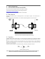
To our customers,
Old Company Name in Catalogs and Other Documents
On April 1st, 2010, NEC Electronics Corporation merged with Renesas Technology
Corporation, and Renesas Electronics Corporation took over all the business of both
companies. Therefore, although the old company name remains in this document, it is a valid
Renesas Electronics document. We appreciate your understanding.
Renesas Electronics website: http://www.renesas.com
April 1st, 2010
Renesas Electronics Corporation
Issued by: Renesas Electronics Corporation (http://www.renesas.com)
Send any inquiries to http://www.renesas.com/inquiry.
Notice
1.
2.
3.
4.
5.
6.
7.
All information included in this document is current as of the date this document is issued. Such information, however, is
subject to change without any prior notice. Before purchasing or using any Renesas Electronics products listed herein, please
confirm the latest product information with a Renesas Electronics sales office. Also, please pay regular and careful attention to
additional and different information to be disclosed by Renesas Electronics such as that disclosed through our website.
Renesas Electronics does not assume any liability for infringement of patents, copyrights, or other intellectual property rights
of third parties by or arising from the use of Renesas Electronics products or technical information described in this document.
No license, express, implied or otherwise, is granted hereby under any patents, copyrights or other intellectual property rights
of Renesas Electronics or others.
You should not alter, modify, copy, or otherwise misappropriate any Renesas Electronics product, whether in whole or in part.
Descriptions of circuits, software and other related information in this document are provided only to illustrate the operation of
semiconductor products and application examples. You are fully responsible for the incorporation of these circuits, software,
and information in the design of your equipment. Renesas Electronics assumes no responsibility for any losses incurred by
you or third parties arising from the use of these circuits, software, or information.
When exporting the products or technology described in this document, you should comply with the applicable export control
laws and regulations and follow the procedures required by such laws and regulations. You should not use Renesas
Electronics products or the technology described in this document for any purpose relating to military applications or use by
the military, including but not limited to the development of weapons of mass destruction. Renesas Electronics products and
technology may not be used for or incorporated into any products or systems whose manufacture, use, or sale is prohibited
under any applicable domestic or foreign laws or regulations.
Renesas Electronics has used reasonable care in preparing the information included in this document, but Renesas Electronics
does not warrant that such information is error free. Renesas Electronics assumes no liability whatsoever for any damages
incurred by you resulting from errors in or omissions from the information included herein.
Renesas Electronics products are classified according to the following three quality grades: “Standard”, “High Quality”, and
“Specific”. The recommended applications for each Renesas Electronics product depends on the product’s quality grade, as
indicated below. You must check the quality grade of each Renesas Electronics product before using it in a particular
application. You may not use any Renesas Electronics product for any application categorized as “Specific” without the prior
written consent of Renesas Electronics. Further, you may not use any Renesas Electronics product for any application for
which it is not intended without the prior written consent of Renesas Electronics. Renesas Electronics shall not be in any way
liable for any damages or losses incurred by you or third parties arising from the use of any Renesas Electronics product for an
application categorized as “Specific” or for which the product is not intended where you have failed to obtain the prior written
consent of Renesas Electronics. The quality grade of each Renesas Electronics product is “Standard” unless otherwise
expressly specified in a Renesas Electronics data sheets or data books, etc.
“Standard”:
8.
9.
10.
11.
12.
Computers; office equipment; communications equipment; test and measurement equipment; audio and visual
equipment; home electronic appliances; machine tools; personal electronic equipment; and industrial robots.
“High Quality”: Transportation equipment (automobiles, trains, ships, etc.); traffic control systems; anti-disaster systems; anticrime systems; safety equipment; and medical equipment not specifically designed for life support.
“Specific”:
Aircraft; aerospace equipment; submersible repeaters; nuclear reactor control systems; medical equipment or
systems for life support (e.g. artificial life support devices or systems), surgical implantations, or healthcare
intervention (e.g. excision, etc.), and any other applications or purposes that pose a direct threat to human life.
You should use the Renesas Electronics products described in this document within the range specified by Renesas Electronics,
especially with respect to the maximum rating, operating supply voltage range, movement power voltage range, heat radiation
characteristics, installation and other product characteristics. Renesas Electronics shall have no liability for malfunctions or
damages arising out of the use of Renesas Electronics products beyond such specified ranges.
Although Renesas Electronics endeavors to improve the quality and reliability of its products, semiconductor products have
specific characteristics such as the occurrence of failure at a certain rate and malfunctions under certain use conditions. Further,
Renesas Electronics products are not subject to radiation resistance design. Please be sure to implement safety measures to
guard them against the possibility of physical injury, and injury or damage caused by fire in the event of the failure of a
Renesas Electronics product, such as safety design for hardware and software including but not limited to redundancy, fire
control and malfunction prevention, appropriate treatment for aging degradation or any other appropriate measures. Because
the evaluation of microcomputer software alone is very difficult, please evaluate the safety of the final products or system
manufactured by you.
Please contact a Renesas Electronics sales office for details as to environmental matters such as the environmental
compatibility of each Renesas Electronics product. Please use Renesas Electronics products in compliance with all applicable
laws and regulations that regulate the inclusion or use of controlled substances, including without limitation, the EU RoHS
Directive. Renesas Electronics assumes no liability for damages or losses occurring as a result of your noncompliance with
applicable laws and regulations.
This document may not be reproduced or duplicated, in any form, in whole or in part, without prior written consent of Renesas
Electronics.
Please contact a Renesas Electronics sales office if you have any questions regarding the information contained in this
document or Renesas Electronics products, or if you have any other inquiries.
(Note 1) “Renesas Electronics” as used in this document means Renesas Electronics Corporation and also includes its majorityowned subsidiaries.
(Note 2) “Renesas Electronics product(s)” means any product developed or manufactured by or for Renesas Electronics.
To all our customers
Regarding the change of names mentioned in the document, such as Hitachi
Electric and Hitachi XX, to Renesas Technology Corp.
The semiconductor operations of Mitsubishi Electric and Hitachi were transferred to Renesas
Technology Corporation on April 1st 2003. These operations include microcomputer, logic, analog
and discrete devices, and memory chips other than DRAMs (flash memory, SRAMs etc.)
Accordingly, although Hitachi, Hitachi, Ltd., Hitachi Semiconductors, and other Hitachi brand
names are mentioned in the document, these names have in fact all been changed to Renesas
Technology Corp. Thank you for your understanding. Except for our corporate trademark, logo and
corporate statement, no changes whatsoever have been made to the contents of the document, and
these changes do not constitute any alteration to the contents of the document itself.
Renesas Technology Home Page: http://www.renesas.com
Renesas Technology Corp.
Customer Support Dept.
April 1, 2003
EDK2239
USER MANUAL
FOR H8S/2239
ON-CHIP FLASH MICROCONTROLLER
Preface
Cautions
1.
This document may be, wholly or partially, subject to change without notice.
2.
All rights reserved. No one is permitted to reproduce or duplicate, in any form, a part or this entire
document without Hitachi Micro Systems Europe Limited's written permission.
Trademarks
General
All brand or product names used in this manual are trademarks or registered trademarks of their respective
companies or organisations.
Specific
Microsoft, MS and MS-DOS are registered trademarks and Windows and Windows NT are
trademarks of Microsoft Corporation.
Document Information
Product Code:
D004183_11
Version:
1.0
Date:
20/11/2002
Copyright © Hitachi Micro Systems Europe Ltd. 1995-2002. All rights reserved.
Global:
http://www.hitachisemiconductor.com
Europe:
http://www.hmse.com
2
1.
TABLE OF CONTENTS
1.
TABLE OF CONTENTS ............................................................................................................................................. 3
2.
START-UP INSTRUCTIONS ....................................................................................................................................... 4
2.1. INSTALLING THE EVALUATION DEVELOPMENT KIT (EDK)........................................................................... 4
2.2. SERIAL CONNECTION ....................................................................................................................................... 4
2.3. POWER SUPPLY ................................................................................................................................................ 4
3.
EDK BOARD LAYOUT ............................................................................................................................................ 5
3.1. EDK BLOCK DIAGRAM....................................................................................................................................... 5
4.
EDK OPERATION ................................................................................................................................................... 6
4.1. USER INTERFACE.............................................................................................................................................. 6
4.2. SERIAL INTERFACE........................................................................................................................................... 6
4.3. SRAM................................................................................................................................................................... 7
4.4. MEMORY MAP .................................................................................................................................................... 8
4.5. SRAM ACCESS TIMING ..................................................................................................................................... 8
4.6. LEDS.................................................................................................................................................................... 8
5.
BOARD OPTIONS .................................................................................................................................................... 9
5.1. JUMPER LINKS................................................................................................................................................... 9
5.2. USER MODE SETTINGS – CJ5........................................................................................................................ 10
5.3. EDK OPTIONS – CJ4 ........................................................................................................................................ 10
5.4. SERIAL PORT SELECTION.............................................................................................................................. 11
5.5. FLASH PROGRAMMING HEADER .................................................................................................................. 11
5.6. BOOT CONTROL .............................................................................................................................................. 12
6.
MICROCONTROLLER HEADER CONNECTIONS ......................................................................................................... 13
6.1. HEADER J1 ....................................................................................................................................................... 13
6.2. HEADER J2 ....................................................................................................................................................... 14
7.
CODE DEVELOPMENT ........................................................................................................................................... 15
7.1. HMON ................................................................................................................................................................ 15
7.2. ADDITIONAL INFORMATION ........................................................................................................................... 17
3
2.
START-UP INSTRUCTIONS
2.1. INSTALLING THE EVALUATION DEVELOPMENT KIT (EDK)
Please refer to the quick start guide provided for initial installation of the EDK.
A copy of the quick start guide and other information relating to this EDK at:
http://www.hmse.com/products/edk/support/
Installing the EDK requires power and serial connection to a host computer.
2.2. SERIAL CONNECTION
The serial communications cable for connecting the EDK to a host computer is supplied. The serial cable has 1:1
connectivity.
Figure 2-1 shows how to connect the EDK to a PC or notebook computer equipped with a nine pin D connector.
HOST
PC
EDK
3
2
5
3
2
5
FIGURE 2-1: SERIAL CONNECTION TO PC/NOTEBOOK WITH DB-9 CONNECTOR (SUPPLIED)
2.3. POWER SUPPLY
The EDK hardware requires a power supply of +5V. Since total power consumption can vary widely due to external
connections, port states, and memory configuration, use a power supply capable of providing at least 500mA at +5V DC ±
5%.
The design is specified for evaluation of the microcontroller and so does not include circuitry for supply filtering/noise
reduction, under voltage protection, over current protection or reversed polarity protection. Caution should be used when
selecting and using a power supply.
The power connector on the EDK is a 2.5mm Barrel connector. The center pin is the positive connection.
FIGURE 2-2: POWER SUPPLY CONNECTION
Caution: Existing customers using E6000 products note that the polarity of this board is opposite to that for the
E6000. Use of the E6000 power supply with this board will damage both board and power supply.
4
3.
EDK BOARD LAYOUT
The diagram shows a general layout of the EDK board.
FLASH
Programming
Power
J1
Testpoints
XTAL
BOOT
Switch
OSC
BOOT LED
Power LED
User1 LED
User2 LED
9-Way
D-Type
5V
3V3
UVcc
GND
RESn
FW
NMIn
ULED1
ULED2
PSCK
PTXD
PRXD
RX232
DTXD
DRXD
NMI
Switch
RESET
Switch
MD4
HITACHI
Microprocessor
RXDISn
DCTS
DRTS
CJ5
SRAM
MD0
MD1
MD2
MD3
UPM
CSn
J2
CJ4
FIGURE 3-1: EDK BOARD LAYOUT
3.1. EDK BLOCK DIAGRAM
The diagram shows the connectivity of the components on the EDK board.
5V PSU
Reset
Boot
NMI
Switches
Control Logic
5V Supply
&
3V3 Regulator
EDK specific
SRAM
RS232
Programming
& Comms
HITACHI
Microprocessor
LEDs
User1 Power
&
&
User2 Boot
Header
Connectors
FIGURE 3-2: EDK BLOCK DIAGRAM
5
4.
EDK OPERATION
4.1. USER INTERFACE
The EDK provides three buttons for influencing the operation of the board. The purpose of each button is clearly marked next
to it. Refer to the board layout for positions (Section 3)
1.
Reset Switch
This button provides the microcontroller with a timed reset pulse of at least 250mS.
2.
Boot Switch
This button toggles the operating mode of the microcontroller. A complete description of this function is given in
section 5.6.
3.
NMI Switch
This button provides a de-bounced signal to the microcontroller for each operation of the button. There is no minimum or
maximum activation time for this button.
4.2. SERIAL INTERFACE
The serial interface on the EDK board has several functions. The serial port on the microcontroller directly supports three
wire serial interfaces. Options are provided on the board for the user to write handshaking routines using standard port pins.
Other board option links allow users to control the entry and exit from boot mode using the same handshaking signals. Refer
to section 5 for details on setting serial interface options.
4.2.1. CONNECTOR PIN DEFINITIONS
The EDK RS232 interface conforms to Data Communication Equipment (DCE) format allowing the use of 1-1 cables when
connected to Data Terminal Equipment (DTE) such as an IBM PC. The cable used to connect to the EDK will affect the
available board options. A fully wired cable can allow handshaking between the microcontroller and the host PC, subject to
setting the board options and the availability of suitable host software. Handshaking is not supported as standard on the
microcontroller so for normal use a minimal three-wire cable can be used. The minimum connections are unshaded in the
following table.
EDK DB9
Connector Pin
1
2
3
4
5
6
7
8
9
Signal
Host DB9
Connector Pin
No Connection
EDK Tx Host Rx
EDK Rx Host Tx
No Connection
Ground
No Connection
* EDK CTS Host RTS
* EDK RTS Host CTS
No Connection
1
2
3
4
5
6
7
8
9
TABLE 4-1: RS232 INTERFACE CONNECTIONS
* These are not connected on the EDK by default. See section 5.4 for more details.
5
4
9
3
8
2
7
1
6
FIGURE 4-1: EDK SERIAL PORT PIN NUMBERING
6
4.2.2. CRYSTAL CHOICE
The operating crystal frequency has been chosen to support the fastest operation with the fastest serial operating speeds.
The value of the crystal is 14.745MHz.
The following table shows the baud rates and Baud Rate Register (BRR) setting required for each communication rate using
the above default operating speed. It also confirms the resultant baud rate and the bit error rate that can be expected.
Baud Rate Register Settings for Serial Communication Rates
SMR
0
Setting:
Comm.
BRR
Actual
ERR
Baud
setting
Rate
(%)
110
invalid invalid invalid
300
invalid invalid invalid
1200 invalid invalid invalid
2400 191
2400
0.00
1
BRR
setting
Actual
Rate
2
ERR
(%)
BRR
setting
3
Actual
Rate
ERR
(%)
BRR
setting
Actual
Rate
ERR
(%)
invalid
invalid
invalid
invalid
invalid
invalid
64
110.77
0.70
invalid
invalid
invalid
95
300
0.00
23
300
0.00
95
1200
0.00
23
1200
0.00
5
1200
0.00
47
2400
0.00
11
2400
0.00
2
2400
0.00
4800
95
4800
0.00
23
4800
0.00
5
4800
0.00
1
3600
-25.00
9600
47
9600
0.00
11
9600
0.00
2
9600
0.00
invalid
Invalid
invalid
19200
23
19200
0.00
5
19200
0.00
1
14400
-25.00
invalid
Invalid
invalid
38400
11
38400
0.00
2
38400
0.00
invalid
invalid
invalid
invalid
invalid
invalid
57600
7
115200 3
230400* 1
57600
0.00
1
57600
0.00
invalid
invalid
invalid
invalid
invalid
invalid
115200
0.00
0
115200
0.00
invalid
invalid
invalid
invalid
invalid
invalid
230400
0.00
invalid
invalid
invalid
invalid
invalid
invalid
invalid
invalid
invalid
460800* 0
460800
0.00
invalid
invalid
invalid
invalid
invalid
invalid
invalid
invalid
invalid
TABLE 4-2 CRYSTAL FREQUENCIES FOR RS232 COMMUNICATION
* Note: The device used to convert the RS232 serial information to logic signals for the microcontroller is limited to
120kBaud. The rates above this level can only be utilised if the user provides direct logic level communications.
The user may replace the HC49/U surface mounted AT cut crystal with another of similar type within the operating frequency
of the microcontroller device. Please refer to the hardware manual for the microcontroller for the valid operating range.
Alternatively the user may fit an oscillator module – or provide an external clock source. When providing an oscillator module
or external source it is highly recommended that the load capacitors for the AT crystal are removed from the PCB. These are
physically placed within the PCB outline of the oscillator module for easy location and to ensure they are removed when
using this option.
When changing the crystal frequency the pre-loaded debugging monitor will not function. In this situation the user is
responsible for providing code to evaluate the device away from the default operating speed.
4.2.3. REMOVABLE COMPONENT INFORMATION.
This information is provided to allow the replacement of components removed from the board as described in section 4.2.2.
Component
Load Resistor (X2)
Load Resistor (X3)
Load capacitors (X2)
Load capacitors (X3)
Cct. Ref
R8
R7
C1,C2
C3,C4
Value
1MΩ
1MΩ
22pF
15pF
Rating
0805 1%
0805 1%
0603 10% 25V
0603 10% 25V
Manufacturer
Welwyn WCR Series
Welwyn WCR Series
AVX 0603 3 A 220 KAT
AVX 0603 3 A 150 KAT
TABLE 4-3: REMOVABLE COMPONENT INFORMATION
Care must be taken not to damage the tracking around these components. Only use soldering equipment designed for
surface mount assembly and rework.
4.3. SRAM
Provision has been made for a 4MBit SRAM device on the board, allowing 256kx16 operation.
Please refer to the schematic for details of the components to be fitted for external SRAM functionality.
SCI2, used as the default serial port for the EDK, shares the upper two address lines (A17 & A18). These may be isolated
from the SRAM by not fitting 0R links (R20 & R23), and pulling up the address lines on the SRAM using 4K7 resistors (R21 &
R22). This allows for a (64k x 16) configuration.
7
Alternatively the device may be programmed using SCI2, but configured to use the debug serial port (SCI0), as detailed in
section 5.4, for access to the full address range (256k x 16).
The SRAM, (when fitted), is connected to Chip Select 1 (CS1), which can address the range H200000 – H27FFFF. The
usable address range without modifying the board jumpers mentioned, is H’200000 – H’21FFFF.
4.4. MEMORY MAP
Table 4-4 illustrates the EDK memory map for mode 6.
Section Start
Section End
H’0000 0000
H’0005 FFFF
H’0006 0000
H’001F FFFF
H’0020 0000
H’0027 FFFF
H’0028 0000
H'00FF 6FFF
H'00FF 7000
H'00FF EFBF
H'00FF EFC0
H'FFFF F7FF
H'FFFF F800
H'FFFF FF3F
H'FFFF FF40
H'FFFF FF5F
H'FFFF FF60
H'FFFF FFBF
H'FFFF FFC0
H’FFFF FFFF
Section Allocation
On-Chip ROM
RESERVED
SRAM (A1-A18) Area 1 (controlled by CS1)
RESERVED
On-Chip RAM
RESERVED
Internal I/O Registers
RESERVED
Internal I/O Registers
On-Chip RAM
TABLE 4-4: MEMORY MAP (DEFAULT MODE 2)
4.5. SRAM ACCESS TIMING
External access timing is defined by several registers, allowing different types of devices to be addressed. The registers for
the selection of wait states and signal extensions are given below with recommended values for the EDK.
Register
ABWCR
ASTCR
WCRH
WCRL
PFCR
PFCR
Address
FFFED0
FFFED1
FFFED2
FFFED3
FFFDEB
FFFDEB
Recommended
Setting for EDK
H’FD
H’FF
H’FF
H’FF
H’09
H’0B
Function
Enables 16-bit access to area 1
3-State access
3-Wait state access
3-Wait state access
Enables A16 to A8 (used when SCI2.is used)
Enables A18 to A8 (used when SCI2.is not used)
TABLE 4-5: SRAM ACCESS CONTROL REGISTERS
Please refer to the hardware manual for the microcontroller for more information on these register settings.
4.6. LEDS
The EDK has four red LEDs. The function of each LED is clearly marked on the silk screen of the PCB. Please refer to the
board layout diagram for position information (Section 3).
When the board is connected to a power source the Power (PWR) led will illuminate. The Boot mode indication LED will
illuminate when the microcontroller has been placed into Boot mode. Please see section 2 for more details of this function.
There are two LEDs dedicated for user control these are marked USR1 and USR2. Each LED will illuminate when the port
pin is in a logical high state.
The user LEDs are connected to the following ports:
LED
Identifier
USR1
USR2
Port
Pin
P10
P11
Microcontroller
Pin
34
35
Pin Functions on Port Pin
P10/TIOCA0/DACK0n/A20
P11TIOCB/DACK1/A21
TABLE 4-6: LED PORT CONNECTIONS
8
5.
BOARD OPTIONS
The EDK has a number of configuration settings set by jumpers CJ4 (A, B, C, D) CJ5 (A, B, C, D) and zero-ohm links.
Common EDK functions can be set using the jumpers as described in sections 5.3 and 5.2. The additional zero-ohm links
provide additional features that may be required to interface with other systems.
All the Jumper link settings are three pin options. There are four sets of options on each header.
The headers are numbered from 1 to 12 with pin 1 marked on the PCB by an arrow pointing to the pin. The diagram below
shows the numbering of these jumper links and indicates jumpers fitted 1-2 for each three-pin jumper.
5.1. JUMPER LINKS
MD4
FLASH
Programming
5V
3V3
UVcc
GND
Power
1
BOOT
Switch
3
RXDISn
DCTS
DRTS
4
1 2 3
Jumper
C
1,2,3
7
5
1 2 3
Jumper
B
1,2,3
CJ5
9-Way
D-Type
XTAL
2
1 2
3
Jumper
A
1,2,3
BOOT LED
Power LED
User1 LED
User2 LED
OSC
RESn
FW
NMIn
ULED1
ULED2
PSCK
PTXD
PRXD
RX232
DTXD
DRXD
NMI
Switch
RESET
Switch
J1
HITACHI
Microprocessor
SRAM
MD0
MD1
MD2
MD3
UPM
6
CSn
J2
8
CJ4
9 10 11
12
1 2 3
Jumper
D
1,2,3
1 2
3
1 2 3
Jumper
A
1,2,3
4
5
6
1 2 3
Jumper
B
1,2,3
7
8
9 10 11
1 2 3
Jumper
C
1,2,3
12
1 2 3
Jumper
D
1,2,3
FIGURE 5-1: JUMPER CONFIGURATION
The following tables define each jumper and its settings.
9
5.2. USER MODE SETTINGS – CJ5
CJ5 is used to set the operating mode of the microcontroller.
These jumpers must be fitted at all times to ensure correct operation of the EDK.
Jumper
CJ 5-A
Default 2-3
CJ 5-B
Default 1-2
CJ 5-C
Default 2-3
CJ 5-D
Default 1-2
Function
Setting 1-2
Setting 2-3
User Mode Setting Bit 0
MD0 pulled High
MD0 pulled Low
User Mode Setting Bit 1
MD1 pulled High
MD1 pulled Low
User Mode Setting Bit 2
MD2 pulled High
MD2 pulled Low
User Mode Setting Bit 3
MD3 pulled High
MD3 pulled Low
TABLE 5-1: USER MODE: JUMPER SETTINGS (DEFAULT SETTINGS IN BOLD)
The default settings indicated in bold text place the microcontroller into Mode 6.
5.3.
EDK OPTIONS – CJ4
The EDK options provide access to commonly used features of the EDK range.
These jumpers must be fitted at all times to ensure correct operation of the EDK.
Jumper
Function
CJ 4-A
Default 2-3
Serial Receive
Source
CJ 4-B
Default 2-3
User
Programming
Mode
CJ 4-C
Default 2-3
CJ 4-D
Not Fitted
Chip select
Enable
Setting 1-2
Disables the RS232 receive signal
to enable the use of the Flash
Programming Header
Disables the Flash write hardware
protection.
The flash can be overwritten in
User Mode.
Connect CSn of the SRAM to PG3
of the H8S/2239
Setting 2-3
Enables the RS232 receive signal.
The Flash Programming Header*
must not be used in this state.
Enables the Flash write hardware
protection.
The flash cannot be overwritten in
User Mode.
Isolate and pull high, CSn of the
SRAM
Not Used
TABLE 5-2: BOARD OPTION: JUMPER SETTINGS (DEFAULT SETTINGS IN BOLD)
*See section 5.5
The following table lists the connections to each jumper pin.
Pin
1
2
3
4
5
6
7
8
9
10
11
12
Net Name
UVCC
RXDISn
No Connection
UVCC
UPM
No Connection
PG3
CSn
No Connection
No Connection
No Connection
No Connection
Description
Microcontroller Supply Voltage
Disable Flash Header functions. Pulled low. (Enables RX232)
No Connection
Microcontroller Supply Voltage
CPLD Controlled option to set Flash Write (FW). Pulled low.
No Connection
Port G3 of the H8S/2239 (CS1)
Chip select of the SRAM, and a 4K7 pull up.
No Connection
No Connection
No Connection
No Connection
10
5.4. SERIAL PORT SELECTION
The programming serial port is connected to the RS232 connector by default. This allows direct programming of the EDK
using the supplied software tools. A secondary serial port is available on the microcontroller and can be connected to the
RS232 connector by changing some board option links. The additional port option allows the user to write messages or
connect to other devices via the serial port while programming support is provided by the Flash programming header.
The following surface mount, zero-ohm link settings are fitted by default and connect the RS232 header to the programming
serial port of the microcontroller.
Zero-ohm
Link ID
CR20
CR23
CR19
CR22
Default
Fitted
Fitted
Not Fitted
Not Fitted
Function
Transmit data from EDK
Receive data to EDK
Alternate Transmit data from EDK
Alternate Receive data to EDK
Microcontroller
Port Pin
PA1
PA2
P30
P31
TABLE 5-3: OPTION LINKS – DEFAULT SETTINGS
To enable the use of this alternate port the user must change the settings to those in the following table.
Zero-ohm
Link ID
CR20
CR23
CR19
CR22
Default
Not Fitted
Not Fitted
Fitted
Fitted
Function
Transmit data from EDK
Receive data to EDK
Alternate Transmit data from EDK
Alternate Receive data to EDK
Microcontroller
Port Pin
PA1
PA2
P30
P31
TABLE 5-4: OPTION LINKS – ALTERNATE SERIAL PORT
The user may implement a handshaking protocol on the EDK. This is not supported with the software tools supplied. To
support this option two spare port pins have been allocated on the microcontroller. Using these port pins the CTS and RTS
lines of the host serial interface can be controlled.
The user may also control the operation of the board via the same handshaking lines. This is not supported with the software
tools supplied but may be written by the user. Using the CTS line the user may simulate pressing the boot button, see
section:5.6. This will cause the EDK to swap into and out of Boot mode on each low-level activation of CTS. Feedback of the
current mode is provided on the RTS line. A high level indicates boot mode and a low level indicates user mode.
The following settings are made by default, and ensure that there are no conflicts on unnecessary microcontroller pins.
Zero-ohm
Link ID
CR12
CR7
CR16
CR13
Default
Not Fitted
Not Fitted
Not Fitted
Not Fitted
Function
Mode State out from EDK
Change Mode request to EDK
Alternate RTS232 – Ready to send – from EDK
Alternate CTS232 – Clear to send – to EDK
Microcontroller
Port Pin
N/A (From CPLD*)
N/A (From CPLD*)
P15
P14
TABLE 5-5: OPTION LINKS – SERIAL PORT CONTROL
* See section 5.6
Note:
These setting pairs are exclusive:
If CR12 and CR7 are fitted; CR16 and CR13 must not be fitted.
If CR16 and CR13 are fitted; CR12 and CR7 must not be fitted.
5.5. FLASH PROGRAMMING HEADER
The Flash Programming header is used with the Hitachi Flash Debug Board (FDB). The FDB is a USB based programming
tool for control and programming of Hitachi microcontrollers, available separately from Hitachi. This header provides direct
access for the FDB to control the EDK microcontroller.
To utilise this header the user must make the following changes to the board configuration.
1.
Disable the RX232 signal from the RS232 transceiver.
Jumper link CJ4-A is provided for this purpose. Please refer to section5.3.
2.
Disable User Program Mode using jumper CJ4-B. Please refer to section5.3.
Caution: Do not operate the board with the user mode jumpers removed and the FDB disconnected, as the
microcontroller mode pins will float to an indeterminate state. This may damage the microcontroller device.
11
5.6. BOOT CONTROL
The method for placing the microcontroller device in to Boot mode for reprogramming has been incorporated into a complex
programmable logic device (CPLD). This is not necessary for most user designs but allows a measure of increased flexibility
for the EDK designs. Mode transitions including boot mode transitions only require the reset to be held active while the mode
settings are presented. On releasing reset the microcontroller will be in the required mode.
The logic design detects a power up event and provides a timed reset pulse to guarantee the reset of the device. At the end
of the rest pulse the processor will be placed in user mode and any code in the device will execute.
During user mode the NMI button can be pressed at any time. This will provide a single de-bounced NMI interrupt to the
device.
Pressing the boot button will cause the boot mode controller to reset the device and, during the reset period, present the
required mode settings to start the device in boot mode. At the end of the reset period the boot mode settings will have been
latched into the device, which will then be ready to accept a boot mode connection via the RS232 interface or the flash
programming header. Pressing the boot button during a normal reset will not cause the EDK to enter boot mode.
The boot mode settings are fixed at mode 2. The required mode settings are made using a tri-state capable buffer.
Note:
The boot control device is programmed to support all possible EDK products.
For this reason the reset pulse is over 500ms. Repetitive activation of either the Boot or Reset buttons will restart
the reset timer and extend the reset period. Pressing the boot button within the 500mS period of a reset will not
cause the board to enter boot mode.
5.6.1. CPLD CODE
The code is based upon a four state machine providing a guaranteed reset period, which can be extended by holding the
relevant control input in the active state. When released the timer will extend the reset for approximately 500mS.
The states are split into two functions, one for User mode and one for Boot mode. The first state of each is used to hold the
reset line active. When the timer expires then the second state is used to hold the device in the selected mode and wait for
an external control signal to either move back into the user reset state or into the boot reset state.
5.6.2. STATE DIAGRAM
Boot Mode Controller : Positive Logic
(CTS+BootSw) . /Res
Waiting
Boot
/Res . Boot
Res
Reset Timer
/Res
ResSw . /Res
Res
/Res
/Res . Reset
Clocked Transitions
using NE555
(All solid transition
lines)
Reset
(BootSW + ResSw + CTS)
. /Res
BootWaiting
Async
FIGURE 5-2: CPLD STATE DIAGRAM
12
6.
MICROCONTROLLER HEADER CONNECTIONS
The following table lists the connections to each or the headers on the board.
6.1. HEADER J1
J1
Pin
No
1
3
5
7
9
11
13
15
17
19
21
23
25
STBYn
RESn
CON_OSC2
MD0
CON_Vref
P41
P43
P45
P47
P97
P17
DRTS
P13
ULED2
35
28
29
STBY
RES
OSC2
MD0
Vref
P41/AN1
P43/AN3
P45/AN5
P47/AN7
P97/DA1
P17/TIOCB2/TCLKD
P15/TIOCB1/TCLKC
P13/TIOCD0/TCLKB/
A23
P11/TIOCB0/DACK1/
A21
PA3/A19/SCK2
Device
pin
61
59
57
55
53
51
49
47
45
43
41
39
37
PSCK
33
30
31
33
35
37
39
41
43
45
47
49
PA1/A17/TxD2
PB7/A15/TIOCB5
PB5/A13/TIOCB4
PB3/A11/TIOCD3
PB1/A9/TIOCB3
PC7/A7
PC5/A5
PC3/A3
PC1/A1
PC0/A0
PTXD
PB7
PB5
PB3
PB1
PC7
PC5
PC3
PC1
PC0
31
29
27
25
23
21
19
17
15
13
32
34
36
38
40
42
44
46
48
50
27
Function
EDK Symbol
Pin
No
2
4
6
8
10
12
14
16
18
20
22
24
26
Function
EDK Symbol
VCC
NMI
OSC1
MD1
AVCC
P40/AN0
P42/AN2
P44/AN4
P46/AN6
P96/DA0
AVSS
P16/TIOCA2/IRQ1
P14/TIOCA1/IRQ0
UVCC
NMIn
CON_OSC1
MD1
CON_AVCC
P40
P42
P44
P46
P96
CON_AVSS
P16
DCTS
Device
pin
62
60
58
56
54
52
50
48
46
44
42
40
38
P12/TIOCC0/TCLKA/A
22
P10/TIOCA0/DACK0/A
20
PA2/A18/RxD2
PA0/A16
PB6/A14/TIOCA5
PB4/A12/TIOCA4
PB2/A10/TIOCC3
PB0/A8/TIOCA3
PC6/A6
PC4/A4
PC2/A2
VSS
P12
36
ULED1
34
PRXD
PA0
PB6
PB4
PB2
PB0
PC6
PC4
PC2
Ground
32
30
28
26
24
22
20
18
16
14
13
6.2. HEADER J2
J2
Pin
No
1
3
5
7
9
11
13
15
17
19
21
23
25
27
29
31
33
35
37
39
41
43
45
47
49
Function
EDK Symbol
XTAL
EXTAL
MD2
PF6/AS
PF4/HWR
CON_XTAL
CON_EXTAL
MD2
PF6
PF4
Device
pin
63
65
67
69
71
PF2/WAIT
PF0/BREQ/IRQ2
P31/RxD0
P33/TxD1/SCL1
P35/SCK1/SCL0/IRQ
5
P77/TxD3
P75/TMO3/SCK3
P73/TMO1/TEND1/C
S7
P71/TMRI23/TMCI23
/DREQ1/CS5
PG0/IRQ6
PG2/CS2
PG4/CS0
PE1/D1
PE3/D3
PE5/D5
PE7/D7
D9/PD1
D11/PD3
D13/PD5
D15/PD7
PF2
PF0
DRxD
P33
P35
73
75
77
79
81
P77
P75
P73
Pin
No
2
4
6
8
10
Function
EDK Symbol
Ground
FW
PF7
PF5
PF3
12
14
16
18
20
VSS
FWE
PF7/ø
PF5/RD
PF3/LWR/IRQ3/ADTR
G
PF1/BACK/BUZZ
P30/TxD0
P32/SCK0/SDA1/IRQ4
P34/RxD1/SDA0
P36
Device
pin
64
66
68
70
72
PF1
DTxD
P32
P34
P36
74
76
78
80
82
83
85
87
22
24
26
P76/RxD3
P74/TMO2/MRES
P72/TMO0/TEND0/CS6
P76
P74
P72
84
86
88
P71
89
28
P70
90
PG0
PG2
PG4
PE1
PE3
PE5
PE7
PD1
PD3
PD5
PD7
91
93
95
97
99
1
3
5
7
9
11
30
32
34
36
38
40
42
44
46
48
50
P70/TMRI01/TMCI01/D
REQ0/CS4
PG1/CS3/IRQ7
PG3/CS1
PE0/D0
PE2/D2
PE4/D4
PE6/D6
D8/PD0
D10/PD2
D12/PD4
D14/PD6
CVCC
PG1
PG3
PE0
PE2
PE4
PE6
PD0
PD2
PD4
PD6
NC12
92
94
96
98
100
2
4
6
8
10
12
14
7.
CODE DEVELOPMENT
7.1. HMON
7.1.1. MODE SUPPORT
The HMON library is built to support Advanced Expanded Mode only. The Device supports Modes 6 and 7.
7.1.2. BREAKPOINT SUPPORT
The monitor utilises the PC Break Controller for code located in ROM, allowing a single breakpoint to be set in the code.
Code located in RAM may have multiple breakpoints limited only by the size of the On-Chip RAM.
7.1.2.1.CODE LOCATED IN FLASH / ROM
Double clicking in the breakpoint column in the code sets the breakpoint. Adding a further breakpoint elsewhere in the code
removes the previous one.
7.1.2.2.CODE LOCATED IN RAM
Double clicking in the breakpoint column in the code sets the breakpoint. Breakpoints will remain unless they are double
clicked to remove them.
7.1.3. HMON CODE SIZE
HMON is built along with the debug code. Certain elements of the HMON code must remain at a fixed location in memory.
The following table details the HMON components and their size and location in memory. For more information, refer to the
map file when building code.
Section
Description
Start Location
Size
(H’bytes)
RESET_VECTOR
HMON Reset Vector (Vector 0)
Required for Startup of HMON
Trap Vectors (Vector 8, 9, 10, 11)
Required by HMON to create Trap Breakpoints in RAM
HMON Break Controller (Vector 27)
Required by HMON to create Breakpoints in ROM
HMON Serial Port Vectors (Vector 88, 89, 90)
Used by HMON when EDK is configured to connect to the
default serial port.
HMON Code
HMON Constant Data
HMON Uninitialised data
FDT User Mode Kernel.
This is at a fixed location and must not be moved. Should the
kernel need to be moved it must be re-compiled.
FDT User Mode Kernel.
This is at a fixed location and must not be moved. Should the
kernel need to be moved it must be re-compiled.
Pointer used by HMON to point to the start of user code.
This is at a fixed location and must not be moved for the Reset
CPU, and Go Reset commands to function.
H’ 000000000
4
H’ 00000020
10
H’ 0000006C
4
H’ 00000160
C
H’ 00003000
H’ 000054CE
H’ 00FFB000
H’ 00001000
24CE
148
20F
11A
H’ 0005F600
80A
H’ 00002000
4
TRAP_VECTORS
HW_BREAK_VECTORS
SCI_VECTORS
PHMON
CHMON
BHMON
FDTInit
FDTUserModeMicroKernel
CUser_Vectors
15
7.1.4.
MEMORY MAP
H'00000000
Vectors
RESET Vector
TRAP Vectors
H'00001000
H'00001119
H'00002000
H'00002003
H'00003000
H'00005615
FDTInit
HW Break Vector
H'0000006C
H'0000006F
SCI Vectors
H'00000160
H'0000016B
CUser_Vectors
PHMON
CHMON
H'00000000
H'00000003
H'00000020
H'0000002F
On-Chip FLASH
ROM
H'0005F600
H'0005FE09
H'0005FFFF
FDTUserModeMicr
oKernel
H'00200000
SRAM
(when fitted)
H'0027FFFF
H'00FF7000
H'00FFB000
H'00FFB20E
H'00FFEDB0
H'00FFEFAF
H'00FFEFBF
H'00FFF800
H'00FFFF40
H'00FFFF60
On-Chip RAM
BHMON
Stack
Internal I/O
REGISTERS
Internal I/O
REGISTERS
H'00FFFFC0
On-Chip RAM
H'00FFFFFF
16
7.1.5.
BAUD RATE SETTING
HMON has initially set to connect at 115200Baud. Should the user wish to change this, the value for the BRR in
HMONserialconfiguser.c will need to be changed and the project re-built. Please refer to the HMON User Manual for further
information.
7.1.6.
INTERRUPT MASK SECTIONS
HMON has an interrupt priority of 6. The serial port has an interrupt priority of 7. Modules using interrupts should be set to
lower than this value (6 or below), so that serial communications and debugging capability is maintained.
7.2. ADDITIONAL INFORMATION
For details on how to use Hitachi Embedded Workshop (HEW), with HMON, `refer to the HEW manual available on the CD
or from the web site.
For information about the H8S/2239 series microcontrollers refer to the H8S/2239 Series Hardware Manual
For information about the H8S/2239 assembly language, refer to the H8S Series Programming Manual
Further information available for this product can be found on the HMSE web site at:
http://www.hmse.com/products/support.htm
General information on Hitachi Microcontrollers can be found at the following URLs.
Global:
www.hitachisemiconductor.com
Europe:
www.hmse.com
17