1
SIDSA
Chapter 3
Configurable Analog Block
FIPSOC
User’s Manual
SIDSA
Semiconductor Design Solutions
Configurable Analog Block (CAB)
1. Overview
The Field Programmable System On Chip (FIPSOC)
constitutes a new concept in system integration. It
provides the user with the possibility of integrating a
microprocessor core along with programmable digital
and analog cells within the same integrated circuit.
This chip can be considered as a large granularity
FPGA with a FPAA (Field Programmable Analog
Array) and a built-in microprocessor core that does not
only act as a general purpose processing element, but
also configures the programmable cells and their
interconnections. Therefore, there is a strong
interaction between hardware and software as long as
signal values and configuration data within the
programmable cells are accessible from microprocessor
programs.
This chapter describes the functionality of the
Configurable Analog Block (CAB), which is the basic
programmable analog tile to be used within FIPSOC
chips. It is a large granularity cell oriented to data
acquisition frontend applications. It supports four input
differential channels, and it is internally built using
fully balanced differential structures to provide a good
noise rejection. A flexible data acquisition block
provides four 8-bit conversion channels which can be
independently used as DACs (Digital to Analog
Converter) or ADCs (Analog to Digital Converter).
Two 8-bit channels can be combined to form a 9-bit
block, and the four of them can be used as a 10-bit
channel. Input signals can be converted after
amplification or from direct inputs, and the 10-bit ADC
supports a multiplexed mode to convert the four
channels with 10-bit resolution. The references for the
DACs (the ADCs make use of the DACs with a
successive approximation algorithm) can be set from
internal or external signals, the output signals coming
from the amplification channels, or more DAC outputs
themselves. This way, two 8-bit DACs can
dynamically set the references of a remaning 8-bit
DAC or ADC, and analog multiplications can be
performed.
2. Block Diagram an I/O Pins
A simplified block diagram of the CAB can be found
in fig. 2.1, and a detailed one is shown in fig. 2.2
Comparators
Gain
Block
Reference Block
Data
Conversion
Block
Output
Buffers
Fig 2.1: Simplified Block Diagram of the Configurable Analog Block (CAB)
Chapter 3. Configurable Analog Block (CAB)
2
SIDSA
Semiconductor Design Solutions
Fig 2.2: Detailed Block Diagram of the Configurable Analog Block (CAB)
Four major blocks are shown in fig. 2.1: The Gain
Block (see section 3: Gain Block), the Data Conversion
Block (see section 4: Data Conversion Block), the
Comparators Block (see section 5: Comparators Block)
and the Reference Block (see section 6: Reference
Block). However, these three blocks are completely
interrelated in a very flexible manner: The references
for the amplifying stages and the AD/DA converters
are provided by the reference block, while you can set
references using DACs or outputs of some amplifying
stages. This way, the DACs can set the common mode
references of the amplifying sections, and the analog
signals coming thru the amplification channels can set
as well the references of the DAC/ADCs.
2.1 External I/O signals (bonding pads)
The signals marked with crossed boxes in the detailed
block diagram (fig. 2.2) are external I/O pins tied to
bonding pads. All of them are described hereby:
In1P, In1N, In4P, In4N: These are the global
differential inputs for amplification channels #1 and
#4. They are always internally buffered before entering
the programmable amplifying stages.
In2P, In2N, Out2P, Out2N, In3P, In3N, Out3P,
Out3N: These are the global differential inputs and
outputs for amplification channels #2 and #3. Two
operating modes are supported: In the normal mode,
these channels behave like channels #1 and #4 (Input
signals are internally buffered before entering the first
programmable amplfiying stage); in the direct mode,
the user has direct access to the first fully balanced
differential amplifier of each channel. In both cases,
Out2P and Out2N (Out3P and Out3N for channel #3)
Chapter 3. Configurable Analog Block (CAB)
are the direct outputs of the first fully balanced
differential amplifier of the the channel (see section 3:
Gain Block).
Ref8, Ref0: They are the inputs to the voltage divider
of the reference block from which the normal
references are generated from. Note that an internal
16K ±30% resistor is placed between these two pins
(see section 6: Reference Block).
RefX: This is high impedance extra reference input.
O3P, O4P: These are the positive outputs of channels
3 and 4 for external use.
OD1-4: They are the buffered outputs of the DACs.
Note that they can be used even when the converters
are working in an ADC mode to monitor the succesive
approximation algorithm.
2.2 Internal I/O ports
The signals marked with arrows in the block diagram
(fig. 2.2) are in internal I/O ports connected to the
digital macro cells (DMCs), that is, the programmable
logic. These signals have their counterparts mapped as
registers for microprocessor access. All of them are
described hereby:
PLOutComp1-4: These are the digital outputs of the
four comparators (see section 5: Comparators Block).
PLconv1-4: A high level on these signals activates the
conversion process in the corresponding ADC (see
section 4: Data Conversion Block).
PLdone1-4: These signals go high when the related
conversion ends.
3
SIDSA
Semiconductor Design Solutions
PLout(7:0): This is the output data bus from the ADCs
(see section 4: Data Conversion Block).
PloutExt(1:0): These two signals are an extension
from the output data bus when a 9- or 10-bits ADCs are
configured.
PLselout(2:0): These are the selection signals for
reading the output registers of the DACs (see section 4:
Data Conversion Block).
PLinA(7:0), PLinB(7:0), PLinC(7:0), PLinD(7:0):
These are the (digital) input buses for the
corresponding DACs (see section 4: Data Conversion
Block).
2.3 Internal Signals
We describe here the internal signals coming from
reference voltage divider and from the output of
amplification channels. These signals are used
references for the different blocks and as inputs for
data conversion block.
the
the
as
the
O1P to O4P, O1N to O4N: These signals are the
outputs of the last gain stage of each amplification
channel (see section 3: Gain Block).
Ref0 to Ref8: These are the outputs of the voltage
divider of the reference block (see Fig. 2.2). This
resistor ladder provides nine evenly spaced voltages
from Ref8 to Ref0 (see section 6: Reference Block).
sig1 to sig4: These are the outputs of the Gain Block.
An analog multiplexer selects the signal to route to
these signals from the outputs of each amplification
channel (O1P to O4P, O1N to O4N) and the direct
inputs In2N, In2P, In3N and In3P.
opref1, opref2: These are the reference inputs for the
common mode voltage at the output of the gain stages
of channels #1 and #2 (opref1) and #3 and #4 (opref2).
cmpref1, cmpref2: These are the reference inputs for
comparators #1 and #2 (cmpref1) and #3 and #4
(cmpref2).
dacref1 to dacref5: These are the five reference input
voltages for the DACs (see section 4: Data Conversion
Block).
2.4 µP Control Registers
The µP can control both the configuration and
operation of the analog cells from the digital interface
to them. The control registers for controlling the digital
side of the mixed signal cells are listed underneath:
OutComp(3:0): This read-only register maps the
output of the four comparators (see section 5:
Comparators Block).
Chapter 3. Configurable Analog Block (CAB)
mPconv(3:0): This nibble is used to trigger
conversions. A logical one writen to each bit starts the
conversion on the corresponding ADC channel (see
section 4: Data Conversion Block).
mPdone(3:0): This nibble represents the status of each
ADC. Each bit goes high when a conversion ends in
the corresponding channel. This action is masked by
adc_enINT(3:0) (see section 4: Data Conversion
Block).
dat1(7:0)-dat4(7:0): These read/write registers are
used to store converted data from each channel in the
ADC modes, and to place digital data to be converted
in the DAC modes (see section 4: Data Conversion
Block).
dat5(7:0)-dat8(7:0): These read-only registers store
the converted data from channels Ch#3 and Ch#4 when
the 4-input multiplexed 10-bits ADC mode is selected
(see section 4: Data Conversion Block).
2.5 Configuration Registers
The µP controls the configuration of all programmable
features of the analog cells. The configuration
information of the whole CAB is stored in a 64-byte
static RAM block mapped onto the microprocessor
memory space. The configuration data is listed below,
and a comprehensive table with the addresses and
organization is given afterwards.
Note: This 64-byte memory bank is relocated on the FIPSOC
absolute address map depending on the operating mode.
gs1(3:0) - gs12(3:0): These nibbles control the gain
factor of amplifying sections 1 thru 12 in linear steps
from 0 to 15 (see section 3: Gain Block).
off1(7:0) - off12(7:0): These bytes control the offset of
the amplifying sections 1 thru 12 (see section 3: Gain
Block).
CMRR1(3:0) - CMRR12(3:0): These nibbles control
the CMRR compensation circuitry of amplifying
sections 1 thru 12 (see section 3: Gain Block).
opref1(3:0), opref2(3:0): These nibbles select the
output common mode reference for the amplifying
channels (the three gain stages of a channel share the
same reference) #1 and #2 (opref1) and #3 and #4
(opref2) (see section 3: Gain Block and section 6:
Reference Block).
dacref1(3:0) - dacref5(3:0): These nibbles select the
reference for the DAC/ADC block (see section 4: Data
Conversion Block and section 6: Reference Block).
cmpref1(3:0), cmpref2(3:0): These nibbles select the
reference for comparators #1 and #2 (cmpref1) and #3
and #4 (cmpref2) (see section 5: Comparators Block
and section 6: Reference Block).
4
SIDSA
ONdacbuf(3:0): This nibble enables output buffers for
DAC channels when the corresponding bit is set to one
(see section 4: Data Conversion Block).
ONcmp: This bit enables when clear to zero the
comparators block.
ONdacref(4:0): This 5-bit word enables when the
corresponding bit is set to one the reference buffers for
the DAC/ADC channels (see section 4: Data
Conversion Block).
inpsig(7:0): This byte selects the active signals from
the gain block to be converted and compared (see
section 3: Gain Block).
adc_group(3:0): This nibble configures the different
modes of operation of the ADC/DAC (see section 4:
Data Conversion Block).
Semiconductor Design Solutions
the differential inputs of channel #x, and OxP and OxN
are its outputs. Each channel has a differential buffered
input (each input is buffered with a single-ended
operational amplifier) and three subsequent
programmable gain stages. Each gain stage is fully
balanced: This means that the output differential
voltage equals the input differential voltage multiplied
by a (programmable) constant factor regardless of the
input common mode voltage, as depicted in fig. 3.2.
Note: In block diagrams of figures 2.2 and 3.1, each gain stage is
represented as a triangle with two inputs on the left (positive and
negative), one input on the right (the reference voltage for the output
common mode) and two outputs on the right (positive and negative).
This symbol does not represent here a fully balanced differential
operational amplifier like in fig. 3.3, but a complete programmable
gain stage with a finite input impedance.
adc_select(3:0): This nibble startups when the
corresponding bit is set to one the ADC configuration
of each channel (see section 4: Data Conversion
Block).
Vcommon
VInP
Voltage
adc_cconv(3:0): This nibble enables the continuous
conversion mode in channels configured as ADCs (see
section 4: Data Conversion Block).
VInN
VOutN
Vref
adc_source(3:0): This nibble selects the control source
from either the Programmable Logic or the µP for each
channel.
VOutP
Time
adc_enINT(3:0): This is the interrupt mask for the
four ADC channels. Interrupts are enabled when set to
one (see section 4: Data Conversion Block).
ONamp(3:0): This nibble enables, when the
corresponding bit is set to one, each amplification
channel, including all bias circuits and fully balanced
operational amplifiers (see section 3: Gain Block).
Dir2N, Dinr3N: These bits select when reset to zero
the direct access mode for the first fully balanced
operational amplifiers of channels #2 and #3 (see
section 3: Gain Block).
Cal(3:0): When set to one, each bit of this nibble
enters the corresponding channel into calibration mode,
which connects both plus and minus input terminals of
each input stage to the internal ref4 signal (see section
3: Gain Block).
3. Gain Block
A diagram of the Gain Block can be observed in fig.
3.1. It consists of twelve differential gain stages
organized in four channels. Inputs InxP and InxN are
Chapter 3. Configurable Analog Block (CAB)
Fig. 3.2: Waveform Display of a Fully Balanced Differential Gain
Stage. Vcommon is the common mode voltage at the input.
The output common mode voltage is directly set using
a reference input. Each two channels share the same
reference signal (opref1 for channels #1 and #2,
opref2 for channels #3 and #4) which is obtained from
the reference block (the reference signals are selected
by configuration registers opref1(3:0) and opref2(3:0);
see section 6: Reference Block). Channels #2 and #3
provide the differential outputs of the first gain stage
on pins Out2P and Out2N (channel #2) and Out3P and
Out3N (channel #3). It is also provided a direct access
mode to the first fully balanced differential operational
amplifiers of channels #2 and #3.
In general, output signals OxP and OxN at the end of
the amplification channels are internally used for
conversion, comparison and references. Only the
positive output signals from channels three and four
O3P and O4P are connected to output bonding pads
with the same name.
5
SIDSA
Semiconductor Design Solutions
Fig. 3.1: Gain Block
The amplification channels of the Gain Block have a
power down feature which can be used to cut the
power supply for the selected cells. The three gain
stages of each channel share the same power down bit.
To set a complete channel in the power down mode,
the corresponding bit in configuration register
ONamp(3:0) must be reset to zero (ONamp(0)
corresponds to channel #1, ONamp(3) corresponds to
channel #4).
Note: When a gain stage is set to the power down mode, all bias
currents and input resistors are disconnected. Appropriate settling
times must be allowed upon subsequent power up.
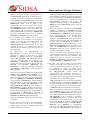
3.1 Gain Stage
Fig. 3.3 qualitatively shows the structure of a gain
stage.
Note: In figures 3.3 and 3.4 the triangle represents a fully balanced
differential operational amplifier with infinte input impedance. It
does not symbolize a complete gain stage like in figures 2.2 and 3.1.
Different gains are obtained by modulating the input
resistance Rin . A gain select nibble gs(3:0) is used to
program the gain of the stage in linear steps from 0 to
15. The offset of the differential output signal can be
configured by injecting a differential current regulated
by an offset select byte off(7:0) in increasing discrete
values from -128 to 127. Each step correspond
approximately to a 1.5mV of differential voltage at the
output. Four extra bits CMRR(3:0) are used to
intendedly asymmetrize the two branches of the
differential system by slightly modulating only one of
the feedback branches with a small exra resistor RCMRR,
thus giving an extra degree of freedom to adjust the
CMRR, which greatly depends on the exact matching
of the two branches. The CMRR function should have
a minimum within the interval 0 to 15 of the
CMRR(3:0) nibble.
Note: It is not guaranteed the monotonicity nor a good linearity of
the offset control, so this feature should not be used to build an 8bit digital to analog converter (concrete specifications will be given
in the next version of this manual).
3.2 Direct Access to Operational Amplifiers
Fig. 3.3: Internal Structure of a Gain Stage
Chapter 3. Configurable Analog Block (CAB)
As depicted in fig. 3.3, each gain stage is based on a
fully balanced differential operational amplifier. It is
possible to directly access these cells by selecting the
direct mode, only available for channels #2 and #3. To
select the direct mode, bits Dir2N (for channel #2) or
Dir3N (for channel #3) must be reset to zero (they
have to be set to one for normal operation). In this
mode, pins In2P, In2N, Out2P and Out2N are the
direct inputs and outputs of a fully balanced differential
operational amplifier whose output is also connected to
the two remaining gain stages of channel #2 (In3P,
In3N, Out3P and Out3N can be used the same way in
channel #3). Fig. 3.4 presents channels #3 and #4 in the
6
SIDSA
Semiconductor Design Solutions
direct access mode. Note that subsequent gain stages
(AMP#6 in channel #2 and AMP#7 in channel #3) do
load the operational amplifiers.
PLinA-D(7:0)
PLout(7:0)
4 x Channels
Regs.
cmp
Bus mP.
SAR
DAC
Int Gen.
Fig. 3.4: Channels #2 and #3 configured for direct access
(Dir2N=Dir3N=0)
IN1- 4
Figure 4.1. Diagram of the conversion block
4.1 Architecture description
3.3 Output Signal Selection
The Gain Block has four main outputs labeled sig1 to
sig4. These signals are directly driven to the input of
the ADCs and comparators. Only these four signals can
be converted or compared.
The outputs of the Gain Block are directly multiplexed
from the internal output signals coming from the final
gain stages, and from the external input signals of
channels #2 and #3. Configuration register inpsig(7:0)
selects the signals to route to the output. The following
four tables show the possible combinations.
References: The four DACs are powered by five
buffered voltage references. Each pair of references
gives the positive and negative reference voltages for
each converter so reference voltages are shared by each
two adjacent DACs as depicted in Figure 4.2. The
activity of each buffer is controlled by the µP setting
the corresponding bit of Ondacref(4:0). The dinamic
range of these reference buffers is rail to rail (between
VSS+0.2V and VDD-0.2V).
Ondacref(0)
Vref1
inpsig(1)
0
0
1
1
Inpsig(0)
0
1
0
1
Sig1
In2N
In2P
O1N
O1P
Table 3.1: sig1 selection
inpsig(3)
0
0
1
1
inpsig(2)
0
1
0
1
sig2
In2N
In2P
O2N
O2P
Table 3.2: sig2 selection
Ondacref(1)
CH #1
DAC1
CH #2
DAC2
CH #3
DAC3
CH #4
DAC4
Vref2
Ondacref(2)
Vref3
inpsig(5)
0
0
1
1
inpsig(4)
0
1
0
1
sig3
In3N
In3P
O3N
O3P
Table 3.3: sig3 selection
Inpsig(7)
0
0
1
1
inpsig(6)
0
1
0
1
sig4
In3N
In3P
O4N
O4P
Ondacref(3)
Vref4
Table 3.4: sig4 selection
Ondacref(4)
4. Data Conversion Block
The Data Conversion Block consists of four Digital to
Analog converters (DACs) used for general purpose
analog output, four Successive Approximation
Registers (SARs) which can be used together with the
DACs to convert analog external data into digital
words, and a bank of 8 to 10-bit registers where digital
information is stored. A diagram of the conversion
block is shown in Figure 4.1
Chapter 3. Configurable Analog Block (CAB)
Vref5
Figure 4.2. Reference structure for DACs
If a DAC is not to be used, noise and consumption can
be reduced by turning it off (i.e., disabling both
references).
In grouped modes (9/10-bits converters) where several
DACs are cascaded, common references must be
7
SIDSA
Semiconductor Design Solutions
disabled so as to obtain linear conversion (see the
Application Notes section for non-linear conversion).
LS
Digital to Analog Converters: Each one of the four
digital to analog converters consists of a 256 resistor
divider connected between two buffered references,
and a 8-bit decoder which selects the corresponding
output voltage. Two 8-bit cascaded DACs can be used
as a 9-bit DAC using a final analog multiplexer
governed by the MSB of the 9-bit word, and ditto for
using two 9-bit DACs to form a 10-bit block.
Vref
− Vref
P
N
256
Table 4.1: Conversion table for a single 8-bit DAC
The positive and negative reference voltages
assignment depends on DACs grouping configuration
(described later in section 4.2). According to the labels
used for signals in Figure 4.2., references for each
DAC are depicted on Table 4.2.
In 9-bit modes, two 8-bit DACs are fed with the same
word (the eight less significant bits). The highest one is
used to select their outputs as final voltage. In the 10bit DAC mode, the four DACs share the same word
(the eight less signinficant bits) while the two most
significant bits select the output from the four DACs.
The digital word to convert can come either from the
programmable logic, from the µP through the In/Out
registers or from the output of the SARs (closing the
A/D conversion loop). The selection of this multiplexer
is controlled by the AD/DA configuration of each
channel and the nibble adc_source(3:0).
Successive Approximation Registers: The data
conversion
block
contains
four
successive
approximation registers (SARs) composed of 8 bits
used to obtain analog to digital conversions in
association with the internal DACs (Figure 4.4). There
is one independent SAR per channel, which receives
the successive comparisons results and programs the
associated DAC to the next approximation.
The conversion table for a single 8-bit DAC is listed
below in table 4.1:
Word
0x00
0x01
0x02
.....
0xFE
0xFF
=
where V
Output
VrefN
VrefN + VLS
VrefN + 2 VLS
VrefP - 2 VLS
VrefP - VLS
Table 4.2. Reference assignments
DAC #1
adc_group
VrefP
DAC #2
VrefN
VrefP
DAC #3
VrefN
DAC #4
VrefP
VrefN
VrefP
VrefN
Vref3
Vref4
Vref5
Vref4
00XX
Vref1
Vref2
Vref3
Vref2
0101
Vref1
Vref2
Vref3=Vref1
Vref2
Vref3=Vref1 Vref4=Vref2 Vref5=Vref1 Vref4=Vref2
0110
Vref1
Vref2
Vref3=Vref1
Vref2
Vref3=Vref1
Vref4
Vref5
Vref4
0111
Vref1
Vref2
Vref3=Vref1
Vref2
Vref3=Vref1
Vref4
Vref5=Vref3
Vref4
DAC #1234 → VrefP = Vref1, VrefN = Vref5. Vref2 = off, Vref3 = off, Vref4 = off.
1000
1001
Vref1
Vref2
Vref3
Vref2
1010
DAC #12 → VrefP = Vref1, VrefN = Vref3. Vref2 = off.
1011
DAC #12 → VrefP = Vref1, VrefN = Vref3. Vref2 = off.
Vref4
Vref3
Vref4
Vref5
DAC #34 → VrefP = Vref5, VrefN = Vref3. Vref4 = off.
DAC #1234 → VrefP = Vref1, VrefN = Vref5. Vref2 = off, Vref3 = off, Vref4 = off.
1100
DAC #12 → VrefP = Vref1, VrefN = Vref3. Vref2 = off.
1101
1110
Vref1
Vref2
Vref3=Vref1
Vref2
DAC #12 → VrefP = Vref1, VrefN = Vref3. Vref2 = off.
1111
Notes :
DAC #34 → VrefP = Vref3, VrefN = Vref5. Vref4 = off.
Vref4
Vref3
Vref4
Vref5=Vref3
DAC #34 → VrefP = Vref3, VrefN = Vref5. Vref4 = off.
DAC #34 → VrefP=Vref5=Vref1,VrefN=Vref3. Vref4=off.
a) 9/10-bit DACs are referred to as group of the number of the channels used
b) `off´ represents that buffer must be disabled to obtain a constant VLS (see Applications Notes).
c)
V
LS
=
Vref
− Vref
Vref − Vref
P
N
P
N
in 9-bits DACs ; and, V
=
in 10-bit DAC
512
LS
1024
Chapter 3. Configurable Analog Block (CAB)
8
SIDSA
Channels configured as DACs convert the digital word
stored in the corresponding 8-bit register when
controlled by the µP. Channels used as ADCs, set up
their results when the conversion ends. The converted
data can be read in two ways:
• operating to Plselout(2:0) to obtain data through
Plout(7:0) to the programmable logic, or
• addressing the control registers mapped as memory
locations from the µP.
cmp
SAR
Regs.
DAC
IN
Figure 4.3. Successive approximation ADC loop
The beginning of the conversion can be independently
controlled for each channel. The process is depicted
below in table 4.3.
Cycle
1
2
3
4
5
6
7
8
9
10*
result of comparison
A
B
C
D
E
F
G
H
I
-
Semiconductor Design Solutions
Approximation
0111 1111
A011 1111
AB01 1111
ABC0 1111
ABCD 0111
ABCD E011
ABCD EF01
ABCD EFG0
ABCD EFGH
ABCD EFGH
* in continuous conversion mode, this cycle will begin a new
conversion, linking with cycle 1.
Table 4.3: Conversion sequence
When the conversion block is programmed with 9- or
10-bit ADC channels, the corresponding SARs form
groups (SAR#1 & SAR#2 and/or SAR#3 & SAR#4 to
obtain 9-bit ADCs or all of them to obtain a 10-bit
converter); when this occurs, the grouped SARs work
one or two cycles phased, respectively. At the end of
each conversion , SARs send their results to the In/Out
Registers and enable the interrupt generation block. On
continuous conversion modes that would start another
conversion.
During the conversion cycles the conversion command
for each chhanel could be independently issued either
from the programmable logic or the µP. This would
provoke a failure in the running conversion and the
following one. This would be critical in continuous
conversion modes because the error would be
propagated and could lead to unexpected results.
In/Out Registers Block: It consists of four 8-bit and
two 10-bit registers used to store the input or output
digital data from the data conversion block. The 10-bit
registers have read-only access and they are used to
store data in 4-multiplexed channels ADCs
configuration.
Chapter 3. Configurable Analog Block (CAB)
If the conversion block groups any channels to create a
9/10-bit converter, two registers will be needed. In
µP-controlled converters more significant bits must be
written first (see Table 4.4).
PLselout(3:0)
000 (dat1*)
001 (dat2*)
010 (dat3*)
011 (dat4*)
100 (dat5*)
101 (dat6*)
110 (dat7*)
111 (dat*8)
data
Ch#1 (7:0)
Ch#2 (7:0)
Ch#3 (7:0)
Ch#4 (7:0)
-
9-bit ch.+
Ch#A (7:0)
Ch#A (8:1)
Ch#B (7:0)
Ch#B (8:1)
-
10-bit ch +
Ch#A (7:0)
Ch#A (9:2)
Ch#B (7:0) **
Ch#B (9:2) **
Ch#C (7:0) **
Ch#C (9:2) **
Ch#D (7:0) **
Ch#D (9:2) **
* µP control registers (see section 2.4) when µP controlled
** only available in 4-mux channel 10-bit converter
+
PLoutExt(1:0) gives the 2 least significant bits of the channel
selected
(for
example,
if
PLselout(3:0)=’b011,
PLout=Ch#B(9:2) and PLoutExt(1:0)=Ch#B(1:0)).
Table 4.4: Conversion outputs
Interrupt Generation Block: This block provides the
end of conversion signals when at least one channel is
configured as ADC. It has independent protocols for
the µP and the Programmable Logic. Both protocols
work simultaneously (it allows different control for the
start and end of conversion).
When a channel reaches the end of the conversion, this
block acts as follows :
• a pulse is sent through the corresponding bit of
PLdone1-4,
• If the corresponding bit is not masked by
adc_enINT(3:0), an interrupt is sent to the µP
(signal ADC_int) and the conversion status in the
nibble mPdone(3:0) is updated. Both adc_INT and
mPdone(3:0) are reset when the µP reads the
nibble.
In 9/10-bit conversion modes only the corresponding
bit of the first channel grouped is used.
4.2 Configuration
The configuration of this block is controlled from the
µP. To program the conversion block, the µP must
access to the 64 bit memory and write the information
in the corresponding addresses (see Section 7).
Different configurations are listed below in table 4.5:
9
SIDSA
adc_group(3:0)
00XX
0100
0101
0110
0111
1000
1001
1010
1011
1100
1101
1110
1111
Ch. #1
Ch. #2
Ch. #3
Ch. #4
8-bit
8-bit
8-bit
8-bit
1 channel of 8-bits and 4x sampling rates
8-bit
8-bit
1 ch. of 8-bit and 2x
1 ch. of 8-bit and 2x
8-bit
8-bit
1 ch. of 8-bit and 2x
1 ch. of 8-bit and 2x
1 channel of 10 bits
8-bit
8-bit
1 channel of 9 bits
1 channel of 9 bits
8-bit
8-bit
1 channel of 9 bits
1 channel of 9 bits
4-multiplexed channels 10-bit
1 ch. of 8-bit and 2x
1 channel of 9 bits
1 channel of 9 bits
1 ch. of 8-bit and 2x
1 channel of 9-bit and 2x sampling rate
Table 4.5: Operating modes and their configuration data
Configurations with double and four times sampling
rates are only supported for ADC modes, working as
independent DACs otherwise.
adc_select(3:0): A high level in the corresponding bit
sets the channel as an ADC (otherwise as a DAC).
adc_cconv(3:0): A high level in the corresponding bit
sets the channel to work in a continuous conversion
mode (otherwise in a single conversion mode).
adc_source(3:0): A high level in the corresponding bit
indicates that the channel works under the
Programmable Logic control (under the µP otherwise)
Ondacref(4:0): These bits enable the corresponding
reference buffers (see picture 4.2) for the 8-bit DACs.
The combination of these nibbles and bits allows the
converter block to operate with many different
configurations (see Applications Notes at the end of the
section).
4.3. Operating Modes
Semiconductor Design Solutions
If the corresponding bit in adc_source(3:0) is set to
one (i.e. adc_source(0) and adc_source(2) for
Channels Ch#1 & Ch#2 and Ch#3 & Ch#4,
respectively), the digital word to be converted
comes from the Programmable Logic on signals
{PLinB(7),PLinA(7:0)} (for channel Ch#1 &
Ch#2) or on signals {PLinD(7),PLinC(7:0)} (for
channel Ch#3 Ch#4).
If adc_source(0) is reset to zero, the digital word to
be converted by the 9-bit DAC of Ch#1 & Ch#2,
can be set from the µP by writing the MSB of the 9bit word on dat2(7:0) and the LSB of the 9-bit
word on dat1(7:0) (dat2(7:0) is internally latched
and must be written first). Ondacref(1) must be
reset to zero to ensure linear conversion.
If adc_source(2) is reset to zero, the digital word to
be converted by the 9-bit DAC of Ch#3 & Ch#4,
can be set from the µP by writing the MSB of the 9bit word on dat4(7:0) and the LSB of the 9-bit
word on dat3(7:0) (dat4(7:0) is internally latched
and must be written first). Ondacref(3) must be
reset to zero to ensure linear conversion.
The Output of channel Ch#1 (and channel Ch#3)
will be utilized as the output of the converter.
10-bit DACs. Channels Ch#1 & CH#2 & Ch#3 &
CH#4 can be joined together to construct a 10-bit
converter. If adc_source(0) is set to one, the digital
word to be converted comes from the
programmable
logic
on
signals
{PLinB(7:6),PLinA(7:0)}. If adc_source(0) is
reset to zero, the digital word to be converted by the
10-bit DAC can be set from the µP by writing the
MSB of the 10-bit word on dat2(7:0) and the LSB
of the 10-bit word on dat1(7:0) (dat2(7:0) must be
written first). Ondacref(4:0) must be loaded with
10001 5-bit word to obtain a linear conversion.
The digital word conversion is obtained through
channel Ch#1.
The operating modes can be divided according to the
number of bits and the nature (DAC or ADC) of the
conversion:
Any combination of channels is allowed (i.e. it can be
configured a 9-bit DAC with channel Ch#3 & Ch#4, a
8-bit DAC on channel Ch#2 and turn off channel #1)
- DAC modes
- ADC modes
8-bit DACs. Each channel can work independently as
an 8-bit DAC. If the corresponding bit in
adc_source(3:0) is set to one, the digital word to be
converted comes from the programmable logic on
signals PLinA(7:0) (for channel #1) thru
PLinD(7:0) (for channel #4). If the corresponding
bit in adc_source(3:0) is reset to zero, the digital
word to be converted can be set from the µP by
writing on the corresponding dat1(7:0) (for channel
#1) thru dat4(7:0) (for channel #4) register.
Any DAC can take part of an ADC´s loop. So any
configuration described before, can be utilized here
(for example, in a four 8-bit DACs configuration, two
of them might be used as ADC)
9-bit DACs. Channels Ch#1 & Ch#2 and/or channels
Ch#3 & Ch#4 can be grouped to form a 9-bit DAC.
Chapter 3. Configurable Analog Block (CAB)
8-bit (regular) ADC. Each 8-bit channel can be used as
an ADC. If the corresponding bit in
adc_source(3:0) is set to one, the start command is
obtained by applying a high level to the
corresponding signal PLconv1 thru PLconv4 from
the programmable logic. If the corresponding bit in
adc_source(3:0) is reset to zero, the conversion
10
SIDSA
starts by writing an 1 on the corresponding bit of
the mPconv(3:0) register from the microprocessor.
When the conversion is finished, the corresponding
signal PLdone1 thru PLdone4 sends a pulse one
clock cycle wide, and the corresponding bit in the
mPdone(3:0) nibble goes to high. If the
corresponding bit in the interrupt mask register
adc_enINT(3:0) is set, an interrupt is generated.
The mPdone(3:0) nibble is reset when read by the
microprocessor. The converted data can be read
either on PLout(7:0) by operating to Plselout(2:0)
from the programmable logic, or can be read on
dat1(7:0) thru dat4(7:0) register from the µP.
8-bit fast-sampling ADC. Channels Ch#1 & Ch#2,
Ch#3 & Ch#4, and Ch#1-Ch#4 can be grouped
together to convert the same analog input with
phased clock samplings, by writing on the
adc_group(3:0) register from the µP. If only two
channels are joint, a 2x sampling rate will be
obtained; the four channels group will provide a 4x
conversion rates.
In
2x-converters,
if
adc_source(0)
or
adc_source(2) is set to one, the start command is
obtained by applying a high level to signal
PLconv1 or PLconv3 from the programmable
logic. If adc_source(0) or adc_source(2) is reset to
zero, the conversion starts by writing an 1 on
mPconv(0) or mPconv(2) of the mPconv(3:0)
register from the microprocessor. Notice that only
PLconv1 and PLconv3 (mPconv(0) and
mPconv(2)) are used; in 4x sampling rate channel,
only PLconv1 or mPconv(0) is used (selected by
adc_source(0)).
When the conversion is finished, the corresponding
PLdone signal (PLdone1 and PLdone3 on 2x
channels or PLdone1 on 4xADC channel) sends a
pulse one clock cycle wide, and the corresponding
bit in the mPdone(3:0) (mPdone(0), mPdone(2)
on 2x channels or mPdone(0) on 4xADC channel)
and nibble goes high. If the corresponding bit in the
interrupt mask register adc_enINT(3:0) is set
(adc_enINT(0), adc_enINT(2) on 2x channels or
adc_enINT(0) on 4xADC channel), an interrupt is
generated. The mPdone(3:0) nibble is reset when
read by the microprocessor. The converted data can
be read either on PLout(7:0) by operating to
Plselout(2:0) from the programmable logic, or on
dat1(7:0) thru dat4(7:0) register from the µP.
Input of channel Ch#1 (and Ch#3) is utilized for the
conversion.
9-bit ADC. 9-bit converters work with both channels
SARs. The result is stored in the corresponding
In/Out registers. The input of channel Ch#1 (and
Ch#3) is used for the conversion.
Chapter 3. Configurable Analog Block (CAB)
Semiconductor Design Solutions
If adc_source(0) or adc_source(2) is set to one, the
start command is obtained by applying a high level
to the corresponding signal PLconv2 and PLconv4
from the programmable logic. If those bits of the
adc_source(3:0) register are reset to zero, the
conversion starts by writing an 1 on mPconv(1) or
mPconv(3) of the mPconv(3:0) register from the
microprocessor
When the conversion is finished, signal PLdone1
(channels Ch#1&Ch#2) or PLdone3 (channels
CH#3&Ch#4) sends a pulse one clock cycle wide,
and mPdone(0) and mPdone(2) nibble goes high.
If the corresponding bit in the interrupt mask
register adc_enINT(3:0) is set, an interrupt is
generated. The mPdone(3:0) nibble is reset when
read by the microprocessor. The converted data can
be read either on PLout(7:0) by operating to
Plselout(2:0) from the programmable logic, or on
dat1(7:0) thru dat4(7:0) register from the µP (see
Table 4.4). PLoutExt(1:0) is an extension of bus
PLout(7:0) where the 2 least significant bits of
each data converted are available.
The two 9-bit ADCs can also be used to obtain a 9bit fast-sampling ADC with 2x sampling rates. The
input of Ch#1 is used for the conversion. This
configuration starts its conversion by writing on
PLdone2 (or mPconv(1)). When the conversion is
finished, PLdone1 (or mPdone(0)) is used.
10-bit ADC. The 10-bit converter uses the In/Out
registers of channels Ch#1 and Ch#2 to store its
results (as described in section 4.1). The ADC can
be configured to obtain the analog signal
multiplexing the four channels inputs by writing on
the
adc_group(3:0)
register
form
the
microprocessor. This architecture provides a 4multiplexed channels 10-bit ADC. The conversion
ends when the four data information are obtained
and stored in their corresponding registers.
If adc_source(0) is set to one, the start command is
obtained by applying a high level to PLconv2 from
the programmable logic. If adc_source(0) is reset
to zero, the conversion starts by writing an ‘b0001
on mPconv(3:0) register from the microprocessor.
When the conversion is finished, the corresponding
signal PLdone1 sends a pulse one clock cycle
wide, and bit0 of mPdone(3:0) nibble goes high. If
the corresponding bit in the interrupt mask register
(adc_enINT(0)) is set, an interrupt is generated.
The mPdone(3:0) nibble is reset when read by the
microprocessor. The converted data can be read
either on PLout(7:0) by operating to PLselout(2:0)
from the programmable logic, or on dat1(7:0) thru
dat2(7:0) (up to dat8(7:0) in 4-multiplexed
channels 10-bit ADC mode) registers from the µP
(see Table 4.4). PLoutExt(1:0) is an extension of
11
SIDSA
bus PLout(7:0) where the 2 least significant bits of
each data converted are available.
ADC channels can also be programmed to make a
continuous conversion, setting to one the
corresponding bit of adc_cconv(3:0). In this
configuration, ADCs start a new conversion one cycle
after the end of the previous conversion.
Any DAC, ADC or AD/DA combination described or
deduced from these descriptions can be managed from
either the Programmable Logic or the µP, but only
configured by the µP writing to the corresponding
memory registers.
5. Comparators Block
As shown in the block diagram of fig. 2.2, four
comparators are available. Each two comparators share
a reference signal which is the threshold voltage to
which the input signal is to be compared. Reference
signal cmpref1 is the threshold input for comparators
#1 and #2, while cmpref2 serves comparators #3 and
#4 (the reference signals are selected by configuration
registers cmpref1(3:0) and cmpref2(3:0); see section
6: Reference Block).
The input signals for the comparators are the
multiplexed outputs of the gain block, namely sig1 to
sig4. Comparator #N compares signal sigN and is
intended to work after amplification channel #N. For
each comparator, the digital output yields one if the
input signal is bigger than the selected reference, and
zero otherwise.
6. Reference Block
This block comprises the resistor divider and the
reference selection multiplexer depicted in fig. 2.2.
Nine internal references are generated from reference
pins Ref8 and Ref0 and a 8-resistor voltage divider
opref2(3)
0
0
0
0
0
0
0
0
1
1
1
1
1
1
1
1
opref2(2)
0
0
0
0
1
1
1
1
0
0
0
0
1
1
1
1
opref2(1)
0
0
1
1
0
0
1
1
0
0
1
1
0
0
1
1
opref1(0)
0
1
0
1
0
1
0
1
0
1
0
1
0
1
0
1
opref2
OD1
OD2
OD3
OD4
O1P
O2P
RefX
Ref0
Ref1
Ref2
Ref3
Ref4
Ref5
Ref6
Ref7
Ref8
Table 6.2: Reference Selection for opref2
Chapter 3. Configurable Analog Block (CAB)
Semiconductor Design Solutions
(see fig. 2.2). The value of each of those resistors is 2
KΩ ±30%, and the matching is up to 0.1%. Reference
voltages are evenly spaced between Ref0 and Ref8.
The input impedance seen between pins Ref8 and
Ren0 is therefore 16 KΩ ±30%. RefX is used as an
extra reference pin with high (infinite) input
impedance.
The reference selection multiplexer chooses the
different reference voltages of the circuit among the
internal reference nodes and several internal input and
output signals, all of them depicted in fig 2.2.
Configuration registers opref1(3:0) and opref2(3:0)
select the actual signal to route to reference signals
opref1 and opref2. Registers cmpref1(3:0) and
cmpref2(3:0) determine the references for the
comparator cmpref1 and cmpref2. Registers
dacref1(3:0) through dacref5(3:0) select the reference
signals for the DACs of the data conversion block.
The following nine tables show the possible
combinations. All of the signals mentioned in the last
column of each table can be looked up in fig. 2.2.
opref1(3)
0
0
0
0
0
0
0
0
1
1
1
1
1
1
1
1
opref1(2)
0
0
0
0
1
1
1
1
0
0
0
0
1
1
1
1
opref1(1)
0
0
1
1
0
0
1
1
0
0
1
1
0
0
1
1
opref1(0)
0
1
0
1
0
1
0
1
0
1
0
1
0
1
0
1
opref1
OD1
OD2
OD3
OD4
O3P
O4P
RefX
Ref0
Ref1
Ref2
Ref3
Ref4
Ref5
Ref6
Ref7
Ref8
Table 6.1: Reference Selection for opref1
cmpref1(3)
0
0
0
0
0
0
0
0
1
1
1
1
1
1
1
1
cmpref1(2) cmpref1(1) cmpref1(0) cmpref1
0
0
0
OD1
0
0
1
OD2
0
1
0
OD3
0
1
1
OD4
1
0
0
O3P
1
0
1
O4P
1
1
0
RefX
1
1
1
Ref0
0
0
0
Ref1
0
0
1
Ref2
0
1
0
Ref3
0
1
1
Ref4
1
0
0
Ref5
1
0
1
Ref6
1
1
0
Ref7
1
1
1
Ref8
Table 6.3: Reference Selection for cmpref1
12
SIDSA
cmpref2(3)
0
0
0
0
0
0
0
0
1
1
1
1
1
1
1
1
cmpref2(2) cmpref2(1) cmpref2(0) cmpref2
0
0
0
OD1
0
0
1
OD2
0
1
0
OD3
0
1
1
OD4
1
0
0
O1P
1
0
1
O2P
1
1
0
RefX
1
1
1
Ref0
0
0
0
Ref1
0
0
1
Ref2
0
1
0
Ref3
0
1
1
Ref4
1
0
0
Ref5
1
0
1
Ref6
1
1
0
Ref7
1
1
1
Ref8
Table 6.4: Reference Selection for cmpref2
dacref2(3) dacref2(2) dacref2(1) dacref2(0)
0
0
0
0
0
0
0
1
0
0
1
0
0
0
1
1
0
1
0
0
0
1
0
1
0
1
1
0
0
1
1
1
1
0
0
0
1
0
0
1
1
0
1
0
1
0
1
1
1
1
0
0
1
1
0
1
1
1
1
0
1
1
1
1
dacref2
OD3
OD4
O3N
O3P
O4N
O4P
RefX
Ref0
Ref1
Ref2
Ref3
Ref4
Ref5
Ref6
Ref7
Ref8
Table 6.6: Reference Selection for dacref2
dacref4(3) dacref4(2) dacref4(1) dacref4(0)
0
0
0
0
0
0
0
1
0
0
1
0
0
0
1
1
0
1
0
0
0
1
0
1
0
1
1
0
0
1
1
1
1
0
0
0
1
0
0
1
1
0
1
0
1
0
1
1
1
1
0
0
1
1
0
1
1
1
1
0
1
1
1
1
Semiconductor Design Solutions
dacref1(3) dacref1(2) dacref1(1) dacref1(0)
0
0
0
0
0
0
0
1
0
0
1
0
0
0
1
1
0
1
0
0
0
1
0
1
0
1
1
0
0
1
1
1
1
0
0
0
1
0
0
1
1
0
1
0
1
0
1
1
1
1
0
0
1
1
0
1
1
1
1
0
1
1
1
1
dacref1
OD3
OD4
O3N
O3P
O4N
O4P
RefX
Ref0
Ref1
Ref2
Ref3
Ref4
Ref5
Ref6
Ref7
Ref8
Table 6.5: Reference Selection for dacref1
dacref3(3) dacref3(2) dacref3(1) dacref3(0)
0
0
0
0
0
0
0
1
0
0
1
0
0
0
1
1
0
1
0
0
0
1
0
1
0
1
1
0
0
1
1
1
1
0
0
0
1
0
0
1
1
0
1
0
1
0
1
1
1
1
0
0
1
1
0
1
1
1
1
0
1
1
1
1
dacref3
OD1
OD4
O1N
O1P
O4N
O4P
RefX
Ref0
Ref1
Ref2
Ref3
Ref4
Ref5
Ref6
Ref7
Ref8
Table 6.7: Reference Selection for dacref3
dacref4
OD1
OD2
O1N
O1P
O2N
O2P
RefX
Ref0
Ref1
Ref2
Ref3
Ref4
Ref5
Ref6
Ref7
Ref8
Table 6.8: Reference Selection for dacref4
Chapter 3. Configurable Analog Block (CAB)
dacref5(3) dacref5(2) dacref5(1) dacref5(0)
0
0
0
0
0
0
0
1
0
0
1
0
0
0
1
1
0
1
0
0
0
1
0
1
0
1
1
0
0
1
1
1
1
0
0
0
1
0
0
1
1
0
1
0
1
0
1
1
1
1
0
0
1
1
0
1
1
1
1
0
1
1
1
1
dacref5
OD1
OD2
O1N
O1P
O2N
O2P
RefX
Ref0
Ref1
Ref2
Ref3
Ref4
Ref5
Ref6
Ref7
Ref8
Table 6.9: Reference Selection for dacref5
13
SIDSA
Semiconductor Design Solutions
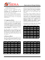
7. Configuration Data
In the following table, the word NU stands for not used. The memory locations marked with NU are physically
implemented but they have no significance for the configuration of the CAB. They can be used for general purpose data
storage.
Relative
Address
$00
$01
$02
$03
$04
$05
$06
$07
$08
$09
$0A
$0B
$0C
$0D
$0E
$0F
$10
$11
$12
$13
$14
$15
$16
$17
$18
$19
$1A
$1B
$1C
$1D
$1E
$1F
$20
$21
$22
$23
$24
$25
$26 - $3F
Bit
Nr
7
6
5
4
3
2
1
0
off1(7:0)
off2(7:0)
off3(7:0)
off4(7:0)
CMRR1(3:0)
CMRR2(3:0)
CMRR3(3:0)
CMRR4(3:0)
gs1(3:0)
gs2(3:0)
gs3(3:0)
gs4(3:0)
off5(7:0)
off6(7:0)
off7(7:0)
off8(7:0)
CMRR5(3:0)
CMRR6(3:0)
CMRR7(3:0)
CMRR8(3:0)
gs5(3:0)
gs6(3:0)
gs7(3:0)
gs8(3:0)
off9(7:0)
off10(7:0)
off11(7:0)
off12(7:0)
OCcmp
CMRR9(3:0)
CMRR10(3:0)
CMRR11(3:0)
CMRR12(3:0)
cmpref2(3:0)
opref2(3:0)
dacref5(3:0)
dacref3(3:0)
dacref1(3:0)
NU
NU
gs9(3:0)
gs10(3:0)
gs11(3:0)
gs12(3:0)
cmpref1(3:0)
opref1(3:0)
dacref4(3:0)
dacref2(3:0)
ONdacbuf(3:0)
ONdacref(4:0)
inpsig(7:0)
UN
adc_cconv(3:0)
adc_group(3:0)
NU
acd_source(3:0)
adc_select(3:0)
adc_enINT(3:0)
UN
Dir3N
Dir2N
NU
NU
NU
ONamp(3:0)
cal(3:0)
UN
Table 7.1: Configuration Memory
Chapter 3. Configurable Analog Block (CAB)
14
SIDSA
Semiconductor Design Solutions
8. Specifications
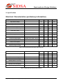
Electrical Characteristics (preliminary information)
Parameter
Test Conditions
Input Offset Voltage
Min
Typ
Max
Units
-2
0
2
mV
Open Loop Gain
100
dB
Unity gain bandwidth
2.6
MHz
Phase Margin
65
deg
Common Mode Input Range
VSS+0.2
CMRR (Differential output vs common
mode at the input)
DC / 1KHz
Output Source/Sink Current
VDD-0.2
V
85
dB
8
mA
Settling Time
0.85 to/from 1.85
1.2
µs
Slew Rate
rise/fall, load = 2KΩ , 100 pF
0.5
V/ µs
Overshoot (large signal)
rise/fall, load = 2KΩ , 100 pF
5
%
Startup Time
CL=50pF/50KΩ
5
µs
180
µA
Current Consumption
10
µW
3.3
3.6
V
Typ
Max
Units
-128
127
steps
-250
250
mV
Gain Factor Range
0
15
CMRR Correction Range
-8
CMRR (Without correction)
60
Standby Power Dissipation
Operating Supply Voltage
2.5
Table 8.1: Differential Operational Amplifier Preliminary Data
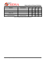
Parameter
Test Conditions
Offset Correction Range
Current Consumption
Min
Linear Zone
0
dB
µA
500
Standby Power Dissipation
Operating Supply Voltage
7
2.5
3.3
10
µW
3.6
V
Table 8.2: Differential Gain Section Preliminary Data
Chapter 3. Configurable Analog Block (CAB)
15
SIDSA
Parameter
Semiconductor Design Solutions
Test Conditions
Min
Resolution
Integral Non-linearity
Rail to Rail
Reference Voltage Range
Typ
Max
Units
8
Bit
0.5
LSB
VSS+0.2
VDD-0.2
V
Settling Time
200
ns
Startup Time
20
µs
Current Consumption
VRH=VDD, VRL=VSS
0.8
mA
Table 8.3: 8-bit Digital to Analog Converter Preliminary Data
Chapter 3. Configurable Analog Block (CAB)
16