1
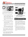
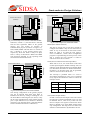
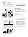
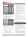
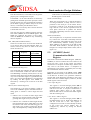
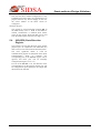
SIDSA
Chapter 8
Serial Communication Interface
FIPSOC
User’s Manual
SIDSA
Semiconductor Design Solutions
Serial Communication Interface
1. Overview
The Field Programmable System On Chip (FIPSOC)
constitutes a new concept in system integration. It
provides the user with the possibility of integrating a
microprocessor core along with programmable digital
and analog cells within the same integrated circuit.
This chip can be considered as a large granularity
FPGA with a FPAA (Field Programmable Analog
Array) and a built-in microprocessor core that does not
only act as a general purpose processing element, but
also configures the programmable cells and their
interconnections. Therefore, there is a strong
interaction between hardware and software as long as
signal values and configuration data within the
programmable
cells
are
accessible
from
microprocessor programs.
This chapter describes the Serial Communication
Block integrated on the FIPSOC system. It supports
two serial communication interfaces: a 2-wire protocol
and an SPI interface.
The 2-wire interface supports multi-devices serial data
communication using two lines. The 2-wire subblock
can be configured as either a master device or a slave
device. The block is identify by an address which can
be set via software.
The SPI interface is a synchronous interface which
allows several devices to be interconnected. Two wires
are required for data to obtain full duplex transfer
communication. A third line is used for clocking
purposes. The SPI subsystem supports different
communication rates and can be configured to be both
master or slave.
The Serial Communication Block would be
programmed by the software. However, it also supports
on-reset configuration (hardware configuration) in
order to provide more flexibility to the FIPSOC boot
procedure.
2. 2-Wire Serial Interface
This bus interface supports serial data transmission
using two lines between the devices connected to it.
The two wires are used to one for data (serial data –
SDA) and one for the clock signal (serial clock –SCL).
Multiple devices can be connected to the bus and can
operate as either a transmitter or receiver.
The transfer on the bus is initiated and controlled by a
master device that generates the clock signal; the other
devices, which send or receive data, are known as
slaves. Each device hanging in the bus is recognized by
an address. Any master-device must first identify the
desired slave by sending its address through the 2-wire
bus and configure it as either a transmitter or receiver
(read or write operations, respectively).
The 2-wire interface is multi-master. That is, more than
one device are capable of controlling the serial clock of
the bus.
2.1.
Bit Transfer
The transmission is controlled by the serial clock
(SCL). The SCL line is used to control each data bit
transferred. The data on the SDA line must be stable
during the high level of the SCL line. Level of the SDA
line can only change while the clock pulse on SCL is
low. Data changed during SCL high periods will
indicate a start or stop command (see figure 2.1).
bus free
bus busy
bus free
SCK
SDA
start condition
data valid
change of data
allowed
stop condition
Fig. 2.1: Bit transfer on the 2-wire interface
• Bus free: Both SDA and SCL are bi-directional
lines, connected to a positive supply via a pull-up
resistor (see figure 2.2). When the bus is free, no
transfer between any devices is in progress and
both lines stay high. All SDA and SCL outputs of
any devices connected to the bus must be opendrain (or open-collector) driven.
Note: 2-wire serial interface is not available in
device 8x12 of the FIPSOC family.
Chapter 8. Serial Communication Interface
2
SIDSA
Semiconductor Design Solutions
(see figure 2.1). After the stop condition, the bus is
considered to be free, and a high level must be set
in both SDA and SCL lines.
VDD
SCL (serial clock)
SDA (serial data)
SCL in
SCL in
SCL out SDA in
SCL outSDA in
SDA out
• Acknowledgement: All address and data words are
serially transmitted through the SDA line in 8-bit
words, most significant bit first. Each byte
transmitted is followed by an acknowledge bit set
by the receiver. The receiver must pull-down the
SDA line during the 9th clock cycle to acknowledge
that it has received each word. During this cycle,
the transmitter has to release the SDA line to
receive the confirmation from the receiver.
SDA out
Fig. 2.2: Connection of devices to the 2-wire bus
bus free
• Start Condition: A high-to-low transition in SDA
line with SCL high is a start condition (see figure
2.1). Only the master device may generate this
situation. The bus is considered to be busy after a
start condition. A start command always precedes
any command in the bus.
bus busy
SCL out by
transmitter
1
2
8
9
SDA out by
transmitter
not acknowledge
SDA out by
receiver
• Stop Condition: A low-to-high transition in SDA
while SCL is high is interpreted as a stop condition
acknowledge
start condition
clock pulse for acknowledge
Fig. 2.3: Acknowledge of receiver on the 2-wire bus
Bus busy
start condition
SCL
address word
1
1st data word
2
8
9
....... last data word
1
8
stop condition
9
read
SDA
MSB
write
address field
operation field
acknowledge cycles
Fig. 2.4: Data transfer on the 2-wire interface
2.2.
Data Transfer
After a start condition, the master device must send a
slave address. This first word has two purposes: firstly,
it is used to identify the slave device in the bus;
secondly, it is used to establish the transfer direction of
the communication (that is, configure the slave device
as receiver or transmitter). The first word is seven bits
long (address field) followed by an eight bit (operation
field) which is the R/W command select bit. A read
operation is initiated if this bit is high; otherwise, a
write operation is initiated (see figure 2.4).
The slave addressed must pull-down the ninth bit as
mentioned before (see figure 2.3). If the master device
do not detect a zero in the ninth clock cycle, no device
has been addressed. The master must then re-try to start
a communication or release the 2-wire bus. The first
action would be done by sending a different address
after a new start condition. The second one will be
done by producing a stop condition.
Chapter 8. Serial Communication Interface
The number of bytes that can be transmitted between
the start and the stop condition is unrestricted. Data
transfer is always finished by an stop command (see
figure 2.4). In other words, several start commands are
allowed without releasing the bus. Various
combinations of read/write format are possible in the
same transmission session. These formats are described
below (and shown in figure 2.5):
• Master transmitter: The master device transmits
data to the slave receiver. The transfer direction is
not changed, and the acknowledge bit is always set
by the slave. This format is used in write
operations.
• Master receiver: The master device reads data
from the slave after the first byte transmitted. The
transfer direction changes after the first byte (that
is, the address word transmission has master→ slave
direction while any other word is slave→ master
transmitted). The acknowledge bit is always set by
the receiver. Due to this fact only the first
3
SIDSA
Semiconductor Design Solutions
acknowledge bit is set by the slave (receiver
behavior)
• Combined format: It is used to change the
direction of a transfer or change the slave selected
without releasing the 2-wire bus. During a change
of direction, the Start Condition and the Slave
address are both repeated, but with the operation bit
reversed
Data transferred (n bytes + Ack)
S
Slave address
RW
A
Data
A
A/A
Data
P
Master-transmitter addresses a slave receiver. Transfer direction is not changed
Data transferred (n bytes + Ack)
1
S
Slave address
RW
A
Data
A
Data
A
P
(read)
S Slave address RW A
Direction and Ack.
depends on RW bits
Data A/A Sr Slave address RW A
Data transferred
(n bytes + Ack)
Data A/A P
Combined format
From master to slave
A
Acknowledge (SDA low)
From slave to master
A
Not acknowledge (SDA high)
S
Start Condition
P
Stop Condition
Sr
Repeated Start Condition
Fig. 2.5: Possible Data Transfer Formats
2.3.
Data out = 1, slave-receiver behavior
SCL
Data out device 1
losing arbitration
Data out device 2
SDA
Fig. 2.6: Arbitration procedure on the 2-wire interface
In other words, re-starting is not needed after the
multi-master conflict is arbitrated. If a master that
loses the arbitration can also behave as a slave, it is
possible that the master device would like to
establish a communication with it. In this case, the
losing master must change to its slave receiver
mode in order to acknowledge the addressing call
from the winning master.
• Clock Synchronization
A master reads a slave inmediately after the first byte
Data transferred
(n bytes + Ack)
start condition
Master devices generate the serial clock signal in
the SCL line. Since the 2-wire lines are pull-up
lines, any devices in the bus can alter the SCL
signal by obliging a low level in the line. Slow
slave-devices may use this characteristic to hold the
low period of the serial clock, leaving the master
device in a high wait-state. When all the devices
release the SCL line, the low-to-high transition will
occur and the master device will continue its
function (see figure 2.7).
Different slow operations can be handled thank to
this bus specification (pull-up resistor), such as
interrupt requesting on microcontrollers, data and
acknowledgement preparations, long-time needed
to store information and so on.
Arbitration
Special situations will appear when more than one
device try to initiate a data transfer at the same time or
devices with different speed responses are connected to
the bus. The first situation, called multi-master conflict,
requires an arbitration procedure; the second one,
requires a clock signal synchronization method.
• Multi-master arbitration
If two or more masters try to put information onto
the bus, the first device to produce a ‘one’ when the
other produces a ‘zero’ will lose the arbitration.
Note that bits transferred by the devices until that
moment are equal in both transmissions, so no
corrupted information is sent.
start condition
wait state
Master device clock
Slave device clock
SCL
SDA
starting high
period
starting low
period
Fig. 2.7: Clock synchronization procedure on the 2-wire interface
3. SPI Serial Interface
This bus interface is a synchronous interface which
allows several devices to be interconnected. Separate
wires are needed for data and clock. Two wires are
required for data to obtain full duplex transfer
communication. A third line is used for clocking
purposes.
The transfer on the bus is controlled by the master
device that generates the clock signal. A fourth signal
Chapter 8. Serial Communication Interface
4
SIDSA
Semiconductor Design Solutions
is used to recognize any device connected to the bus
(slave select signal).
generated. When the master device transmit data, the
slave device responds by sending data to the master.
This implies full duplex communication with both data
out and data in synchronized with the same serial
clock. A read operation is realized by sending a word
through the MOSI line (that is, generating the clock
signal in the SCK line).
The transmission between the master device and the
slave device selected is realized using two
unidirectional lines. A read operation is always
accompanied with a write operation (talk about
receiver and transmitter devices has no sense in this
interface).
3.1.
3.3.
Signal Description
The whole SPI system (master device, bus and slave
device) works like a system consisting of two shift
registers interconnected. The byte transmitted from the
master shift register is replaced by the byte received
from the slave. On the other side, the byte received
from the master in the slave shift register replaces the
previous word, which is sent to the master device via
the MISO line (see figure 3.1).
The four basic SPI signals are MISO, MOSI, SCK and
SS. They can be described as follows (as shown in
figure 3.1):
• Master in, Slave out (MISO): this signal is
configured as an input in a master device and as an
output in a slave device. It is one of the two lines
that transfers serial data in one direction. When
multiple slave devices are connected to the SPI bus,
this output must be placed in the high-impedance
state if the slave is not selected.
The SPI devices are double buffered on read, but not
on write. Thus, if a write is performed during data
transfer stored data will be erased, and both transmitted
and received data would be corrupted. In order to save
the data received, every eight cycles of the SCK the
shift register is copied to the buffer register.
• Master out, Slave in (MOSI): The MOSI line is
configured as an output in a master device and as
an input in a slave device. It is one of the two lines
that transfer data in one direction.
3.4.
• Serial Clock (SCK): The serial clock is used to
synchronize data movement both in and out of the
device through its MISO and MOSI lines. The
master device generates this signal, so it is
configured as an output in a master device and as
an input in a slave device.
A byte transmission is begun when the master device
writes on the shift register. This operation starts an
internal counter which generates eight cycles in the
SCK line.
Four possible timing relationships may be chosen for
the transmission depending on the synchronization
edge and level of the clock. Both master and slave
devices must operate with the same synchronization for
a right transmission. A bit transfer is made by placing
data on the MOSI and MISO lines a half-cycle before
the active clock edge (internal strobe in figure 3.2).
The most significant bit is first sent in both MISO and
MOSI lines.
SLAVE
MSB
8-bit Shift Register
Buffer Register
MSB
MISO
Internal Data Bus
Internal Data Bus
Buffer Register
Serial Clock Control
Byte exchange takes place during eight cycles of SCK.
After any exchange operation, the stored data is
transferred to the buffer register.
• Slave Select (SS): The slave select input line is
used to select a slave device. It is active with low
level, and it must stay low during the transmission.
The SS line on the master must be tied high.
MASTER
Data Transfer
8-bit Shift Register
SS
CPOL=0, CPHA=0
SCK1
CPOL=0, CPHA=1
SCK2
MOSI
CPOL=1, CPHA=0
Internal
Control
SPI Clock
Generator
Internal
Control
SCK
SS
CPOL=1, CPHA=1
SS
‘1’
SCK4
‘0’
Fig. 3.1: SPI Block Diagram
3.2.
SCK3
Bit Transfer
Data transmission is controlled by the SCK signal. For
each cycle sent through the SCK line, bits from the
master device (using the MOSI line) and bits from the
slave (through the MISO line) are simultaneously
Chapter 8. Serial Communication Interface
MISO/MOSI
MSB
6
5
4
3
2
1
LSB
Internal strobe for
data capture
Fig. 3.2: Synchronization Clock Timing Diagram
5
SIDSA
4. Serial Comm. Interface Block
SFR
Note: 2-wire serial interface is not available in
device 8x12 of the FIPSOC family.
The Serial Communication Interface Block of the
FIPSOC is controlled using registers located in the
SFR map. These registers have different usage
depending on the boot register configuration (described
further in this section).
Their values after reset depends on the levels set in a
few in-out pads of the FIPSOC chip (on-reset
configuration).
The registers used to control the Serial Communication
block are described below:
Semiconductor Design Solutions
Boot Control Register (On-reset configuration)
Address
$9D
Name
Bit
SBCR
SBCR.7
SCEN
SBCR.6
SCSL
SBCR.5
SBCR.4
MASTER
SCIE
SBCR.3
GOE
SBCR.2
OD
SBCR.1
IREN
SBCR.0
Baud
Serial Comm. Register (On-Reset configuration)
Address
$9C
Name
SCMREG
Bit
SCMREG.7
CCF.
SCMREG.6
SCMREG.5
SCMREG.4
SCMREG.3
SCMREG.2
SCMREG.1
SCMREG.0
Description
Serial Communication Register
(2-wire / SPI)
Communication complete flag. If 1,
data is transferred; if 0, transfer is in
progress
2-wire Register
SPI register
MASTER
2MST
SPMT
SDRC / CK1 SDRC (1=send, CK1 (TX frec.
0=receive)
select bit 1)
CK0
(1=100KHz,
CK0 (TX frec.
0=1MHz)
select bit 0)
ID / MODF ID (this bit is set, MODF
if the device is (multimaster
addressed)
fault)
ERR/WCOL ERR (set if error WCOL
(write
during TX)
collision)
CMD/CPOL CMD (1 if cmd. CPOL
(clock
in progress)
polarity)
BUSY/CPHA BBUSY (set if CPHA
(clock
bus busy)
phase)
Data Direction Port Register (On-Reset configuration)
Address
$9E
Name
DDGPR
Bit
Description
Data Direction General Purpose
Port Register. For each bit of this
register, if 1, the corresponding pin
is an input; if 0, the corresponding
pin is an output.
Serial Comm. Buffer Register (hXX, after Reset)
Address
$9F
Name
SCMBUF
Bit
Description
Communication
buffer.
The
register is used for both transmit
and receive data through both I2C
or SPI bus. Transmit data is
written to this location and receive
data is read from this location.
Description
Boot Control
Serial Communication Enable. If 1,
serial communication system (I2C
and SPI protocols) is enabled.
Serial Communication Select. If 1,
serial communication system is
configured as I2C; if 0, , serial
communication system is configured
as SPI.
Boot master.
Serial Communication Interrupt
Enable.
If
1,
enables
the
communication interrupt
Global Output Enable. If 0, it
disables every output of every DMC
and places all the IO pads in input
state.
Open Drain. If OD = 0, the general
purpose port outputs are normal
CMOS outputs; if 1, the general
purpose port outputs act as open
drain outputs
Internal ROM Enable. If 1, the
internal ROM is mapped at locations
$0000-$001F of the program
memory. If 0, external memory is
used for those locations.
SCI boot baud rate. This bit selects
the initial baud rate of the SCI port
when booting from it
5. Global Configuration
Note: 2-wire serial interface is not available in
device 8x12 of the FIPSOC family.
The serial Communication Interface Block consist of
four main blocks which control the protocol between
the external serial device and the FIPSOC chip. These
blocks are:
• 2-wire interface block, which generate all the
signals needed to the full implementation of the
protocol. The block is controlled by three registers
mapped through locations of the SFR map of the
8051. It also includes a flag in a status SFR ($C4,
ISR) which would interrupt the mP8051, if enabled.
• SPI interface block, which generate the signals
needed in a SPI bus protocol. The block is
configured and controlled by two registers mapped
in the SFR memory area.
• Control block: The block sets the communication
interface and is used by the boot program to obtain
the
configuration
after
reset
(on-reset
configuration).
• On reset configuration circuitry, which decodes
external information set on the pads to configure
the communication interface that would be used on
boot.
Chapter 8. Serial Communication Interface
6
SIDSA
2-wire block
2-wire register.
2-wire buffer
SFR $9C, SCISR
Control
Block
On-reset
Config.
device address reg.
SFR $9F, CMBUF
SPI register
Fig. 5.1: Serial Communication Interface Block
SPI buffer.
SPI block
Four Special Function Registers locations are used to
access to any of the seven internal registers of the
block. These registers can be grouped according to
their accessing address on the SFR map, as described
below:
a)
Boot-Control reg
SFR $9E, CMBUF
DDGP
ü SPI registers: It is used by the 8051 to control
and receive information from the SPI block. The
register can be accessed only if the SPI interface
is chosen.
b) Serial Comm. Buffer Register SCMBUF ($9F):
ü 2-wire buffer: It is used for the data exchange
and it can be accessed only if the 2-wire is
enabled and the communication is in progress
(that is, the bus is not free)
ü 2-wire address register: It is used to identify the
2-wire block device in the bus. It can be
accessed only when the block is enabled and the
bus is free.
ü SPI buffer register: It is used for data exchange
between the serial communication block and the
8051. It is visible when SPI interface is selected
Serial Comm. boot-control Register SBCR ($9D):
It has two functions: firstly, it selects and enable the
desired
communication
interface
protocol;
secondly, it contains on-reset information used by
the boot program to configure the boot mode of the
FIPSOC chip.
On-reset
conf. block
Control block
mP 8051
Serial Comm. Status Register SCMREG ($9C):
ü 2-wire register: It is used by the 8051 to control
the protocol communication. The bits of this
register are for both configuring and status
purposes. The register is mapped to the SFR
area if the 2-wire interface is selected
c)
SFR $9D, SCISR
Fig. 5.2: Serial Registers Organization
5.1.
(SBCR) Serial Communication
Boot-Control Register
This register is accessed through position $9D of the
SFR memory area.
SCEN
SCSL
BMST
SCIE
GOE
*
*
*
0
0
ODS
*
IREN
BAUD
*
*
* bit configured on-reset
SCEN (Serial Communication Enable bit).
If SCEN is set, the serial communication block is
enabled. If so, the corresponding bits of the general
purpose port change their function. These bit are
different depending on the interface protocol
selected. If SCEN = 0, the serial communication
interface block is disabled and the general purpose
port will be full controlled by the SFR $9E
(DDGPR) and $90 (P1 of the 8051 core). See
figure 5.3.
SCIS (Serial Communication Interface Selection).
When SCEN=1, if this bit is set the 2-wire interface
is selected; otherwise, the SPI block will be
enabled. When the 2.wire interface block is chosen,
the two most significant bits of the general purpose
port (bits GPP.7 and GGP.6) will change its
function to provide the two lines of the 2-wire
protocol (SCL and SDA, respectively) as shown in
figure 5.4.
d) Data Direction General Port Reg. DDGPR ($9E):
This register configures the general purpose port as
an input or an output. If either the 2-wire or the SPI
interface is enabled, the direction bits of the serial
communication pads used will be ignored.
Chapter 8. Serial Communication Interface
External Inputs
Driving
selection
General Purpose Port
SPI Block
SFR $90, P1
IN / OUT & Driving Configuration
Internal bus
2-wire
Block
All the register are configured on-reset. That means
that some external pads have a special function when
the reset input is active. The on-reset configuration is
later described in section 8. Figure 5.2 shows the
registers organization.
Serial
external system
8051
the
bit function selection
Figure 5.1 schematically shows
Communication Interface Block.
Semiconductor Design Solutions
7
SIDSA
Semiconductor Design Solutions
SPI reg
[3:0]
P1
Open Drain / CMOS
P1
buffer
IN/OUT SEL.
Open Drain / CMOS
IN/OUT SELECT
[7:0]
General Purpose Port
SPI block
Serial Comm. Block
(disabled)
SCK
MOSI
MISO
SSN
DDGP
DDGP
8051
Decod.
8051
SBCR
Decod.
SBCR
Fig. 5.3: General Purpose Port, if Serial Comm. Block disabled
Fig. 5.5: General Purpose Port, if SPI block enabled
Otherwise, if SCIS = 0, the SPI block is selected,
and the most significant nibble of the general
purpose port will change its function to
communication purpose (as shown in Figure 5.5).
SCK, MOSI, MISO and SSN lines are located in
bits 7 through 4 of the general purpose port,
respectively. Note that SSN is always an input,
SCK is always bi-directional. MOSI and MISO
lines directions depends on the operating mode
selected in the SPI interface block.
BMST (Boot Master Selection)
This flag is used by the on chip boot program to
configure the FIPSOC chip on reset and it has no
effect in any of the blocks of the Serial Comm.
Block. Its value is set when the reset signal is
active. If BMST=1, master device configuration
program is required during the boot process; if this
flag is cleared, the boot program is called to
execute the slave device routine.
SCIE (Serial Communication Interrupt Enable)
2-w reg
[5:0]
P1
SDA
Open Drain / CMOS
IN/OUT SELECT
buffer
add reg
DDGP
8051
Decod.
SBCR
Fig. 5.4: General Purpose Port, if 2-wire block enabled
The driving configuration of the general purpose
port can be selected from either open drain or
CMOS levels driven by setting or clearing bit 2 of
the Serial Boot-Control Register (see below). Only
the two most significant bits of the general purpose
port is open drain driven (no selection is allowed)
when the 2-wire interface block is selected (and the
Serial Communication block is enabled too).
Chapter 8. Serial Communication Interface
General Purpose
SCL
OpDrain
Serial Comm. Block
2-wire block
When this bit is set, the serial block would cause
an interrupt through the PLHW1 interrupt source of
channel 0 of the External Interrupt Controller Block
(see EIC Block Document for further information).
If SCIE=0, no interrupt signal will be generated,
and a low level will be set in the wire.
The interrupt is produced either if a word is
successfully transmitted or if any error is produced
in any step of the transmission. Table 5.1 shows the
interrupt sources:
SCIE
SCIS
Interrupt sources
0
X
Doesn’t interrupt
1
0 (SPI)
CCF + MODF + WCOL
1
1 (2-wire) CCF + ERR
Table 5.1: SFR Locations of the breakpoints
GOE (Global Output Enable)
If GOE is cleared, all the outputs of the cells and all
the pad cells of the Programmable Logic core will
be disabled. That is, none of any of the cells will
drive its outputs. This signal is routed to the whole
FPGA to disable every single DMC output before
chip configuration. The flag can be set either from
software of from hardware. By default this bit is 0.
8
General Purpose Port
Serial Comm. Block
SIDSA
Semiconductor Design Solutions
ODS (Open Drain Selection)
This bit affects the driving configuration of the
general purpose port. If this bit is cleared, the
general purpose port electrical characteristics will
be normal CMOS inputs/outputs. If this bit is set,
the general purpose block will be open drain driven.
If the 2-wire interface block is selected, no
selection is possible in the two most significant bits
of the port, since the 2-wire bus requires an open
drain driving pads.
IREN (Internal ROM Enable)
If IREN is set, locations $0000 through $001F will
be mapped in the internal read only memory.
Otherwise, the mP8051 will fetch the instructions
from an external memory. This bit is set on reset by
hardware and it can be modified via software
during the program execution.
BAUD (SCI Baud Rate)
This flag is used by the on chip boot program to
configure the serial interface routine if the FIPSOC
is set to the serial interface boot mode, so this flag
has no effect in any other block. Its value is set
when the reset signal is active. If BAUD=1 and the
SCI boot mode is set, the boot program is called to
configure the serial port of the 8051 to work at
3205,1 baud if a typical 16 MHz crystal is used
(fosc/4992); otherwise, if BAUD=0, fosc/1536 will
be used (10416,6 bauds)
5.2.
(SCMREG) Serial
Communication Status
Register
2-wire Register
This register is accessed through position $9C of the
SFR memory area if SCIS of the SBCR is set.
2MST
SDRC
CK0
ID
1
1
1
*
1
ERR
1
CMD
BUSY
0
0
* bit configured on-reset
CCF (Communication Complete flag)
This bit is set by hardware when a word
transmission is completed. If CCF flag is 0, the
block is transmitting (or receiving) or is ready to
transmit (or receive).
Chapter 8. Serial Communication Interface
When the 2-wire bus is free, the CCF flag is set
2MST (2-wire Master)
The master flag indicates if the device controls or is
suitable to control the 2-wire bus. By default, that is
when the bus is free, this bit is set and the block
would send a start command in order to get the bus
control.
The 2-wire master bit is cleared if one of the
following situations happens:
ü A start condition is detected in the bus and no
command operation has been executed
ü The device loses arbitration
arbitration procedure
during
the
The 2MST flag will change to high again if a stop
condition is detected on the bus (so the bus is left
free).
Note that this flag has different meaning than the
boot master (BMST) bit of the SBCR register. The
2MST represents the status of the 2-wire interface
block, while the BMST bit in SBCR does not show
any state of any subblock of the serial
communication block.
SDRC (Send-Receive mode operation)
This bit indicates if the master or the slave device
works in the transmit or the receive mode. If this bit
is set, the device is set to be a transmitter;
otherwise, the device will be a receiver device.
Depending on bit SCIS of the SBCR register (SFR
$9D), the internal circuitry will select the 2-wire
register or the SPI register. If SCIS is set, operations
realized in location $9C of the SFR map will affect to
the 2-wire register; otherwise, the SPI register will be
accessed.
CCF
The CCF flag is set by the internal state machine
after nine cycles of the serial clock line. Clearing
the CCF bit is accomplished by reading the 2-wire
register with the CCF set.
MST
SDRC
Operating mode
0
0
Receiver-Slave
0
1
Transmitter-Slave
1
0
Receive-Master
1
1
Transmitter-Master
Table 5.2: Operating modes of the 2-wire interface block
The 2-wire interface block is configured as mastertransmitter device when the bus is free. In this
waiting state any device in the bus (including itself)
can send a start command and, therefor, behaves as
a master. After the device gets the bus arbitration, it
must address an slave device by transmitting the
word command.
If the 2-wire interface detects a non-owner start
condition in the bus, it will automatically changes
its waiting state mode (master-transmitter) to the
slave-receiver mode to allows the master device to
9
SIDSA
address it. This process is shown in the flow graph
of figure 5.6.
After the first byte transmission (called the
command word), the 2-wire interface block will
change to one of the two receiver or transmitter
mode to operate during the rest of the
communication (see table 5.4)
Start
condition
no
yes
master
(send address
and op. mode)
slave
(receive add.
and op. mode)
lose
arbitration
addressed?
SDA (CK0=0)
SDA line hold time
(CK0 = 1)
SDA line hold time
(CK0 = 0)
Fig. 5.8: SDA hold time in a slave device
When the block is in the waiting mode (bus free)
both SDA and SCL line are released (and no action
will be produced or received).
no
yes
0
SDA (CK0=1)
When the ID flag bit is set (and, of course, the
serial communication block is enabled and the 2wire block is selected), the block responds to the
bus stimuli. Otherwise, if the ID=0, the 2-wire
interface block enter to its idle mode, waiting to a
new start command (as depicted from figure 5.6).
Wait for
bus free
Owner?
receiver
SCL
ID (Device address identification)
Bus free
master
Semiconductor Design Solutions
bit0 ?
0
bit0 ?
1
slave
receiver
1
master
slave
transmitter
transmitter
master mode
slave mode
Fig. 5.6: Start-up 2-wire interface process
CK0 (Serial Clock frequency Configuration)
The frequency of the serial clock signal may be
configured (as shows in table 5.3). The serial clock
frequency is compatible to other 2-wire interfaces
when CK0=1. This bit configure the 2-wire
interface block clock (as depicted from Figure 5.7).
CK0
Frequency
Frequency for
fosc=16 MHz
0
fosc / 16
1 MHz
1
fosc / 160
100 KHz
Table 5.3: 2-wire serial clock frequencies
Therefor, the CK0 bit affects, not only to the period
of the serial clock SCL, but also modified the time
responses and SDA transitions times (see figure
5.8). Due to this fact, bit CK0 affects to both master
and slave modes (frequency and transition times,
respectively).
The ID flag behaves as follows:
ü Bus free: by default, any device hanging in the
2-wire bus can be addressed. Due to this fact,
the 2-wire block must be “listening” during the
first word, if it is enabled. In other words, the 2wire block is addressed at least during the first
word transmission.
ü After the first byte: After the exchange of the
command word, the block will keeps the ID flag
bit set if it is configured as master or the master
device has addressed it.
If the block configured as a slave is not
addressed, the ID flag will be cleared by
hardware. Both lines will be left in high
impedance and entered in the standby mode..
ü Start and stop conditions: Either the start or the
stop commands restart the communication
between the 2-wire master and the “sleeping”
device. Any of this command will take out the
2-wire block from its standby mode and will
change the ID flag to 1.
Table 5.4 describes the flag configuration for any of
the steps depicted from figure 5.6
SCL
F.S.M
SDA
fosc/16
clk
xtal
2-wire interface block
fosc/160
CK0
Fig. 5.7: Start-up 2-wire interface process
Chapter 8. Serial Communication Interface
10
SIDSA
Semiconductor Design Solutions
by writing in the 2-wire register with both CMD
and BUSY bits set.
2-wire Register flags
Step
Bus free (waiting mode)
2MST
SDRC
1
1
ID
ü Producing a stop condition in the bus to stop a
transmission and leave the bus free is
accomplished by writing in the 2-wire register
with CMD=1 and BUSY=0
1
Master device
(during 1st byte)
1
1
1
Slave device
(during 1st byte)
0
0
1
Non-addressed slave
(standby mode)
0
0
0
Addressed
Transmitter-slave
0
1
1
Addressed receiver-slave
0
0
1
Transmitter master
1
1
1
Receiver master
1
0
1
ü The CMD flag bit will keep its value set to one
during the execution of the command. After
this, it will be cleared by hardware.
ü If a start command has been executed, the
BUSY flag will keep set and the 2-wire block
will pull down the SCL and the SDA lines.
ü If a stop command is already executed, the
BUSY flag will be cleared and both lines will
be released high.
Note that a command is executed by writing in the
2-wire register. CK0 bit will be overwritten during
this access.
Table 5.4: 2-wire block mode configuration
ERR (2-wire transfer error)
BUSY (Bus busy status flag)
The flag error indicates if a non-successful
transmission is produced. If ERR = 1, an error has
occurred; Otherwise, there is not any problem in the
transmission up to the current step.
This bit, accessed with the CMD bit, is used in
write to send the start and stop commands to the 2wire bus, and is used in read access to control the
bus status.
The ERR flag represents different error situations
depending on when they are produced:
If BUSY=1, the bus is not free; otherwise, bus is
free. When BUSY=0, if the bus is occupied the
buffer register is accessed; the device address
register is accessed, otherwise.
2-wire Register flags
Error
CCF 2MST
ID
ERR
Device has not been
addressed
0
0
0
1
Non acknowledge bit has
been sent
0
-
1
1
An error has been
produced
0
1
1
1
Master loses arbitration
1
1
1
1
Table 5.5: Error situations
CMD (2-wire command bit)
This bit is set while start and stop commands
required by the mP8051 are in progress. The CMD
flag is used to:
ü Action: send both start and stop commands to
the bus
ü Status: show if a sent command is finished.
Actually, the command execution steps are as
follows (see BUSY flag description too):
ü By default, the CMD flag is cleared,
ü Producing a start condition in the bus to start a
transmission (if the bus is free) is accomplished
Chapter 8. Serial Communication Interface
SPI Register
This register is accessed through position $9C of the
SFR memory area if SCIS of the SBCR is cleared.
CCF
SPMT
CK1
CK0
MODF
1
*
*
*
X
WCOL CPOL CPHA
X
*
*
* bit configured on-reset
CCF (Communication Complete flag)
This bit is set by hardware upon completion of data
transfer between the block and the external device.
If CCF flag is 0, the block is transmitting (or
receiving) or is ready to transmit (or receive).
The CCF flag is set by the internal state machine
after eight cycles of the serial clock line. Clearing
the CCF bit is accomplished by reading the SPI
register with the CCF set.
SPMT (SPI Master)
The master flag indicates if the device controls or is
suitable to control the SPI bus. On reset, the flag is
configured. If this flag is set, the SCK line is
controlled by the SPI block and the corresponding
bit of the general purpose port is configured as an
output. If not, the serial clock must be obtained
11
SIDSA
Semiconductor Design Solutions
(with WCOL set) followed by a write access to
the SPI register to clear the bit.
from the external line, so the SCK bit of the general
purpose port is configured as an input.
If the SPMT = 0, the slave SPI block is selected by
pulling down the SSN input. This input (bit 4 of the
general purpose port) can be permanently tied down
(if the block is going to behave always as an slave
device) or selected by the SPI master device.
If the SPMT is set and any device selects the block
a mode fault will occur.
Note that this flag has different meaning than the
boot master (BMST) bit of the SBCR register. The
SPMT bit configures the master or slave mode,
while the BMST bit in SBCR is only used during
the boot sequence.
CK1, CK0 (SPI Clock Rate Selects)
These two rate bits select one of the four baud rates
to be used as SCK if the SPI interface block is a
master; however, they have no effect in the slave
mode. See Table 5.6.
CK1,CK0
Frequency
Frequency for
fosc=16 MHz
00
fosc / 8
2 MHz.
01
fosc / 16
1 MHz.
10
fosc / 32
500 KHz.
11
fosc / 64
250 KHz.
Table 5.6: SPI serial clock frequencies
MODF (Mode Fault flag error)
The mode fault flag indicates that there may have
been a multi-master conflict for SPI bus control.
The MODFflag is normally cleared, and is set only
when the master device has its SSN line pulled low.
Any write to the buffer register is ignored while this
flag is set. Clearing the MODF bit is accomplished
by reading the SPI register with MODF set
followed by a clearing write to this bit in the SPI
register
WCOL (write collision flag error)
The WCOL bit is set when an attempt is made to
write to the CMbuffer register while data transfer is
taking place. A transfer is said to begin and end
when:
ü CPHA is zero: A transfer is said to begin when
SSN goes low and the transfer ends when SSN
goes high after eight clock cycles on SCK.
ü CPHA is one: A transfer is said to begin the first
time SCK becomes active while SSN is low and
the transfer ends when the SPIF flag gets set
after eight cycles of SCK. Clearing the WCOL
flag is accomplished by reading the SPI register
Chapter 8. Serial Communication Interface
CPOL (Clock Polarity)
When the clock polarity bit is cleared and data is
not being transferred, a steady state low value is
produced at the SCK pin of the master device.
Conversely, if this bit is set, the SCK pin will idle
high. This bit is also used in conjunction with the
clock phase control bit to produce the desired
clock-data relationship between master and slave
(see figure 3.2).
CPHA (Clock Phase)
The clock phase bit, in conjunction with the CPOL
bit, controls the clock-data relationship between
master and slave. The CPHA bit selects one of the
two fundamentally different clocking protocols.
When CPHA=0, the shift clock is the OR of SCK
with SSN. When CPHA=1, the SSN pin may be
though of as a simple output enable control (refer to
figure 3.2)
5.3.
(SCMBUF) Serial
Communication Buffer
Register
The Serial Communication Buffer Register (SFR $9F,
CMBUF) is used to transmit and receive data on the
serial bus. Only a write to this register will initiate
transmission or reception of another byte, and this will
only occur in the master device. A completion of
transmitting a byte of data is signaled by the CCF flag
bit in both master and slave modes.
Depending on bit SCIS of the SBCR register (SFR
$9D), the internal circuitry will select the 2-wire block
or the SPI one. If SCIS is set, operations realized in
location $9F of the SFR map will affect to the 2-wire
buffer or the device address register; otherwise, the SPI
buffer register will be accessed.
2-wire buffer Register
This register is accessed through position $9F of
the SFR memory area if SCIS of the SBCR is set
and the 2-wire bus is occupied. Transmission is
initiated when master writes in this register.
Received data can be read from the buffer register
after the CCF flag is set.
2-wire Device Address Register
This register is accessed through position $9F of
the SFR memory area if SCIS of the SBCR is set
and the 2-wire bus is free. This register is
configured on reset and is used to identify the block
in the 2-wire bus. Device address may be
configured by software by writing the desired
address in it.
12
SIDSA
Semiconductor Design Solutions
Note that the device address configuration is only
available if bus is free; that is, if a transmission is in
progress between any device hanging on the bus,
the 2-wire address of the block cannot be
configured.
SPI buffer Register
This register is accessed through position $9F of
the SFR memory area if SCIS of the SBCR is
cleared. Transmission is initiated when master
writes in this register. Received data can be read
from the buffer register after the CCF flag is set.
5.4.
(DDGPR) Data Direction
Register
This registers sets the data direction of the general
purpose port. In conjunction with SFR $90 (P1)
data is sent or received to/from the external system.
The most significant nibble is used for
communication purpose as mentioned. If the Serial
Communication
block
is
enabled,
the
corresponding bits of the DDPGR register will be
ignored, and those pins will be internally
configured (see figures 5.3 to 5.5).
If a bit of the DDGPR is set, the direction of the
corresponding bit of the general purpose port will
be configured as input. Otherwise, the output data
direction will be selected.
Chapter 8. Serial Communication Interface
13
SIDSA
6. SPI Communication Process
This section will be described with flow graphs how
the SPI block of the Serial Communication Block
would be programmed for each step: initialize, data
transmission and flags interpretation.
6.1.
Semiconductor Design Solutions
6.3.
Data Transmission
SSN = 0?
no
Pull Down slave SSN
(use GPP[3:0]?)
Master?
yes
Initialize
no
SCEN = 1 (enable)
SCSL = 0 (SPI)
SPI select
ODS = 1 (opendrain)
or
ODS = 0 (CMOS)
Outputs
configure
WR DDGPR
WR P1[3:0]
Send Word
WR CMBUF
Check Status
RD CMREG
yes
Execute only if:
• first word
• CPHA=0
SPMT= 1 (master)
or
SPMT= 0 (slave)
Master/Slave
select
Slave Select
Selected?
Error?
yes
WR SBCR
Error
Routine
no
Clear CCF
no
End?
RD CMREG
no
yes
Master?
Read Word
CK0 & CK1
Configuration
yes
SCK rate
select
CPOL & CPHA
Configuration
SCK-SDA
relationship
select
no
Master?
yes
MODF = 0
WCOL = 0
no
Clear dummy
flags
New slave selected?
or
CPHA = 0?
Another
word?
yes
WR CMREG
6.2.
RD CMBUF
Pull Up
slave SSN
no
yes
Flags Interpretation
Slave
De-select
Flags
Routine
Slave
De-select
Pull Up
slave SSN
yes
Mode fault:
Multi-master conflict
MODF=1
no
yes
CCF=1
no
yes
WCOL=1
no
Write collision
during transmission
WCOL=1
yes
no
Transmission
successfully ends
Transmission
in progress
Chapter 8. Serial Communication Interface
Write collision
before buffer
were read
14
SIDSA
Semiconductor Design Solutions
7.2.
7. 2-wire Communication
Process
Data Transmission
Start command
Note: 2-wire serial interface is not available in
device 8x12 of the FIPSOC family.
In this section will be described how the 2-wire block
of the Serial Communication Block would be
programmed for each step: initialize, data transmission,
flag interpretation. A flow graph of the 2-wire
communication process is also provided.
7.1.
no
Master
?
yes
Check Status
Check Status
RD CMREG
yes
yes
Bus free?
Bus free?
no
Send start
command
ID = 1?
SCEN = 1 (enable)
SCSL = 1 (2-wire)
CMD = 1
BUSY = 1
yes
no
Initialize
no
WR SCREG
yes
Check Status
RD CMREG
2 wire select
no
Bus free?
WR SBCR
CMD=0?
no
yes
no
Enter slave
mode?
yes
2MST=1
yes
yes
RD CMREG
Clear CCF
SCL line is pulled down
(sync. procedure)
no
Change
address?
no
yes
Error
Routine
Wait for
transmission
WR
CMBUFF
Write
Address
Address Detection
no
Master?
yes
yes
CK0
Configuration
no
master?
Receiver (bit0=1)
Transmitter (bit0=0)
RD SCREG
Check status
ID=1? or
SDRC=0? or
BUSY=0?
SCK rate
select
yes
Mode select
Device address
(bit7 through bit1)
Error
Routine
Write dummy
no
ERR = 0
Clear dummy
flags
Slave select
WR CMBUF
release clock
check status
RD SCREG
check status
WR CMREG
error?
yes
WR CMBUF
Master
arbitration
no
SCL line pull down
(sync. procedure)
no
end?
yes
yes
yes
no
end?
error?
Read dummy
ID=1?
Read dummy
yes
no
Release SCL line
RD CMBUF
Read word
mode?
RX
Read word
TX
TX
No device
addressed
Chapter 8. Serial Communication Interface
Master
Transmitter
mode?
RX
Master
Receiver
Slave
Transmitter
Slave
Receiver
Slave not
addressed
15
SIDSA
Semiconductor Design Solutions
Send/Receive Word
7.3.
Send dummy
Word
Flow Graph for the
Communication Process
Initiate
Release SCL line
Transmitter?
1
Suppose to be
master?
Start Condition
detected?
no
Send Word
yes
WR CMBUF
no
yes
Send Start
Command
2
no
2
RD SCREG
Check Status
yes
Error?
Change
Address
Is the slave
identified?
Error Routine
(flag interpretation)
no
SCL line pull down
sync. procedure
arbitration
3
RX / TX
another?
4
End?
TX / RX
Word
yes
yes
TX / RX
another?
yes
Error?
Dummy word in
transmitter device
Change
TX/RX mode
RX / TX
Word
no
yes
no
Slave
Selected?
yes
Send
Command
no
Leave bus
unlocked
no
Command
detected?
yes
no
yes
RD CMBUF
Read Word
yes
Send Stop
Command
no
5
2,5
no
Start condition
detected?
Stop command
no
End of
transmission
CMD = 1
BUSY = 0
Master?
yes
Check Status
no
Send stop
command
RD CMREG
Bus free?
Check Status
WR SCREG
7.4.
RD CMREG
Depending on the step of the communication, the flags
bit would be interpreted as follows (see flow graph
diagram):
yes
no
CMD=0?
1.
Flags Interpretation
Initiate
yes
End of
transmission
2-wire Register
Interpretation
xxxx xxx0
Bus free
xxxx xxx1
Bus busy
Relaese both SDA and SCL lines
Set default values:
2MST=1
BUSY=0
ID=0
SDRC=1
Chapter 8. Serial Communication Interface
2.
Start Command
2-wire Register
Interpretation
x00x xx01
Bus busy. Arbitration lost.
x1xx xx11
Start condition executing.
x1xx xx01
Start command executed.
xxxx x100
If BUSY is cleared after start
command is executed, a
device in the bus has sent a
stop command
16
SIDSA
3.
Command word status
2-wire Register
Interpretation
011x 1001
command is being sent
000x 1101
Arbitration lost.
Changed to slave mode
000x 0101
Slave device not addressed
(only in slave device)
11xx 1101
Acknowledge error.
No device addressed
11xx 1001
4.
Command successfully
transmitted and a device is
addressed
Transmission status
2-wire Register
Interpretation
0x1x 1001
TX/RX in progress
0x01 1101
TX error (‘false zero’sent)
(only in transmitter)
5.
1xxx 1001
Transmission completed
1xxx 1101
Acknowledge bit error
Semiconductor Design Solutions
• SCI boot sequence: the Serial Communication is
disabled and the 8051 serial interface is used. Two
clock rates can be selected on-reset.
• External Parallel Memory: The internal memory is
deselected. The program instructions are fetched
from an external memory using ports 0 and 2 of the
8051.
The pads used to load the defaults values of the
registers and the boot mode are:
• BT1, BT0: These two inputs are used to select the
boot mode, as depicted from Table 8.1
BT1
BT0
Boot mode
0
0
2-wire boot mode.
0
1
SPI boot mode.
1
0
SCI boot mode.
1
1
External Memory mode.
Table 8.1: Boot modes supported
• AD[15:8]: The addresses port is sampled in a high
to low transition of the reset signal to configure the
default values of the Serial Communication Block
Registers. The direction of this port is set as input
only if the reset signal is active; otherwise, the port
has output direction.
Stop Command
2-wire Register
Interpretation
x1xx xx10
Stop condition executing.
x1xx xx00
Stop command executed.
8. On-Reset Configuration
The FIPSOC chip has been designed to auto-boot after
reset. In order to bring more flexibility to the boot
process, different boot modes and configurations are
supported.
The information needed in the boot sequence is
obtained from the external system through the
input/output cells. The values set in some of the pads
are captured in the reset condition and stored in the
Serial Communication Block Registers. The program
boot later uses these values and configures the rest of
the chip.
Registers Configuration
Tables 8.2, 8.3 and 8.4 list the correspondence between
the pads of the chip and the bits on the Serial
Communication Block registers.
SBCR
Value on reset
SCEN
not (BT1)
SCSL
not (BT0)
BMST
AD[15]
SCIE
0
GOE
0
ODS
AD[10]
IREN
not (BT1 and BT0)
BAUD
AD[8]
Table 8.2: SBCR register
The boot modes supported are:
• 2-wire boot sequence: the Serial Communication
Block is configured as a 2-wire device. Both
address device and master/slave configuration can
be on-reset set
• SPI boot sequence: the Serial Comm. Block is
configured as an SPI device. Master/Slave
configuration can be on-reset set.
Chapter 8. Serial Communication Interface
17
SIDSA
SCMREG
2wire
Semiconductor Design Solutions
Value on reset
2 wire
SPI
SPI
CCF
CCF
1
1
2MST
SPMT
1
AD[15]
SDRC
CK1
1
AD[12]
CK0
CK0
AD[0]
AD[11]
ID
MODF
1
x
ERR
WCOL
1
x
CMD
CPOL
0
AD[14]
BUSY
CPHA
0
AD[13]
Table 8.3: SCMREG Register
Register
Value on reset
BUFREG
AD
ADDRESS[6:0]
AD[14:8]
Table 8.4: BUFREG and 2 wire ADDRESS Register
Chapter 8. Serial Communication Interface
18