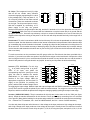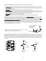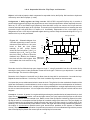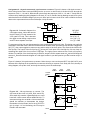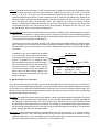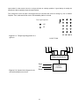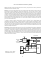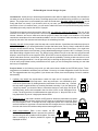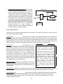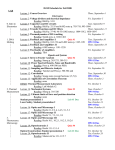
1
ELE 202
DIGITAL
CIRCUIT
DESIGN
LABORATORY
TABLE OF CONTENTS
Page Contents
2
3
4
8
12
15
17
26
30
32
33
Syllabus
Introduction
Lab 1. Basic Electronic Instruments and Measurements
Lab 2. Oscilloscope and Function Generator
Lab 3. Combinational Circuits: CMOS Logic Gates
Lab 4. Sequential Circuits: Flip-Flops and Counters
Lab 5. Electronic Design Automation with Mentor Graphics
Lab 6. Some MSI Chips and State Machine Design
Lab 7. Sequential Circuit Design: Automobile Taillights Control
Lab 8. Static Random Access Memory (SRAM)
Design Project. Introduction, Suggested Topics, and Project Management
SEMESTER
Fall 2000
INSTRUCTORS
Peter Swaszek, Ying Sun
DEPARTMENT
Electrical and Computer Engineering,
University of Rhode Island
Copyright © 1998-2000, University of Rhode Island
Course title
ELE 202 Digital Circuit Design Laboratory
Catalog
description
(I,1) Laboratory experience in digital electronics; logic design projects using standard
integrated circuits. (Laboratory, 1 credit)
Prerequisite
Credit or concurrent enrollment in ELE201
Text book
Laboratory manual, CMOS data book
Course
Objectives
To Understand – Know how to use basic electronic measurement instruments and
how to measure DC voltage, current, and logic states.
To Question – Consider alternative designs of digital circuits for solving engineering
problems.
To Design – Use SSI, MSI, LSI chips and software tools to design digital circuits.
To Lead – to participate in a team-based design project.
To Communicate – Learn communication skills through oral presentation, written
proposal, abstract, and final report for the project.
Laboratory
Assignments
1.
2.
3.
4.
5.
6.
7.
8.
Class/lab
schedule
Laboratory: 3 hours/week
Course
outcomes
1.
2.
3.
4.
5.
6.
Basic Electronic Instruments and Measurements
Oscilloscope and Function Generator
Combinational Circuits: CMOS Logic Gates
Sequential Circuits: Flip-Flops and Counters
Electronic Design Automation with Mentor Graphics
Some MSI Chips and State Machine Design
Sequential Circuit Design: Automobile Taillights Control
Static Random Access Memory (SRAM)
Knowledge of basic electronic instrumentation and digital circuits (a).
Skills of conducting experiments and building prototypes of digital circuits (b).
Ability to design digital circuits for solving specific engineering problems (c).
Consideration of alternative designs of digital circuits (l).
Ability to manage a design project with a small team (d).
Ability to identify, formulate, and solve an engineering problem with a statemachine approach (e).
7. Ability to conduct oral and written presentations of the course project in a
comprehensive but succinct way (g).
8. Ability to use software tools including schematic design and circuit simulation to
design digital circuits (k).
Assessment
Methods
1. Laboratory reports
2. Oral presentation of the project
3. Proposal, abstract, and final written report of the project
Relationship
of course to
program
objectives
This course contributes to Objectives 1 and 2 by equipping students with the
necessary background to work in digital circuit design.
Professional
component
Engineering science: 0.5 credit
Engineering design: 0.5 credit
2
INTRODUCTION
About the Labs
There are eight required laboratories for ELE 202. Lab 1 begins on Monday of the second week of the
semester. We will proceed at a pace of one lab every 1-2 weeks. The duration for each lab is specified in the lab
description that follows. Depending on the enrollment you will likely have one or two classmates as your lab
partners. You will work as a team on one of the six benches in the Digital Electronics Lab (Kelley 120). However,
each of you must submit individual lab reports without collaboration with others. Therefore, you should
understand every detail although you work as part of the team. Make sure that you record all the data and graphs
necessary for the report. A lab report will be prepared for each lab and due one week after the completion of
each lab.
About the ELE202 Recitation
You need to register for one of the ELE 202 recitation sessions, because the 1 credit goes with a recitation
session, not the lab itself. Starting from the fall 2000 semester the recitations will be used as office hours of the
teaching assistants and instructors to answer student’s individual questions.
About the Design Project
After you finish the eight required laboratories, you will apply the knowledge you have learned to a design project.
The project specification may read something like this: Design the control logic for a programmable electronic
lock. At the moment this may not make much sense to you. Hopefully around midterm you will identify a topic for
your project and begin to specify the steps towards solving it. The procedure and ideas for the design project will
be given and discussed in the ELE202 recitation sessions. The project will be conducted in five phases: 1)
proposal, 2) abstract, 3) oral presentation, 4) demonstration, and 5) documentation (written report).
About Electrical Safety
Improper connection of circuitry or
improper use of electronic instruments can
cause severe consequences including
damage of circuit components, damage of
electronic instruments, fire, injury, and
even death. The table on the right
summarizes the hazards caused by the
different levels of electrical current flowing
through the human body.
Current Through
Human Body (Amperes)
1
burns - 1~5 A
severe burns
breathing stops
death
0.1
0.01
extreme breathing difficulties
breathing upset
labored breathing
severe shock
muscular paralysis
cannot let go
painful
mild sensation
ventricular fibrillation
100~300 mA
maximum let-go
current -10 mA
maximum harmless
current - 5 mA
threshold of sensation
0.001
perception threshold 1 mA
Lab 1. Basic Electronic Instruments and Measurements
Object. In this assignment we learn to work with power supplies, voltmeters, ammeters, and ohmmeters. We
shall measure the V-I characteristic for a resistor, and the transfer characteristic for a TTL and a CMOS inverter.
We set up an LED voltage level indicator for CMOS chips. This lab should be completed in a session (1 week).
Power Supply. This supplies electrical power at a specified voltage across its terminals. This voltage may be
fixed or variable. For example the Tektronix PS503A on your bench has one pair of output terminals which
supplies power at 5-Volt and another pair whose output voltage can be adjusted between 0 and 20 Volts. The
PMC power supply is another voltage power supply available on our work bench.
Voltmeter. A voltmeter measures the voltage drop from the point to which its red terminal is connected to the
point to which its black terminal is connected. Tektronix DM502 digital multimeter can be used as a voltmeter with
the appropriate control buttons depressed. Suppose a voltmeter measures x Volts when connected across
points A and B. If we interchange the leads from the voltmeter which are connected to A and B then it will
measure -x Volts.
Ground. The "ground" in a circuit provides a voltage reference point at 0 Volt. The ground is usually
indicated by “GND” or one of the two symbols shown on the right. The ground terminal is usually
color-coded black. In some instruments there is a third terminal, the chassis ground, in addition to the
red and the black terminals. The chassis-ground terminal (sometimes color-coded green) connects to the metal
case of the instrument and to the ground of the electrical system in the building. Your have an option to tie your
circuit ground (black terminal) to the chassis ground (green terminal) or not. In some other instruments you don’t
have this option. The circuit ground is internally connected to the chassis ground. This means that the ground
terminal is connected to the case, and also, through the power cable, to the ground terminal of all electrical
power being supplied to the building. It is important to realize that if you are using such devices all points marked
ground are shorted together. There can be only one ground in a circuit.
In connecting together various grounded instruments and supplies we have to make sure that a power supply
never gets shorted, i.e., have its two output terminals connected together. In such a case we are asking the
supply for an enormous amount of power which might destroy something. All the supplies in the laboratory are
well designed and will turn themselves off or display a red light should such a contingency arise. However this
may not happen soon enough to prevent some damage, and in any case it is bad practice to have to rely on this
safety measure. The two output terminals of a power supp ly must never get directly connected together.
Supplies or instruments which do not have a grounded terminal are called floating. The same instrument may
have both grounded and floating inputs or outputs. For example the 5-V supply on the PS502 is grounded and
the variable supply is floating.
Circuit. If we connect an element across the power supply (Fig. 1-1a) a current flows in the circuit. Note that a
closed path is necessary for current to flow. In the diagram, for instance, the current flows from the supply to the
element along the lead, through the element, back to the other terminal of the power supply, through the supply
and so round again. The power supply maintains the voltage V across its terminals. The element now has a
voltage V across it, and a current I flowing through it. In this situation the element gets a power (P) from the
supply. The magnitude of P is given by:
P = V × I,
where P in Watt, V in Volt, and I in Ampere.
Ammeter. In order to measure the current in the circuit we have to cut into the circuit at A and B and insert the
ammeter as shown in Fig. 1-1b. The voltage at the red terminal of the ammeter has to be higher than the voltage
at the black terminal so that the current enters at the red terminal and leaves at the black terminal. If the ammeter
4
is connected the wrong way the needle will get deflected the wrong way and get damaged. Again if excessive
current flows through the ammeter it will get damaged. We will shortly be learning how to estimate the currents
which will flow in a circuit so that we can use the Simpson milliammeter on your workbench safely.
current
power
supply
element
Figure 1-1. Basic circuit
(a)
and
circuit
for
measuring voltage and
current (b).
A
PMC
power
supply
red
PMC
A
black
B
(a)
red
V
black
(b)
Panel Meters. You will have noticed that the power supplies have meters which measure voltage and current.
These are known as panel meters, and indicate the voltage at the supply terminals and the current passing
through the supply. They are not very accurate, but are very useful in giving a rough idea of where we are when
doing an experiment, especially in warning us when we are exceeding some rating.
I-V characteristic for a resistor. Connect the circuit shown in Fig. 1-1b above where the element is the
resistor (ask your lab instructor to get the proper resistor for this set of measurements). Before turning on the
power supply turn the control knob all the way counterclockwise so that the output voltage is zero (by doing this
we ensure that we will not get excessive current through the milliammeter when we turn the power on).
Gradually increase the voltage across the resistor, and measure the voltage across it for various values of the
current flowing through it. Take data up to the value 50 milliamperes. Whenever you take data it is good practice
to take it in neat tabular form so that it is absolutely clear what measurements were being made - label the
columns and rows, mark the units etc. It is also very good practice to plot your data on a graph as you take them
so you can see what is happening to the output as you change the input.
From your measurements it should be clear that the voltage across a resistor is proportional to the current
through it. This is the ubiquitous Ohm’s Law:
V = R × I,
where V in Volt and I in Ampere. R is called the resistance of the resistor, and the unit Volt/Ampere is called an
Ohm. Find the resistance of the resistor you worked with.
Power. We said that if an element has a voltage V across it and a current I flowing through it then it absorbs
power VI. Remove the ammeter from the circuit and have the power supply connected directly across the
resistor. (We are doing this to protect the ammeter). Gradually increase the voltage to about 8 or 10 Volts and
then feel the resistor. It is evident that the power absorbed by the resistor generates heat in it. (If you put on too
high a voltage you might burn out the resistor, which is why it is suggested that you do this gradually).
Ratings. All elements will have some power, voltage, and current ratings. In designing with these elements we
will have to bear these values in mind and see that they are not exceeded. For example the resistor you worked
with is a 1/2 Watt resistor, which means that the resistor can handle a maximum power dissipation of 1/2 Watt.
Multimeter. Measure the resistance of the resistor you used with the ohmmeter. The DM502 digital multimeter
can be used as a voltmeter, an ammeter, or an ohmmeter by dialing to the appropriate function and range.
However do not use the instrument as an ohmmeter in a live circuit, i.e. a circuit with a power supply. Note also
that you cannot leave the instrument in the circuit and change its operation from measuring voltage to measuring
current by depressing the appropriate control button. Voltage is measured across an element current flows
through an element.
5
IC Chips. The integrated circuit (IC) chips
1
14
16
1
24
that we will use contain many elements 12
2
2
23
13
15
3
connected together and packaged in a dual 3
22
3
12
14
4
21
4
11
13
in-line package (DIP). They may have 12, 14, 45
5
20
5
10
12
6
19
16 or 24 pins to which we can make external 6
6
9
11
7
18
7
7
8
10
8
17
connections. These are numbered as shown
8
9
9
16
on the right. The chips need power to work,
10
15
14
11
and this is supplied by connecting a 5-V
12
13
power supply to the chip, the ground
terminal of the supply to the ground pin of the chip, and the 5-V terminal to VCC or VDD pin as the case may be. In
most (but not all) cases if the chip is mounted with the indentation on top the bottom left pin is ground and the
top right is VDD or VCC . One sure way to destroy a chip is to connect it backwards, so be sure to check the pin
diagram of the chip before turning on the power. In all our work with chips we shall work only in the range from 0
to 5 volt .
Protoboard. To make it convenient to build circuits with many IC's we have the protoboard on which the chips
can be mounted. Use the ohmmeter to discover the internal connections in the protoboard. Notice that the chips
go in straddling the vertical channels in the board. In putting the chips into the protoboard or in taking them out
do not use force. This is another sure way of destroying chips. The pins get bent and the chip is useless. Always
use the insertion and extraction tools which are on your bench (if you are not sure the lab instructor will show you
how to use them).
To make connections on the protoboard use #22 gauge solid wire. Each bench has been provided with a
selection, if you need more there are spools of wire and a wire stripper on the back bench. Always take a little
care in using the board. If a pin or a wire breaks off inside the socket it is very hard to take out, and the socket is
ruined. A little practice in using the board is very helpful, do not let your lab partner do all the assembling!
7404
14049
16
Inverter (TTL S N 7 4 0 4 ) . For this chip
1A
Vcc
VDD
NC
13
15
2
2
V CC is at pin#14 and ground is at pin#7.
1Y
6A
1Y
6Y
12
14
3
3
Pin#1 is an input, and pin#2 the
2A
6Y
1A
6A
11
13
4
4
corresponding output etc. (see figure on the
2Y
2Y
5A
NC
right). We want to measure the transfer
10
12
5
5
3A
2A
5Y
5Y
characteristic, i.e., the output voltage as a
9
11
6
6
3Y
3Y
4A
5A
function of the input voltage. Make the
8
10
7
7
GND
3A
4Y
4Y
appropriate connections. Use the fixed 5-V
9
8
Vss
4A
supply on the PS503A for providing the
power, and the PMC variable voltage source
for supplying the input voltage. Measure input and output voltages with the DM502 multimeter. In taking the data
you will find it useful to graph the points as you make the measurements. You might run over the range in big
steps first, and then examine the places where things are changing rapidly by taking finer steps in that range.
1
14
1
Inverter (CMOS MC14049). The pin connections for this chip are not the same as for the 7404 (see figure
above). Graph the transfer characteristic for this inverter. Power up this chip by connecting VDD to 5 volts and
Vss to ground. (Note that the labeling for the power and ground pins is related to the semiconductor technology:
V CC – collector of a TTL transistor, VDD – drain of a MOS transistor, and VSS – source of a MOS transistor.)
It is clear why these chips are called inverters. A low voltage at the input produces a high voltage at the output,
and a high voltage at the input produces a low voltage at the output. Actually these are called hex-inverters
because there are 6 inverters in each chip, the pins 1,3,5,8,10,12 being the inputs, and pins 2,4,6,9,11,13 the
6
corresponding outputs. From your measurements on each chip find the points at which the transfer
characteristic has unity gain. These are the points at which ∆V out is equal to ∆V in. On the graph they are the
points at which the slope of the transfer characteristic has unit magnitude. We shall use these observations later
when we consider noise margins for different families of IC chips.
Designing a logic level indicator. In digital circuits we deal with binary signals (i.e. logic 0 and logic 1) most
of the time. So it would be convenient to devise a simple indicator to show the logic level of a signal. We can use
a Light Emitting Diode (LED) for this purpose. The LED emits light when a current flows through it, entering at
the + terminal (P) and leaving at the - terminal (N). The LED’s we use in this lab usually have a maximum current
rating of 100 mA.
The indicator on the protoboard can then be set up as shown on
test point
5V
VCC
the right. When the voltage at the test point is 0V there is no
current flowing through the LED and it is OFF. When the test
1
voltage is 5V the LED is ON. Choose the appropriate value of
R
the resistance R, set up the indicator. The resistor R limits the
2
current through the LED. Without it the LED would burn out
+
immediately. A 220-Ω resistor would limit the LED current to LED
7404
about 20 mA. Can you confirm this with Ohm’s law? Assume that
the voltage drop across the forward-biased LED is about 0.7
volts. You can make the LED brighter (dimmer) with a smaller (larger) resistance. But do not go over the 100-mA
limit. Notice that we use the TTL inverter (7404) instead of the CMOS inverter (14049). Although the CMOS
inverter has good voltage transfer characteristics as shown earlier, it is not capable of supplying enough current
to drive the LED. The TTL inverter on the other hand can sink a high current when its output is low. Use this LED
indicator for the next part of the lab.
Two coupled inverters. In the CMOS inverter chip if the output of one inverter is connected to the input of
the second, and the output of the second to the input of the first (see Fig. 1-2a), what do you expect will be the
voltages at the various pins? Try to work out what they will be, and then do the measurement to find out if you
were right. Notice that the TTL inverter won’t work in this case. Use the LED indicator in the previous step to
check the output in the coupled inverter circuit.
Three coupled inverters. Now set up a coupled circuit with three inverters, i.e. the output of the first is the
input to the second, the output of the second is the input to the third, and the output of the third is the input to
the first (see Fig. 1-2b). Check the voltages with your indicator. If your circuit works properly, you should observe
that the LED is on but appear to be much dimmer than usual logic-1 state. Can you explain this?
Figure 1-2. Schematic diagram for two
coupled inverters (a). Touch the input
wire momentarily to 5V (GND) to register a
1 (0) and then let the input floating. For
three coupled inverters (b) do not tie the
input to either 5V or GND.
(a) 5V
Test point
(b)
Test point
Lab report. A written report for this lab will be due a week from the day you do the lab. The report is intended to
be a technical documentation for the lab performed. I f you give your report to someone who has not done the
lab, you would expect him or her to duplicate exactly what you have done according to your report. The report
doesn’t have to be long; it should be concise and sufficiently comprehensive to address all the questions,
observations, results, and designs in the lab. The report should be neat and well organized. If your hand writing
is not very legible, you should prepare the report with a typewriter or, more preferably, a word processor. Consult
your lab instructor for the specific format of the report.
7
Lab 2. Oscilloscope and Function Generator
Object. In this assignment we learn to work with the oscilloscope and the function generator. We display the
transfer characteristic of an inverter and measure the time required for a signal to propagate through the inverter.
We use the function generator and the oscilloscope to study the input-output relations of the CMOS AND gate
and OR gate. (1 week)
The Oscilloscope. This is an instrument you will be using very often. The chart hung up in the back of the
Laboratory gives you a first lesson in using the oscilloscope. The operator's manual for the oscilloscope is in the
folder on your bench. The following steps are suggested as a way of getting started, once you complete them
you should proceed to do more measurements on your own so that you get familiar with every control on the
instrument. The following description is for the Tektronix 2215 60 MHz oscilloscope. The Tektronix 2235A 100
MHz oscilloscope is very similar. If you have another type of scope on your bench, the description of the frontpanel controls may not be accurate but the basic operation should be the same. Please note that we are in the
process of up grading the oscilloscopes. If you have a different (newer) oscilloscope on your workbench, the
specific instructions pertaining to the oscilloscope may not apply, but the general principle remains the same.
Getting Started. The controls can be divided into four sections - the display, the vertical, the horizontal , and
the trigger system controls. Turn the power on. You should see a horizontal line on the display. If there is none,
depress Beam Finder and position the blob in the center of the screen with the vertical position knob above CH1
and the horizontal position knob above HORIZONTAL MODE. Then release Beam Finder and you should have
the trace. If not ask for help from instructor.
Display System Controls. Use the intensity, focus, and vertical and horizontal position knobs. At all times
the scope should have a clear well focused trace which is just bright enough to be seen with comfort. The trace
should never be too bright with a surrounding glow, this decreases the life of the display. You should never have
a bright stationary spot on the screen . This burns the spot in and ruins the display.
Horizontal system controls. Move the sec/div knob step by step CCW till you are at .2 second. You may
have to adjust the intensity and focus controls to keep the display in focus with the right brightness.
In this setting we see that the display is actually a spot. The horizontal system moves the spot from left to right
across the screen at a speed given by the sec/div control knob. This control is called the sweep generator; with
the setting of .2 s on the sweep generator the spot moves across the ten divisions on the screen in two
seconds. When the spot reaches the right edge the horizontal system pulls it back in the retrace period, the spot
stays in the left for a holdoff time, and then repeats the cycle. During retrace and holdoff we do not see the spot
because the display system blanks it out.
Note the tremendous range of the sweep generator. With one turn of a knob, we can measure the time interval
between events which occur 5 seconds apart and events which occur 50 nanoseconds apart. In order to do this
we have to make the spot mark the instant at which the first event occurred and the instant at which the second
event occurred. This can be done by coupling signals from the events into the vertical system. This system
deflects the spot in the vertical direction. The distance between the vertical jumps on the screen will be
proportional to the time interval between the two events.
Vertical System. Coupling the input signal to the vertical system is done through the BNC connector at the
bottom of the channels. In the BNC connector the signal is carried by the central pin, and the sleeve is ground.
The oscilloscope is a grounded instrument. You could connect the scope to the circuit under test with just a wire,
but this is to misuse the instrument. The connection would load the circuit in an unpredictable fashion, the wire
would act as an antenna and pick up stray signals, and the scope would not be able to perform to its full capacity.
Connecting input signals to the vertical system is always done through a probe.
8
The Probe. The probe consists of a resistive cable and a grounded shield. In order to put the signal into the
scope connect the probe to the channel input with the mating BNC connectors. Note that in making this
connection you have to press in and then rotate CW to lock the connection in place.
Some of the probes have a 1X and a 10X adjustment. In the 10X position the signal is attenuated by a factor of
ten before being fed into the scope. In this assignment we use the probe in the 1X configuration.
The end of the probe has a spring connection with which you can clip the probe to a wire carrying the input
signal. This clip is delicate, do not try to force it to grab binding posts etc., it is just meant to be clipped around
wires. In case you want to get the signal from the pin of an IC chip you can remove the top plastic sleeve on the
probe. This will expose the probe tip, which can then be pressed on the pin to acquire the signal. In this case, of
course, you have to keep holding the probe in place.
The ground clip at the end of the probe has to be connected to ground. If it is not long enough to reach a
grounded point in your circuit then extend your circuit, do not try to stretch the ground lead on the probe. It will
get pulled off and will have to be mended.
Vertical System Controls. Let us put a simple signal into the vertical system of the scope. Connect the BNC
end of the probe to CH1. Set the selection switch on the probe to 1X. Connect the other end of the probe
across the output terminals of the variable voltage supply on the PS503A. (Remember what we said about
clipping the probe on. Connecting short bare wires to the output terminals of the power supply will help you
attach the probe properly).
Set the sweep generator at .5 ms/div ; at this setting you see a nice horizontal trace with no flicker, which makes it
comfortable for the eyes. Set the CH1 VOLTS/DIV at 1 on the 1X indicator; since we are using the 1X setting on
the probe it means one vertical division corresponds to one volt. Set the selector switch above the knob to CH1.
With the selector switch below the knob set at GND use the vertical position control knob to set the trace along
the bottom dotted line of the display.
Now switch the selector from GND to DC and vary the output of the PS502 variable voltage supply. You can see
that the vertical deflection is proportional to the voltage at the CH input. Use the VOLTS/DIV knob to change the
vertical scale. Note that with the 1V scale the reading from dotted line to dotted to dotted line on the display is 5
Volts.
The Function Generator. To get a slightly more complicated signal into the scope let us try to use the
function generator FG503. Note that the output is not grounded, if you look carefully you will see the insulation
between the sleeve of the connector and the case. Use the oscilloscope to monitor the output of the FG503.
You can connect the oscilloscope and the FG503 by use of the proble or simply a direct BNC-to-BNC cable. The
setting of the oscilloscope is the same as before except sweep generator at 50 µs. Adjust the front-panel control
of FG503 to generate a 0-5 Volt square wave of 10 KHz. You should see a square wave on the display. If you do
have a problem getting the trace you might try adjusting the level knob in the trigger section. If you still have a
problem get the instructor to help.
Trigger Section Controls. Set up the function generator and scope to see 5V pulses of 100 µs period on
the display. Set the sweep generator at 50 µs so we see a few pulses.
Now turn the level knob in the trigger section all the way CCW and notice what happens. Get the steady picture
back again by going back to the previous setting. Turn the A&B INT switch to CH2 and see what happens. Set
the switch back to CH1. Set the source to EXT and see what happens. This time, instead of going to the old
setting, take a BNC to BNC cable and connect it from the TRIGGER OUT of the FG503 to the EXT input of the
trigger section of the scope. See what happens.
9
Obviously something gets out of synchronization.
Let us think out carefully what is happening. The spot starts on the left and moves to the right at a speed set by
the horizontal sweep. In this case it is taking 50 µs times 10 divisions, i.e. 500 µs to get across. During this time
the vertical position depends upon the voltage at the CH1 input. If this goes up and down, the spot goes up and
down. Thus the oscilloscope draws a graph of voltage versus time on the screen. But note that the graph is all
done and complete in 500 µsec.
Now what does the spot do. It is retrace and holdoff time, during which it is blanked out and gets to the left of the
screen . This takes some time - it is not accurately fixed but depends on the settings and will probably have a little
jitter in it. Then the sweep starts again, the spot starts moving from left to right and traces out a second graph.
With the settings we have the spot is drawing about 2000 graphs in a second. If we are to see a steady picture on
the screen it is obviously essential that the spot draw the same graph every time.
(1) This means the signal must be a repetitive one, i.e. the signal waveform repeats itself as time goes on.
(2) The spot starts drawing the graph starting at an equivalent point on the signal shape each time around, i.e.,
the starting of the sweep must be synchronized with the starting of the repetition of the signal.
This last condition is achieved by the trigger controls. When the blanking period is ended the spot does not start
till it is told to do so by the trigger.
In our first setting the SOURCE to the trigger was INT. This tells the trigger to look at INT. There the switch was
set at CH1. The trigger then takes the signal which is coming into CH1. The slope and level settings tell the
trigger to operate when this signal has reached such and such a level and is increasing. At this instant the trigger
starts the spot on its trace. By this means we got a steady picture of the shape of the signal.
In the last exercise we used an external signal to tell the trigger when to act. That signal came from the FG itself,
which sends out trigger information synchronized with its pulses.
Dual Channel Vertical System Controls. The scope has two input channels for the vertical system. So far
we have used only channel 1; we could just as well have used channel 2, as both channels are similar. It is also
possible to have two input signals and use both channels simultaneously. For example we can apply a signal to
the input of an inverter and look at both the input and output waveforms. The input can go into CH1 and the
output to CH2. Set up the FG to give 5V 100 µsec pulses with period 200 µs.
Before going ahead with the next step it
might be wise to turn off the power on the
instruments so that we do not accidentally
apply the wrong voltages when we are
setting up the connections shown on the
right.
PG
PG
Signal
Probe 1
Clip
PS
Probe 2
Clip
VDD
IN
PS
OUT
CHIP
GND
Note that when shielded cables are used
Scope
Outer
GND
GND
GND
GND
(as in the probes for example) there are
Sleeve PG PS
Chip
Probe 1 Probe 2
only short stretches of wire at the output
end. The reason for this is obvious; if you Probe 1 Probe 2
are going to great pains to have the signal go along a shielded path so that it does not pick up noise, you want to
keep the exposed portions as short as possible. Note also the number of leads which are attached to ground.
10
From these considerations it is clear we must pay attention to having good solid GROUND connections near our
circuit input and output terminals. You may find it convenient to have short bare wires and connectors which give
you GROUND in your circuit.
Set the vertical mode controls as follows - the left switch to BOTH (which activates the right switch) and the right
switch at ALT. Set both selector switches at the bottom to DC. You can trigger from CH1. You should see both
the input and output signals as the spot will be drawing them alternately on the screen. Work with the other
positions of the controls to learn what they do.
The Oscilloscope. The above set of exercises are just to get you started using the oscilloscope as a multi
purpose tool. There are many features we have not even touched upon like AC coupling, delayed sweep,
normal and TV triggering. As with all instruments the more intelligent practice you put in the greater your mastery
of the tool.
Inverter Transfer Characteristic. In Lab #1 we measured the transfer characteristic of an inverter point by
point, and plotted the results on graphs. The oscilloscope has a special x-y mode which should allow us to plot
the transfer characteristic curve directly on the display of the oscilloscope. Depending on the model of the
oscilloscope, the x-y mode is usually selected by turning the time-resolution knob all the way counterclockwisely.
But be careful not to leave a stationary bright spot on the display. When there is no input in the x and y (channel 1
and 2), the electron beam remains stationary at one spot. If this happens you should immediately move the spot
off the screen using the position knobs or turn the intensity to a very very low level. A better way to do this is to
leave the time-resolution knob on the normal two-channel mode when you set up the inverter circuitry and turn
to the x-y mode when all signals are available and applied to the oscilloscope.
To plot the transfer characteristic of an inverter, set the function generator to “sweep” the 0-to-5 voltage range.
The triangular waveform should be appropriate for this purpose. This 0-5 volt triangular wave is sent to the input
of the inverter and also to channel 1 (x axis) of the oscilloscope. The output of the inverter is sent to channel 2 (y
axis) of the oscilloscope, therefore creating an “electronic” plot of the curve just like what you did on paper in Lab
#1. You will need to adjust the position and voltage scale on channel 1 and 2 for proper visualization of this
curve.
Plot the transfer characteristics with the oscilloscope for both the TTL and CMOS inverters (7404 and 14049). A
more advanced digital oscilloscope may have an interface to a printer or a plotter for direct screen dump. Since
we don’t have such setup in the lab yet, you need to sketch what you see on the oscilloscope on paper and put
it in your lab report.
For each of the transfer characteristic curves you may notice that there are two traces slightly apart from each
other. This should be particularly noticeable for the TTL 7404 and is due to the fact that the interver output is
slightly different when the input is swept up (0 to 5 V) and down (5 to 0 V). The phenomenon is analogous to the
hysteresis typically observed in electromagnetics. It is usually frequency-dependent. Change the frequency of
the function generator and observe its effect on “hysteresis.” Briefly describe your observation in the lab report.
11
Lab 3. Combinational Circuits: CMOS Logic Gates
Object. In this assignment we study the basic logic gates: AND, OR, NAND, and NOR. We design and realize
some simple combinational logic circuits by using these gates. (1 week)
Proto-Board PB-503. The proto board has built-in power supplies. We shall be using only the fixed 5V
supply. Use the multimeter to discover the internal connections and operation of the board. Remember that one
should not use an ohmmeter in a live circuit. Note also that the voltmeter might give any reading between 0 volt
and 5 volt when used to measure the voltage drop across a floating point and ground.
CMOS logic levels. As you have seen in ELE201 there are only two logic levels: 1 and 0. With the power
supply (V DD ) at 5 Volts the voltage at any input or output in CMOS digital circuits will be either 5V or 0V. So let us
agree on the convention that 5V level corresponds to logic 1 and the 0V level corresponds to logic 0. This
convention is called positive logic. Some logic systems, such as the popular PDP-11 computers back in the
1970’s, actually use the negative logic convention, which means that the higher voltage corresponds logic 0 and
the lower logic corresponds to logic 1. But let’s not confuse ourselves here. We will use positive logic
convention throughout the rest of this course. So instead of talking about voltages in the circuit we shall talk
about logic levels. A two-input CMOS gate has two inputs and one output. The output level is a function of the
two input levels.
IC Chips. We shall be working with the following chips:
14001 Quad 2-input NOR gate
14011 Quad 2-input NAND gate
14070 Quad Exclusive OR gate
14071 Quad 2-input OR gate
14077 Quad Exclusive NOR gate
14081 Quad 2-input AND gate
“Quad 2-input” means that each chip contains four identical gates which perform the same logic function and
each gate takes 2 input signals. The pin connections are the same for all these chips.
V DD (5V)
V SS (Ground)
Inputs
Inputs
Inputs
Inputs
pin 14
pin 7
1, 2
5, 6
8, 9
12, 13
Output
Output
Output
Output
3
4
10
11
We want to find out the logic function performed by the gate in each of the different chips. Since the four gates
in a chip are identical it is only necessary to make measurements on one of them per chip.
Assignment 1: Basic Gates. We want to set each input to 1 or 0, for each of these conditions we want to
see if the output is 1 or 0. The obvious thing to do is to set up our LED logic level detector at the output and
arrange to apply the proper input states. The first assignment of this lab is to complete the following truth table.
Input
A B
0
0
1
1
AND
OR
Output
NAND NOR
0
1
0
1
12
XOR
XNOR
This is quite easy for this particular assignment, but let us start learning some good design rules now.
Wiring the Protoboard. In all digital design projects it is essential that all wiring be neat and orderly. It must be
immediately obvious what the interconnections are on the protoboard; "rat's nest" wiring is not permitted. The
following suggestions are helpful:
1. Mount all chips with the indentation on top. This might lead to lengthier wires in some cases, but the ease of
identifying pin numbers at a glance makes it well worth while.
2. If possible avoid running wires over a chip, it makes it hard to insert and extract the chip.
3. On each side of the central channel on which the chips are mounted there are two vertical strips of
connected sockets. Use the outer two to run the VDD line and the inner two to run the ground line. The little
U-shaped wires you have on your bench enable you to connect a pin to VDD or GROUND neatly.
4. Use red wires for connecting to VDD , black wire for connecting to GROUND. Use yellow wire for the signal. In
some designs you may want to distinguish one set of signals from another, for example you may want one
set to be input and another set to be output. In this case you may want to use yellow, blue, and/or purple
wires for your signals. Later we will be using a clock, use white wire for clock signals.
5. Whenever possible use short connections which lie along the protoboard. However do not hesitate to use
longer connections if it will make it easier to follow the signal flow through the system.
6. You will find the longnosed pliers very useful in inserting and extracting connecting wires. There are spools
of wire and a cutter and stripper on the back bench.
Measurements. We want to be able to switch from 1 to 0 at the inputs. We can do so with the flick of a switch.
On the proto board we can use the DIP switch S1 and the single-pole-double-throw (SPDT) switches S2 and S3.
To generate the logic 0/1 signals, the DIP switch or the SPDT switch need to be wired to 5V and ground. Study
the following diagrams.
(a) SPDT switch
(b) DIP switch with
pull-up resistors
(c) DIP switch with
pull-down resistors
5V
5V
10KΩ
10KΩ
logic 1 (0)
Figure 3-1. Wiring of DIP
switch and SPDT switch for
generating logic signals.
to gate
input
5V
Notice that pull-up or pull-down resistors need to be used with the DIP switch. Otherwise, a short circuit (5V
directly to ground) would occur and damage the proto board. Depending on how many input signals you need,
you can wire up S2 and S3 without resistors to provide 2 inputs, or you can wire up S1 with resistors to provide
up to 8 inputs. For output you can either set up the LED logic level detector in Fig. 1-3 or you can simply use one
of the 8 LED indicators on the proto board.
Since all the 6 chips under testing have the same pin assignment, the same wiring can be used for all chips. Each
time when you move on to another chip, just carefully lift the chip and insert the new one without disturbing the
wires. Once the wiring is done, it should take only a few minutes to run through all the chips.
13
Designing Combinational Logic Circuits. The general procedure is as follows:
1. Specifications: Understand the problem and make sure the problem can indeed be solved by use of a
combinational circuit. Identify and assign symbols to the logic variables. Specify them as inputs and outputs
of the combinational circuit.
2. Truth table: Assign logic levels to the outputs for every combination of the inputs.
3. Logic functions: From the truth table derive the logic functions. Express every output as a function of the
input. Simplify these logic functions by use of Boolean algebra, Karnaugh map, or computer software. The
Karnaugh map (K map) will be the most frequently used technique in this course.
4. Prototyping: Implement the circuit on the proto board.
5. Testing: Measure the input-output relations and validate the circuit against the original truth table.
Assignment 2: Design of a seat-belt warning buzzer. Problem statement: Devise a gate circuit to
sound a warning buzzer in an automobile if the ignition key is ON and either the driver's seat belt D is not buckled
or the passenger's seat belt P is not buckled and a pressure switch S indicates that that seat is occupied. Build
and demonstrate the working of this circuit. The output of the buzzer circuit can be connected to an LED
indicator on the proto-board. Or, to make it more dramatic, use the speaker driver circuit as shown in Fig. 3-2.
Notice that an open-collector TTL NAND gate (7403) is used instead of a regular TTL NAND gate (7400). See
below for a brief explanation of “open-collector.”
5V
Function Generator
on Proto-Board
TTL Output
Figure 3 - 2 . A logic indicator circuit by use of the function
generator and the speaker on the proto board.
7403
Test Point
Open-Collector Circuitry. The TTL7403 is a quad NAND gate IC with open-collector circuitry. Its pin
assignment is shown below. Also shown is a simplified circuit for the typical output stage of a TTL logic gate. The
circuit consists of a load resistor, a diode for protection purpose, and a PNP transistor. In the case of a opencollector gate the internal load resistor is absent, allowing the designer to add an external load (the speaker in
this case).
Vcc
7403
1A
1B
1Y
2A
2B
2Y
GND
1
14
2
13
3
12
4
11
5
10
6
9
7
8
Vcc
Logic 0/
Logic 1
4A
4B
C
B
4Y
E
3A
3B
Logic 0/
Open circuit
B
E: Emitter
B: Base
C: Collector
C
E
3Y
Simplified
typical TTL
output
14
Open-collector
TTL output
Lab 4. Sequential Circuits: Flip-Flops and Counters
Object. In this lab we learn the basic component for sequential circuits, the flip-flop. We learn how to implement
counters by use of the D flip-flops. (1 week)
Assignment 1: Shift register and ring counter. MC14175B is a quad D flip-flop chip. It contains 4
positive-edge-triggered D flip-flops with asynchronous reset. Study the specification sheets especially the truthtable on p. 6-197 of the CMOS Logic Data book. Note that there is only one common clock input and one
common reset input which apply to all 4 flip-flops. The reset input is asynchronous active-low. Asserting the reset
input with a logic 0 will reset all the Q outputs to 0 immediately, independent of the clock signal. In this
assignment we use a 4175 chip to implement register and ring counter. Study the schematic diagram in Fig. 4-1
and then wire it up on the proto board.
LED logic indicators
5V
Figure 4-1. Schematic diagram for a
3-bit shift register/ring counter. Use the
debounced push-button on the proto
S1
board to enter the clock pulses
S2
manually. (A 10KΩ pull-up resistor
should be used as shown.) Use S 1 to
introduce logic 1 to D0. Use S2 to reset
the circuit. Use S3 to close or open the
feedback loop. Without the feedback Debounced
the circuit acts like a shift register. With push-button
the feedback the circuit acts like a ring
counter.
S3
4
2
D0 Q0
5
7
D1 Q1
C
C
12
10
D2 Q2
C
Reset 1
5V
MC14175
10KΩ
Clock 9
VDD 5V pin 16
VSS GND pin 8
Reset the circuit first. With the loop open, deposit a single “1” using S1 and shift it from Q0 to Q1 and to Q2 by
entering the clock pulses via the push-button. Reset the circuit again. This time try to deposit two 1’s and shift
them to the right. This circuit is a shift register.
Reset the circuit. Deposit a 1 and shift it to Q0. Now close the loop with S3 and rotate the 1 around the loop.
Repeat the exercise with two 1’s in the loop. This circuit is called a ring counter for obvious reason.
It is import that you use a debounced switch to enter the clock. The glitches from the mechanical vibrations of the
switch are eliminated by a switch-debounce circuit to ensure a single pulse from each depression of the button.
Without the switch debounce circuit, multiple pulses will be generated from a single depression and you won’t
be able to control the operation. You can replace the debounce push-button with just a switch and see what
happens.
Counters. A counter, in general, is a register which goes through a prescribed series of states driven by a clock
signal. For an asynchronous counter, such as the ripple counter, the clock inputs of the flip-flops are not driven
simultaneously from a common external clock. Rather, some of the flip-flips are clocked by outputs from other
flip-flips or itself. As a consequence all the flip-flops do not switch exactly at the same time. They are slightly out
of synch because the accumulation of delays through the chain of flip-flops results in a ripple effect of the
switching. The accumulated delay slows down the circuit, and might also cause timing problems and glitches in
the outputs. A synchronous or parallel counter gets around these problems at the expense of additional
circuitry. The basic principle of operation of synchronous counters is to use combinational logic with the present
state of the flip-flops to present the correct input at each flip-flop for its next state.
15
Assignment 2: Asynchronous and synchronous counters. Figure 4-2 shows a 2-bit ripple counter in
which A1A 0 gives the down count and B1B 0 gives the up count. In other words, A1A 0 should cycle through the
sequence of 00, 11, 10, and 01; B1B 0 should cycle through the sequence of 00, 01, 10, and 11. Study how the
circuits work by drawing the timing diagram for the clock, A1, A0, B1, and B 0. Start by drawing several clock cycles
and show how A1A 0 and B1B 0 change cycle-to-cycle. Wire up the counter circuit. Drive it with a 100KHz clock and
observe the output waveforms on the oscilloscope. Verify the result.
5
1
A0
D0 Q0
3
Clock
C
2
B0
MC14013
D-FFx2
Figure 4-2. Schematic diagram for a
2-bit ripple counter. Notice that we use
the 4013 dual D-FF chip instead of the
4175 quad D-FF chip. This is because
the ripple counter design requires that
each FF has a separate clock input.
9
13
11
Reset (4, 10) = 0
Set (6, 8) = 0
VDD (14) = 5 V
VSS (7) = GND
A1
D1 Q1
12
B1
C
To save some wiring time, we demonstrate the ripple counter design with only 2 bits. This design can easily be
expanded to more than 2 bits. With the inverted terminal fed back to the input each flip-flop acts like a toggle flipflip (T-FF); the output toggles its state on every positive edge of the clock pulse. The external clock drives the
first flip-flop. The output of the fist flip-flop (Q0) drives the clock input of the 2nd flip-flop. We can keep on
extending this ripple effect for more than 2 flip-flops. The ripple counter also acts like a chain of frequency
dividers. For example, if the clock frequency is 100 KHz, we get a 50 KHz square wave at A0 and a 25 KHz square
wave at A1. Draw the schematic diagram of a 4-bit ripple counter in your lab report but you don’t need to verify it in
the lab.
Figure 4-3 shows a 3-bit synchronous up counter. Notice that you can use the quad D-FF chip (MC14175) now
because all the flip-flops in the synchronous counter are driven by a common clock. Study the circuit, develop a
timing diagram, wire up the circuit, and verify the result by use of the oscilloscope.
4081
ANDx4
Counter
enable
E
4070
XORx4
1
4175
D-FFx4
3
4
2
1
D0 Q0
2
A0
C
2
3
5
4
5
6
5
Figure 4-3. 3-bit synchronous up counter. The
chip count of this circuit is 3 (4070, 4081, and 4175).
Since each chip contains 4 gates/flip-flops, we could
have built a 4-bit counter without additional chip. To
save some wiring time we build a 3-bit counter which
should be sufficient to demonstrate the design.
Remember to tie the Reset* line for the 4175 D-FF’s
(pin 1) to logic 1. If it is left floating, the FF’s may be
locked in the reset state.
D1 Q1
7
A1
C
6
4
8
8
10
Clock
16
9
10
12
9
D2 Q2
10
A2
C
9
Output
carry
Lab 5. Electronic Design Automation with Mentor Graphics
Object. In this assignment we learn to use electronic design automation (EDA) tools for designing digital
circuits. Digital circuits are input to the computer by schematic capture software. Circuit behaviors are determined
by computer simulation using a hardware description language called VHDL. (2 weeks)
Object. The main objective of this lab is to become familiar with the ELE department's UNIX computing
environment, and to gain experience with the Mentor Graphics system's logic timing/functional simulator.
Additionally, you will design and simulate a basic counter, namely a Decade Counter, using the Mentor Graphics
software package. The knowledge you gain from this lab will be immediately utilized in the next lab when you first
simulate your design solution before actually building it.
In the following, Section I introduces you to the ELE system, Section II provides a brief tutorial to get you going
with four of the Mentor Graphics programs, and Section III has the details on the Lab 5 assignment itself.
I. Getting Started.
By this time you should have an accounts on the ELE computing systems. The main place to work is in the ELE
computing lab, located on the first floor of the Kelley Hall room 115. This is also possible to use the Engineering
Computer Lab (ECL), located in the new Kirk building. The Mentor Graphics software resides on the ELE
computer system. It is therefore a little bit more complicated to access the software from ECL via the network.
The following assumes that you are in the ECL; the differences with Kelley 116 will be noted. Most likely you will
finish this lab completely on the ELE computer. But it is helpful to know how a complex software system like
Mentor Graphics can be run over the network.
Most UNIX programs will also work on character-based terminals, i.e., over the phone lines, but many, including
our Mentor Graphics CAD tools, need to be run on workstations.
Setting Up Your Directory System. To begin with, read the Introduction to ELE Computing document
distributed in the lab by your TA or professor. Follow the instructions for logging-in given in that document. Note
that the instructions handed out are for your ELE account, not your ECL account; the procedure for ECL is
basically the same.
Now that you've read the Introduction to ELE Computing document, there are a few things you should do to
setup your account to make life easier on yourself. The following steps should only be done ONCE. The next
time you login, everything will operate as it should.
Directory Setup. You need to make a structure to hold your designs for ELE 202. Start by giving ELE 202 it's
own subdirectory off of your root directory. Type the following:
cd
mkdir ele202
at the Unix prompt. Note that on the ECL computers, you may need to open an xterm window first before you
can type commands, since the xterm window may not appear on the desktop by default. To open an xterm
window, click the right mouse button anywhere on the desktop and choose xterm from the pull-down menu.
Now we'll set aside a place where your files for this lab will be stored. First, change to the ele202 directory by
typing the following:
cd ele202
ls -a
There should be only two lines shown, one with the subdirectory “.”, and one with the subdirectory “..”. Actually,
these are not really subdirectories; in UNIX command syntax, a single period refers to the directory you are
17
currently in, and the double period refers to the parent directory of the one you are in. You should now be able to
make a directory for lab 5; name it whatever you want (e.g., lab5). Hint: just use a mkdir command.
ECL Environment Setup. Mentor Graphics requires that the path is modified and certain environment
variables are set in order to function properly. On the ELE system, these parameters are automatically set for you
whenever you log in; however, on the ECL system, you need to specify the file which includes all of these
modifications. The following steps must be done for the ECL system only.
1. From your ECL home directory, type: <editor> .cshrc ...where <editor> represents your favorite text
editor, such as emacs, vi, xedit, etc.
2. Add the following line near the end of the .cshrc file: source /tmp_mnt/lev1/.mgstart
3. Save the file and exit your editor.
4. Log out then log back in, or simply type: source .cshrc at the Unix prompt to update your system
environment variables. You are now ready to start running the Mentor Graphics Tools.
Please adhere to the following rules:
•
•
•
Rule 1: Every component for lab 5 should be in the lab5 directory that you just created.
Rule 2: All components should be at the same directory level, i.e., this is a “flat” directory structure, even
though logically your design is a hierarchy of components.
Rule 3: Except in certain noted cases, ALL manipulations of your lab5 directory and its contents should be
made ONLY within a Mentor CAD tool (usually Design Manager [dmgr]). This is true of ALL Mentor designs
and their parent directories.
Note: If you do not follow Rules 1 through 3, the Mentor tools may get confused and may not work right, and you
may thus wind up having to completely re-enter your design following the rules, to keep Mentor happy.
Quitting Mentor Graphics Cleanly. Mentor Graphics Tools do not have a “Quit” option from any pull-down
menus. You may be tempted to simply log-out or destroy the window when you are done using the application. If
you do this, there is a chance that not all of the Mentor Graphics processes which are running will receive the kill
signal, so that even after you log-out, they may continue running in the background, wasting valuable system
resources. Therefore, to cleanly exit any of the Mentor Graphics Tools when you are done using them, simply
click the middle button of the mouse on the upper-left corner of the window and choose “Exit Window”.
II. Introduction to the Mentor Graphics Tools
Mentor Graphics is a very powerful software package used to design, and more importantly, to simulate designs
in order to verify their functionality. The software was donated to the University of Rhode Island, and we are
authorized for up to ten copies. This means that if ten people are currently running the software, you will not be
able to start the application. Please note that ELE 202 is not the only class which will be using Mentor Graphics,
so it may happen more than a few times that all the licenses are being used. If this happens, you will just have to
wait until one becomes available. The software itself is being used in industry today and thus is a very practical
application for you to learn.
Bold Browser: Mentor's Online Documentation. This handout attempts to spell out in great detail
exactly what you need to do in order to complete this lab. The TA will also be in the lab with you to help in getting
familiar with the Mentor Graphics environment and in fielding questions as they come up. In addition, you may
have had a brief introduction to the Mentor Graphics environment in one of the recitations.
All of this will help you, however there are bound to be times when you will have a question on how to do
something and nobody will be around to help you. That is what the online documentation is for, and you must be
18
able to use it effectively in order to find the solutions to your problems. Keep in mind that there is no way anyone
can fully explain everything or anticipate all of the inevitable questions and problems that will undoubtedly arise.
Virtually all of Mentor's documentation is online. You can print it out, but do so sparingly, if at all, since you have a
small print quota. The online documentation is accessed via a special program called: Bold Browser. To crank up
the browser, type: bold_browser at the Unix prompt. After awhile, its window will appear. What you see initially
is the “Bookshelf”, which lists the different online documents within categories.
When you have time, you should take a look at this document, turning the pages with the gray button(s) on the
right side of the top bar of the sub-window. In general, you can also go directly to a document's Table of
Contents and Index with the gray button(s) on the left side of the top bar. The Mentor online documents have
hyperlinks that look and work pretty much the same way as they do with Netscape. (To learn more about the
capabilities of the Bold Browser, look at its documentation - using, of course, the Bold Browser itself!)
Mentor-Tools has other manuals too, for example the Design Architect User's Manual, for learning the capabilities
of the tool after looking at the Getting Started... document. Also, the Design Architect Reference Manual, which
is used for reference purposes when you can't figure out how to do something in particular.
Design Manager. This should be the first program you start every time you work with the Mentor Graphics
Tools. All other tools are then invoked from the Design Manager (DM), including the Bold Browser. To start DM,
first change to your lab5 directory, then type dmgr & at the Unix prompt. The & at the end of the command
simply executes DM in the background, thereby allowing you to use your xterm window for other purposes.
Once DM starts, expand the window so it fills a larger area on the screen.
The main thing to notice about DM is the window in the upper-left corner entitled, “Tools”, which contains all the
tools available in the Mentor Graphics Package. We will only be using two of them, namely the Design Architect
and QuickSim II which will be described in more detail below.
Design Architect: Schematic Capture and VHDL Entry. Design Architect (DA) is the tool you'll use to
enter your designs. You will only enter designs via the schematic capture part. Perhaps in future classes you will
be introduced to VHDL and enter designs in that manner, but for now you have enough to learn. VHDL, by the
way, is a hardware description language used for describing digital electronic systems.
To start DA, double-click on the “design_arch” icon in Design Manager's Tools window. Once it has started,
expand the DA window to take up almost the whole screen (otherwise, it may be hard to see some of the
window's contents). You are now ready to begin using DA.
Schematic Capture. Schematic capture is the process of entering a design into the Mentor system so that it
can be manipulated and, in particular, simulated. This is done by “drawing” a schematic on the DA screen. This
process consists basically of two (intertwined) steps: 1) placing the components, e.g., logic gates, flip-flops, etc.,
on the sheet; and 2) connecting them with virtual wires.
At this point, we will step through a whole sequence of events using a trivial running example that should
illustrate most of the features you need in order to complete the schematic entry portion of this lab. Keep in mind
that DA has much more to offer than just what is described here. You will use these same steps when entering
the Synchronous Decade Counter example described later.
Creating a Sheet: Your circuit must be entered into a page which is called a “sheet”. To start a new schematic,
you need to open a new sheet for it. Press the “Open Sheet” button on the command palette over on the
right hand side of the screen to do this. A window will pop up prompting you for the component name. Make
sure you append the directory in the box with a suitable name for your new circuit (such as
19
/username/ele202/lab5/part1). Click on “OK”, and a new blank sheet should appear on the DA main
window. You are now ready to place components onto it.
Placing a Component: Placing a component itself has two parts: 1) selecting the component to be placed and 2)
actually putting it where you want it to be on the sheet. When you choose a component, not only are you
selecting a picture or symbol of the component, but more importantly you are calling up the model of the
component, which is used during simulation to determine the component's output values over time, given
its time-varying input signals.
OK, let's put an AND gate on the screen. Click the “Library” button located on the palette. A list of possible
digital libraries of components will appear where the palette was. Select “ls_lib”. This library contains models
for the 74LSxx series of SSI/MSI digital logic. This logic family was in great use a while ago, and is still used for
“glue” logic. Other libraries likely to contain the TTL chips include “74LS” and “GLUElib.”
You should now see the list of 'LS part numbers available. Select “74ls08”. Its symbol will appear in the small
window above the palette. Use the mouse to position the symbol on the sheet, then left-click the mouse and
the gate symbol will be placed. Oh, you didn't want to place it there; no problem, just select it (an object
appears dotted in white when selected) and click the right-mouse button. Choose “Move” and place the
symbol in a new location. Did you prefer the gate where it was the first time? If so, click the right-mouse
button again and select “Undo”. If you are happy where it is, either left-click the mouse on the gate again,
right-click the mouse and choose “Unselect”, or choose “Unselect All” from the palette so it is no longer
selected.
One thing you may have noticed is that there are some pretty handy features available when you right-click
the mouse. The functions available change depending on whether the gate is selected or not, and whether
you are on the palette or the sheet. You should take a look at some of the other items that appear and try to
figure out what they do. Most should be very obvious. For example, to return back to the first palette which
appeared on the screen, click the right button over the new palette and choose “Display Schematic Palette”.
Wiring: OK, let's connect some virtual wires to the inputs and output of the AND gate. Choose the “Add Wire”
button from the palette. A small dialog box pops up indicating that you are now adding a wire to your sheet.
Now place the cross-hairs of the cursor onto one of the inputs and left-click the mouse. This anchors the wire
to the input of the gate. Move the cursor to the left of the gate and extend the wire to an appropriate length.
When you think the wire is long enough, double-left-click the mouse to complete that segment of wire. Wire
the other input pin in a similar fashion. Let's do the same for the output, but this time instead of doubleclicking the mouse to terminate the wire, single-left-click the mouse and move the cursor either up or down. If
you did it right, you should have “bent” the wire in one direction or the other. Bend it once more so it is
horizontal again. Finally, terminate this wire.
Each pin should now have a wire connected to it, so I guess we are done using our wiring tool for now.
Simply click the “Cancel” button on the small dialog box to put your wiring tool away. The cross-hairs should
have disappeared when you returned the cursor over the sheet. Lastly, unselect everything.
Adding ports: Now let's add input ports to the input wires and an output port to the output wire. To do this, select
the “portin” component in the “ls_lib” library and place it so it is connected to one of the input wires. Now you
can either left-click the portin symbol in the upper-right corner to grab another one for the second input, or
you can right-click the mouse (with the portin component on the sheet selected) and choose “Copy” from
the pull-down menu. Place this one at the other input. For the output port, select “portout” from the library
and follow the same procedure. These ports indicate the external connections as seen from outside this
sheet, much the same way you only see the external pins which are available on real chips in the lab.
20
Labeling: The default name for all wires is “NET”, but since it is not a good idea to have them all labeled the same,
we will rename the ports so they are more meaningful. Rename the two inputs “A” and “B”, and call the
output, “A_AND_B”. To do this, you must first tell Mentor Graphics that you wish to be able to select
component properties. By default, you are not allowed to do so. Press the “Set Select Filter” button on the
schematic palette, and when the window appears, click the “Properties” box, then click “OK”. Next, select
one of the input port names, currently called “NET”, then right-click the mouse and choose “Change
Values:”. A dialog box will pop up at the bottom of the screen. Type the new net name in the “New Value”
text window then click “OK”. Do the same for the other two ports. Remember to have only one name
selected at a time and no components (including ports).
Documentation: We should give our schematic a title so everyone, including yourself, will know what it is we have
entered. For this example, it is quite obvious, but for a complex circuit it may not be immediately apparent
what the circuit represents. We should also add some information about who entered it, when it was entered
(or last modified), and perhaps for what purpose.
To add text such as this to the sheet, click the “Text” button on the main palette, select the “Add Comment”
option, and type your comment into the small text window that pops up. When you are done typing, place
the information in a convenient location on your sheet. Repeat this for each line of text you wish to add to
your sheet.
MY "AND" GATE
In addition to text, various shapes can be added
to your schematic. As a simple example, draw a
rectangular frame around your name, date, and
purpose. Accomplish this by selecting “Draw”
from the palette and choosing “Add Rectangle”.
Click and hold the left button of the mouse where
you want to start the rectangle, then drag the
mouse to the opposite corner and release the
button. When you have finished entering your
design, it should look something like the circuit
shown on the right.
74LS08
A_AND_
Author:
Date:
Purpose:
Christopher Maynard
October 18, 1996
ELE 202 Lab 5 - Example 1
III. Manipulating Your Schematic
Once you are done entering your design, you can do several things with it. One obvious thing is to simulate it to
verify that you connected everything together correctly. Simulation is done using a different application, namely
the QuickSim II tool, which will be described later. Before we move onto the simulation aspect though, let's
discuss some of the less-obvious things that DA provides, and which you need to know in order to get through
the whole design process successfully.
Checking: The design has to pass certain checks before it can be successfully registered (and saved). Do this by
using the “Check” pulldown menu, and selecting “sheet”. Once DA has checked your design, a window will
pop up giving a report of the check. All “errors” must be fixed. “Warnings” may or may not need to be fixed
for your design to work, depending on the warning. For example, an unconnected output triggers a warning,
but this may be perfectly fine for your circuit (like having an unused Q output from a flip-flop). You should look
at the warnings and make your own determination.
Registration: Once you have the schematic entered and checked, you must “register” it, i.e., make it known to
the rest of the world. This is done automatically when you save the sheet, which you should do often
DURING design entry, in case something goes wrong (the system dies), so that you don't lose all of your
work. Save the sheet by selecting: “Save” from the “File” pulldown menu.
21
Making a Symbol: In order for your component's design to be used by some other component, you need to give
your design a “symbol”. Making a symbol is like packaging your design into a chip so that all the
implementation details are hidden, and all that is seen to the outside world are the inputs and outputs
(exactly like the real IC's you have been using in the lab). Symbols can be generated manually (which is
highly tedious), or automatically (which takes seconds). To do the latter, select “Generate Symbol” in the
“Miscellaneous” pulldown menu. The symbol will appear in its own window. It must also be checked and
registered. In addition, you should give the symbol a name.
NOTE: a component must have no more than one (1) symbol! Any more, and DA gets confused, and your
circuit won't work. If you add or remove an input or output to the component, you must recreate the symbol,
but MAKE SURE the “replace old symbol” button is active in the dialog box when you do it.
Using Your Designs: Since we are not creating any elaborate designs in this lab, you will not need to use your
design to make more complicated ones. However, you may decide to or be required to simulate your project
before wiring it, and in that case you might want to build your project in small components. Among other
benefits, this approach generally makes debugging much easier.
To use a component you created earlier in a new component (like a 1-bit register invoked 8 times to form an
8-bit register), just call up the symbol of the old component, and place it, as you did with the standard (library)
parts, in a sheet of the new component.
Symbol Variations (DeMorganizing): To use a DeMorgan'd version (negative logic) of a standard (library)
component to achieve a clean mixed-mode notation, select the component, press and hold the right button
of the mouse, and choose: “Replace/Alternate Symbol”. You'll have to do this operation possibly a few times
to get the right alternate symbol.
Printing in Mentor: You will normally use the “k116” laser printer in Kelley 116. Normally, when you need to print
something from a UNIX shell (command interpreter), a variation of the command: lp -dk116 <myfile> is
used. In Mentor tools, before you print anything, you must set up the printing system by selecting
“Setup/Printer...” from the MGC pulldown menu. Select “Postscript” for printing text, or to a file, and set the
name of the printer to: “k116”. Note that this differs slightly from the actual name of the printer.
QuickSim II: The Logic Simulator
Once you have entered your design in Design Architect, it has passed all of its checks, and is registered, it is time
to see if it actually does what you designed it to do. This is done using the “QuickSim II” (QS) Mentor Graphics
Simulator Tool to verify your design. Invoke it by double-clicking on the “QuickSimII” icon of the Tools window in
DM. Do NOT select the “QuickSimII-FPGA” icon. A window will pop up prompting you to enter the name of the
design you wish to simulate. Click on the “Navigator” button located all the way to the right on the window (it may
not be visible, so you'll have to move the cursor back and forth over the right edge of the window to encourage
Mentor to move the window to the left so it is visible). When the Navigator window comes up, navigate to your
design directory and select the part you just entered. Press “OK”, drop the new window on the desktop, and
expand it so it takes up most of the screen.
Select “Open Sheet” from QS's palette, and the sheet containing your design should pop up. Before we can
simulate the design, we must set up the timing diagram. Once that is done, we can run the simulator and verify
that the circuit behaves as expected.
Adding an Input Stimulus: We need to basically verify the truth table of the AND gate. In order to do that, we
need to vary the two inputs so we obtain all four possible combinations. The output will then react to these
“stimuli”, and we can compare that reaction to the known response of an AND gate. If we've entered
everything correctly, we should be able to verify that we do indeed have an AND gate.
22
Select input “A” on the schematic; the wire connected to “A” becomes a dashed-white line. Now select the
“WF Editor” in the QS palette. Choose “Edit Waveform”. A new Trace window pops up and the input signal,
“A” has been added. Currently, there is no stimulus for this input, so the trace shows a dashed-blue line
indicating an unknown value. Let's apply a clock at this input with a 100ns period. Select “Stimulus” in the
QS palette, then choose “Add Clock”. When the window pops up, enter 100 for the clock period then
choose OK. The clock signal has been added to the trace. Now unselect the “A” input and do the same for
the “B” input, except give “B” a period twice that of “A” (200ns).
Simulating Your Design: Now that you have a stimulus for both inputs, we can add the output to the trace and
simulate the design. Select the output of the AND gate then press the “Trace” button on the QS palette.
The output has been added to the Trace window. The last thing to do is choose “Run” from the QS palette
and enter 500 for the time to simulate. Click OK and the output should now display the response to the
stimuli for every instance of time up to 500ns. If you've done everything correctly, your trace should
resemble that in the figure below. Hopefully the results make some sense to you. If not, ask the TA or
professor to explain what happened.
forces@@/A
forces@@/B
/A_AND_B
IV. Lab 5 Assignment: Synchronous Decade Counter
Now that you have a basic idea of how to enter schematics and simulate them, it is time for you to practice with a
slightly more complex circuit. The counter circuit in the figure below is a Synchronous Decade Counter with an
asynchronous, active low Reset. The circuit is to be entered using the Design Architect schematic entry tool.
The Mentor Graphics QuickSim II simulator is to be used to simulate and verify the correct operation of the
design.
Synchronous Decade Counter
Vcc
Out 1
Out 2
Out 3
DA
DB
DC
DD
K
_Q
Q
J
CLK
K
74LS08
A
B
C
D
E
F
G
Q
CLK
_Q
K
Reset
Clock
PRE
PRE
J
CLK
74LS112A
74LS08
74LS08
23
CLR
CLR
_Q
Q
74LS112A
CLR
J
CLK
K
PRE
Q
74LS112A
CLR
J
PRE
74LS112A
7-Segment
7448
Out 4
_Q
Author: Christopher Meynard
Date: October 2, 1996
Course: ELE202 Lab
Note: The 7-Segment was created
graphically and did not function in the
simulation. This component is not
available in the compoment libraries.
Notice that the Mentor Graphics does not have a 7-segment LED display in its component library. The one
shown above was drawn in, just to complete the schematic diagram. The 7-segment display won’t work in the
simulation.
Requirements and Specifications:
1. Create the Decade Counter using Design Architect, exactly as shown in the diagram. Specifically, you will be
required to use the following parts from the libraries:
•
•
•
•
•
•
ls_lib library: power supply, vcc
ls_lib library: input port, portin
ls_lib library: output port, portout
ls_lib library: 2-Input AND gate, 74LS08
ls_lib library: JK flip-flop, 74LS112A
std_lib library: BCD to 7-Segment Display, 7448
(quantity 1)
(quantity 2)
(quantity 4)
(quantity 3)
(quantity 4)
(quantity 1)
2. Simulate the Decade Counter using QuickSimII. Specifically, the trace should include all input signals and all
output signals. Additionally, you must reset the count to zero to initialize the outputs, then simulate the
counter for 600ns with a clock having a period of 50ns.
3. What To Hand-In:
•
•
A print-out of the schematic circuit of your decade counter.
A trace print-out showing the values of all inputs and outputs for 600ns or until all possible output
patterns are displayed on the trace, whichever is greater.
Additional Note on Copying Your Mentor Graphics Files.
There are two main reasons why you may need to copy your Mentor Graphics files to another location. The first
reason was alluded to earlier. If you start your design on ECL and wish to continue entering the design on ELE,
you will need to ftp your files from one account to another. The second reason is that you will most likely be
working with a partner due to the limited number of workstations available. If you begin the design in your
account, your partner will eventually need a copy of these files for his/her own use.
Mentor Graphics is highly particular about the directory structure of your files. You can NOT simply copy files the
way you normally would; the following procedure must be followed in order for the copy to work:
1. The first thing you must do is to pack up all of the files in such a way as to be able to correctly restore the
directory structure in the new location, but to have Mentor Graphics recognize the new location as a valid
Mentor Graphics directory structure. Fortunately, we have a script file, which was written by Tim Toolan, our
system administrator, that will do this for us. Type: mgpack <mg_directory> ...where <mg_directory>
refers to the Mentor Graphics directory where you have your files stored, such as lab5. This command
produces a file called, <mg_directory>.mgpack.
2. You can now either ftp this file to your ELE account, or your partner can copy it to his/her account.
• If you wish to ftp it to your ELE account, you should first make sure that you have a sub-directory on your
ELE account named ele202 (or some equivalent) to keep your ELE 202 files separate from everything
else. From your local ele202 directory, execute the command: ftp ele at the Unix prompt. You will be
prompted for your user name and password for your ELE account. Once you are logged on to the
remote host, the prompt changes to ftp>. Type: cd ele202. The remote directory is now updated.
Change the file transfer type to binary by typing: binary. Next, type put <mg_directory>.mgpack,
24
•
and your file should be sent over. Lastly, type: bye to close the ftp session, and return back to the
normal Unix prompt.
If you wish to copy your partner's work into your own directory (on the same system), follow these
guidelines. First, change into your partner's directory by typing: cd ~partner_username>/ele202
at the Unix prompt. (Note that if you are not allowed access to that directory, your partner will have to
change the file permissions to allow you to access it. This is done by using the chmod command. Type
man chmod to find out more about using this command. Incidentally, the man command gives you help
on just about every Unix command available. It can be quite useful, so you should learn to use it.)
Assuming you are allowed access, type: ls. If the .mgpack file is not there, type: mgpack
<mg_directory> ~<your_username>/ele202 ... where <your_username> is your user log-in
name. If the .mgpack file is already there, simply type: cp <mgdirectory>.mgpack
~<your_username>/ele202} and the file will be copied.
3. Whether you copied the directory structure or used ftp to send it to a different account, the .mgpack file must
be unpacked in order to make use of the files. This is easily done by typing mgunpack
<mg_directory>.mgpack at the Unix prompt. You are now ready to start using the files in their new
location.
4. Finally, the following Unix commands may be useful for copying the entire content of a directory from one
account to another account:
In the source account issue the command:
chmod -R o+r <directory_1>
This command change the access protection mode on <directory_1>, allowing other users to copy this
directory.
In the destination account issue the command:
cp -r <directory_1> <directory_2>
This command copies the entire content of <directory_1> to <directory_2>. You may need to provide
the full access path for <directory_1> if you are in a destination account different from the source
account.
25
Lab 6. Some MSI Chips and State Machine Design
Object. In this lab we work with some MSI (Medium Scale Integrated) chips. We interface the output of a decade
counter to a seven-segment display using a latch-decoder-driver chip. We practice the skills of sequential circuit
design: a special counter and a state machine. It is important that you finish the design of the two circuits on
paper before you come to the lab. (2 weeks)
MSI Combinational Circuits. In our previous assignments we used SSI (small scale integrated) chips. These
had about ten gates per chip, and external pins for all the inputs and outputs. By putting together many chips
and interconnecting them we could make large combinational logic circuits to solve any design problem.
It is possible to put a very much larger number of gates on a chip. But if we just did that and gave external pins for
all the inputs and outputs we would not gain much, since the size of the actual silicon chip is negligible in
comparison to the size of the package and pins. The size of the package would keep growing with the number of
gates, and the external wiring job would be just as difficult.
But there are many types of combinational logic circuits that occur frequently in design problems. In such cases it
is worth while to build a package with all internal connections on chip, and have pins only for the external inputs
and outputs (and V DD and GND of course).
The chip is then specified by stating the input-output function. This could be done with a truth-table, but this is
usually so large that it is hard to interpret without some additional description of the chip.
In most of these chips, apart from the inputs for the logic function desired, some other inputs (called select,
strobe, control etc.) are provided to make the chip more versatile in its applications. It is important in digital design
to learn what MSI chips are available and how they can be used. One has to learn exactly what they do and how
the various controls are employed. In many problems the use of available MSI chips makes the design cheaper
and better.
Assignment 1: BCD Counter System. Let’s learn some MSI chips by working on a practical design
problem. We are going to build a one-digital BCD counter. The output is shown on a 7-segment LED display.
The MSI chip MC14511 converts the 4-bit BCD code to the 7-segment display code; it also outputs enough
current to drive the LED segments. TCG3056 is a seven segment display. Each segment is illuminated by a light
emitting diode. The diode has an anode and a cathode. When a positive voltage gradient is applied across the
LED from anode to cathode (called forward bias), the LED converts electrical energy to light photons and lights
up the segment. All cathodes of the LEDs are connected together; the common cathodes go to GND. The
signals to the anodes are labeled from a to g. Some LED displays also have a decimal point. An input signal of 1
will cause the segment to light up, and signal 0 will leave it dark. As shown in Fig. 6-1 the ten decimal digits can be
displayed by lighting up the appropriate segments. As in the case of the LED a limiting resistor is needed in
series with the element. For 5V supply and the LED displays used in this lab, the value for the limiting resistor
should be around 200 Ω . Notice that without the limiting resistors the LED displays would burn out immediately.
a
f
e
g
d
b
c
b and c segments
Figure 6-1. Standard choice of the LED segments for displaying the digits from 0 to 9.
26
The input to the 7-segment driver comes from two different sources, either a BCD up/down counter (MC14510)
or a 4-bit DIP switch. Here we encounter an important problem in digital circuit design, i.e. the bus contention
problem. We have two output devices (counter and DIP switch) sharing the same bus, the input lines of the BCDto-seven segment driver. We cannot simply tie the output lines from the counter and the DIP switch together.
Because if we have two output lines short-circuited, one may output logic 1 (5V) and the other may output logic 0
(ground). A short circuit from 5V to ground spells trouble. This is called bus contention which must be avoided in
digital design.
There are several solutions to the bus contention problem. Standard solutions include the use of multiplexers,
three-state output devices, and analog switches. More detail will be covered in the recitation session. For the
present problem we use a quad 2-channel multiplexer chip (MC14551) to switch the connections from the
counter and from the DIP switch to the 7-segment driver. A multiplexer or data selector is a logic circuit that
accepts several input channels and allows only one of them at a time to go to the output. The routing of the
desired data input to the output is controlled by SELECT inputs (sometimes called control, address, or strobe
inputs).
The block diagram of the design in this assignment is given in Fig. 6-2, along with detailed schematic diagrams for
the individual components in the system. Study these diagrams carefully and try to understand how the overall
system functions.
Seven Segment LED Display
Block Diagram for Assignment 1
Clock
Up/Down
BCD
Counter
f
g
4
a
220Ω GND
f
g
4-bit DIP
Switch
2-to-1
MUXs
4
a
g
Vcc f
220Ω
d
Common Cathode
5V
W1
X1
Y1
Z1
1 1 0
9
16
1
3
10
12
7
8
0 0 0
3 4 5
W
X
Y
Z
..
..
..
.
when
switched to
RIGHT
BCD Up/Down Counter
(p. 6-248)
5V
5V
13
d
BCD-to-Seven Segment Driver
(p. 6-256)
5V
4551
d
Common Anode
1
14
4
5
g
c
SPDT DIP Switch (x4)
4
Quad 2-Channel Multiplexer
(p. 6-405)
W0
X0
Y0
Z0
b
c
e
e
8627
15
2
6
11
g
.
c
C1
Control
Vcc
b
a
.
e
d
BCD to
7-Segment
5V
c
e
Counter/Switches
b
a
b
GND
16
A
B
C
D
7
1
2
6
8
4511
1 5 9
13
12
11
10
9
15
14
a
b
c
d
e
f
g
Up/Down
Clock
P1
P2
P3
P4
16
10
15
4
12
13
3
4510
6
11
14
2
Q1 (A)
Q2 (B)
Q3 (C)
Q4 (D)
8
Figure 6-2. Block diagram of a BCD counter system and schematic diagrams for system’s components.
27
Although the essential information for wiring the BCD counter circuit is included in Fig. 6-2, you should study the
original data sheets in the CMOS Logic Data book on pages referred to above. You may also want to draw a
complete schematic diagram to help you wire the circuit and understand the system better. Construct the circuit
and test it. Switch the multiplexer to take the counter outputs. Drive the BCD counter with a 1 Hz clock from the
proto board so you can observe the count on the LED display. Try both up-counting and down-counting. Then,
switch the multiplexer to the DIP switch. Enter a BCD code and observe the LED display. What happens when
you enter a number beyond 9, in the range from 1010 to 1111?
An important technique for digital design is function partitioning. The task to be performed by the entire system
is usually too complicated to implement at once. We should first separate the main task into multiple functions
and address the individual functional units. In a sense it’s like a divide-and-conquer approach. If we can find the
right chip for a particular function, the design can be simplified and the chip count can be significantly reduced.
Therefore, it is important that you know what chips are available to perform what functions.
There are many other MSI and LSI chips which are very helpful for digital design. It is obviously impossible for us
to go through all of them in this lab. We suggest that you browse through the functional selection guide from p.
2-2 to 2-5 in the CMOS Logic Data book for the various types of logic chips. The following is a list of some of the
useful MSI chips that we have in stock in our lab.
14008
14014
14016
14017
14018
14021
14040
14042
14053
14495
14508
4-bit full adder
8-bit shift register
quad analog switch/mux
decade counter
divide-by-N counter
8-bit shift register
12-bit binary counter
quad transparent latch
triple 2-channel mux
hex-to-seven segment driver
dual 4-bit latch
14510
14511
14512
14516
14520
14526
14529
14551
14555
14560
14585
BCD up/down counter
BCD-to-seven segment driver
8-channel data selector
binary up/down counter
dual binary up counter
4-bit binary down counter
dual 4-channel data selector
quad 2-channel mux
dual 1-of-4 decoder
NBCD adder
4-bit comparator
Assignment 2: Sequence generator. By choosing appropriate combinational logic we can make the
register go through a prescribed set of states. This is of great importance when we wish to generate
sequences of states which are used for controlling the flow of information through a digital system. For example
the output waveforms obtained in the ring counter of exercise 2 would be useful when we need three-phase
clocking.
However in that circuit we had to initialize the register to obtain the proper output. In many cases we would like
to have the counter go into the proper sequence after an initial transient no matter what state it started from
when switched on. As a final problem in this assignment on designing with D flip-flops we do the next exercise.
We want to have a 2-bit counter which, after initial transients, goes through the sequence 0310310...... no
matter what the initial state is. Draw a state diagram for this counter. Design and implement this counter.
Assignment 3: State Machine. The counter is a special case of the state machine. The counter goes
through a prescribed sequence of numbers (states) step-by-step on the command of a clock. A state machine
is more general and can be much more complicated in its operation. In addition to the clock there are other
input signals to control the progression of the states. For example, a state machine may stay in a certain state
doing nothing but waiting for a certain signal to occur. Thus, as an alternative to constructing a sequence
generator from a counter, the state machine is more a general and powerful approach. The state machine is
designed to implement a state diagram. A state diagram is similar to a flow chart of a computer program. At each
28
state the state machine evaluated the present state it’s in and the present input, from which the next state is
determined. The hardware organization of a state machine is shown in Fig. 6-3. The slash on the signal line
indicates that there can be more than one signal. Of the three functional blocks, both the next state decoder
and the output decoder are combinational circuits. The middle block is a sequential circuit consisting of a flip-flip
of flip-flops driven by a clock. The state machine can be designed following a systematic approach as discussed
in the lecture.
Input
Next
State
Decoder
F i g u r e 6 - 3 . Block diagram for a
state machine. Notice that the next
state decoder and the output
decoder are all combinational
circuits. The system memorizes the
present state by use of the flipflops.
Present
State
F-F
Inputs
Flip-Flops
Next
( State
)
Output
Output
Decoder
Clock
Design and implement a state machine based on the state diagram shown in Fig. 6-4. Build and demonstrate
the circuit. Use a debounced push-button switch on the Proto-Board for the input X. Run the clock at a
relatively slow rate, say 1 Hz. Show the present state (2 bits) with the LED indicators such that you can verify the
circuit by stepping through the state diagram.
X
00
10
X
X
X
Figure 6-4. State diagram for
a 4-state machine with an input
X. The outputs are the two
state variables y1 and y0.
X
X is an input from
the debounced
push-button switch.
X
X
01
11
X
29
Lab 7. Sequential Circuit Design: Automobile Taillights Control
Object. In this lab we design a sequential circuit to control automobile taillights that show a special pattern for
direction change. You should finish your design on paper before you come to the lab so that the lab time can be
devoted to building and testing your circuit. (1 week)
Designing Sequential Logic Circuits. There are different approaches to engineering designs such as
systematic vs. heuristic and top-down vs. bottom-up. The choice of an appropriate design approach depends
on the available time and resources, the experience of the engineers, and the problem itself. The
recommended approach for this lab is a systematic top-down approach. The general procedure for the design
of a state machine is as follows:
1. Problem statement: Understand the problem and make sure the problem can indeed be solved by use of a
state machine. State the problem is in terms of logic variables and states. Develop a simple block diagram.
2. Detailed specifications: Develop a detailed block diagram. Perform function partitioning. Separate the
system controller from other functional units. The system controller is responsible for interacting with
external input/output and generating all internal sequencing signals. The system controller will be
implemented as a state machine. Identify and assign symbols to the logic variables.
3. State diagram: Consider the step-and-step timing events of the circuit and represent them by use of a state
diagram. You may also draw a timing diagram at this point to help you in developing the state diagram. The
state diagram is perhaps the most important part of the sequential circuit design. Together with the detailed
block diagram the state diagram defines the operation of the circuit.
4. State table: Chose a type of flip-flop for implementation. Based on the state diagram develop a truth table
which show all the possible state transitions from the present state to the next state. The state transitions
are often controlled by the inputs to the state machine. Also include the truth table for all output
sequencing signals into the state table.
5. Logic functions: From the state table derive the logic functions for the next state decoder and the output
decoded. Express every output as a function of the input. Simply these logic functions by use of Karnaugh
maps. Other techniques such as Boolean algebra and computer software can also be used when
appropriate.
6. Prototyping: Implement the circuit on the proto board.
7. Testing: Measure the input-output relations and validate the circuit against the original truth table.
Assignment: Luxury Car Taillights Controller. Use LED's to simulate the six taillights, three on each
side of the card. Use toggle switches for the turn signals, one to indicate a left turn, the other to indicate a right
turn.
As shown in Fig. 7-1, for a right turn the three right-hand lights should be activated and the left-hand ones
should be off. The three right-hand ones should cycle on and off, taking about a second for each cycle. The
operations for a left turn are analogous.
If both switches are set, the emergency flasher should be activated since the driver obviously does not know
what he or she is doing. There should also be a separate emergency flasher ENABLE. When the emergency
flasher circuit active, all six lights should flash on and off in unison, with a frequency of about 1 Hz.
Further refinements are possible, e.g. if the brake pedal is pushed, all the lights are on continuously except if a
turn signal is on. In the latter case the three lights for the turn signal operate normally, and the other three are on
continuously.
A system block diagram is provided in Fig 7-2. Notice that this block diagram is intended to help you getting
started. You don’t have to follow this block diagram if you have a different approach. The design problem is often
30
open-ended. In other words, there is no unique solution to a design problem. A good design is usually the
simplest one that completely meets the specifications.
First, design the circuit on paper. We suggest that you simulate and refine the design by use of Mentor
Graphics. Then, build and test the circuit on the hardware platform in the lab.
Turn signal sequence
OFF
ON
F i g u r e 7 - 1 . Taillight signaling pattern for a
right turn.
RIGHT TURN
Taillight decoder/driver
Right
Left
Brake
Figure 7-2. System block diagram for the
automobile taillight control circuit.
31
System
Controller
Lab 8. Static Random Access Memory (SRAM)
Object. In this lab we work with a static random access memory, study the controls on the chip, and learn to
transfer data in and out of the RAM. (1 week)
M C 6 8 1 0 . This is a large scale integrated (LSI) circuit, containing about 104 transistors. Unlike the others we
have worked with, this is an NMOS chip. It takes more standby power, and the voltage levels are slightly
different. But it readily interfaces with CMOS chips so it will not present any problems for us. The 6810 is a
128X8 static random access memory chip. It has 7 address lines which are used to select 1 of the 128 addresses
on chip (27 = 128). At each address 8-bit data is stored. The chip has an 8-bit bidirectional three-state data bus
(D0 to D7). The R/W line controls the direction of data flow. There are 6 chip-select lines (CS0 to CS5); some of
them are asserted high and others asserted low. All 6 CS lines must be asserted; otherwise, the chip is disabled
and the data bus is in the high-impedance state. You can use CS0 to enable the chip and connect other CS
lines to their asserting logic levels.
To access the memory a specific timing sequence should be followed. See the timing diagrams and
specifications on the 6810 data sheet. The general sequence is: Apply an address to the address bus. Assert
the chip select. Write data to or read data from the memory. The memory access time for 6810 is about 360 ns.
That means you have to wait for that amount of time from asserting address to accessing data. The memory
access time is mainly for the addressing logic inside the memory chip to decode the address and connect the
specific data storage to the data bus.
Assignment. Design and build a data entry circuit for the 6810. A block diagram for the system is suggested in
Fig. 8-1. Again, you can follow you own idea as long as the specifications are met. The address is selected via 7
DIP switches. The data can be entered into the RAM by setting the data with another 8 DIP switches. The
Read/Write control is set for write. By pressing the “Strobe” button, the data on the DIP switches is entered into
the selected address. When the Read/Write control is set for read, pressing the Strobe button brings the stored
data out and displays it on the LED indicators. A system controller (state machine) should be implemented to
sequence the events in the system.
LED indicators
Clock
Read/Write
System
controller
Strobe
debounced
( push-botton )
ST
8
Dis
8-bit
DIP
switch
Figure 8-1. Block diagram
for the RAM data entry circuit.
8-bit latch (4508)
7-bit
DIP
switch
32
8
data
7
address
R/W
CS0
ST
Latch
(4508)
8
D0-D7
A0-A6
6810
RAM
ELE202 Digital Circuit Design Project
Introduction. At this point you should have acquired the basic skills for digital circuit design. We would like to
see what you can do as we turn you loose. The design project can be conducted all by yourself or you can find a
partner. The project team is not necessarily the same as the lab team. We prefer a team of two people (one is
lonely and three is a crowd). If you choose to do it on your own, you don’t need permission. However, if you
would like to form a 3-member team, you will need to obtain the instructor’s permission and justify that the
intended project really requires the effort of 3 people.
The difference between the project and the labs is that you make the rules for the project . The role of the
instructor is to assist you in the process. We encourage you to use your imagination and pursue your own
interest. However, we want to make sure that the project is neither too simple or too ambitious. You should
consider the constraints of time and materials available in our lab. You want to make sure that you can finish the
project by the end of this semester and according to the schedule given later.
Choosing the topic for the project is the first step and a crucial decision. A good idea can make the project a lot
of fun to do. In general, you should think about a project that looks smart, not big. Keep in mind that we will be
using the bread board for wiring. The bread board does not provide reliable connections. (You might have
already learned the lesson in the hard way.) A large bread-board prototype is prone to fail. For example, you may
think that building a digital clock is easy. The design is easy indeed. But just to wire the hour-minute-second
display it would require 6 seven-segment LEDs, plus 6 BCD-to-seven segment drivers and 6 BCD counters.
Never mind about the time it would take, what do you that the probability of having a bad connection in such
bread-board prototype would be? You will get some help in choosing the project topic in the recitation sessions.
A list of some project ideas is also provided below. But, again, you are encouraged to develop your own idea
and use your imagination.
Project Ideas. In the following we provide you with some ideas suitable for the ELE202 project. These
suggestions are intended to stimulate your own ideas. You are by no means obligated to choose one from the
list. The suggestions are also very general. If you choose one of them, there are still plenty of room for variation
and creativity.
1. Up/down stop watch. Use a push-button switch for input and a 7-segment LED for
output. The operations of the stop watch – start, stop, and reset – are controlled by quick
clicks of the push-button. By holding down the push-button for more than, say, 1 second
the stop watch toggles between up-counting and down-counting. If you can design the
1-digit stop watch, you should be able to extend the design to more digits. But as we
discussed early, we are not interested in the size of the circuit. It’s the “intelligence” that
counts. The tricky part here is to differentiate two types of input, i.e. the quick click vs. the
long depression, by use of a single push-button switch.
2. Electronic lock. A 4-bit code is entered via DIP switches. When the push-button is pressed
and the correct code has been entered, the LED lights up to indicate the unlocking. Press
the button again to lock. To change the code, unlock the system first. Press the button
and hold it down for more than a second and the LED changes from on to flashing. Enter
the new code via the DIP switches and press the button again to lock.
3. Serial communication. Enter a 4-bit number via DIP
switches. When the push-button is pressed, the number is
sent out bit-by-bit with a parallel to serial register. The serial
data is received by a serial-in parallel-out register and
displayed on LEDs.
33
Parallel to Serial
Serial to Parallel
present state
4. State machine with control memory. The next state
decoder and the output decoder of a state machine
clock
can be combined and implemented by use of a
memory. The memory can be used to implement
next
combinational circuits. Each combination of the input
state
address
RAM
signals corresponds to an address. The stored data
data
corresponds to the truth table of the output signals.
In essence we can store the entire state table into a input
memory chip. Based on the RAM data entry circuit of
lab 8 you can add additional logic for implementing
state machines as shown. This is a very powerful
Manual
data entry
concept
because
the
state
machine
is
programmable. It can perform different tasks based
on the truth table you enter in the RAM.
Flip-flops
output
Project Management
The project will be conducted according to the steps below. The specific due dates for each step will be
announced in the recitation session.
Proposal. Due _______________ (around mid-term). Submit a one-page description of what you propose to
do for your project. Give a short but informative title. Put down your name or names if you work as a team.
Describe what you want to build. Write a little bit about the detailed specifications. The proposal should be
typed single-spaced, by use of the 12-point Times font, and fit into a frame of 4.3-inch wide and 6-inch long, as
shown in the figure. Submit the one-page proposal to the recitation instructor, one for each team.
Abstract. Due _______________ (two weeks from end of
semester). The abstract is in the same format as the proposal.
By the time the abstract is due you should have finished the
project, or at least the major part of it. You should summarize
the design and result of your project. The abstract needs to
be submitted electronically. It will be published and
distributed to everyone involved in ELE201 and ELE202.
You may still need to print it out on paper, just to check the
total length of the abstract. But do not submit any hardcopy.
Rather, generate a text-only version of the abstract and e-mail
it to [email protected], one for each team.
Oral Presentation. Schedule to be assigned. (last week of
semester). Each team will present the project to the class.
The format of the presentation is a 5-min talk followed by a 3min discussion.
4.3"
Title of Your Project in Bold Face
Mary Smith and John Doe. Dept. of
Electrical and Computer Engineering,
University of Rhode Island, Kingston, RI
Start the proposal/abstract here, following
a blank line. Use 12-point Times font.
Set the text width to 4.3 inches. Adjust
the length of the text such that the total
length is within 6 inches. Write the entire
proposal/abstract in one paragraph. Begin
with a short explanation of what the
project is about.
Give some more
technical specifications. For abstract, you
should have finsihed the design at this
time. Summarize the final design and
report any significant findings from your
project.
6"
Demonstration. Schedule to be assigned. (last week of semester). Each team must demonstrate the operation
of the project. The demonstration will take place in the lab and will be open to anyone who is interested.
Documentation. Due _______________ (final exam day for ELE201). Each team must submit a written report
for the project. (Unlike the lab report, the project report is one for each team.) The report is meant to be a
technical documentation of your project. The report should be succinct but comprehensive such that all
technical details are included.
34